

Page 1
M48Z512A
M48Z512AY, M48Z512AV
4 Mbit (512 Kbit x 8) ZEROPOWER® SRAM
Not recommended for new design
Features
■ Integrated, ultra low power SRAM, power-fail
control circuit, and battery
■ Conventional SRAM operation; unlimited
WRITE cycles
■ 10 years of data retention in the absence of
power
■ Automatic power-fail chip deselect and WRITE
protection
■ Two WRITE protect voltages:
(V
= power-fail deselect voltage)
PFD
–M48Z512A: V
4.5 V ≤ V
PFD
–M48Z512AY: V
4.2 V ≤ V
PFD
–M48Z512AV: V
2.8 V ≤ V
■ Battery internally isolated until power is applied
■ Pin and function compatible with JEDEC
PFD
standard 512 K x 8 SRAMs
■ PMDIP32 is an ECOPACK
■ RoHS compliant
– Lead-free second level interconnect
= 4.75 to 5.5 V;
CC
≤ 4.75 V
= 4.5 to 5.5 V;
CC
≤ 4.5 V
= 3.0 to 3.6 V;
CC
≤ 3.0 V
®
package
32
1
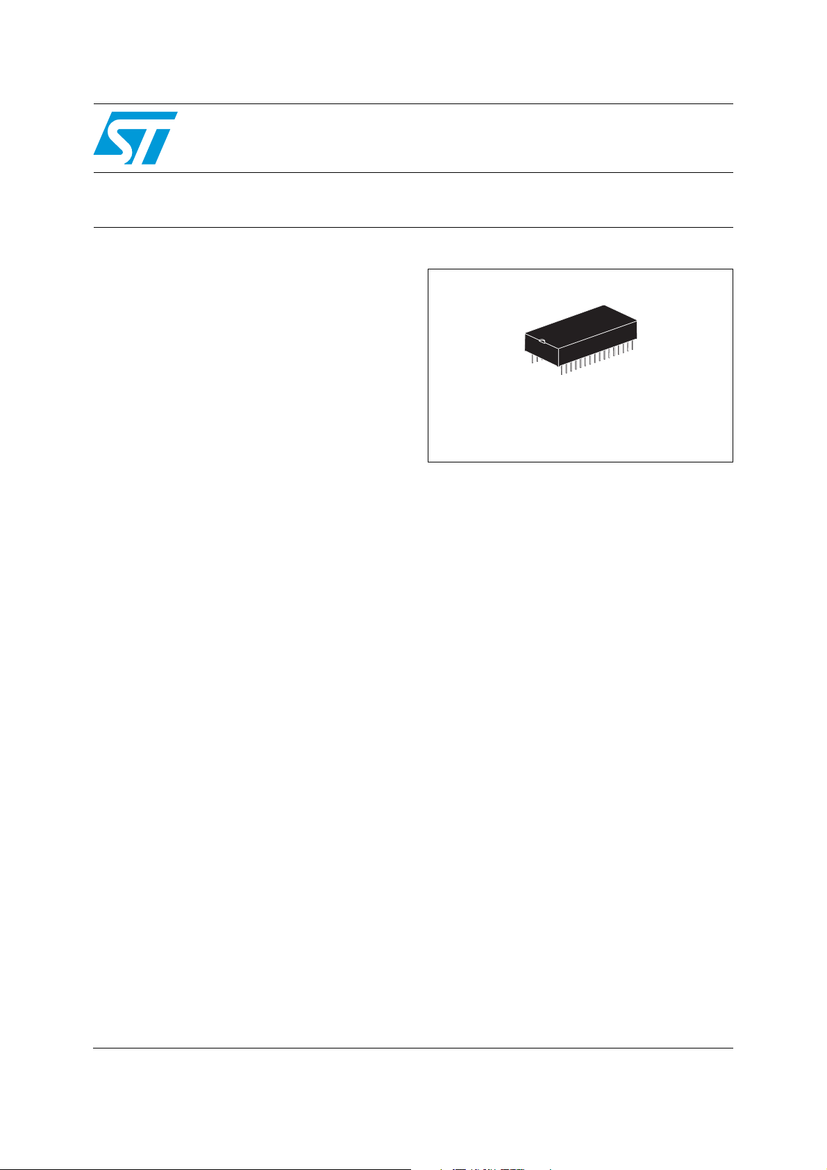
PMDIP32 module
Description
The M48Z512A/Y/V ZEROPOWER® RAM is a
non-volatile, 4,194,304-bit static RAM organized
as 524,288 words by 8 bits. The devices combine
an internal lithium battery, a CMOS SRAM and a
control circuit in a plastic, 32-pin DIP module.
June 2011 Doc ID 5146 Rev 9 1/21
This is information on a product still in production but not recommended for new designs.
www.st.com
1
Page 2

Contents M48Z512A, M48Z512AY, M48Z512AV
Contents
1 Device overview . . . . . . . . . . . . . . . . . . . . . . . . . . . . . . . . . . . . . . . . . . . . 5
2 Operating modes . . . . . . . . . . . . . . . . . . . . . . . . . . . . . . . . . . . . . . . . . . . . 7
2.1 READ mode . . . . . . . . . . . . . . . . . . . . . . . . . . . . . . . . . . . . . . . . . . . . . . . . 7
2.2 WRITE mode . . . . . . . . . . . . . . . . . . . . . . . . . . . . . . . . . . . . . . . . . . . . . . . 9
2.3 Data retention mode . . . . . . . . . . . . . . . . . . . . . . . . . . . . . . . . . . . . . . . . . 11
2.4 V
noise and negative going transients . . . . . . . . . . . . . . . . . . . . . . . . . 12
CC
3 Maximum ratings . . . . . . . . . . . . . . . . . . . . . . . . . . . . . . . . . . . . . . . . . . . 13
4 DC and AC parameters . . . . . . . . . . . . . . . . . . . . . . . . . . . . . . . . . . . . . . 14
5 Package mechanical data . . . . . . . . . . . . . . . . . . . . . . . . . . . . . . . . . . . . 17
6 Part numbering . . . . . . . . . . . . . . . . . . . . . . . . . . . . . . . . . . . . . . . . . . . . 18
7 Environmental information . . . . . . . . . . . . . . . . . . . . . . . . . . . . . . . . . . . 19
8 Revision history . . . . . . . . . . . . . . . . . . . . . . . . . . . . . . . . . . . . . . . . . . . 20
2/21 Doc ID 5146 Rev 9
Page 3

M48Z512A, M48Z512AY, M48Z512AV List of tables
List of tables
Table 1. Signal names . . . . . . . . . . . . . . . . . . . . . . . . . . . . . . . . . . . . . . . . . . . . . . . . . . . . . . . . . . . . 5
Table 2. Operating modes . . . . . . . . . . . . . . . . . . . . . . . . . . . . . . . . . . . . . . . . . . . . . . . . . . . . . . . . . 7
Table 3. READ mode AC characteristics . . . . . . . . . . . . . . . . . . . . . . . . . . . . . . . . . . . . . . . . . . . . . . 9
Table 4. WRITE mode AC characteristics . . . . . . . . . . . . . . . . . . . . . . . . . . . . . . . . . . . . . . . . . . . . 11
Table 5. Absolute maximum ratings . . . . . . . . . . . . . . . . . . . . . . . . . . . . . . . . . . . . . . . . . . . . . . . . . 13
Table 6. Operating and AC measurement conditions . . . . . . . . . . . . . . . . . . . . . . . . . . . . . . . . . . . . 14
Table 7. Capacitance . . . . . . . . . . . . . . . . . . . . . . . . . . . . . . . . . . . . . . . . . . . . . . . . . . . . . . . . . . . . 14
Table 8. DC characteristics. . . . . . . . . . . . . . . . . . . . . . . . . . . . . . . . . . . . . . . . . . . . . . . . . . . . . . . . 15
Table 9. Power down/up AC characteristics . . . . . . . . . . . . . . . . . . . . . . . . . . . . . . . . . . . . . . . . . . . 16
Table 10. Power down/up trip points DC characteristics . . . . . . . . . . . . . . . . . . . . . . . . . . . . . . . . . . 16
Table 11. PMDIP32 – 32-pin plastic DIP module, package mechanical data. . . . . . . . . . . . . . . . . . . 17
Table 12. Ordering information scheme . . . . . . . . . . . . . . . . . . . . . . . . . . . . . . . . . . . . . . . . . . . . . . . 18
Table 13. Revision history . . . . . . . . . . . . . . . . . . . . . . . . . . . . . . . . . . . . . . . . . . . . . . . . . . . . . . . . . 20
Doc ID 5146 Rev 9 3/21
Page 4

List of figures M48Z512A, M48Z512AY, M48Z512AV
List of figures
Figure 1. Logic diagram . . . . . . . . . . . . . . . . . . . . . . . . . . . . . . . . . . . . . . . . . . . . . . . . . . . . . . . . . . . . 5
Figure 2. DIP connections . . . . . . . . . . . . . . . . . . . . . . . . . . . . . . . . . . . . . . . . . . . . . . . . . . . . . . . . . . 6
Figure 3. Block diagram . . . . . . . . . . . . . . . . . . . . . . . . . . . . . . . . . . . . . . . . . . . . . . . . . . . . . . . . . . . . 6
Figure 4. Chip enable or output enable controlled, READ mode AC waveforms. . . . . . . . . . . . . . . . . 8
Figure 5. Address controlled, READ mode AC waveforms . . . . . . . . . . . . . . . . . . . . . . . . . . . . . . . . . 8
Figure 6. WRITE enable controlled, WRITE AC waveforms . . . . . . . . . . . . . . . . . . . . . . . . . . . . . . . 10
Figure 7. Chip enable controlled, WRITE AC waveforms . . . . . . . . . . . . . . . . . . . . . . . . . . . . . . . . . 10
Figure 8. Supply voltage protection . . . . . . . . . . . . . . . . . . . . . . . . . . . . . . . . . . . . . . . . . . . . . . . . . . 12
Figure 9. AC measurement load circuit . . . . . . . . . . . . . . . . . . . . . . . . . . . . . . . . . . . . . . . . . . . . . . . 14
Figure 10. Power down/up mode AC waveforms. . . . . . . . . . . . . . . . . . . . . . . . . . . . . . . . . . . . . . . . . 15
Figure 11. PMDIP32 – 32-pin plastic DIP module, package outline . . . . . . . . . . . . . . . . . . . . . . . . . . 17
Figure 12. Recycling symbols . . . . . . . . . . . . . . . . . . . . . . . . . . . . . . . . . . . . . . . . . . . . . . . . . . . . . . . 19
4/21 Doc ID 5146 Rev 9
Page 5
M48Z512A, M48Z512AY, M48Z512AV Device overview
1 Device overview
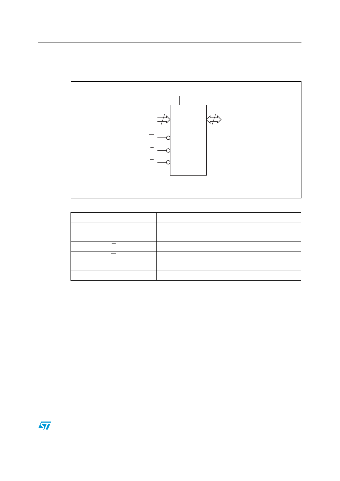
Figure 1. Logic diagram
V
CC
Table 1. Signal names
A0-A18 Address inputs
DQ0-DQ7 Data inputs/outputs
E Chip enable input
G
W
V
CC
V
SS
A0-A18
W
19
M48Z512A
M48Z512AY
E
M48Z512AV
G
V
SS
Output enable input
WRITE enable input
Supply voltage
Ground
8
DQ0-DQ7
AI02043
Doc ID 5146 Rev 9 5/21
Page 6

Device overview M48Z512A, M48Z512AY, M48Z512AV
Figure 2. DIP connections
A18 V
A16
A14
A12
A7
A6
A5
A4
A3
A2
A1
A0
DQ0
DQ2
SS
1
2
3
4
5
6
7
M48Z512A
8
M48Z512AY
9
M48Z512AV
10
11
12
13
14
15
16
32
31
30
29
28
27
26
25
24
23
22
21
20
19
18
17
CC
A15
A17
W
A13
A8
A9
A11
G
A10
E
DQ7
DQ6
DQ5DQ1
DQ4
DQ3V
AI02044
Figure 3. Block diagram
V
CC
POWER
VOLTAGE SENSE
E
AND
SWITCHING
CIRCUITRY
E
INTERNAL
BATTERY
512K x 8
SRAM ARRAY
V
SS
A0-A18
DQ0-DQ7
W
G
AI02045
6/21 Doc ID 5146 Rev 9
Page 7
M48Z512A, M48Z512AY, M48Z512AV Operating modes
2 Operating modes
The M48Z512A/Y/V also has its own power-fail detect circuit. The control circuitry constantly
monitors the single V
tolerance, the circuit WRITE protects the SRAM, providing a high degree of data security in
the midst of unpredictable system operation brought on by low V
switchover voltage (V
until valid power returns.
The ZEROPOWER
PROMs without any requirement for special WRITE timing or limitations on the number of
WRITEs that can be performed.
Table 2. Operating modes
supply for an out of tolerance condition. When VCC is out of
CC
. As VCC falls below the
), the control circuitry connects the battery which maintains data
SO
®
RAM replaces industry standard SRAMs. It provides the nonvolatility of
CC
Mode V
Deselect
WRITE V
READ V
READ V
Deselect V
Deselect ≤ V
1. X = VIH or VIL; VSO = battery backup switchover voltage.
SO
CC
4.75 to 5.5 V
or
4.5 to 5.5 V
or
3.0 to 3.6 V
to V
PFD
SO
(min)
(1)
(1)
Note: See Table 10 on page 16 for details.
2.1 READ mode
The M48Z512A/Y/V is in the READ mode whenever W (WRITE enable) is high and E (chip
enable) is low. The device architecture allows ripple-through access of data from eight of
4,194,304 locations in the static storage array. Thus, the unique address specified by the 19
address inputs defines which one of the 524,288 bytes of data is to be accessed. Valid data
will be available at the data I/O pins within address access time (t
address input signal is stable, providing that the E
access times are also satisfied. If the E
available after the later of chip enable access time (t
(t
). The state of the eight three-state data I/O signals is controlled by E and G. If the
GLQV
outputs are activated before t
until t
. If the address inputs are changed while E and G remain low, output data will
AVQ V
remain valid for output data hold time (t
access.
, the data lines will be driven to an indeterminate state
AVQ V
E G W DQ0-DQ7 Power
V
IH
IL
IL
IL
X X X High Z CMOS standby
X X X High Z Battery backup mode
X X High Z Standby
XVILD
V
V
V
IL
IH
IH
V
IH
IN
D
OUT
High Z Active
) after the last
AVQ V
Active
Active
(chip enable) and G (output enable)
and G access times are not met, valid data will be
) or output enable access Time
ELQV
) but will go indeterminate until the next address
AXQX
Doc ID 5146 Rev 9 7/21
Page 8

Operating modes M48Z512A, M48Z512AY, M48Z512AV
Figure 4. Chip enable or output enable controlled, READ mode AC waveforms
tAVAV
A0-A18
tAVQV tAXQX
tELQV
E
tELQX
G
tGLQX
DQ0-DQ7
VAL ID
tGLQV
DATA OUT
1. WRITE enable (W) = high
Figure 5. Address controlled, READ mode AC waveforms
A0-A18
tAVAV
tAVQV
tEHQZ
tGHQZ
AI01221
tAXQX
DQ0-DQ7
DATA VALID
1. Chip enable (E) and output enable (G) = low, WRITE enable (W) = high
AI01220
8/21 Doc ID 5146 Rev 9
Page 9

M48Z512A, M48Z512AY, M48Z512AV Operating modes
Table 3. READ mode AC characteristics
Symbol Parameter
t
AVAV
t
AVQ V
t
ELQV
t
GLQV
t
ELQX
t
GLQX
t
EHQZ
t
GHQZ
t
AXQX
1. Valid for ambient operating temperature: TA = 0 to 70 °C or –40 to 85 °C; VCC = 4.75 to 5.5 V, 4.5 to 5.5 V,
or 3.0 to 3.6 V (except where noted).
2. CL = 5 pF.
READ cycle time 70 85 ns
Address valid to output valid 70 85 ns
Chip enable low to output valid 70 85 ns
Output enable low to output valid 35 45 ns
(2)
Chip enable low to output transition 5 5 ns
(2)
Output enable low to output transition 5 5 ns
(2)
Chip enable high to output Hi-Z 30 35 ns
(2)
Output enable high to output Hi-Z 20 25 ns
Address transition to output transition 5 5 ns
2.2 WRITE mode
The M48Z512A/Y/V is in the WRITE mode whenever W and E are active. The start of a
WRITE is referenced from the latter occurring falling edge of W
by the earlier rising edge of W
(1)
or E.
M48Z512A/Y
–70
M48Z512A/Y/V
–85
Min Max Min Max
or E. A WRITE is terminated
Unit
The addresses must be held valid throughout the cycle. E
minimum of t
cycle. Data-in must be valid t
t
or t
EHDX
WHDX
EHAX
from E or t
from W prior to the initiation of another READ or WRITE
WHAX
DVE H
or t
prior to the end of WRITE and remain valid for
DVW H
afterward. G should be kept high during WRITE cycles to avoid bus
or W must return high for a
contention; although, if the output bus has been activated by a low on E
will disable the outputs t
after W falls.
WLQZ
and G, a low on W
Doc ID 5146 Rev 9 9/21
Page 10

Operating modes M48Z512A, M48Z512AY, M48Z512AV
Figure 6. WRITE enable controlled, WRITE AC waveforms
tAVAV
A0-A18
tAVEL
E
tAVWL
W
tWLQZ
DQ0-DQ7
VAL ID
tAVWH
tWLWH
tWHDX
DATA INPUT
tDVWH
1. Output enable (G) = high.
Figure 7. Chip enable controlled, WRITE AC waveforms
tAVAV
A0-A18
tAVEL
VAL ID
tAVEH
tELEH
tWHAX
tWHQX
AI01222
tEHAX
E
W
DQ0-DQ7
1. Output enable (G) = high.
tAVWL
tEHDX
DATA INPUT
tDVEH
AI01223
10/21 Doc ID 5146 Rev 9
Page 11

M48Z512A, M48Z512AY, M48Z512AV Operating modes
Table 4. WRITE mode AC characteristics
Symbol Parameter
(1)
M48Z512A/Y
–70
M48Z512A/Y/V
–85
Unit
Min Max Min Max
t
AVAV
t
AVW L
t
AVEL
t
WLWH
t
ELEH
t
WHAX
t
EHAX
t
DVW H
t
DVE H
t
WHDX
t
EHDX
t
WLQZ
t
AVW H
t
AVEH
t
WHQX
1. Valid for ambient operating temperature: TA = 0 to 70 °C or –40 to 85 °C; VCC = 4.75 to 5.5 V, 4.5 to 5.5 V
or 3.0 to 3.6 V (except where noted).
2. CL = 5 pF.
goes low simultaneously with W going low, the outputs remain in the high impedance state.
3. If E
WRITE cycle time 70 85 ns
Address valid to WRITE enable low 0 0 ns
Address valid to chip enable low 0 0 ns
WRITE enable pulse width 55 65 ns
Chip enable low to chip enable high 55 75 ns
WRITE enable high to address transition 5 5 ns
Chip enable high to address transition 15 15 ns
Input valid to WRITE enable high 30 35 ns
Input valid to chip enable high 30 35 ns
WRITE enable high to input transition 0 0 ns
Chip enable high to input transition 10 10 ns
(2)(3)
WRITE enable low to output Hi-Z 25 30 ns
Address valid to WRITE enable high 65 75 ns
Address valid to chip enable high 65 75 ns
(2)(3)
WRITE enable high to output transition 5 5 ns
2.3 Data retention mode
With valid VCC applied, the M48Z512A/Y/V operates as a conventional BYTEWIDE™ static
RAM. Should the supply voltage decay, the RAM will automatically power-fail deselect,
WRITE protecting itself t
and all inputs are treated as “don't care.”
If power fail detection occurs during a valid access, the memory cycle continues to
completion. If the memory cycle fails to terminate within the time t
takes place. When V
energy source which preserves data.
The internal coin cell will maintain data in the M48Z512A/Y/V after the initial application of
V
for an accumulated period of at least 10 years when VCC is less than VSO. As system
CC
power returns and V
is switched to external V
allow for processor stabilization. After t
For more information on battery storage life refer to the application note AN1012.
after VCC falls below V
WP
drops below VSO, the control circuit switches power to the internal
CC
rises above VSO, the battery is disconnected, and the power supply
CC
. WRITE protection continues for tER after VCC reaches V
CC
. All outputs become high impedance,
PFD
, WRITE protection
WP
to
, normal RAM operation can resume.
ER
PFD
Doc ID 5146 Rev 9 11/21
Page 12

Operating modes M48Z512A, M48Z512AY, M48Z512AV
2.4 VCC noise and negative going transients
ICC transients, including those produced by output switching, can produce voltage
fluctuations, resulting in spikes on the V
capacitors are used to store energy which stabilizes the V
bypass capacitors will be released as low going spikes are generated or energy will be
absorbed when overshoots occur. A ceramic bypass capacitor value of 0.1 µF (see Figure 8)
is recommended in order to provide the needed filtering.
In addition to transients that are caused by normal SRAM operation, power cycling can
generate negative voltage spikes on V
one volt. These negative spikes can cause data corruption in the SRAM while in battery
backup mode. To protect from these voltage spikes, ST recommends connecting a schottky
diode from V
CC
to V
(cathode connected to VCC, anode to VSS). (Schottky diode 1N5817
SS
is recommended for through hole and MBRS120T3 is recommended for surface-mount).
Figure 8. Supply voltage protection
V
CC
bus. These transients can be reduced if
CC
that drive it to values below VSS by as much as
CC
V
bus. The energy stored in the
CC
CC
0.1µF DEVICE
V
SS
AI02169
12/21 Doc ID 5146 Rev 9
Page 13

M48Z512A, M48Z512AY, M48Z512AV Maximum ratings
3 Maximum ratings
Stressing the device above the rating listed in the absolute maximum ratings table may
cause permanent damage to the device. These are stress ratings only and operation of the
device at these or any other conditions above those indicated in the operating sections of
this specification is not implied. Exposure to absolute maximum rating conditions for
extended periods may affect device reliability.
Table 5. Absolute maximum ratings
Symbol Parameter Value Unit
Grade 1 0 to 70
T
T
A
STG
Ambient operating temperature
°C
Grade 6 -40 to 85
Storage temperature (VCC off) –40 to 85 °C
Grade 1 0 to 70
T
T
SLD
BIAS
V
IO
Temperature under bias
Grade 6 –40 to 85
(1)
Lead solder temperature for 10 seconds 260 °C
Input or output voltages –0.3 to 7 V
°C
M48Z512A/512AY –0.3 to 7.0 V
V
CC
I
O
P
1. Soldering temperature of the IC leads is to not exceed 260 °C for 10 seconds. Furthermore, the devices
shall not be exposed to IR reflow nor preheat cycles (as performed as part of wave soldering). ST
recommends the devices be hand-soldered or placed in sockets to avoid heat damage to the batteries.
Supply voltage
M48Z512AV –0.3 to 4.6 V
Output current 20 mA
Power dissipation 1 W
D
Caution: Negative undershoots below –0.3 V are not allowed on any pin while in the battery backup
mode.
Doc ID 5146 Rev 9 13/21
Page 14

DC and AC parameters M48Z512A, M48Z512AY, M48Z512AV
4 DC and AC parameters
This section summarizes the operating and measurement conditions, as well as the DC and
AC characteristics of the device. The parameters in the following DC and AC characteristic
tables are derived from tests performed under the measurement conditions listed in the
relevant tables. Designers should check that the operating conditions in their projects match
the measurement conditions when using the quoted parameters.
Table 6. Operating and AC measurement conditions
Parameter M48Z512A/512AY M48Z512AV Unit
Supply voltage (V
) 4.75 to 5.5 V or 4.5 to 5.5 3.0 to 3.6 V
CC
Grade 1 0 to 70 0 to 70
Ambient operating temperature (T
Load capacitance (C
) 100 50 pF
L
)
A
Grade 6 –40 to 85 –40 to 85
Input rise and fall times ≤ 5 ≤ 5ns
Input pulse voltages 0 to 3 0 to 3 V
Input and output timing ref. voltages 1.5 1.5 V
Note: Output Hi-Z is defined as the point where data is no longer driven.
Figure 9. AC measurement load circuit
DEVICE
UNDER
TEST
650Ω
CL = 100 pF
or 30 pF
(1)
1.75V
°C
CL includes JIG capacitance
1. Excluding open drain output pins; 50 pF for M48Z512AV.
Table 7. Capacitance
Symbol Parameter
C
C
IO
1. Effective capacitance measured with power supply at 5 V (M48Z512A/Y) or 3.3 V (M48Z512AV); sampled
only, not 100% tested.
2. Outputs deselected.
3. At 25 °C.
Input capacitance - 10 pF
IN
(3)
Input/output capacitance - 10 pF
(1)(2)
14/21 Doc ID 5146 Rev 9
AI03903
Min Max Unit
Page 15

M48Z512A, M48Z512AY, M48Z512AV DC and AC parameters
Table 8. DC characteristics
Sym Parameter
Test condition
(1)
M48Z512A/Y
–70
M48Z512AV
–85
Min Max Min Max
(2)
I
Input leakage current 0 V ≤ VIN ≤ V
LI
(2)
I
1. Valid for ambient operating temperature: TA = 0 to 70 °C or –40 to 85 °C; VCC = 4.75 to 5.5 V, 4.5 to 5.5 V, or 3.0 to 3.6 V
2. Outputs deselected.
Output leakage current 0 V ≤ V
LO
I
Supply current
CC
Supply current (standby) TTL E = V
I
CC1
I
Supply current (standby) CMOS E ≥ VCC – 0.2 V 5 3 mA
CC2
Input low voltage –0.3 0.8 –0.3 0.6 V
V
IL
Input high voltage 2.2 VCC + 0.3 2.2 VCC + 0.3 V
V
IH
V
Output low voltage IOL = 2.1 mA 0.4 0.4 V
OL
Output high voltage IOH = –1 mA 2.4 2.2 V
V
OH
(except where noted).
OUT
E
= V
outputs open
≤ V
IL
IH
CC
CC
±1 ±1 µA
±1 ±1 µA
115 50 mA
10 4 mA
Unit
Figure 10. Power down/up mode AC waveforms
V
CC
V
(max)
PFD
V
(min)
PFD
VSO
V
SS
INPUTS
(Including E)
OUTPUTS
tWP
VAL ID VAL ID
tF
tFB
tDR
tRB
DON'T CARE
HIGH-Z
tR
tER
RECOGNIZEDRECOGNIZED
AI02385
Doc ID 5146 Rev 9 15/21
Page 16

DC and AC parameters M48Z512A, M48Z512AY, M48Z512AV
Table 9. Power down/up AC characteristics
Symbol Parameter
(2)
t
F
t
FB
(3)
V
(max) to V
PFD
V
(min) to VSS VCC fall time
PFD
PFD
(min) VCC fall time 300 µs
(1)
Min Max Unit
M48Z512A/Y 10
µs
M48Z512AV 150
t
t
RB
V
R
(min) to V
PFD
VSS to V
PFD
(min) V
(max) VCC rise time 10 µs
PFD
rise time 1 µs
CC
M48Z512A/Y 40 150
t
WPT
t
ER
1. Valid for ambient operating temperature: TA = 0 to 70 °C or –40 to 85 °C; VCC = 4.75 to 5.5 V, 4.5 to 5.5 V,
or 3.0 to 3.6 V (except where noted).
2. V
PFD
until 200 µs after V
3. V
PFD
Table 10. Power down/up trip points DC characteristics
Symbol Parameter
WRITE protect time
M48Z512AV 40 250
E recovery time 40 120 ms
(max) to V
(min) to VSS fall time of less than tFB may cause corruption of RAM data.
(min) fall time of less than tF may result in deselection/WRITE protection not occurring
PFD
passes V
CC
PFD
(min).
(1)(2)
Min Typ Max Unit
µs
M48Z512A 4.5 4.6 4.75 V
V
Power-fail deselect voltage
PFD
M48Z512AY 4.2 4.3 4.5 V
M48Z512AV 2.8 2.9 3.0 V
M48Z512A/Y 3.0 V
V
t
DR
1. All voltages referenced to VSS.
2. Valid for ambient operating temperature: T
or 3.0 to 3.6 V (except where noted).
3. At 25 °C; VCC = 0 V.
Battery backup switchover voltage
SO
(3)
Expected data retention time 10 Years
= 0 to 70 °C or –40 to 85 °C; VCC = 4.75 to 5.5 V, 4.5 to 5.5 V,
A
M48Z512AV 2.5 V
16/21 Doc ID 5146 Rev 9
Page 17

M48Z512A, M48Z512AY, M48Z512AV Package mechanical data
5 Package mechanical data
In order to meet environmental requirements, ST offers these devices in different grades of
ECOPACK
specifications, grade definitions and product status are available at: www.st.com.
ECOPACK
®
packages, depending on their level of environmental compliance. ECOPACK®
®
is an ST trademark.
Figure 11. PMDIP32 – 32-pin plastic DIP module, package outline
A1AL
S
N
1
1. Drawing is not to scale.
Table 11. PMDIP32 – 32-pin plastic DIP module, package mechanical data
B
e3
D
e1
E
eA
C
PMDIP
mm inches
Symb
Typ Min Max Typ Min Max
A 9.27 9.52 0.365 0.375
A1 0.38 0.015
B 0.43 0.59 0.017 0.023
C 0.20 0.33 0.008 0.013
D 42.42 43.18 1.670 1.700
E 18.03 18.80 0.710 0.740
e1 2.29 2.79 0.090 0.110
e3 38.10 1.50
eA 14.99 16.00 0.590 0.630
L 3.05 3.81 0.120 0.150
S 1.91 2.79 0.075 0.110
N32 32
Doc ID 5146 Rev 9 17/21
Page 18

Part numbering M48Z512A, M48Z512AY, M48Z512AV
6 Part numbering
Table 12. Ordering information scheme
Example: M48Z 512AY –70 PM 1
Device type
M48Z
Supply voltage and WRITE protect voltage
(1)
= VCC = 4.75 to 5.5 V; V
512A
(1)
512AY
512AV
= VCC = 4.5 to 5.5 V; V
(1)
= VCC = 3.0 to 3.6 V; V
Speed
–70 = 70 ns (for M48Z512A/Y)
= 4.5 to 4.75 V
PFD
= 4.2 to 4.5 V
PFD
= 2.8 to 3.0 V
PFD
–85 = 85 ns (for M48Z512A/Y/V)
Package
PM = PMDIP32
Temperature range
1 = 0 to 70 °C
6 = –40 to 85 °C
1. Device is not recommended for new design. Contact ST sales office for availability.
For other options, or for more information on any aspect of this device, please contact the
ST sales office nearest you.
18/21 Doc ID 5146 Rev 9
Page 19

M48Z512A, M48Z512AY, M48Z512AV Environmental information
7 Environmental information
Figure 12. Recycling symbols
This product contains a non-rechargeable lithium (lithium carbon monofluoride chemistry)
button cell battery fully encapsulated in the final product.
Recycle or dispose of batteries in accordance with the battery manufacturer's instructions
and local/national disposal and recycling regulations.
Doc ID 5146 Rev 9 19/21
Page 20

Revision history M48Z512A, M48Z512AY, M48Z512AV
8 Revision history
Table 13. Revision history
Date Revision Changes
Mar-2000 1 First issue
19-Jul-2000 1.1 M48Z12AV added
15-Jan-2001 1.2 Changed LPSRAM device (Tabl e 2 )
Reformatted; added temperature information (Ta b l e 3 , Ta b le 4 , Ta bl e 7 ,
19-Dec-2001 2
08-Feb-2002 2.1 Remove 85ns speed grade (Ta bl e 3 , Ta bl e 4 , and Ta bl e 8 )
29-May-2002 2.2 Modify reflow time and temperature footnotes (Ta b le 5 )
18-Nov-2002 2.3 Modified SMT text (Figure 1, Figure , and Tabl e 2 )
Ta bl e 8 , Ta b le 9 , and Ta bl e 1 0 ); remove chipset option from Ordering
Information (Ta b le 1 2 ); remove reference to “clock”
17-Sep-2003 2.4
Remove references to M68xxx (obsolete) part (Figure and Tabl e 2 );
update disclaimer
30-Nov-2004 3 Reformatted; remove extended temperature references (Ta bl e 1 2 )
21-Dec-2004 4
Update Marketing Status for qualification, correct drawing (Figure and
Ta bl e 1 2 )
22-Feb-2005 5 IR reflow, SO package updates (Ta bl e 5 )
Document reformatted.
ECOPACK package text added on coverpage.
21-Dec-2006 6
Note 2 concerning Leaded SOIC package removed below Ta bl e 5 .
Updated PMDIP32 package mechanical data in Section 5: Package
mechanical data; updated T
to include Grade 1 (0 to 70°C) and Grade
A
6 (-40 to 85°C).
7-Nov-2008 7
Indicated that M48Z512AV is Not for New Design; removed all
SNAPHAT
®
battery and SOIC package references; updated Section 5:
Package mechanical data.
02-Aug-2010 8
Updated Features, Section 3, Ta bl e 1 2, ECOPACK
added Section 7: Environmental information.
®
text in Section 5;
Devices are not recommended for new design (updated cover page,
24-Jun-2011 9
Ta bl e 1 2 ); updated footnote of Table 5: Absolute maximum ratings;
updated Section 7: Environmental information.
20/21 Doc ID 5146 Rev 9
Page 21

M48Z512A, M48Z512AY, M48Z512AV
Please Read Carefully:
Information in this document is provided solely in connection with ST products. STMicroelectronics NV and its subsidiaries (“ST”) reserve the
right to make changes, corrections, modifications or improvements, to this document, and the products and services described herein at any
time, without notice.
All ST products are sold pursuant to ST’s terms and conditions of sale.
Purchasers are solely responsible for the choice, selection and use of the ST products and services described herein, and ST assumes no
liability whatsoever relating to the choice, selection or use of the ST products and services described herein.
No license, express or implied, by estoppel or otherwise, to any intellectual property rights is granted under this document. If any part of this
document refers to any third party products or services it shall not be deemed a license grant by ST for the use of such third party products
or services, or any intellectual property contained therein or considered as a warranty covering the use in any manner whatsoever of such
third party products or services or any intellectual property contained therein.
UNLESS OTHERWISE SET FORTH IN ST’S TERMS AND CONDITIONS OF SALE ST DISCLAIMS ANY EXPRESS OR IMPLIED
WARRANTY WITH RESPECT TO THE USE AND/OR SALE OF ST PRODUCTS INCLUDING WITHOUT LIMITATION IMPLIED
WARRANTIES OF MERCHANTABILITY, FITNESS FOR A PARTICULAR PURPOSE (AND THEIR EQUIVALENTS UNDER THE LAWS
OF ANY JURISDICTION), OR INFRINGEMENT OF ANY PATENT, COPYRIGHT OR OTHER INTELLECTUAL PROPERTY RIGHT.
UNLESS EXPRESSLY APPROVED IN WRITING BY AN AUTHORIZED ST REPRESENTATIVE, ST PRODUCTS ARE NOT
RECOMMENDED, AUTHORIZED OR WARRANTED FOR USE IN MILITARY, AIR CRAFT, SPACE, LIFE SAVING, OR LIFE SUSTAINING
APPLICATIONS, NOR IN PRODUCTS OR SYSTEMS WHERE FAILURE OR MALFUNCTION MAY RESULT IN PERSONAL INJURY,
DEATH, OR SEVERE PROPERTY OR ENVIRONMENTAL DAMAGE. ST PRODUCTS WHICH ARE NOT SPECIFIED AS "AUTOMOTIVE
GRADE" MAY ONLY BE USED IN AUTOMOTIVE APPLICATIONS AT USER’S OWN RISK.
Resale of ST products with provisions different from the statements and/or technical features set forth in this document shall immediately void
any warranty granted by ST for the ST product or service described herein and shall not create or extend in any manner whatsoever, any
liability of ST.
ST and the ST logo are trademarks or registered trademarks of ST in various countries.
Information in this document supersedes and replaces all information previously supplied.
The ST logo is a registered trademark of STMicroelectronics. All other names are the property of their respective owners.
© 2011 STMicroelectronics - All rights reserved
STMicroelectronics group of companies
Australia - Belgium - Brazil - Canada - China - Czech Republic - Finland - France - Germany - Hong Kong - India - Israel - Italy - Japan -
Malaysia - Malta - Morocco - Philippines - Singapore - Spain - Sweden - Switzerland - United Kingdom - United States of America
www.st.com
Doc ID 5146 Rev 9 21/21
 Loading...