

Page 1
M48Z35AY
M48Z35AV
256 Kbit (32Kb x 8) ZEROP OWER® SRAM
■ INTEGRATED ULTRA LOW POWER SRAM,
POWER-FAIL CONTROL CIRCUIT and
BATTERY
■ READ CYCLE TIME EQUALS WRITE CYCLE
TIME
■ BATTERY LOW FLAG (BOK)
■ AUTOMATIC POWER-FAIL CHIP DESELECT
and WRITE PROTECTION
■ WRITE PROTECT VOLTAGES
= Power-fail Deselect Voltage):
(V
PFD
– M48Z35AY: 4.20V ≤ V
– M48Z35AV: 2.7V ≤ V
■ SELF-CONTAINED BATTERY in the CAPHAT
PFD
PFD
≤ 4.50V
≤ 3.0V
DIP PACKAGE
■ PACKAGING INCLUDES a 28-LEAD SOIC and
SNAPHAT
®
TOP
(to be Ordered Separately)
■ SOIC PACKAGE PROVIDES D IREC T
CONNECTION for a SNAPHAT TOP which
CONTAINS the BATTERY and CRYSTAL
■ PIN and FUNCTION COMPATIBLE with
JEDEC STANDARD 32K x8 SRAMs
SNAPHAT (SH)
Battery
28
28
1
SOH28 (MH)
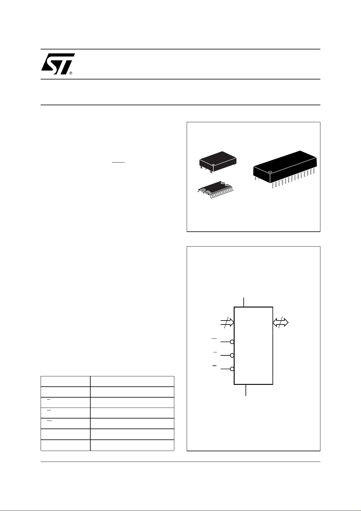
Figure 1. Logic Diagram
V
CC
1
PCDIP28 (PC)
Battery CAPHAT
DESCRIPTION
®
The M48Z35AY/35AV ZEROP OWER
RAM is a
32 Kbit x8 non-volatile static RAM that integrates
power-fail deselect circuitry and battery control
logic on a single die. The monolithi c chip is available in two special packages to provide a highly integrated battery backed-up memory solution.
Table 1. Signal Names
A0-A14 Address Inputs
DQ0-DQ7 Data Inputs / Outputs
E
G
W
V
V
CC
SS
Chip Enable
Output Enable
Write Enable
Supply Voltage
Ground
A0-A14
W
15
M48Z35AY
M48Z35AV
E
G
V
SS
8
DQ0-DQ7
AI02781B
1/16April 2000
Page 2
M48Z35AY, M48Z35AV
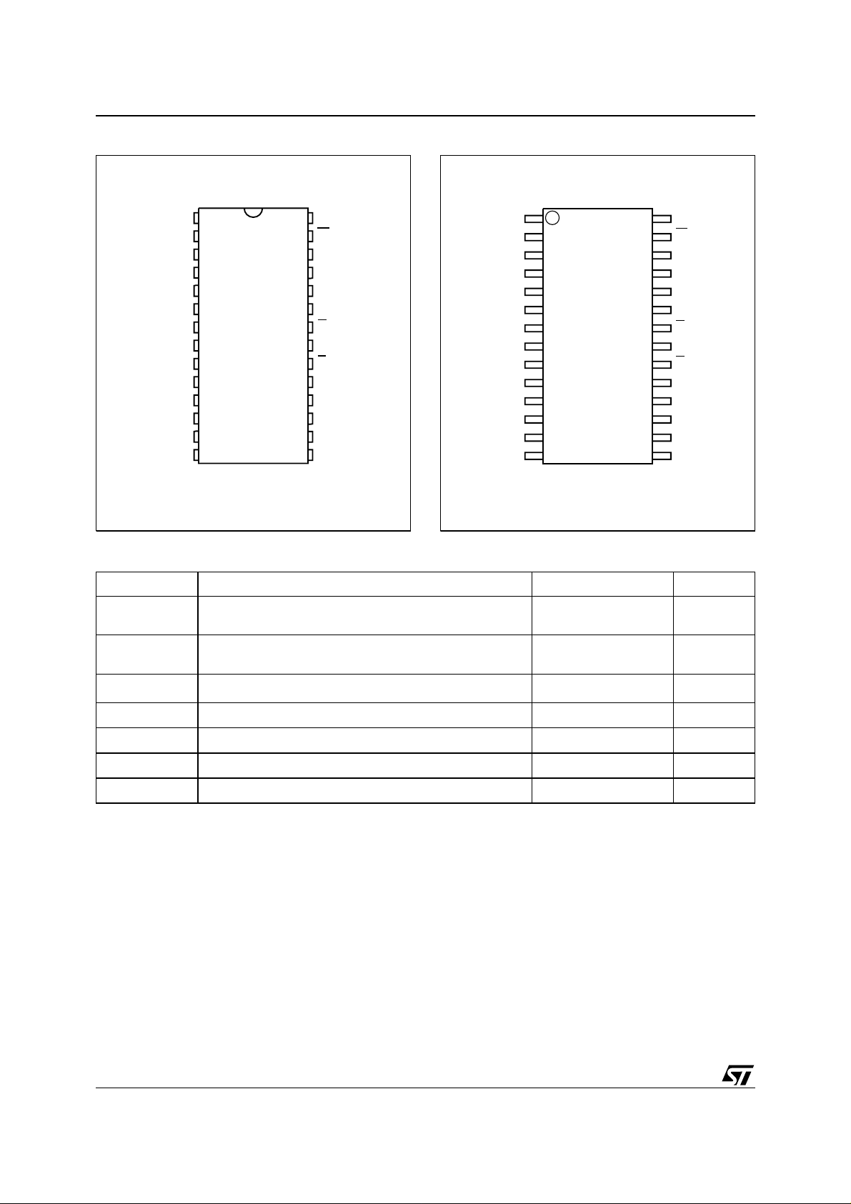
Figure 2A. DIP Pin Connections
A14 V
1
A12
2
3
A7
4
A6
5
A5
6
A4
7
A3
A2
A1
A0
DQ0
M48Z35AY
M48Z35AV
8
9
10
11
12
13
DQ2
14
SS
Table 2. Absolute Maximum Ratings
Symbol Parameter Value Unit
T
A
T
STG
(2)
T
SLD
V
IO
V
CC
I
O
P
D
Note: 1. Stresses greater than those listed under "Absolute Maximum Ratings" may cause permanent damage to the device. This is a stress
rating only and functional operation of the device at these or a ny other conditions above those indicat ed in the operational section
of this spec ification is not im plied. Exposure t o the abso lute max imum rat ing cond itions for extende d period s of tim e may affe ct
reliability.
2. Soldering temperature not to exceed 260°C for 10 seconds (total thermal budget not to exceed 150°C for longer than 30 seconds).
CAUTION: Negative undershoots below –0.3V are not allowed on any pin whil e i n th e Battery Back-up mode.
CAUTION: Do NOT wave solder SOIC to avoid damaging SNAPHAT sockets.
Ambient Operating Temperature Grade 1
Storage Temperature (VCC Off) SNAPHAT
Lead Solder Temperature for 10 seconds 260 °C
Input or Output Voltages –0.3 to 7 V
Supply Voltage –0.3 to 7 V
Output Current 20 mA
Power Dissipation 1 W
28
27
26
25
24
23
22
21
20
19
18
17
16
15
AI02782B
CC
W
A13
A8
A9
A11
G
A10
E
DQ7
DQ6
DQ5DQ1
DQ4
DQ3V
(1)
Grade 6
SOIC
Figure 2B. SOIC Pin Connections
A14 V
A12
A7
A6
A5
A4
A3
A2
A1
A0
DQ0
1
2
3
4
5
6
7
M48Z35AY
M48Z35AV
8
9
10
11
12
DQ2
SS
13
14
0 to 70
–40 to 85
–40 to 85
–55 to 125
28
27
26
25
24
23
22
21
20
19
18
17
16
15
AI02783
CC
W
A13
A8
A9
A11
G
A10
E
DQ7
DQ6
DQ5DQ1
DQ4
DQ3V
°C
°C
2/16
Page 3
M48Z35AY, M48Z35AV
V
PFD
≤ V
CC
or
SO
(1)
(min)
(2)
E G W DQ0-DQ7 Power
V
IH
V
IL
V
IL
V
IL
X X X High Z CMOS Standby
X X X High Z Battery Back-up Mode
Table 3. Operating Modes
Mode
Deselect
Write
Read
Read
Deselect
Deselect
Note: 1. X = VIH or VIL; VSO = Battery Back-up Swit ch ov er Volta ge.
2. See T able 7 for deta ils .
4.5V to 5.5V
3.0V to 3.6V
V
to V
SO
Figure 3. Block Diagram
LITHIUM
CELL
VOLTAGE SENSE
AND
SWITCHING
CIRCUITRY
X X High Z Standby
X
V
IL
V
IH
POWER
V
PFD
V
IL
V
IH
V
IH
32K x 8
SRAM ARRAY
D
IN
D
OUT
High Z Active
Active
Active
A0-A14
DQ0-DQ7
E
W
V
CC
The M48Z35AY/35AV is a non-volatile pin and
function equivalent to any JEDEC standard 32K x8
SRAM. It also easily fits into many ROM, EPROM,
and EEPROM sockets, providing the non-volatility
of PROMs without any requirement for special
write timing or limitations on the number o f writes
that can be performed. The 28 pin 600mil DIP
CAPHAT™ houses the M48Z35AY/35AV silicon
with a long life lithium button cell in a single pa ckage.
G
V
SS
AI01619B
The 28 pin 330mil SOIC provides sockets with
gold plated contacts at both ends for direct connection to a separate SNAPHAT housing cont aining the battery. The unique design allows the
SNAPHAT battery p acka ge t o b e m ount ed o n t op
of the SOIC package after the c ompletion of the
surface mount process. Insertion of the SNAPHAT
housing after reflow prevents potential battery
damage due to the high temperatures required for
device surface-mounting. The SNAPH AT housing
is keyed to prevent reverse insertion.
3/16
Page 4
M48Z35AY, M48Z35AV
Table 4. AC Measurement Conditions
Input Rise and Fall Times ≤ 5ns
Input Pulse Voltages 0 to 3V
Input and Output Timing Ref. Voltages 1.5V
Note that Output Hi-Z is defined as the point where data is no longer
driven.
The SOIC and battery packages are shipped separately in plastic anti-static tubes or in Tape & Reel
form.
For the 28 lead SOIC, the battery package (i.e.
SNAPHAT) part number is "M4Z28-BR00SH1".
The M48Z35AY/35AV also has its own Power-fail
Detect circuit. The control circuitry constantly monitors the single 5V supply for an out of tolerance
condition. When V
is out of tolerance, the circuit
CC
write protects the S RAM, p roviding a high degree
of data security in the midst of unpredictable s ystem operation brought on by low V
CC
. As V
CC
falls
below approximately 3V, the control circuitry connects the battery which maintains data until valid
power returns.
READ MODE
The M48Z35AY/35AV i s in th e Read M ode whenever W
(Write Enable) is high, E (Ch ip Enable) is
low. The device architecture allows ripple-through
access of data from eight of 264,144 locat ions in
the static storage array. Thus, the unique address
specified by the 15 Address Inputs defines which
one of the 32,768 bytes of data is to be accessed.
Valid data will be available at the Data I/O pins
within Address Access time (t
) after the last
AVQV
address input signal is stable, providing that the E
and G access times are also satisfied. If the E and
G
access times are not met, valid data will be
available after the latter of the Chip Enable Access
time (t
(t
GLQV
) or Output Enable Access time
ELQV
).
The state of the eight three-s tate Da ta I/O si gnals
is controlled by E
and G. If the outputs are activat-
Figure 4. AC Testing Load Circuit
DEVICE
UNDER
TEST
CL includes JIG capacitance
ed before t
, the data lines will be driven to an
AVQV
indeterminate state until t
puts are changed while E
645Ω
CL = 100pF or
5pF
. If the Ad dres s In-
AVQV
and G remain active,
1.75V
AI03211
output dat a will rem ain v alid for Outp ut Dat a Hold
time (t
) but will go indeterminate until the next
AXQX
Addr e ss Access.
WRITE MODE
The M48Z35AY/35A V is in the Write Mode whenever W
enced from the latter occurring falling edge of W
E
of W
throughout the cycle. E
a minimum of t
and E are low. The start of a write is refer-
or
. A write is terminated by the earlier rising edge
or E. The addresses must be held valid
or W must return high for
from Chip Enable or t
EHAX
WHAX
from Write Enable prior to the initiation of another
read or write cycle. Data-in must be valid t
prior to the end of write and remain valid for t
DVWH
WHDX
afterward. G should be kept hig h during write cycles to avoid bus contention; although, if the output
bus has been activated by a low on E
will disable the outputs t
on W
WLQZ
and G, a low
after W falls.
4/16
Page 5
M48Z35AY, M48Z35AV
Table 5. Capacitance
(T
= 25 °C)
A
(1, 2)
Symbol Parameter Test Condition Min Max Unit
C
C
IO
Note: 1. Effective capacitan ce measured wi th power su pply at 5V.
2. Sampled only, not 100% tested.
3. Outputs deselect ed.
Input Capacitance
IN
(3)
Input / Output Capacitance
V
V
OUT
IN
= 0V
= 0V
10 pF
10 pF
Table 6. DC Characteristics
(T
= 0 to 70 °C or –40 to 85 °C; VCC = 4.5V to 5.5V or 3.0v to 3.6V)
A
Symbol Parameter Test Condition Min Max Unit
(1)
I
LI
I
LO
I
CC
I
CC1
I
CC2
V
IL
V
IH
V
OL
V
OH
Note: 1. Outputs deselected .
2. Negativ e s p i k e s of –1V allowed for up t o 10 ns once per cycle.
Input Leakage Current
(1)
Output Leakage Current
Supply Current Outputs open 50 mA
Supply Current (Standby) TTL
Supply Current (Standby) CMOS
(2)
Input Low Voltage –0.3 0.8 V
Input High Voltage 2.2
Output Low Voltage
Output High Voltage
0V ≤ V
IN
0V ≤ V
OUT
E
= V
E
= VCC – 0.2V
I
= 2.1mA
OL
I
= –1mA
OH
≤ V
≤ V
IH
CC
CC
±1 µA
±5 µA
3mA
3mA
V
+ 0.3
CC
0.4 V
2.4 V
V
Table 7. Power Down/Up Trip Points DC Characteristics
(1)
(TA = 0 to 70 °C or –40 to 85 °C)
Symbol Parameter Min Typ Max Unit
V
PFD
V
PFD
V
SO
V
SO
t
DR
Note: 1. All voltages referenced to VSS.
2. At 25 ° C.
Power-fail Deselect Voltage (M48Z35AY) 4.2 4.35 4.5 V
Power-fail Deselect Voltage (M48Z35AV) 2.7 2.9 3.0 V
Battery Back-up Switchover Voltage (M48Z35AY) 3.0 V
V
Battery Back-up Switchover Voltage (M48Z35AV)
(2)
Expected Data Retention Time 10 YEARS
PFD
– 100mV
V
5/16
Page 6

M48Z35AY, M48Z35AV
Table 8. Power Down/Up AC Characteristics
(T
= 0 to 70 °C or –40 to 85 °C)
A
Symbol Parameter Min Max Unit
t
PD
t
F
t
FB
t
R
t
RB
t
REC
Note: 1. V
2. V
3. t
E or W at VIH before Power Down
(1)
V
(max) to V
PFD
(2)
V
(3)
PFD
es V
PFD
PFD
(min) = 20ms for industri al tempera ture grade (6) device.
REC
(min) to VSS VCC Fall Time
PFD
V
(min) to V
PFD
VSS to V
V
PFD
(max) to V
(min).
(min) to VSS fall time of less than tFB may cause corruption of RA M data.
(min) VCC Rise Time
PFD
(max) to Inputs Recognized
(min) fall time of less than tF may result in deselection/write protection not occurring until 200µs after VCC pass-
PFD
(min) VCC Fall Time
PFD
(max) VCC Rise Time
PFD
Figure 5. Power Down/Up Mode AC Waveforms
V
CC
V
(max)
PFD
V
(min)
PFD
VSO
tF
tPD
INPUTS
tFB
tDR
tRB
DON'T CARE
0 µs
300 µs
10 µs
10 µs
1µs
40 200 ms
tR
tREC
RECOGNIZEDRECOGNIZED
6/16
OUTPUTS
VALID VALID
(PER CONTROL INPUT)
HIGH-Z
(PER CONTROL INPUT)
AI01168C
Page 7

Table 9. Read Mode AC Characteristics
(T
= 0 to 70 °C or –40 to 85 °C; VCC = 4.5V to 5.5V or 3.0V to 3.6V)
A
M48Z35AY M48Z35AV
M48Z35AY, M48Z35AV
Symbol Parameter
t
AVAV
t
AVQV
t
ELQV
t
GLQV
t
ELQX
t
GLQX
t
EHQZ
t
GHQZ
t
AXQX
Note: 1. CL = 100pF (see Figure 4).
2. C
Read Cycle Time 70 100 ns
(1)
Address Valid to Output Valid 70 100 ns
(1)
Chip Enable Low to Output Valid 70 100 ns
(1)
Output Enable Low to Output Valid 35 50 ns
(2)
Chip Enable Low to Output Transition 5 10 ns
(2)
Output Enable Low to Output Transition 5 5 ns
(2)
Chip Enable High to Output Hi-Z 25 50 ns
(2)
Output Enable High to Output Hi-Z 25 40 ns
(1)
Address Transition to Output Transition 10 10 ns
= 5pF (see Figure 4).
L
Figure 6. Read Mode AC Waveforms.
Unit-70 -100
Min Max Min Max
A0-A14
E
G
DQ0-DQ7
Note: Write Enable (W
) = High.
tAVAV
VALID
tAVQV tAXQX
tELQV
tELQX
tGLQX
tGLQV
tGHQZ
VALID
tEHQZ
AI00925
7/16
Page 8

M48Z35AY, M48Z35AV
Table 10. Write Mode AC Characteristics
(T
= 0 to 70 °C or –40 to 85 °C; VCC = 4.5V to 5.5V or 3.0V to 3.6V)
A
M48Z35AY M48Z35AV
Symbol Parameter
t
AVAV
t
AVWL
t
AVEL
t
WLWH
t
ELEH
t
WHAX
t
EHAX
t
DVWH
t
DVEH
t
WHDX
t
EHDX
(1, 2)
t
WLQZ
t
AVWH
t
AVEH
(1, 2)
t
WHQX
Note: 1. CL = 5pF (see Figure 4).
2. If E
Write Cycle Time 70 100 ns
Address Valid to Write Enable Low 0 0 ns
Address Valid to Chip Enable Low 0 0 ns
Write Enable Pulse Width 50 80 ns
Chip Enable Low to Chip Enable High 55 80 ns
Write Enable High to Address Transition 0 10 ns
Chip Enable High to Address Transition 0 10 ns
Input Valid to Write Enable High 30 50 ns
Input Valid to Chip Enable High 30 50 ns
Write Enable High to Input Transition 5 5 ns
Chip Enable High to Input Transition 5 5 ns
Write Enable Low to Output Hi-Z 25 50 ns
Address Valid to Write Enable High 60 80 ns
Address Valid to Chip Enable High 60 80 ns
Write Enable High to Output Transition 5 10 ns
goes low simultaneously with W going low, the outputs rem ai n in the high impedance stat e.
Unit-70 -100
Min Max Min Max
DATA RETENTION MODE
With valid V
applied, the M48Z35AY/ 35AV op-
CC
erates as a conventional BYTEWIDE™ static
RAM. Should the supply voltage decay, the RAM
will automatically power-fail deselect, write protecting itself when V
(min) window. All outputs become high im-
V
PFD
falls within the V
CC
PFD
(max),
pedance, and all inputs are treated as "don't care."
Note: A power failure during a write cycle may
corrupt data at the currently a ddressed location,
but does not jeopardize the rest of the RAM's content. At voltages below V
(min), the user can be
PFD
assured the memory will be i n a write protected
state, provided the V
fall time is not less than tF.
CC
The M48Z35AY/35AV may respond to transient
noise spikes on V
8/16
that reach into the deselect
CC
window during the time the device is sampling
. Therefore, decoupling of the power supply
V
CC
lines is recommended.
When V
drops below VSO, the control circuit
CC
switches power to the internal battery which preserves data. The internal button cell will maintain
data in the M48Z35AY/35AV for an accumulated
period of at least 10 years (at 25°C) when V
less than V
As system power returns and V
, the battery is disconn ected, and the power
V
SO
supply is switched to external V
tion continues until V
t
(min). Normal RAM operation can resume
REC
after V
t
REC
.
SO
exceeds V
CC
reaches V
CC
PFD
CC
. Write protec-
CC
(max).
rises above
(min) plus
PFD
CC
is
Page 9

Figure 7. Write Enable Controlled, Write AC Waveform
tAVAV
M48Z35AY, M48Z35AV
A0-A14
tAVEL
E
tAVWL
W
tWLQZ
DQ0-DQ7
VALID
tAVWH
tWLWH
Figure 8. Chip Enable Controlled, Write AC Waveforms
tAVAV
tDVWH
tWHAX
tWHQX
tWHDX
DATA INPUT
AI00926
A0-A14
E
W
DQ0-DQ7
tAVEL
tAVWL
VALID
tAVEH
tELEH
DATA INPUT
tDVEH
tEHAX
tEHDX
AI00927
9/16
Page 10

M48Z35AY, M48Z35AV
Figure 9. Checking the BOK Flag Status
POWER-UP
READ DATA
AT ANY ADDRESS
WRITE DATA
COMPLEMENT BACK
TO SAME ADDRESS
READ DATA
AT SAME
ADDRESS AGAIN
IS DATA
COMPLEMENT
OF FIRST
(BATTERY OK)
WRITE ORIGINAL
DATA BACK TO
SAME ADDRESS
CONTINUE
READ?
YES
NO
(BATTERY LOW)
NOTIFY SYSTEM
OF LOW BATTERY
(DATA MAY BE
CORRUPTED)
AI00607
Also, as VCC rises, the battery voltage is checked.
If the voltage is less than approxima tely 2.5V, an
internal Battery Not OK (BOK
BOK
flag can be checked after power up. If the
BOK
flag is set, the first write at tempted will be
) flag will be set. The
blocked. The flag is automatically cleared after the
first write, and normal RAM operation resumes.
Figure 9 illustrates how a BOK
check routine could
be structured.
For more information on Battery Storage Life refer
to the Application Note AN1012.
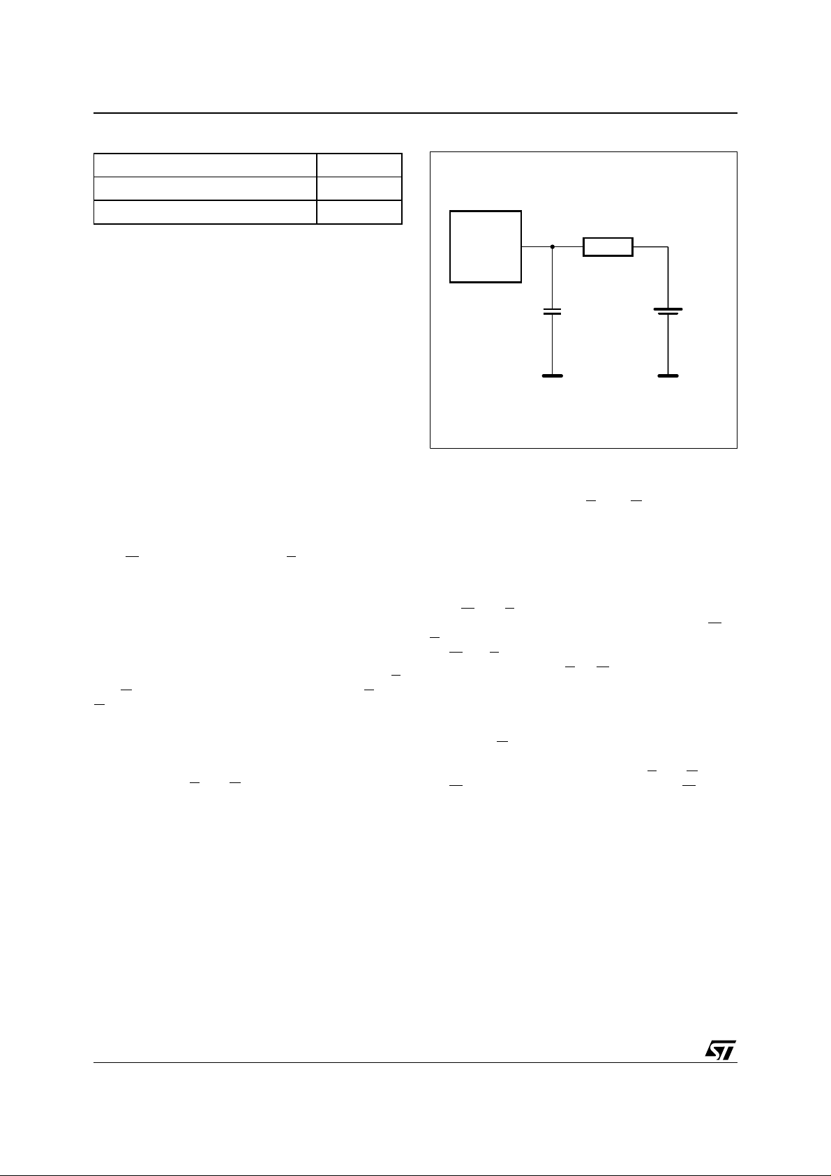
Figure 10. Supply Voltage Protection
V
CC
V
CC
0.1µF DEVICE
V
SS
AI02169
POWER SUPPLY DECOUPLING and
UNDERSHOOT PROTECTION
I
transients, including those produced by output
CC
switching, can produce voltage fluctuations, resulting in spikes on the V
bus. These transients
CC
can be reduced if capacitors are used to store energy, which stabilizes the V
bus. The energy
CC
stored in the bypass capacitors will be released as
low going spikes are generated or energy will be
absorbed when overshoots occur. A ceramic by-
pass capacitor value of 0.1µF (as shown in Figure
10) is recommended in order to provide the needed filtering.
In addition to transients that are caused by normal
SRAM operation, power cycling can generate negative voltage spikes on VCC that drive it to values
below V
by as much as one Volt. These nega-
SS
tive spikes can cause data corruption in the SRAM
while in battery backup mode. To protect from
these voltage spikes, it is recommended to connect a schottky diode from V
connected to V
, anode to VSS). Schottky diode
CC
to VSS (cathode
CC
1N5817 is recommended for through hole and
MBRS120T3 is recommended for surface mount.
10/16
Page 11

M48Z35AY, M48Z35AV
Table 11. Ordering Information Scheme
Example: M48Z35AY -70 MH 1 TR
Supply Voltage and Write Protect Voltage
35AY = V
35AV = V
Speed
-70 = 70ns (M48Z35AY)
-100 = 100ns (M48Z35AV)
Package
PC = PCDIP28
(1)
MH
Temperature Range
1 = 0 to 70 °C
(2)
6
= –40 to 85 °C
Shipping Method for SOIC
blank = Tubes
TR = Tape & Reel
= 4.5V to 5.5V; V
CC
= 3.0V to 3.6V; V
CC
= SOH28
= 4.2V to 4.5V
PFD
= 2.7V to 3.0V
PFD
Note: 1. The SOIC pa ck age (SOH28) requires the battery packa ge (SNAPHAT) which is orde red separat el y under the part n um ber
"M4Zxx-BR00SH1" in plastic tube or "M4Zxx-BR00SH1TR" in Tape & Reel form.
2. Industrial temperature grade available in SOIC package (SOH28) only.
Caution: Do not place t he SNAP HAT battery package " M4Z28-BR00SH1" i n con ductive foam s ince wi ll drain the lithium button-c ell bat tery.
For a list of available options (Speed, Pac kage, etc...) or for furthe r information on any aspect of this device, please contact the STMicroelectronics Sales Office nearest to you.
Table 12. Revision History
Date Revision Details
September 1999 First Issue
04/20/00 SH and SH28 packages for 2-pin and 2-socket removed
11/16
Page 12

M48Z35AY, M48Z35AV
Table 13. PCDIP28 - 28 pin Plastic DIP, battery CAPHAT, Package Mechanical Data
Symb
Typ Min Max Typ Min Max
A 8.89 9.65 0.350 0.380
A1 0.38 0.7 6 0.015 0.030
A2 8.38 8.8 9 0.330 0.350
B 0.38 0.53 0.015 0.021
B1 1.14 1.7 8 0.045 0.070
C 0.20 0.3 1 0.008 0.012
D 39.37 39.88 1.550 1.570
E 17.83 18.34 0.702 0.722
e1 2.29 2.79 0.090 0.110
e3 29.72 36.32 1. 170 1.430
eA 15.24 16.00 0.600 0.630
L 3.05 3.8 1 0.120 0.150
N 28 28
mm inches
Figure 11. PCDIP28 - 28 pin Plastic DIP, battery CAPHAT, Package Outline
A2
A1AL
B1 B e1
eA
e3
D
N
E
1
Drawing is not to scale.
C
PCDIP
12/16
Page 13

M48Z35AY, M48Z35AV
Table 14. SOH28 - 28 lead Plastic Small Outline, battery SNAPHAT, Package Mechanical Data
Symb
Typ Min Ma x Typ Min Max
A 3.05 0.120
A1 0.05 0.3 6 0.002 0.014
A2 2.34 2.6 9 0.092 0.106
B 0.36 0.51 0.014 0.020
C 0.15 0.3 2 0.006 0.012
D 17.71 18.49 0.697 0.728
E 8.23 8.89 0.324 0.350
e 1.27 – – 0.050 – –
eB 3.20 3.6 1 0.126 0.142
H 11.51 12.70 0.453 0.500
L 0.41 1.2 7 0.016 0.050
α 0° 8° 0° 8°
N 28 28
mm inches
CP 0.10 0.004
Figure 12. SOH28 - 28 lead Plastic Small Outline, battery SNAPHAT, Package Outline
A2
A
C
Be
eB
CP
D
N
E
H
LA1 α
1
SOH-A
Drawing is not to scale.
13/16
Page 14

M48Z35AY, M48Z35AV
Table 15. SH - SNAPHAT Housing for 48 mAh Battery, Package Mechanical Data
Symb
Typ Min Max Typ Min Max
A 9.78 0.385
A1 6.73 7.24 0.265 0.285
A2 6.48 6.99 0.255 0.275
A3 0.38 0.015
B 0.46 0.56 0.018 0.022
D 21.21 21.84 0.835 0.860
E 14.22 14.99 0.560 0.590
eA 15.55 15.95 0.612 0.628
eB 3.20 3.61 0.126 0.142
L 2.03 2.29 0.080 0.090
mm inches
Figure 13. SH - SNAPHAT Housing for 48 mAh Battery, Package Outline
A1
A
eA
B
D
E
Drawing is not to scale.
A2
A3
L
eB
SHZP-A
14/16
Page 15

M48Z35AY, M48Z35AV
Table 16. SH - SNAPHAT Housing for 120 mAh Battery, Package Mechanical Data
Symb
Typ Min Max Typ Min Max
A 10.54 0.415
A1 8.00 8.51 0.315 0.335
A2 7.24 8.00 0.285 0.315
A3 0.38 0.015
B 0.46 0.56 0.018 0.022
D 21.21 21.84 0.835 0.860
E 17.27 18.03 0.680 0.710
eA 15.55 15.95 0.612 0.628
eB 3.20 3.61 0.126 0.142
L 2.03 2.29 0.080 0.090
mm inches
Figure 14. SH - SNAPHAT Housing for 120 mAh Battery, Package Outline
A1
A
eA
B
D
E
Drawing is not to scale.
A2
A3
L
eB
SHZP-A
15/16
Page 16

M48Z35AY, M48Z35AV
Information furnishe d is bel i eved to be accurate and reliable. However, STM icroelectro ni cs assumes no responsibility for t he consequ ences
of use of such information nor for any infringement of patents or other rights of third parties which may result from its use. No license is granted
by implic ation or oth erwise under any patent or patent rights of S T M i croelectr onics. Spec i fications mentioned in this publ ic at ion ar e subject
to change without notice. This publication supersedes and replaces all information previously supplied. STMicroelectronics products are not
authorized for use as critical components in life support devices or systems wi thout express written ap proval of STMicroelectro nics.
The ST log o i s registered trademark of STM i croelect ronics
2000 STMicroel e ctronics - All Ri ghts Reserved
All other names are the property of their respec tive owners.
Australi a - Brazil - Chin a - Finland - France - Germ any - Hong Kong - India - Italy - Japan - Malaysi a - M al ta - Morocc o -
Singapor e - Spain - Swede n - Switzerla nd - United Kingdom - U.S.A .
STMicroelect ro n ics GRO UP OF COMPANI ES
http://www.st.com
16/16
 Loading...