

Page 1
Single Chip 8 Mbit (1Mb x8 or 512Kb x16) Flash and
256 Kbit Parallel EEPROM Memory
2.7V to 3.6V SUPPLY VOLTAGE for
PROGRAM, ERASE and READ OPARATIONS
FLASH ARR A Y
– Boot block (Top or Bottom location)
– Parameter and Main blocks
– Selectable x8/x16 Data Bus (
EEPROM ARRAY
– x8 Data Bus only.
120ns ACCESS TIME
(Flash and EEPROM array)
WRITE, PROGRAM and ERASE STATUS BITS
CONCURRENT MODE (Read Flash while
writing to EEPROM)
100,000 ERASE/WRITE CYCLES
10 YEARS DA TA RETE NT ION
LOW POWER CONSUMPTION
– Stand-by mode: 100µA
– Automatic Stand-by mode
64 bytes ONE TIME PROGRAMMABLE
MEMORY (x8 Data Bus only)
ST A NDA RD EPRO M /OTP MEMORY
P ACKAGE
EXTENDED TEMPERATURE RANGES
BYTE pin).
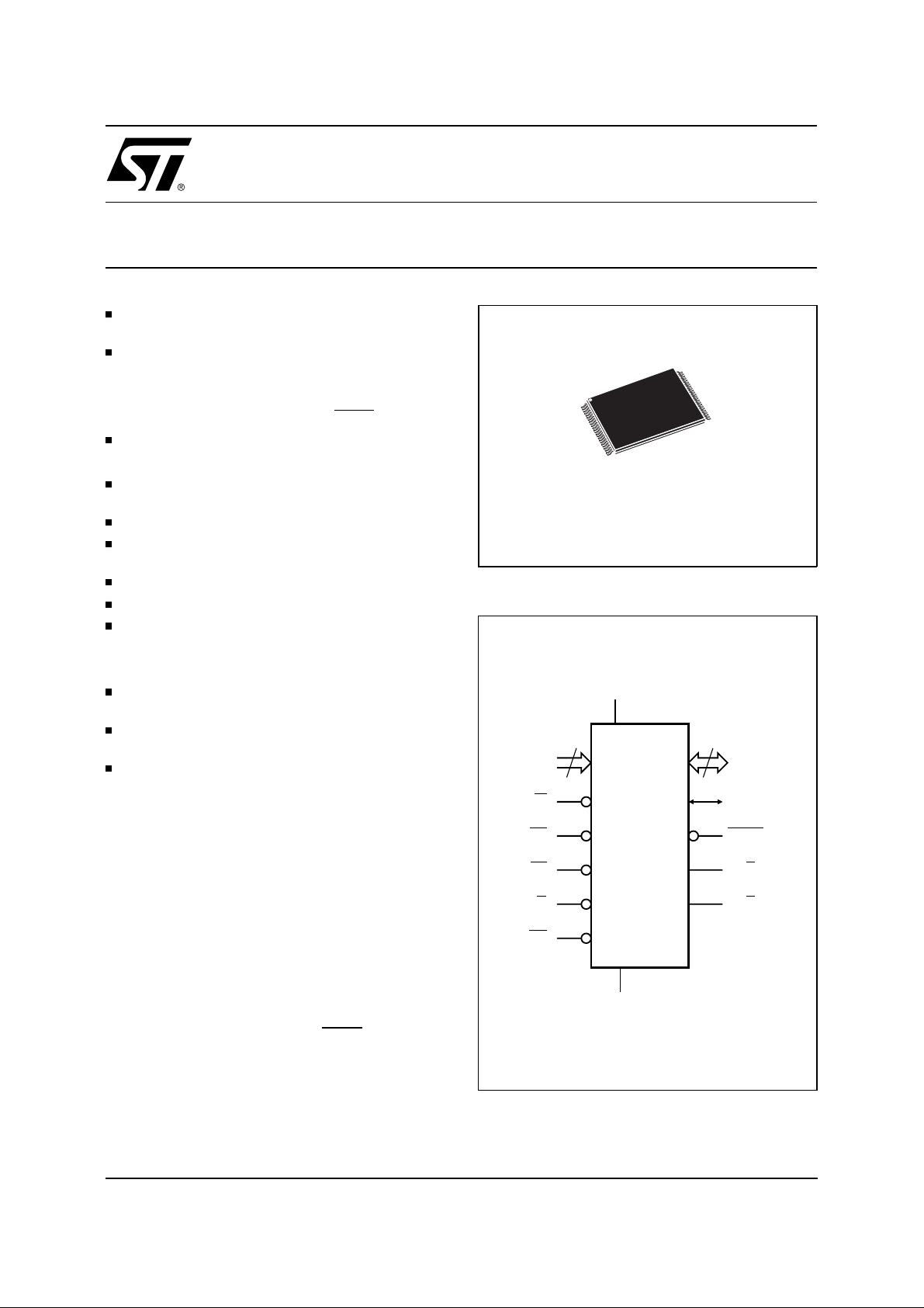
TSOP48 (NE)
12 x 20 mm
Figure 1. Logic Diagram
V
CC
19
A0-A18
M39832
PRELIMINARY DATA
15
DQ0-DQ14
DESCRIPTION
The M39832 is a memory device combining Flash
and EEPROM into a single chip and using single
supply voltage. The memory is mapped in two
arrays: 8 Mbit of Flash memory and 256 Kbit of
W
EE
EF
M39832
G
DQ15A–1
BYTE
ERB
FRB
EEPROM memory. Each space is independant for
writing, in concurrent mode the Flash Memory can
RP
be read while the EEPROM is being written.
An additional 64 bytes of EPROM are One Time
Programmable.
The M39832 EEPROM memory array is organized
in byte only (regardless on the
BYTE pin). It may
V
SS
AI00844
be written by byte or by page of 64 bytes and the
integrity of the data can be secured with the help
of the Software Data Protection (SDP).
February 1999 1/36
This is preliminary information on a new product now in development or undergoing evaluation. Details are subject to change with out not i ce.
Page 2
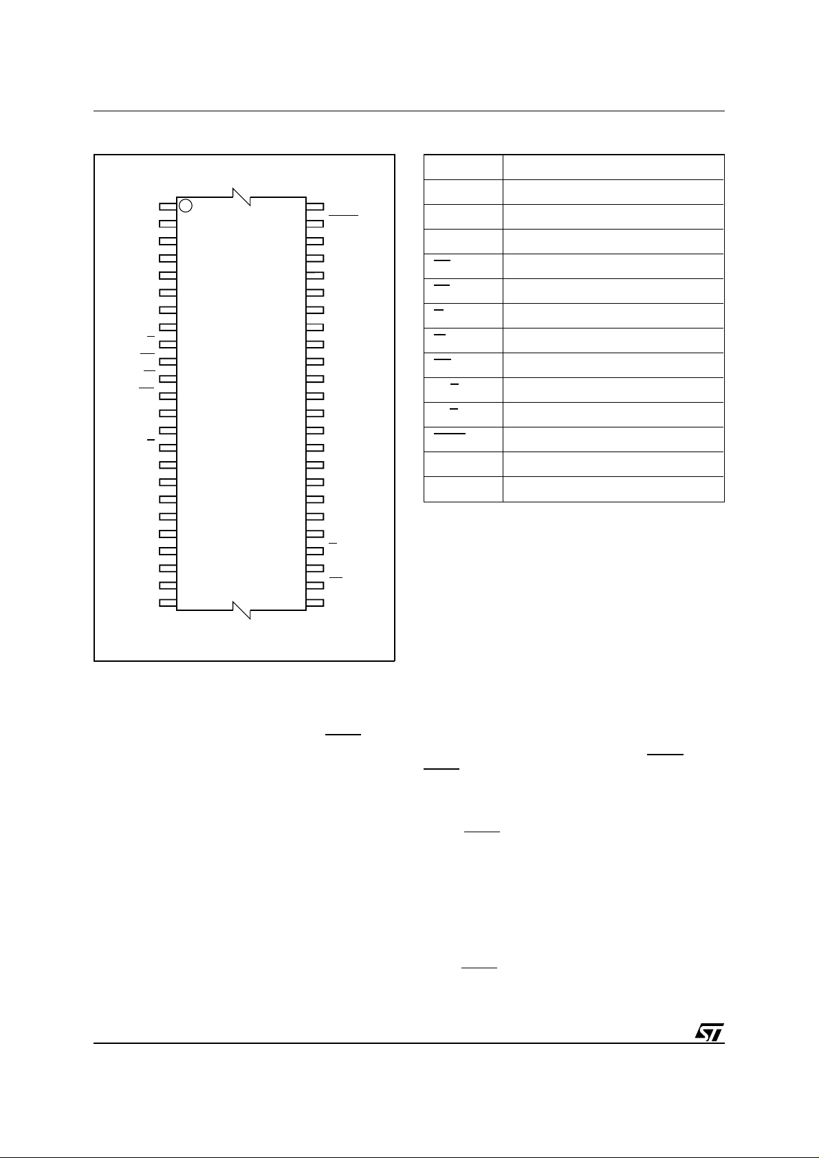
M39832
Figure 2. TSOP Pin Connections
A15
A14
A13
A12
A11
A10
ERB DQ5
EE
RP
NC
NC
FRB
A18
A17
Warning:
DESCRIPTION
1
A9
A8 DQ13
W
12
M39832
13
A7
A6
A5 DQ0
A4 G
A3
A2
24 25
A1
NC = Not Connected.
(cont’d)
48
37
36
AI00845
A16
BYTE
V
SS
DQ15A–1
DQ7
DQ14
DQ6
DQ12
DQ4
V
CC
DQ11
DQ3
DQ10
DQ2
DQ9
DQ1
DQ8
V
SS
EF
A0
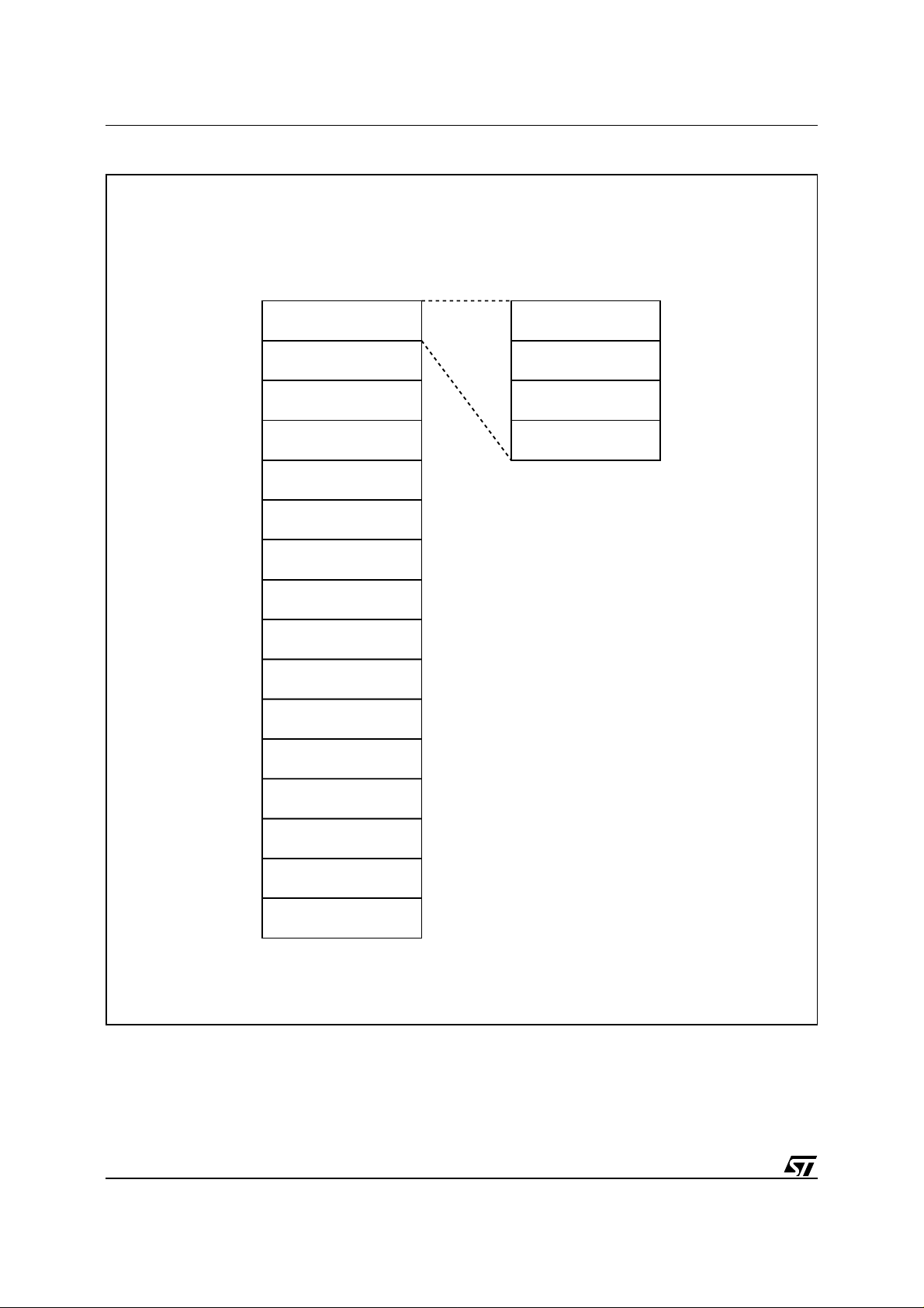
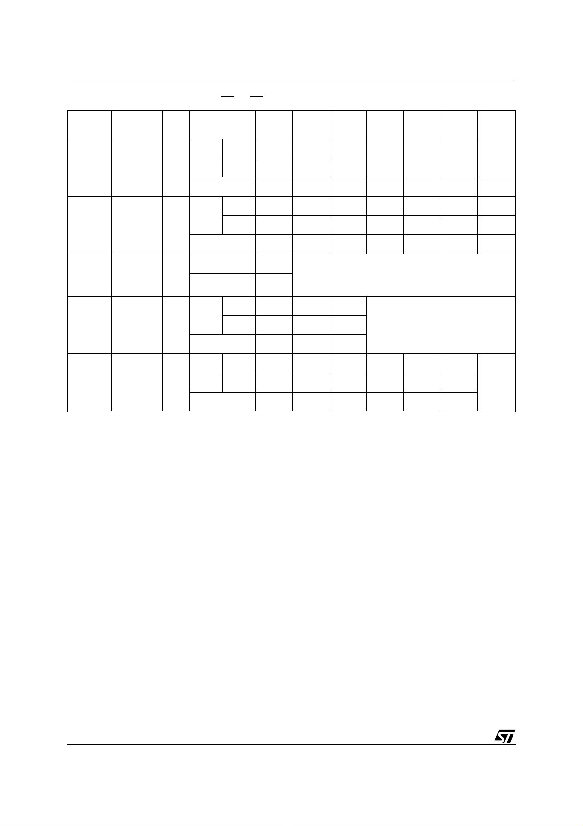
The M39832 Flash Memory array can be configured as 1Mb x8 or 512Kb x16 with the
BYTE input
pin. The M39832-T and M39832-B feature asymetrically blocked architecture providing system memory integration. Both M39832-B and M39832-T
devices have a Flash array of 19 blocks, one Boot
Block of 16 KBytes or 8 KWords, two Parameter
Blocks of 8 KBytes or 4 KWords, one Main Block
of 32 KBytes or 16 KW ords and fifteen Main Blocks
of 64 KBytes or 32 KWords. The M39832-T has the
Boot Block at the top of the memory address space
and the M39832-B locates the Boot Block starting
at the bottom. The memory maps are showed in
Figures 3A and 3B. Each block can be erased
separately ,any combination of blocks can be specified for multi-block erase or the entire chip may be
erased. The Erase operations are managed automatically. The block erase operation can be sus-
Tabl e 1. Signal Names
A0-A18 Address Inputs
DQ0-DQ7 Data Input/Outputs, Commands Input
DQ8-DQ14 Data Input/Outputs
DQ15A–1 Data Input/Outputs or Address Input
EE EEPROM Array Enable
EF Flash Array Enable
G Output Enable
W Write Enable
RP Reset/Block Temporary Unprotect
ER
B EEPROM Ready/Busy Output
B Flash Ready/Busy Output
FR
BYTE Flash Array Byte/Word Organization
V
CC
V
SS
Supply Voltage
Ground
pended in order to read from or program to any
block not being ersased, and then resumed. Block
protection provides additional data security. Each
block can be separately protected or unprotected
against Program or Erase on programming equipment. All previously protected blocks can be temporarily unprotected in the applic ation. The Flash
memory array is functionally compatible with the
M29W800 Single Voltage Flash Memory device.
During a Program or Erase cycle in the F lash array
or during a Write in the EE PR OM ar ray, status bits
available on certain DQn pins provide information
on the M39832 internal logic.
PIN DESCRIPTION
. The
Byte/Word Organization Select (
BYTE)
BYTE input selects the output configuration for the
Flash array: Byte-wide (x8) mode or Word-wide
(x16) mode. The EEPROM array and the 64 Bytes
OTP Row are always accessed Byte-wide (x8).
BYTE is High, the Word-wide mode is se-
When
lected for the Flash array ( x16) and the data are
read and programmed on DQ0-DQ15. The Flash
array is accessed with A0-A18 Adrress lines. In this
mode, data in the EEPROM array (x8) are read and
programmed on DQ0-DQ7 and the array is accessed with A0-A14. The 64 bytes OTP are read
and programmed on DQ0-DQ7 and are accessed
with A0-A5 and A6 = 0.
BYTE is Low , the Byte-wide mode is selected
When
for the Flash array (x8) and the data are read and
2/36
Page 3

M39832
Table 2. Absolute Maximum Ratings
Symbol Parameter Value Unit
T
A
T
BIAS
T
STG
(2)
V
IO
V
CC
, VG, V
V
A9
Notes:
EF
1. Except for the rating "Operating Temperature Range", stresses above those listed in the Table "Absolute Maximum Ratings"
may cause permanent damage to the device. These are stress ratings only and operation of the device at these or any other
conditions above those indicated in the Operating sections of this specification is not implied. Exposure to Absolute Maximum
Rating conditions for extended periods may affect device reliability. Refer also to t he STMicroelectroni cs SURE Pro gr am and other
relevant quality documents.
2. Minimum Voltage may undershoot to –2V during transition and for less than 20ns.
Ambient Operating Temperature –40 to 85
Temperature Under Bias –50 to 125
Storage Temperature –65 to 150
Input or Output Voltages –0.6 to 5 V
Supply Voltage –0.6 to 5 V
(2)
A9, G, EF Voltage –0.6 to 13.5 V
programmed on DQ0-DQ7. In this mode, DQ8DQ14 are at high impedance and DQ15A–1 is the
LSB address bit, making the Flash array to be
accessed with A–1-A18 Adress lines. In this mode,
data in the EEPROM array (x8) are read and
programmed on DQ0-DQ7 and the array is accessed with A–1-A13. The 64 bytes OTP are read
and programmed on DQ0-DQ7 and are accessed
with A-1 - A4 and A6 = 0.
Address Inputs (A0-A18).
The address inputs for
the memory array are latched during a write operation on the falling edge at Chip Enable (
or Write Enable
W. In Word-wide organisation the
address lines are A0-A18, in Byte-wide organisation DQ15A–1 acts as an additional LSB address
line. When A9 is raised to V
ID
Electronic Signature Manufacturer or Device Code,
Block Protection Status or a Write Block Protection
or Block Unprotection is enabled depending on the
combination of levels on A0, A1, A6, A12 and A15.
Data Input/Output (DQ0-DQ7).
puts/Outputs are used in the Byte-wide and Wordwide organisations. The input is data to be
programmed in the memory array or a comma nd
to be written. Both are latched on the rising edge
of Chip Enable (
EE or EF) or Write Enable W. The
output is data from the Memory Array, the Electronic Signature Manufacturer or Device codes, the
Block Protection Status or t he S tatus r egister Data
Polling bit DQ7, the T oggle Bits DQ6 and DQ2, the
Error bit DQ5 or the Erase Timer bit DQ3. Outputs
are valid when Chip Enable (
Enable
G are active. The output is high impedance
EE or EF) and Output
when the chip is deselected or the outputs are
disabled and when
RP is at a Low level.
Data Input/Outputs ( DQ8-DQ14 and DQ15A–1).
(1)
EE or EF)
, either a Read
These In-
DQ14 and DQ15A–1 act as the MSB of the Data
Input or Output, functioning as described for DQ0DQ7 above, and DQ8 - DQ15 are ’don’t care’ for
command inputs or status outputs. When
Low , DQ8-DQ14 are high impedance, DQ15A–1 is
the Address A–1 input.
Memory Array En able (
Array Enable (
EE or EF) activates the memory
EE and EF).
control logic, input buffers, decoders and sense
amplifiers. When the
EE input is driven high, the
EEPROM memory array is not selected; when the
EF input is driven high, the Flash memory array is
not selected. Attempts to access both EEPROM
and Flash arrays (
EE low and EF low) are forbidden. Switching between the two memory array
enables (
EE and EF) must not be made on the
same clock cycle, a delay of greater than t
be inserted.
The M39832 is in standby when both
are High (when no internal Erase or programming
is running). The power consumption is reduced to
the standby level and the outputs are in the high
impedance state, independent of the Output En-
G or Write Enable W inputs.
able
After 150ns of inactivity and when the addresses
are driven at CMOS levels, the chip automatically
enters a pseudo standby mode where consumption
is reduced to the CMOS standby value, while the
outputs continue to drive the bus.
The Output Enable gates the
Output Enable (
G).
outputs through the data buffers during a read
operation. The data outputs are in the high impedance state when the Output Enable
During Block Protect and Block Unprotect operations, the
G input must be forced to VID level (12V
+ 0.5V) (for Flash memory array only).
These Inputs/Outputs are additionally used in the
Word-wide organisation. W hen
BYTE is High DQ8-
C
°
C
°
C
°
BYTE is
The Memory
must
EHFL
EF and EE
G is High.
3/36
Page 4
M39832
Figure 3A. Top Boot Block Memory Map and Block Address Table
TOP BOOT BLOCK
7FFFFh
78000h
77FFFh
70000h
6FFFFh
68000h
67FFFh
60000h
5FFFFh
58000h
57FFFh
50000h
4FFFFh
48000h
47FFFh
40000h
3FFFFh
38000h
37FFFh
30000h
2FFFFh
28000h
27FFFh
20000h
1FFFFh
18000h
17FFFh
10000h
0FFFFh
08000h
07FFFh
00000h
Byte-WideWord-Wide
FFFFFh
F0000h
EFFFFh
E0000h
DFFFFh
D0000h
CFFFFh
C0000h
BFFFFh
B0000h
AFFFFh
A0000h
9FFFFh
90000h
8FFFFh
80000h
7FFFFh
70000h
6FFFFh
60000h
5FFFFh
50000h
4FFFFh
40000h
3FFFFh
30000h
2FFFFh
20000h
1FFFFh
10000h
0FFFFh
00000h
64K MAIN BLOCK
64K MAIN BLOCK
64K MAIN BLOCK
64K MAIN BLOCK
64K MAIN BLOCK
64K MAIN BLOCK
64K MAIN BLOCK
64K MAIN BLOCK
64K MAIN BLOCK
64K MAIN BLOCK
64K MAIN BLOCK
64K MAIN BLOCK
64K MAIN BLOCK
64K MAIN BLOCK
64K MAIN BLOCK
16K BOOT BLOCK
8K PARAMETER BLOCK
8K PARAMETER BLOCK
32K MAIN BLOCK
AI01725B
Byte-Wide Word-Wide
FFFFFh
FC000h
FBFFFh
FA000h
F9FFFh
F8000h
F7FFFh
F0000h
7FFFFh
7E000h
7DFFFh
7D000h
7CFFFh
7C000h
7BFFFh
78000h
4/36
Page 5
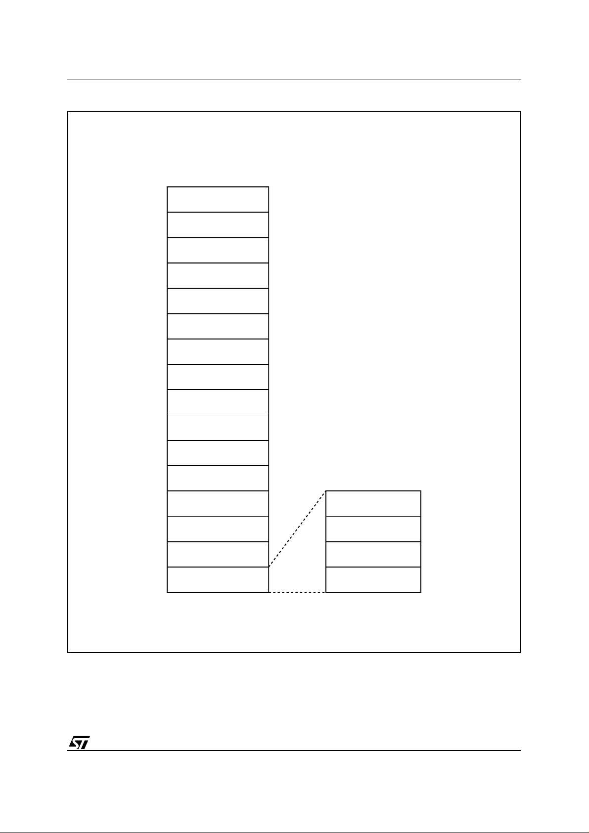
Figure 3B. Bottom Boot Block Memory Map and Block Address T able
BOTTOM BOOT BLOCK
Byte-WideWord-Wide
FFFFFh
78000h
77FFFh
70000h
6FFFFh
68000h
67FFFh
60000h
5FFFFh
58000h
57FFFh
50000h
4FFFFh
48000h
47FFFh
40000h
3FFFFh
38000h
37FFFh
30000h
2FFFFh
28000h
27FFFh
20000h
1FFFFh
18000h
17FFFh
10000h
0FFFFh
08000h
07FFFh
00000h
FFFFFh7FFFFh
F0000h
EFFFFh
E0000h
DFFFFh
D0000h
CFFFFh
C0000h
BFFFFh
B0000h
AFFFFh
A0000h
9FFFFh
90000h
8FFFFh
80000h
7FFFFh
70000h
6FFFFh
60000h
5FFFFh
50000h
4FFFFh
40000h
3FFFFh
30000h
2FFFFh
20000h
1FFFFh
10000h
0FFFFh
00000h
64K MAIN BLOCK
64K MAIN BLOCK
64K MAIN BLOCK
64K MAIN BLOCK
64K MAIN BLOCK
64K MAIN BLOCK
64K MAIN BLOCK
64K MAIN BLOCK
64K MAIN BLOCK
64K MAIN BLOCK
64K MAIN BLOCK
64K MAIN BLOCK
64K MAIN BLOCK
64K MAIN BLOCK
64K MAIN BLOCK
32K MAIN BLOCK
8K PARAMETER BLOCK
8K PARAMETER BLOCK
16K BOOT BLOCK
M39832
Byte-Wide Word-Wide
0FFFFh
08000h
07FFFh
06000h
05FFFh
04000h
03FFFh
00000h
07FFFh
04000h
03FFFh
03000h
02FFFh
02000h
01FFFh
00000h
AI01731B
5/36
Page 6
M39832
T ab le 3A. M39832-T Block Address T ab le
Address Range (x8) Address Range (x16) A18 A17 A16 A15 A14 A13 A12
00000h-0FFFFh 00000h-07FFFh 0000XXX
10000h-1FFFFh 08000h-0FFFFh 0001XXX
20000h-2FFFFh 10000h-17FFFh 0010XXX
30000h-3FFFFh 18000h-1FFFFh 0011XXX
40000h-4FFFFh 20000h-27FFFh 0100XXX
50000h-5FFFFh 28000h-2FFFFh 0101XXX
60000h-6FFFFh 30000h-37FFFh 0110XXX
70000h-7FFFFh 38000h-3FFFFh 0111XXX
80000h-8FFFFh 40000h-47FFFh 1000XXX
90000h-9FFFFh 48000h-4FFFFh 1001XXX
A0000h-AFFFFh 50000h-57FFFh 1010XXX
B0000h-BFFFFh 58000h-5FFFFh 1111XXX
C0000h-CFFFFh 60000h-67FFFh 1100XXX
D0000h-DFFFFh 68000h-6FFFFh 1101XXX
E0000h-EFFFFh 70000h-77FFFh 1110XXX
F0000h-F7FFFh 78000h-7BFFFh 11110XX
F8000h-F9FFFh 7C000h-7CFFFh 1111100
FA000h-FBFFFh 7D000h-7DFFFh 1111101
FC000h-FFFFFh 7E000h-7FFFFh 111111X
6/36
Page 7
M39832
T ab le 3B. M39832-B Block Address Table
Address Range (x8) Address Range (x16) A18 A17 A16 A15 A14 A13 A12
00000h-03FFFh 00000h-01FFFh 0 0 0 0 0 0 X
04000h-05FFFh 02000h-02FFFh 0 0 0 0010
06000h-07FFFh 03000h-03FFFh 0 0 0 0011
08000h-0FFFFh 04000h-07FFFh 0 0 0 0 1 X X
10000h-1FFFFh 08000h-0FFFFh 0 0 0 1 X X X
20000h-2FFFFh 10000h-17FFFh 0 0 1 0 X X X
30000h-3FFFFh 18000h-1FFFFh 0 0 1 1 X X X
40000h-4FFFFh 20000h-27FFFh 0 1 0 0 X X X
50000h-5FFFFh 28000h-2FFFFh 0 1 0 1 X X X
60000h-6FFFFh 30000h-37FFFh 0 1 1 0 X X X
70000h-7FFFFh 38000h-3FFFFh 0 1 1 1 X X X
80000h-8FFFFh 40000h-47FFFh 1 0 0 0 X X X
90000h-9FFFFh 48000h-4FFFFh 1 0 0 1 X X X
A0000h-AFFFFh 50000h-57FFFh 1 0 1 0 X X X
B0000h-BFFFFh 58000h-5FFFFh 1 0 1 1 X X X
C0000h-CFFFFh 60000h-67FFFh 1 1 0 0 X X X
D0000h-DFFFFh 68000h-6FFFFh 1 1 0 1 X X X
E0000h-EFFFFh 70000h-77FFFh 1 1 1 0 X X X
F0000h-FfFFFh 78000h-7FFFFh 1 1 1 1 X X X
7/36
Page 8
M39832
Table 4. Basic Operations
EF EE G W Operation
V
IL
V
IH
V
IL
V
IH
V
IL
V
IH
V
IH
Note:
X = V
or VIH.
IL
Write Enable (
falling edge of
the rising edge of
W).
W, and Data Inputs are latched on
W.
EEPROM Ready/Busy (ER
V
IH
V
IL
V
IH
V
IL
V
IH
V
IL
V
IH
V
IL
V
IL
V
IH
V
IH
V
IH
V
IH
X X Standby, DQn = Hi-Z
Addresses are latched on the
The EEPROM
B).
Ready/Busy pin outputs the status of the device
when the EEPROM memory array is under the
write condition
B = ’0’: internal writing is in process,
–ER
B = ’1’: no internal writing in in process.
–ER
This status pin can be used when reading (or
fetching opcodes) in the Flash memory array.
The EEPROM Ready/Busy output uses an open
drain transistor, allowing therefore the use of t he
M39832 in multi-memory applications with all
Ready/Busy outputs connected to a single
Ready/Busy line (OR-wired with an external pull-up
resistor).
Flash Ready/Busy is an
Flash Ready/Busy (FR
B).
open-drain output and gives the internal state of
Flash array. When FR
B is Low, the Flash array is
Busy with a Program or Erase operation and it will
not accept any additional program or erase instructions except the Erase Suspend instruction. When
B is High, the Flash array is ready for any Read,
FR
Program or Erase operation. The FR
B will also be
High when the Flash array is put in E rase Sus pend
or Standby modes.
Reset/Block Temporary Unprotect Input (
RP Input provides hardware reset of the Flash
The
RP)
array and temporary unprotection of the protected
Flash block(s). Reset of the Flash array is
acheived by pulling
RP to VIL for at least t
PLPX
When the reset pulse is given while the Flash array
is in Read or Standby modes, it will be available for
new operations in t
after the rising edge of RP.
PHEL
If the Flash array is in Erase, Erase Suspend or
Program modes the reset will take t
PLYH
during
V
IH
V
IH
V
IL
V
IL
V
IH
V
IH
which the FR
Read in Flash Array
Read in EEPROM Array
Write in Flash Array
Write in EEPROM Array
Output Disable, DQn = Hi-Z
Output Disable, DQn = Hi-Z
B signal will be held at VIL. The end
of the Flash array reset will be indicated by the
rising edge of FR
B. A hardware reset during an
Erase or Program operation will corrupt the data
being programmed or the block(s) being erased.
See T able 14 and Figure 9. Temporary block unprotection is made by holding
RP at VID. In this condition, previously protected blocks can be
programmed or erased. The transition of
to VID must be slower than t
V
IH
15 and Figure 9. When
all blocks temporarily unprotected will be again
V
IH
RP is returned from VID to
PHPHH
protected.
OPERATIONS
An operation is defined as the basic decoding of
the logic level applied to the control input pins (
EE, G, W) and the specified voltages applied on
the relevant address pins. These operations are
detailed in Table 3.
Both Chip Enable and Output Enable (that
Read.
EF and G or EE and G) must be low in order to
is
read the output of the memory.
Read operations are used to output the contents
from the Flash or EEPROM array, the Manufacturer
identifier, the Flash Block protection Status, the
Flash Identifier, the EEPROM identifier or the OTP
row content.
.
Notes:
– The Chip Enable input mainly provides power
.
control and should be used for device selection.
The Output Enable input should be used to gate
data onto the output in combination with active
EF or EE input signals.
– The data read depends on the previous instruc-
tion entered into the memory.
RP from
. See Table
EF,
8/36
Page 9
T ab le 5A. Flash Instructions (EF=0, EE=1)
M39832
Mne. Instr. Cyc.
RD
Memory
Read/Reset
(2,4)
Array
(4)
AS
Auto Select 3+
PG Program 4
BE Block Erase 6
1+
3+
Addr.
Data
Addr.
(3,7)
Data
Addr.
(3,7)
Data
Addr.
(3,7)
Data
Addr.
(3,7)
(3,7)
Byte
Word
Byte
Word
Byte
Word
Byte
Word
1st
Cyc.
X
2nd
Cyc.
3rd
Cyc.
4th
Cyc.
5th
Cyc.
Read Memory Array until a new write cycle is initiated.
F0h
AAAAh 5555h AAAAh
Read Memory Array until a new write
5555h 2AAAh 5555h
cycle is initiated.
AAh 55h F0h
AAAAh 5555h AAAAh
5555h 2AAAh 5555h
Read Electronic Signature or Block
Protection Status until a new write
cycle is initiated. See Note 5 and 6.
AAh 55h 90h
AAAAh 5555h AAAAh Program
5555h 2AAAh 5555h
Address
Read Data Polling or
Toggle Bit until Program
completes.
AAh 55h A0h
Program
Data
AAAAh 5555h AAAAh AAAAh 5555h
5555h 2AAAh 5555h 5555h 2AAAh
6th
Cyc.
Block
Address
7th
Cyc.
Additiona
l Block
(8)
Data
Byte
Word
FAE
Flash Array
Erase
Addr.
(3,7)
6
Data
(3,7)
Addr.
Data
Addr.
Data
(3,7)
will output Manufacturer code (20h). Address bits A0 at VIH and A1, at VIL will output
IL
, A1 at VIH and A15-A18 within the Block will output the Bl ock P rot ect ion st atus .
IL
B until Erase completes.
Erase
(10)
ES
Notes:
Suspend
Erase
ER
Resume
1. Commands not interpreted in this table will default to read array mode.
2. A wait of t
before starting any new operation (see Table 14 and Figure 9).
3. X = Don’t Care.
4. The first cycles of the RD or AS instructions are followed by read operations. Any number of read cycles can occur after
the command cycles.
5. Signature Address bits A0, A1, at V
Flash code.
6. Block Protection Address: A0, at V
7. For Coded cycles address inputs A11-A18 are don’t care.
8. Optional, additional Blocks addresses must be entered within the erase timeout delay after last write entry, timeout status
can be verified through DQ3 value (see Erase Timer Bit DQ3 description). When full comma nd is entered, read Data Polling
or Toggle bi t until Eras e is comp le ted or suspended.
9. Read Data Polling, Toggle bits or FR
10.During Erase Suspend, Read and Data Program functions are allowed in blocks not being erased.
PLYH
1
1
is necessary after a Read/Reset command if the memory was in an Erase or Program mode
AAh 55h 80h AAh 55h 30h 30h
AAAAh 5555h AAAAh AAAAh 5555h AAAAh
5555h 2AAAh 5555h 5555h 2AAAh 5555h
AAh 55h 80h AAh 55h 10h
X
Read until Toggle stops, then read all the data needed
from any Block(s) not being erased then Resume Erase.
B0h
X
Read Data Polling or Toggle Bits until Erase completes
or Erase is suspended another time
30h
Note 9
9/36
Page 10
M39832
T able 5B. EEPROM Instructions (EE=0, EF=1)
Mne. Instr. Cyc.
Byte 5555h 2AAAh
Word
WOTP
(2)
Write OTP
Row
>3
Addr.
Data
Byte 5555h 2AAAh
Word
ROTP
(2)
Read OTP
Row
>3
Addr.
Data
RT
SSDP
Return
from OTP
Read
(4)
SDP Enable≥3
Addr.
1
Data
Addr.
Byte
Word
Data
Byte
Word
SSDP
(5)
SDP
Disable
Addr.
6
Data
Notes:
1. X = Don’t Care.
2. Once the WOTP has been initiated (first 3 Cycles), from 1 up to 64 bytes can be written in one single write cycle
(See Write OTP chapter in following pages).
3. Once the ROTP has been initiated (first 3 Cycles), from 1 up to 64 bytes of the OTP can be read (See Read OTP chapter
in following pages). The RT (Return) instruction MUST be sent to the device to exit ROTP mode.
4. Once SDP is set (SSDP instruction sent once), it is necessary to send SSDP prior to any byte or page to be written
in the EEPROM array (See Figure 4 and EEPROM array Software Data Protection chapter in following pages).
5. See Figure 5 and EEPROM array Software Data Protection chapter in following pages.
1st
Cyc.
5555h
AAh 55h B0h Byte 1
5555h
AAh 55h 90h Byte 1
X
F0h
5555h 2AAAh 5555h
5555h 2AAAh 5555h
AAh 55h A0h
5555h 2AAAh 5555h 5555h 2AAAh 5555h
5555h 2AAAh 5555h 5555h 2AAAh 5555h
AAh 55h 80h AAh 55h 20h
2nd
Cyc.
2AAAh 5555h
2AAAh 5555h
(1)
3rd
Cyc.
5555h
4th
Cyc.
5th
Cyc.
Addr 1 Addr 2 Addr 3 Addr 4
Byte 2 Byte 3 Byte 4
5555h Addr 1 Addr 2 Addr 3 Addr 4
Byte 2 Byte 3 Byte 4
6th
Cyc.
7th
Cyc.
10/36
Page 11
M39832
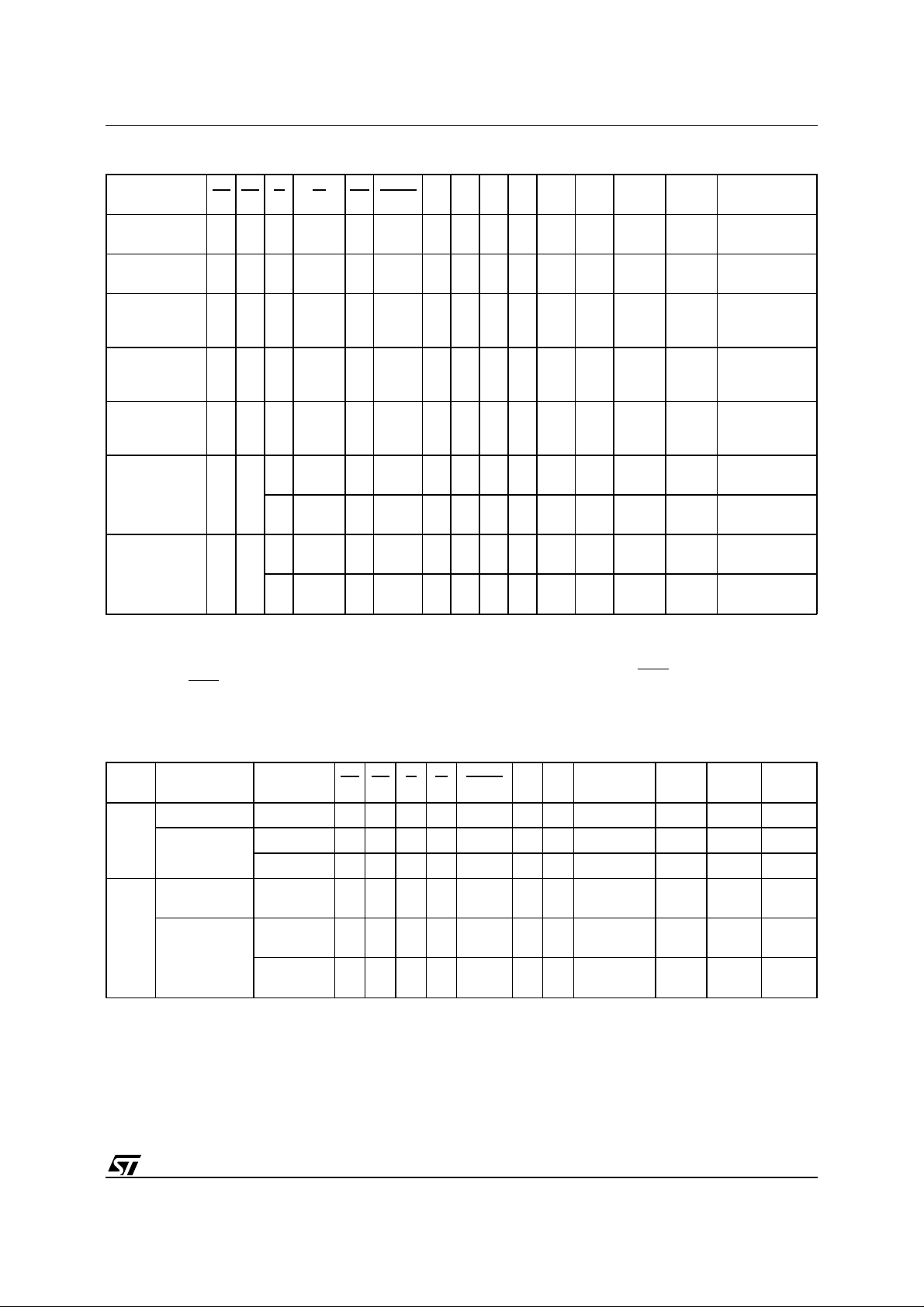
T ab le 6. User Bus Operations
(1)
Operation EE EF G W RP BYTE A0 A1 A6 A9 A12 A15
Block
Protection
(2,4)
Blocks
Unprotection
V
IH
VILV
V
IH
(4)
VIDV
V
IL
V
ID
Pulse
V
IL
ID
Pulse
X XXXVIDXX X X X
IH
V
X XXXVIDVIHV
IH
Block
V
Protection
(2,4)
Verify
Block
Unprotection
(2,4)
Verify
Block
Temporary
IH
VILVILV
V
IH
VILVILV
V
IH
XX X VIDX XXXX X X X X X
IHVIH
IHVIH
XVILVIHVILVIDA12 A15 X X
XVILVIHVIHVIDA12 A15 X X
Unprotection
V
VILVIHVILA0 A1 VILVIDXXA–1 X
Write the
EEPROM
Identifier
(5)
V
IL
Read the
V
EEPROM
Identifier
Notes:
(5)
1. X = V
2. Block Address must be given on A12-A18 bits.
3. See Table 8.
4. Operation performed on programming equipment.
5. The 65 Bytes User defined EEPROM Identifier are accessed on DQ0-DQ7 with A0 to A5 when
when
IL
or V
IL
IH
BYTE = 0 (x8)
V
V
IH
IH
IH
VILVIHVIHA0 A1 VILVIDXX X X
V
IH
VILV
V
IL
IHVIHVIL
V
IHVIHVIH
A0 A1 VILVIDXXA–1 X
A0 A1 VILVIDXX X X
DQ15
A–1
IH
DQ8-
DQ14
XX X
BYTE = 1 (x16) or with A–1 to A4
DQ0-DQ7
Block Protect
Block Protect
Status
Status
(3)
(3)
64 Bytes User
Defined
64 Bytes User
Defined
64 Bytes User
Defined
64 Bytes User
Defined
T able 7. Read Electronic Signature (following AS instruction or with A9 = VID)
Org. Code Device EE EF G W BYTE A0 A1
Word-
wide
Manufacturer V
Flash
M39832-T V
M39832-B V
Manufacturer V
IHVILVILVIH
IHVILVILVIH
IHVILVILVIH
IHVILVILVIH
V
VILV
IH
V
VIHVILDon’t Care 0 00h D7h
IH
V
VIHVILDon’t Care 0 00h 5Bh
IH
V
VILVILDon’t Care
IL
Byte-
wide
M39832-T V
IHVILVILVIH
V
VIHVILDon’t Care
IL
Flash
M39832-B V
IHVILVILVIH
V
VIHVILDon’t Care
IL
Other
Addresses
Don’t Care 0 00h 20h
IL
DQ15
A–1
Don’t
Care
Don’t
Care
Don’t
Care
DQ8-
DQ14
DQ0-
DQ7
Hi-Z 20h
Hi-Z D7h
Hi-Z 5Bh
11/36
Page 12

M39832
Table 8. Read Block Protection with AS Instruction (EF = 0, EE = 1)
Code E G W A0 A1 A12-A18
Protected Block V
Unprotected Block V
IL
IL
V
IL
V
IL
V
IH
V
IH
V
IL
V
IL
V
V
Block Address Don’t Care 01h
IH
Block Address Don’t Care 00h
IH
Table 9. Status Bit
DQ Name Logic Level Definition Note
Erase Complete or erase
block in Erase Suspend
Program Complete or data
of non erase block during
Erase Suspend
Erase Complete or Erase
Suspend on currently
addressed block
Indicates the P/E.C. status, check during
Program or Erase, and on completion
before checking bits DQ5 for Program or
Erase Success.
data on DQ6 while Programming or Erase
operations are on-going. DQ6 remains at
constant level when P/E.C. operations are
completed or Erase Suspend is
acknowledged.
This bit is set to ’1’ in the case of
Programming or Erase failure.
Data
7
Polling
6 Toggle Bit
5 Error Bit
4 Reserved
’1’
’0’ Erase On-going
DQ
DQ Program On-going
’-1-0-1-0-1-0-1-’ Erase or Program On-going Successive reads output complementary
DQ Program Complete
’-1-1-1-1-1-1-1-’
’1’ Program or Erase Error
’0’ Program or Erase On-going
Other
Addresses
DQ0-DQ7
Erase
3
Time Bit
’1’ Erase Timeout Period Expired
’0’
Erase Timeout Period
On-going
possible command entry is Erase Suspend
(ES).
An additional block to be erased in parallel
can be entered to the P/E.C.
Chip Erase, Erase or Erase
Suspend on the currently
P/E.C. Erase operation has started. Only
’-1-0-1-0-1-0-1-’
2 Toggle Bit
addressed block.
Erase Error due to the
currently addressed block
(when DQ5 = ’1’).
Indicates the erase status and allows to
identify the erased block
Program on-going, Erase
1
on-going on another block or
Erase Complete
DQ
Erase Suspend read on
non Erase Suspend block
1 Reserved
0 Reserved
Notes:
Logic level ’1’ is High, ’0’ is Low. -0-1-0-0-0-1-1-1-0- represent bit value in successive Read operations.
12/36
Page 13

Figure 4. EEPROM SDP Enable Flowcharts
M39832
Page
Write
Instruction
WRITE AAh in
Address 5555h
WRITE 55h in
Address 2AAAh
WRITE A0h in
Address 5555h
SDP is set
SDP ENABLE ALGORITHM
Page
Write
Instruction
SDP
Set
WRITE AAh in
Address 5555h
WRITE 55h in
Address 2AAAh
WRITE A0h in
Address 5555h
WRITE Data to
be Written in
any Address
Write
in Memory
SDP
not Set
WRITE
is enabled
Write Data
+
SDP Set
after tWC
AI01698B
A W rite operation can be used for two goals:
Write.
– either write data in the EEPROM memory array
– or enter a sequence of bytes or word composing
an instruction.
The reader should note that Programming a Flash
byte or word is an instruction (see Instructions
paragraph).
Writing data requires:
– the Chip Enable (either
– the Write Enable (
EE or EF) to be Low
W) to be Low with Output
Enable (G) High.
Addresses in Flash array (or EEPROM array) are
latched on the falling edge of
W or EF (EE) whichever occurs last; the data to be written in Flash
array (EEPROM array) is latched on the rising edge
W or EF (EE) whichever occurs first.
of
Specific Read and Write Operations.
Device
specific data is accessed through operations decoding the V
level applied on A9 and the logic
ID
levels applied on address inputs (A0, A1, A6).
These specific operations are:
– Read the Manufacturer identifier
– Read the Flash identifier
– Define and Read the Flash Block protection
status
– Read the EEPROM identifier
– Write the EEPROM identifier
Note: The OTP row (64 bytes) is accessed with a
specific software sequence detailed in the paragraph "Write in OTP row".
Instructions
An instruction is defined as a sequence of specific
Write operations. Each received byte or word is
sequentially decoded (and not executed as standard Write operations) and the instruction is executed when the correct number of bytes or word
are properly received and the time between two
consecutive bytes or words is shorter than the
time-out value.
The sequencing of any ins truction must be followed
exactly , any invalid combination of instruction bytes
or word or time-out between two consecutive by tes
or word will reset the device logic into a Read
memory state (when addressing the Flash array)
or directly decoded as a single operation when
addressing the EEPROM ar ray.
For efficient decoding of the instruction, the two first
bytes or words of an instruction are the coded
cycles and are followed by a command confirmation byte or word.
13/36
Page 14

M39832
Figure 5. EEPROM SDP disable Flowchart
WRITE AAh in
Address 5555h
WRITE 55h in
Address 2AAAh
WRITE 80h in
Page
Write
Instruction
Address 5555h
WRITE AAh in
Address 5555h
WRITE 55h in
Address 2AAAh
WRITE 20h in
Address 5555h
Unprotected State
after
tWC (Write Cycle time)
AI01699B
Figure 6. EEPROM and Flash Data Polling
Flowchart
START
READ DQ5 & DQ7
at VALID ADDRESS
DQ7
DATA
NO
DQ5
READ DQ7
DQ7
DATA
FAIL PASS
= 1
YES
=
NO
YES
YES
=
NO
AI01369
READ
Read operations and instructions can be used to:
– read the contents of the Memory Array (Flash
and EEPROM)
– read the status bits and identifiers.
Read data (Flash and EEPROM)
Both Chip Enable
G) must be low in order to read the data from the
(
EF (or EE) and Output Enable
memory.
Read the Manufacturer Identifier
The manufacturer’s identifier can be read with two
methods: a Read operation or a Read instruction.
Read Operation.
The manufacturer’s identifier can
be read with a Read operation with specific logic
14/36
levels applied on A0, A1, A6 and the V
level on
ID
A9 (See Table 7).
Read Instruction.
The manufacturer’s identifier
can also be read with a single read operation
immediatly following the AS instruction (See Table
5A and Table 7).
Read the Flash Identifier
The Flash identifier can be read with two methods:
a Read operation or a Read instruction.
Read Operation.
The Flash identifier can be r ead
with a single Read operation with specific logic
levels applied on A0, A1, A6 and the V
level on
ID
A9 (See Table 7).
Read Instruction.
The Flash identifier can also be
read with a single read operation immediatly following the AS instruction (See Table 5A and Table 7).
Page 15

M39832
Read the EEPROM Id entifier
The EEPROM identifier (64 bytes, user defined)
can be read with a single Read operation with A6
= ’0’ and A9 = V
(See Table 6).
ID
When accessing the 64 Bytes of EEPROM Identifier, the only LSB addresses are decoded. The LS B
addresses are A0 to A5 when
A–1 to A4 when
BYTE = ’0’ (x8). Each Byte o f th e
BYTE = ’1’ (x16) and
EEPROM identifier can be individually accessed in
read or write mode.
Read the OTP Row
The OTP row is mapped in the EEPROM array
EE = ’0’, EF = ’1’). Read of the OTP row (64 bytes)
(
is by an instruction (ROTP) composed of three
specific Write operations of data bytes at three
specific memory locations (each location in a different page) before reading the OTP row content
(See Table 5B).
When accessing the OTP row, only the LSB addresses are decoded and A6 must be ’0’. The LSB
addresses are A0 to A5 when
A–1 to A4 when
BYTE = ’0’ (x8).
BYTE = ’1’ (x16) and
Each Read of the OTP row has to be followed by
the (RT) Return instruction (See T able 5B).
Read the Flash Block Protection Status
Reading the Flash block protection status is by a
read operation immediatly following the AS instruction (See Table 5A and Table 8). A12-A18 define
the Flash block whose protection has to be verified. This Read operation will output a 01h if the
Flash block is protected and a 00h if the Flash block
is not protected.
The Flash block protection status can also be
verified with a single Read operation (see chapter:
Flash array specific features), with V
on A9 (See
ID
Table 6 and Table 8).
Read the Status Bits
The M39832 provides several Write operation
status flags which may be used to minimize the
application write (or erase or program) time. These
signals are available on the I/O port bits when
programming (or erasing) are in progress. I t should
be noted that the Ready/Busy pins also reflects the
status of the EEPROM Write and the Flash Programming/Erasing.
Data Polling flag, DQ7.
When Erasing or Programming into the Flash block (or when Writing into
the EEPROM block), bit DQ7 outputs the comple-
ment of the bit being entered for Programming/Writing on DQ7. Once the Program instruction or the Write operation is per formed, the true
logic value is read on DQ 7 (in a Read operation).
Flash memory block specific features:
– Data Polling is effective after the fourth W pulse
(for programming) or after the sixth W pulse (for
Erase). It must be performed at the address
being programmed or at an address within the
Flash sector being erased.
– During an Erase instruction, DQ7 outputs a ’0’.
After completion of the instruction, DQ7 will output the last bit programmed (that is a ’1’ after
erasing).
– if the byte to be programmed is in a protected
Flash sector, the instruction is ignored.
– If all the Flash sectors to be erased are pro-
tected, DQ7 will be set to ’0’ for about 100µs, and
then return to t he previous addressed byte. No
erasure will be performed.
– if all sectors are protected, a Bulk Erase instruc-
tion is ignored.
T oggle flag, DQ6.
The M39832 also offers another
way for determining when the EEPROM write or
the Flash memory Program instruction is completed. During the internal Write operation, the DQ6
will toggle from ’0’ to ’1’ and ’1’ to ’0’ on subsequent
attempts to read any byte of the memory, when
G , EE or EF is low.
either
When the internal cycle is completed the toggling
will stop and the data read on DQ0-DQ7 is the
addressed memory byte. The device is now accessible for a new Read or Write operation. The operation is completed when two successive reads yield
the same output data.
Flash memory block specific features:
a. The T oggle bit is effective after the fourth
(for programming) or after the sixth
W pulse
W pulse (for
Erase).
b. If the byte to be programmed belongs to a pro-
tected Flash sector, the instruction is ignored and:
– if all the Flash sectors selected for erasure
are protected, DQ6 will toggle to ’0’ for about
100µs, and then return to the previous addressed byte.
– if all sectors are protected, the Bulk Erase in-
struction is ignored.
15/36
Page 16

M39832
Figure 7A. Data T oggle Flowchart
START
READ
DQ5 & DQ6
DQ6
=
TOGGLE
NO
DQ5
= 1
READ DQ6
DQ6
=
TOGGLE
FAIL PASS
NO
YES
YES
NO
YES
Figure 7B. Flash ata Toggle Flowchart
START
READ
DQ2, DQ5 & DQ6
DQ2, DQ6
=
TOGGLE
NO
DQ5
= 1
READ DQ2, DQ6
DQ2, DQ6
=
TOGGLE
FAIL PASS
NO
YES
YES
NO
YES
AI01370
Tog gle Bit, DQ2 (Flash array only).
This toggle
bit, together with DQ6, can be used to determine
the device status during the Erase operations. It
can also be used to identify the block being erased.
During Erase or Erase Suspend a read from a block
being erased will cause DQ2 to toggle. A read from
a block not being erased will set DQ2 to ’1’ during
erase and to DQ2 during Erase Suspend. During
Flash Array Erase, a read operation will caus e
DQ2 to toggle as all blocks are being erased. DQ2
will be set to ’1’ during program operation and when
erase is complete. After erase completion and if the
error bit DQ5 is set to ’1’, DQ2 will toggle if the faulty
block is addressed.
Error flag, DQ5 (F lash block only).
This bit is set
to ’1’ by the internal logic when there is a failure of
programming, block erase, or chip erase that results in invalid data in the memory block. I n case of
an error in block erase or program, the block in
which the error occured or to which the programmed data belongs, must be discarded. The
AI01873
DQ5 failure condition will also appear if a user tries
to program a ’1’ to a location that is previously
programmed to ’0’. Other Blocks may still be used.
The error bit resets after a Read/Reset (RD) instruction. In case of success of Program or Erase,
the error bit will be set to ’0’ . when A0 is High with
A1 Low.
Erase Timer Bit, DQ3 (Flash array only).
This bit
is set to ’0’ by internal logic when the last block
Erase command has been entered to the Command Interface and it is awaiting the Erase start.
When the erase timeout period is finished, after
50ms to 90ms, DQ3 returns to ’1’.
WRITE a BY TE (o r a PAGE) in EEPROM
It should be noticed that writing in the EEPROM
array is an operation, it is not an instruction (as for
Programming a byte in the Flash array).
Write a Byte in EEPROM Array
A write operation is initiated when Chip Enable
is Low and Write Enable
W is Low with Output
EE
16/36
Page 17

M39832
Enable G High. Addresses are latched on the falling
edge of
W, EE whichever occurs last.
Once initiated, the write operation is internally
timed until completion, that is during a time t
.
W
The status of the write operation can be found by
reading the Data Polling and Toggle bits (as detailed in the READ chapter) or the ER
B output. This
Ready/Busy output is driven low from the write of
the byte being written until the completion of the
internal Write sequence.
Write a Page in EEPROM Array
The Page write allows up to 64 bytes within the
same EEPROM page to be consecutively latched
into the memory prior t o initiating a programming
cycle. All bytes must be located in a single pa ge
address, that is A6-A14 when
or A5-A13 when
BYTE is low (x8) must be the same
BYTE is high (x16)
for all bytes. Once initiated, the Page write oper ation is internally timed until completion, that is during a time t
WC
.
The status of the write operation can be seen by
reading the Data Polling and Toggle bits (as detailed in the READ chapter) or the ER
B output. This
Ready/Busy output is driven low from the write of
the first byte to be written until the completion of the
internal Write sequence.
A Page write is composed of successive Write
operations which must be sequenced within a time
period (between two consecutive Write operations)
that is smaller than the t
time exceeds the t
WLWL
value. If this period of
WLWL
value, the internal program-
ming cycle will start.
EEPROM Array Software Data Pr otection
A protection instruction allows the user to inhibit all
write modes to the EEPROM array: the Software
Data Protection (referenced as SDP in the following). The SDP feature is useful for protecting the
EEPROM memory from inadvertent write cycles
that may occur during uncontrolled bus conditions.
The M39832 is shipped as standard in the unprotected state meaning that the EEPROM memory
contents can be changed by the user. After the SDP
enable instruction, the device enters the Protect
Mode where no further write operations have any
effect on the EEPROM memory contents.
The device remains in this mode until a valid SDP
disable instruction is received whereby the device
reverts to the unprotected state.
T o enable the Software Data Protection, the device
has to be written ( with a Page Write) with three
specific data bytes at three specific memory locations (each location in a different page) as shown
in Figure 4 and Table 5B. This sequence provides
an unlock key to enable the write action, and, at the
same time, SDP continues to be set. Any further
Write in EEPROM when the SDP is set will use this
same sequence of three specific data bytes at three
specific memory locations followed by the bytes to
write. The first SDP enable sequence can be directly followed by the bytes to written.
Similarly, to disable the Software Data Protection
the user has to write specific data bytes into six
different locations with a Page Write addressing
different bytes in different pages, as shown in Figure 5 and Table 5B.
The Software Data Protection state is non-volatile
and is not changed by power on/off sequences. The
SDP enable/disable instructions set/reset an internal non-volatile bit and therefore will require a write
time t
, This Write operation can be monitored
WC
only on the T oggle bit (status bit DQ6) and the ER
pin. The Ready/Busy output is driven low from the
first byte to be written (that is the first Write AAh,
@5555h of the SDP set/reset sequence) until the
completion of the internal Write sequenc e.
Write OTP Row
Writing (only one time) in the OTP row (64 bytes)
is enabled by an instruction (WOTP) . This instruction is composed of three specific Write operations
of data bytes at three specific memory locations
(each location in a different page) followed by the
the data to store in the OTP row (refer to T able 5B ).
When accessing the OTP row, the only LSB addresses are decoded and A6 must be ’0’. The LSB
addresses are A0 to A5 when
A–1 to A4 when
BYTE = ’0’ (x8). Once at least one
BYTE = ’1’ (x16) and
Byte of the OTP row has been written (even with
FFh), the whole row becomes Read only.
Write the EEPROM Block Identifier
The EEPROM block identifier (64 Bytes) can be
written with a single Write operation with A6 = ’0’
and the V
level on A9 (see Table 6). When ac-
ID
cessing the 64 Bytes of EEPROM Identifier, the
only LSB addresses are decoded. The LSB addresses are A0 to A5 when
A-1 to A4 when
BYTE = ’0’ (x8). Each Byte of the
BYTE = ’1’ (x16) and
EEPROM identifier c an be individually ac cessed in
read or write mode.
PROGRAM in the Flash ARRAY
It should be noted that writing data into the
EEPROM array and the Flash array is not performed in a similar way: the Flash memory requires
an instruction (see Instruction chapter) for Erasing
and another instruction for Programming one (or
more) byte(s) or word(s), the EEPROM memory is
directly written with a simple operation (see Operation chapter).
B
17/36
Page 18

M39832
Program (PG) Instruction.
This instruction uses
four write cycles. Both for Byte-wide configuration
and for Word-wide configuration. The Program
command A0h is written to address AAA Ah in the
Byte-wide configuration or to address 5555h in the
Word-wide configuration on the third cycle after two
Coded cycles. A fourth write operation latches the
Address on the falling edge of
W or EF and the Data
to be written on the rising edge and starts the
internal operation. Read operations output the
Status Register bits after the programming has
started. Memory programming is made only by
writing ’0’ in place of ’1’. Status bits DQ6 and DQ7
determine if programming is on-going and DQ5
allows verification of any possible error. Programming at an address not in blocks being erased is
also possible during erase suspend. In this case,
DQ2 will toggle at the address being programmed.
Auto Select (AS) Instruction.
This instruction
uses the two Coded cycles followed by one write
cycle giving the command 90h to addr ess AAAAh
in the Byte-wide configuration or address 5555h in
the Word-wide configuration for command set-up.
A subsequent read will output the manufacturer
code and the device code or the block protection
status depending on the levels of A0 and A 1. T he
manufacturer code is output when the addresses
lines A0 and A1 are Low, the Flash code for Top
Boot or Bottom Boot is output when A0 is High with
A1 Low.
The AS instruction allows access to the block protection status. After giving the AS instruction, A0 is
set to V
with A1 at VIH, while A12-A18 define the
IL
address of the block to be verified. A read in these
conditions will output a 01h if the block is protected
and a 00h if the block is not protected.
The ERASE in the Flash ARRAY
Flash Array Erase (FAE) Instruction.
This instruction uses six write cycles. The Erase Set-up
command 80h is written to address AAAAh in the
Byte-wide configuration or the address 5555h in
the Word-wide configuration on the third cycle after
the two Coded cycles. The Flash Array Erase Confirm command 10h is similarly written on the sixth
cycle after another two Coded cycles. If the second
command given is not an erase confirm or if the
Coded cycles are wrong, the instruction aborts and
the device is reset to Read Array. It is not necessary
to program the array with 00h first as it will be done
automatically before erasing it to FFh. Read operations after the sixth rising edge of
W or EF output
the Status Register bits. During the execution of the
erase, Data Polling bit DQ7 returns ’0’, then ’1’ on
completion. The Toggle bits DQ2 and DQ6 toggle
during erase operation and stop when erase is
completed. After completion, the Status Bit DQ5
returns ’1’ if there has been an Erase Failure.
Block Erase (BE) Instruction.
This instruction
uses a minimum of six write cycles. The Erase
Set-up command 80h is written to address AAAh in
the Byte-wide configuration or address 5555h in
the Word-wide configuration on third cycle after the
two Coded cycles. The Block Erase Confirm command 30h is similarly written on the sixth cycle after
another two Coded cycles. During the input of the
second command an address within the block to be
erased is given and latched into the memory. Additional block Erase Confirm commands and block
addresses can be written subsequently to erase
other blocks in parallel, without further Coded cycles. The erase will start after the erase timeout
period (see Erase Timer Bit DQ3 description).
Thus, additional Erase Confirm commands for
other blocks must be given within this delay. The
input of a new Erase Confirm command will restart
the timeout period. The status of the int er nal timer
can be monitored through the level of DQ 3, if DQ3
is ’0’ the Block Erase Command has been given
and the timeout is running, if DQ3 is ’1’, the timeout
has expired and the Block(s) are being erased. If
the second command given is not an erase confirm
or if the Coded cycles are wrong, t he instruction
aborts, and the device is reset to Read Array. It is
not necessary to program the block with 00h as it
will be done automatically before erasing it to FFh.
Read operations after the sixth rising edge of
W or
EF output the Status Register bits.
During the execution of the erase , the memory
accepts only the Erase Suspend ES and Read/Reset RD instructions. Data Polling bit DQ7 returns ’0’
while the erasure is in progress and ’1’ when it has
completed. The Toggle bit DQ2 and DQ6 toggle
during the erase operation. They stop when erase
is completed. After completion the Status bit DQ5
returns ’1’ if there has been an erase failure. In such
a situation, the Toggle bit DQ2 can be used to
determine which block is not correctly erased. In
the case of erase failure, a Read/Reset RD instruction is necessary in order to reset the memory.
18/36
Page 19

Figure 8. Block Protection Flowchart
BLOCK ADDRESS
START
on A12 to A18
EE = V
IH
n = 0
G, A9 = VID,
EF = V
IL
Wait 4µs
W = V
IL
Wait 100µs
M39832
W = V
IH
G = V
IH
Wait 4µs
READ DQ0 at PROTECTION
ADDRESS: A0, A6 = VIL, A1 = VIH and
A12 to A18 DEFINING BLOCK
NO
DQ0
= 1
YES
A9 = V
IH
PASS
++n
= 25
A9 = V
FAIL
NO
YES
IH
AI00853
19/36
Page 20

M39832
Figure 9. Block Unprotecting Flowchart
START
EE = EF = V
A6, A12, A15 = V
G, A9 = V
Wait 4µs
EF, G, A9 = V
Wait 4µs
Wait 10ms
W = V
EF, G = V
Wait 4µs
n = 0
W = V
IH
IH
IL
IH
IH
IH
ID
Note:
20/36
NO LAST
1. A6 is kept at V
reads, A6 must be kept at V
during unprotection algorithm in order to secure best unprotection verification. During all other protection status
IH
++n
= 1000
YES
FAIL
IL
READ at UNPROTECTION
ADDRESS: A1, A6 = VIH, A0 = V
A12 to A18 DEFINING BLOCK
(see Note 1)
=
00h
YESNO
DATA
IL
and
INCREMENT
BLOCK
NO
BLOCK
YES
PASS
AI00850
.
Page 21

M39832
T able 10. AC Measurement Conditions
Input Rise and Fall Times
Input Pulse Voltages 0.V to V
Input and Output Timing Ref.
Voltages
10ns
≤
V
CC
CC
/ 2
Figure 10. AC Testing Input Out put Waveform
V
CC
VCC / 2
0V
AI00939
(1)
T ab le 11. Capacitance
Symbol Parameter Test Condition Min Max Unit
C
IN
C
OUT
Note:
1. Sampled only, not 100% tested.
Input Capacitance VIN = 0V 6 pF
Output Capacitance V
(TA = 25 °C, f = 1 MHz )
Figure 11. Output AC Testing Load Circuit
V
CC
I
OH
DEVICE
UNDER
TEST
I
OL
CL includes JIG capacitance
V
= 1.5V when the DEVICE
OUT
UNDER TEST is in the
Hi-Z output state.
= 0V 12 pF
OUT
1N914
1N914
CL = 30pF
AI00854
Erase Suspend (ES) Instruction.
The Block
Erase operation may be suspended by this instruction which consists of writing the command B0h
without any specific address. No Coded cycles are
required. It permits reading of data fr om another
block and programming in another block while an
erase operation is in progress. Erase suspend is
accepted only during the Block Erase instruction
execution. Writing this command during Erase
timeout will, in addition to suspending the erase,
terminate the timeout. The Toggle bit DQ6 stops
toggling when erase is suspended. The T oggle bits
will stop toggling between 0. 1ms and 15ms after
the Erase Suspend (ES) command has been written. The device will then automatically be set to
Read Memory Array mode. When erase is suspended, a Read from blocks being erased will
output DQ2 toggling and DQ6 at ’1’. A Read from
a block not being erased returns valid data. During
suspension the memory will respond only to the
Erase Resume ER and the Program PG instructions.
A Pr ogr am operation can be initiated during erase
suspend in one of the blocks not being erased. It
will result in both DQ2 and DQ6 toggling when the
data is being programmed. A Read/Reset command will definitively abort erasure and result in
invalid data in the blocks being er ased.
Erase Resume (ER) Instruction.
If an Erase Suspend instruction was previously executed, the
erase operation may be resumed by giving the
command 30h, at any address, and without any
Coded cycles.
FLASH ARRAY SPECIFIC FEATURES
Block Protection (See Figure 8).
Each block can
be separately protected against Program or Erase
on programming equipment. Block protection provides additional data security, as it disables all
program or erase operations. This mode is activated when both A9 and G are raised to V
and an
ID
address in the block is applied on A12-A18. Block
protection is initiated on the edge of W falling to V
IL
Then after a delay of 100ms, the edge of W rising
ends the protection operations. Block protec-
to V
IH
tion verify is achieved by bringing G,
and A1 to VIH, while W is at VIH and A9 at VID.
to V
IL
EF, A0 and A6
.
21/36
Page 22

M39832
Under these conditions, reading the data output will
yield 01h if the block defined by the inputs on
A12-A18 is protected. Any attempt to program or
erase a protected block will be ignored by the
device.
Remarks:
– The Verify operation is a read with a simulated
worst case conditions. This allows a guarantee
of the retention of the Protection status
– During the application life, the block protection
status can be accessed with a regular Read
instruction without applying a "high voltage" V
on A9. This instruction is detailed in T able 5 and
Table 8.
Blocks Unprotection (See Figure 9).
All protected
blocks can be unprotected simultaneously on programming equipment to allow updating of bit contents. All blocks must first be protected before the
unprotection operation. Block unprotection is activated when A9,
. Unprotection is initiated by the edge of W
at V
IH
falling to V
G and E are at VID and A12, A15
. After a delay of 10ms, the unprotection
IL
operation will end. Unprotection verify is achieved
by bringing
A1 are at V
G and E to VIL while A0 is at VIL, A6 and
and A9 remains at VID. In these
IH
conditions, reading the output data will yield 00h if
the block defined by the inputs A12-A18 has been
succesfully unprotected. Each block m ust be separately verified by giving its address in order to
ensure that it has been unprotected.
Remarks:
– The Verify operation is a read with a simulated
worst case conditions. This allows a guarantee
of the retention of the Protection status
– During the application life, the Block protection
status can be accessed with a regular Read
instruction without "high voltage" V
on A9. This
ID
instruction is detailed in Table 5 and Table 8.
Block Temporary Unprotection.
Any previously
protected block can be temporarily unprotected in
order to change stored data. The temporary unprotection mode is activated by bringing RP to V
ID
During the temporary unprotection mode the previously protected blocks are unprotected. A block
can be selected and data can be modified by
executing the Erase or Program instruction with the
RP signal held at V
. When RP is returned to VIH,
ID
all the previously protected blocks are again protected.
Read/Reset (RD) Instruction.
The Read/Reset
instruction consists of one write cycle giving the
command F0h. It can be optionally preceded by the
two Coded cycles. Subsequent read operations will
read the memory array addressed and output the
data read. A wait state of 10ms is necessary after
Read/Reset prior to any valid read if the memory
was in an Erase mode when the RD instruction is
given.
GLOSSARY
Array:
ID
EEPROM array (256 Kbit) or Flash array (8
Mbit)
part of the Flash array (See Figure 3A and
Block:
3B).
64 bytes of EEPROM
Page:
Write and Program:
Writing (into the EEPROM
array) and programming (the Flash array is not
performed in a similar way:
– the Flash memory requires an instruction (see
Instruction chapter) for Erasing and another instruction for Programming one (or more) byte(s)
or word(s)
– the EEPROM memory is directly written with a
simple operation (see Operation chapter).
Software Data Protection. Used for protect-
SDP:
ing the EEPROM array against false Write operations (as in noisy environments).
POWER SUPPLY and CURRENT CONSUMPTION
Power Up.
The M39832 internal logic is reset upon
a power-up condition to Read memory status. Any
Write operation in EEPROM is inhibited during the
first 5 ms following the power-up.
Either
EF, EE or W must be tied to VIH during
Power-up for the maximum security of the data
contents and to remove the possibility of a byte
being written on the first rising edge of
W. Any write cycle initiation is locked when Vcc is
below V
.
Supply Rails .
.
LKO
Normal precautions must be taken
for supply voltage decoupling, each device in a
system should have the V
0.1µF capacitor close to the V
rail decoupled with a
CC
and VSS pins. The
CC
printed circuit board trace width should be suff icient
to carry the V
program and erase currents re-
CC
quired.
EF, EE or
22/36
Page 23

M39832
T ab le 12. DC Characteristics
(T
= 0 to 70°C or –40 to 85°C; VCC = 2.7 to 3.6V)
A
Symbol Parameter Test Condition Min Max Unit
I
Note:
I
I
CC1
I
CC2
I
CC3
I
CC4
I
CC5
V
V
V
V
V
I
V
LO
LKO
Input Leakage Current 0V ≤ VIN ≤ V
LI
Output Leakage Current 0V ≤ V
(1)
Supply Current (Read Flash)
Supply Current (Read EEPROM)
EE = VIH, EF = VIL, G =
, f = 6MHz
V
IH
EE = VIL, EF = VIH, G =
V
, f = 6MHz
IH
OUT
≤ V
CC
CC
Supply Current (Standby) EF = EE = VCC ± 0.2V 100
Supply Current (Flash Block
Program or Erase)
Supply Current (EEPROM Write) During t
Input Low Voltage –0.5 0.8 V
IL
Input High Voltage 0.7 V
IH
Output Low Voltage IOL = 1.8mA 0.45 V
OL
Output High Voltage IOH = –100µAV
OH
A9 High Voltage 11.5 12.5 V
ID
VID Current A9 = V
ID
Byte program, Sector or
Chip Erase in progress
WC
ID
VCC Minimum for Write, Erase and
Program
1. When reading the Flash block when an EEPROM byte(s) is under a write cycl e, the supply cur rent is I
1
±
1
±
10 mA
10 mA
20 mA
20 mA
CC
–0.4 V
CC
VCC + 0.3 V
100
1.9 2.3 V
+ I
.
CC1
CC5
A
µ
A
µ
A
µ
A
µ
23/36
Page 24

M39832
Figure 12. Read Mode AC Waveforms
tEHFL
tEHQZ
tEHQX
tGHQZ
tGHQX
AI01952
VALID
tAVAV
VALID
A0-A18
tAVQV tAXQX
EE (EF)
tELQV
tEHFL
EF (EE)
tELQX
tGLQV
tGLQX
OUTPUT ENABLE DATA VALID
ADDRESS VALID
AND CHIP ENABLE
W) = High
G
DQ0-DQ7
Write Enable (
Note:
24/36
Page 25

T ab le 13. Read AC Characteristics
(T
= 0 to 70°C or –20 to 85°C; VCC = 3.3V ± 0.3V)
A
Symbol Alt Parameter Test Condition
M39832
-120 -150
Min Max Min Max
M39832
Unit
t
AVAV
t
AVQV
t
ELQX
t
ELQV
t
GLQX
t
GLQV
t
EHQX
t
EHQZ
t
GHQX
t
GHQZ
t
AXQX
t
RC
t
ACC
(1)
t
LZ
(2)
t
CE
(1)
t
OLZ
(2)
t
OE
t
OH
(1)
t
HZ
t
OH
(1)
t
DF
t
OH
Address Valid to Next
Address Valid
Address Valid to Output
Valid
Chip Enable Low to Output
Transition
Chip Enable Low to Output
Valid
Output Enable Low to
Output Transition
Output Enable Low to
Output Vali d
Chip Enable High to
Output Transition
Chip Enable High to
Output Hi-Z
Output Enable High to
Output Transition
Output Enable High to
Output Hi-Z
Address Transition to
Output Transition
(EE, EF) = (VIL, VIH) or
(EE, EF) = (VIH, VIL),
G = VIL
(EE, EF) = (VIL, VIH) or
(EE, EF) = (VIH, VIL),
G = VIL
G = V
IL
G = V
IL
(EE, EF) = (VIL, VIH) or
(EE, EF) = (VIH, VIL)
(EE, EF) = (VIL, VIH) or
(EE, EF) = (VIH, VIL)
G = V
IL
G = V
IL
(EE, EF) = (VIL, VIH) or
(EE, EF) = (VIH, VIL)
(EE, EF) = (VIL, VIH) or
(EE, EF) = (VIH, VIL)
(EE, EF) = (VIL, VIH) or
(EE, EF) = (VIH, VIL),
G = VIL
120 150 ns
120 150 ns
00ns
120 150 ns
00ns
55 55 ns
00ns
40 40 ns
00ns
40 40 ns
00ns
t
t
EHFL
Notes:
1. Sampled only, not 100% tested.
G may be delayed by up to t
2.
EE (EF) Active to EF (EE) 100 100 ns
CED
ELQV
- t
after the falling edge of EE (or EF) without increasing t
GLQV
ELQV
.
25/36
Page 26

M39832
Figure 13. Write AC Waveforms, W Controlled
WRITE CYCLE
A0-A18
(1)
E
G
W
DQ0-DQ7
RB
V
CC
tVCHEL
tAVWL
tELWL
VALID
tWLWHtGHWL
tDVWH
tWLAX
tWHEH
tWHGL
tWHWL
tWHDX
VALID
tWHRH
tWHRL
AI01953
Notes:
Address are latched on the falling edge of
E is either EF when EE = VIH or EE when EF = VIH.
26/36
W, Data is latched on the rising edge of W.
Page 27

Figure 14. Write AC Waveforms, E Controlled
M39832
WRITE CYCLE
A0-A18
W
G
(1)
E
DQ0-DQ7
DQ0-DQ7
RB
V
CC
tWLEL
tVCHWL
tAVEL
VALID
tELEHtGHEL
tDVEH
tELAX
tEHWH
tEHGL
tEHEL
tEHDX
VALID
tWHRL
AI01954
Notes:
Address are latched on the falling edge of
E is either EF when EE = VIH or EE when EF = VIH.
E, Data is latched on the rising edge of E.
27/36
Page 28

M39832
Table 14. Write AC Characteristics, Write Enable Contro lled
= 0 to 70°C or –40 to 85°C; VCC = 2.7V to 3.6V)
(T
A
Symbol Alt Parameter
t
AVAV
t
ELWL
t
WLWH
t
DVWH
t
WHDX
t
WHEH
t
WHWL
t
AVWL
t
WLAX
t
GHWL
t
VCHEL
t
WHQV1
t
WHQV2
(2)
(2)
t
Address Valid to Next Address Valid 120 150 ns
WC
t
Chip Enable Low to Write Enable Low 0 0 ns
CS
t
Write Enable Low to Write Enable High 50 65 ns
WP
t
Input Valid to Write Enable High 50 65 ns
DS
t
Write Enable High to Input Transition 0 0 ns
DH
t
Write Enable High to Chip Enable High 0 0 ns
CH
t
Write Enable High to Write Enable Low 30 35 ns
WPH
t
Address Valid to Write Enable Low 0 0 ns
AS
t
Write Enable Low to Address Transition 50 65 ns
AH
Output Enable High to Write Enable Low 0 0 ns
t
(1)
(1)
V
VCS
High to Chip Enable Low 50 50
CC
Write Enable High to Output Valid (Program) 15 15
Write Enable High to Output Valid
(Sector Erase)
M39832
-120 -150
Min Max Min Max
2.0 30 2.0 30 sec
Unit
s
µ
s
µ
t
WHWL0
t
t
WHGL
(3)
t
WHRL
Notes:
1. Time is measured to Data Polling or Toggle Bit, t
2. Chip Enable means (EE, EF) = (VIL, VIH) or (EE, EF) = (VIH, VIL).
3. With a 3.3KΩ pull-up resistor.
Time Out between 2 consecutive Section Erase 80 80
Write Enable High to Output Enable Low 0 0 ns
OEH
t
Write Enable High to Ready/Busy Output Low 150 150 ns
DB
WHQV
= t
WHQ7V
+ t
Q7VQV
s
µ
28/36
Page 29

M39832
T ab le 15. Write AC Characteristics, EE or EF Controlled
= 0 to 70°C or –40 to 85°C; VCC = 2.7V to 3.6V)
(T
A
Symbol Alt Parameter
t
WLWL
t
WHRH
t
t
WLEL
t
ELEH
t
DVEH
t
EHDX
t
EHWH
t
EHEL
t
t
ELAX
t
GHEL
t
VCHWL
t
EHQV1
AVAV
AVEL
t
Byte Load Cycle (EEPROM) 0.2 150 0.2 150
BLC
t
Write Cycle Time (EEPROM) 10 10 ms
WC
Address Valid to Next Address Valid 120 150 ns
t
Write Enable Low to Memory Block Enable Low 0 0 ns
WS
Memory Block Enable Low to Memory Block
t
CP
Enable High
t
Input Valid to Memory Block Enable High 50 65 ns
DS
t
Memory Block Enable High to Input Transition 0 0 ns
DH
t
Memory Block Enable High to Write Enable High 0 0 ns
WH
t
Memory Block Enable High to Memory Block
CPH
Enable Low
t
Address Valid to Memory Block Enable Low 0 0 ns
AS
t
Memory Block Enable Low to Address Transition 50 65 ns
AH
Output Enable High to Memory Block Enable Low 0 0 ns
t
VCC High to Write Enable Low 50 50
VCS
(1)
Memory Block Enable High to Output Valid
(Program)
M39832
-120 -150
Min Max Min Max
50 65 ns
30 35 ns
15 15
Unit
µ
µ
µ
s
s
s
(1)
t
EHQV2
t
EHGL
t
EHRL
Notes:
1. Time is measured to Data Polling or Toggle Bit, t
2. With a 3.3KΩ pull-up resistor.
t
(2)
Memory Block Enable High to Output Valid
(Sector Erase)
Memory Block Enable High to Output Enable Low 0 0 ns
OEH
EEPROM Block Enable High to Ready/Busy Output
t
DB
Low
WHQV
= t
WHQ7V
+ t
Q7VQV
2.0 30 2.0 30 sec
150 150 ns
.
29/36
Page 30

M39832
Figure 15. Data Polling DQ7 AC Waveforms
AI01955
READ CYCLE
DATA OUTPUT VALID
BYTE ADDRESS (WITHIN SECTORS)
tELQV
tAVQV
tEHQ7V
tGLQV
VALID
DQ7
tWHQ7V
VALID
tQ7VQV
IGNORE
DATA POLLING (LAST) CYCLE DATA VERIFY
READ CYCLES
DATA POLLING
.
IH
30/36
A0-A18
or E E when EF = V
IH
OR ERASE
LAST CYCLE
OF PROGRAM
is the Program or Erase time.
(5)
E
G
W
DQ7
DQ0-DQ6
WHQ7V
2. DQ7 and DQ0-DQ6 can transmi t to valid at any point during the data output valid period.
E is either EF when EE = V
3. t
4. During erasing operation Byte address must be within Sector being erased.
5.
1. All other timings are as a normal Read cyc le .
Notes:
Page 31

Ta ble 16. Data Polling and Toggle Bit AC Characteristics
= 0 to 70°C or –40 to 85°C; VCC = 2.7V to 3.6V)
(T
A
Symbol Parameter
Write Enable High to DQ7 Valid
WHQ7V1
t
WHQ7V2
t
EHQ7V1
t
EHQ7V2
(2)
(Program,
Write Enable High to DQ7 Valid
(2)
(Sector Erase,
Flash Block Enable High to DQ7 Valid
(2)
(Program,
Flash Block Enable High to DQ7 Valid
(2)
(Sector Erase,
W Controlled)
W Controlled)
EF Controlled)
EF Controlled)
t
M39832
(1)
M39832
-120 -150
Min Max Min Max
10 10
1.5 30 1.5 30 sec
10 10
1.5 30 1.5 30 sec
Unit
µ
µ
s
s
t
Notes:
Q7VQV
Q7 Valid to Output Valid (Data Polling) 50 55 ns
1. All other timings are defined in Read AC Characteristics table.
is the Program or Erase time.
2. t
WHQ7V
Tabl e 17. Program, Erase Times and Program, Erase Endurance Cycl es (Flash Block)
(T
= 0 to 70°C; VCC = 2.7V to 3.6V)
A
M39832
Parameter
Min Typ
Typical after
100k W/E Cycles
Max
Flash array Erase (Preprogrammed) 5 5 sec
Flash array Erase 12 12 sec
Flash array Block Erase 2.4 sec
Parameter Block Erase 2.3 sec
Main Block (32Kb) Erase 2.7 sec
Main Block (64Kb) Erase 3.3 15 sec
Chip Program (Byte) 8 8 sec
Byte Program 10 10
Word Program 20 20
Program/Erase Cycles (per Block) 100,000 cycles
Unit
s
µ
s
µ
31/36
Page 32

M39832
Figure 16. Data Toggle DQ6 AC Waveforms
AI01956
VALID
tEHQV
tAVQV
tELQV
tGLQV
VALID
tWHQV
STOP TOGGLE
VALID
IGNORE
READ CYCLE
READ CYCLE
DATA TOGGLE
.
IH
32/36
A0-A18
DATA
TOGGLE
READ CYCLE
OF ERASE
LAST CYCLE
OF PROGRAM
or E E when EF = V
IH
E is either EF when EE = V
1. All other timings are as a normal Read cyc le .
(2)
E
G
W
DQ6
DQ0-DQ5,
DQ7
2.
Notes:
Page 33

Figure 17. EEPROM Page Write Mode AC Waveforms, W Controlled
M39832
A0-A14
or A–1-A13
EE
G
W
DQ0-DQ7
ERB
tWLWH
Addr 0
tWHWL
Byte 0 Byte 1 Byte 2 Byte n
Addr 1 Addr 2 Addr n
tWLWL
tWHRL
tWHRH
AI00856
33/36
Page 34

M39832
ORDERING INFORMATION SCHEME
Example: M39832 - B 15 W NE 6 T
Array Matrix
T Top Boot
B Bottom Boot
Speed
12 120ns
15 150ns
Operating Voltage
W 2.7V to 3.6V
Package
NE TSOP48
12 x 20mm
Option
T T ape & Reel
Packing
Temp. Range
1 0 to 70 °C
6 –40 to 85 °C
Devices are shipped from the factory with the memory content set at all "1’s" (FFh).
For a list of available options (Speed, Package, etc...) or for further information on any aspect of this device,
please contact the STMicroelectronics Sales Office nearest to you.
34/36
Page 35

TSOP48 - 48 lead Plastic Thin Small Outline, 12 x 20mm
M39832
Symb
Typ Min Max Typ Min Max
A 1.20 0.047
A1 0.05 0.15 0.002 0.006
A2 0.95 1.05 0.037 0.041
B 0.17 0.27 0.007 0.011
C 0.10 0.21 0.004 0.008
D 19.80 20.20 0.780 0.795
D1 18.30 18.50 0.720 0.728
E 11.90 12.10 0.469 0.476
e 0.50 - - 0.020 - L 0.50 0.70 0.020 0.028
α
N48 48
CP 0.10 0.004
mm inches
0
°
5
°
0
°
5
°
Drawing is not to scale.
1 N
N/2
D1
DIE
TSOP-a
A2
e
E
B
A
D
CP
C
LA1 α
35/36
Page 36

M39832
Information furnished is believ ed to be accura te and reliable. Ho wever, STMicroelectronics as sum es no responsibility for the consequences
of use of such information nor for any infringement of patents or other rights of third parties which may result from its use. No license is granted
by implication or otherwise under any patent or patent rights of STMicroelectronics. Specifications mentioned in this publication are subject to
change without notice. This publication supersedes and repl aces all information previously supplied. STMicroelectron ics products are not
authorized for use as critical components in life support devices or systems without express written approval of STMicroelectronics.
The ST logo is a registered trademark of STMicroelect roni cs
© 1999 STMicroelectronics - All Rights Reserved
Australia - Brazil - Canada - China - France - Germany - Italy - Japan - Korea - Malaysia - Malta - Mexico - Morocco - The Netherlands -
Singapore - Spain - Sweden - Switzerland - Taiwan - Thailand - United Kingdom - U.S.A.
STMicroelectronics GROUP OF COMPANIES
http://www.st.com
36/36
 Loading...