

Page 1
Single Chip 4 Mbit Flash Memory and
■ Multiple Memories on a Single Chip:
– 4 Mbit Flash Memory (organised as 8 sectors)
– 256 Kbit EEPRO M
– 64 Byte One Time Programmable Memory
■ CONCURRENT Mode (Read Flash while
writing to EEPROM)
■ WRITE, PROGRAM and ERAS E Sta t u s Bits
■ 2.7V to 3.6V Single Supply Voltage for
PROGRAM, ERASE and READ Operat ions
■ 100 ns Access Time (Flash and EEPROM
blocks)
■ Low Power Consumption
–60µA Stand-by mode (maximum)
– Deep Power Down mode:
6 µA (maximum), 200 nA (typical)
■ Standard Flash Memory Package
■ 100,000 Erase/Write Cycles (minimum)
■ 10 Year Data Retention (minimum)
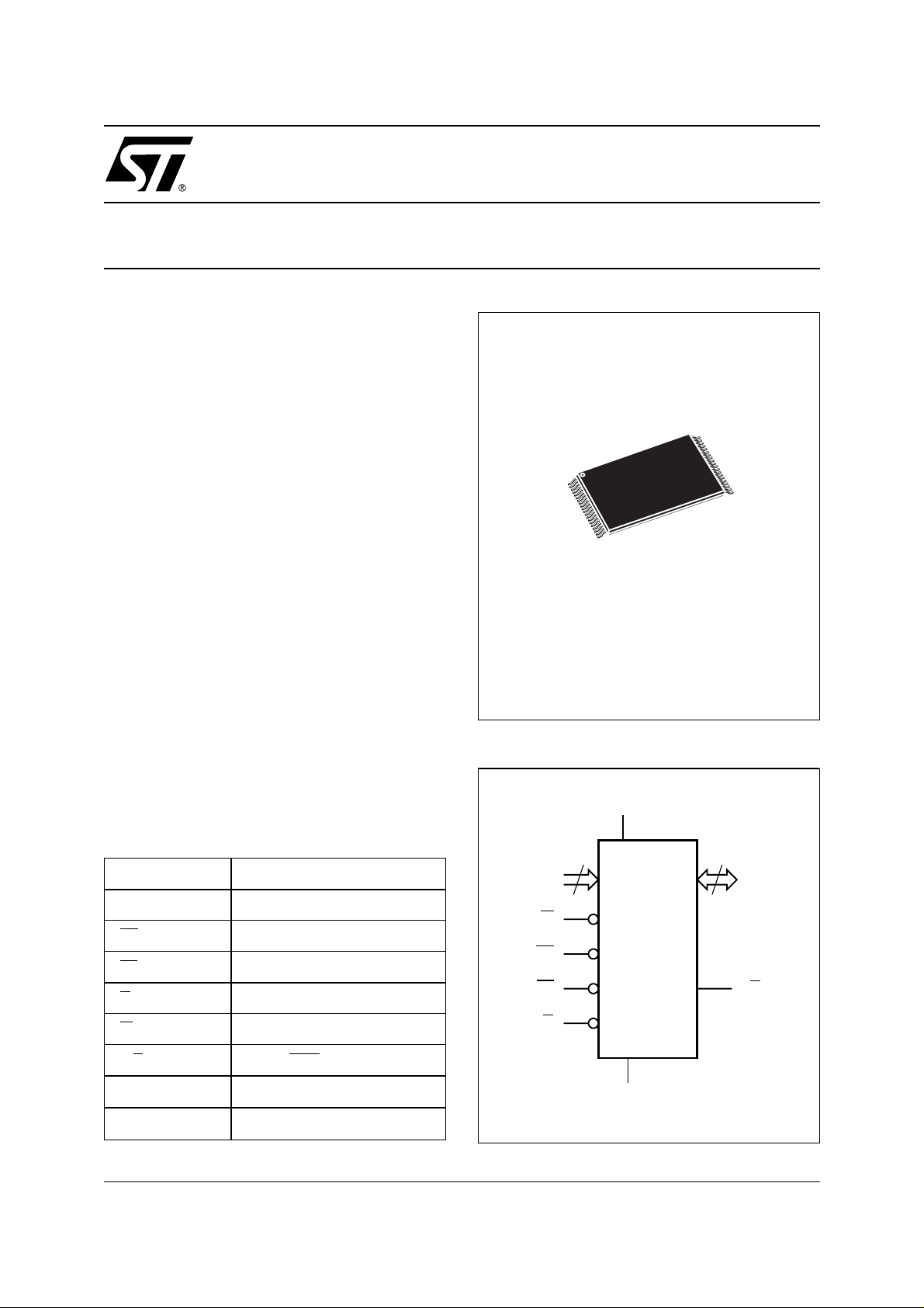
M39432
256 Kbit Parallel EEPROM
TSOP40 (NC)
10 x 20 mm
DESCRIPTION
The M39432 is a single supply voltage memory
device combining Flash memory and EEPROM on
a single chip. The memory is mapped in two
Table 1. Signal Names
A0-A18 Address Inputs
DQ0-DQ7 Data Inputs / Outputs
EE
EF
G
W
R/B
V
CC
V
SS
EEPROM Block Enable
Flash Block Enable
Output Enable
Write Enable
Ready/Busy Output
Supply Voltage
Ground
Figure 1. Logic Diagram
V
CC
19
A0-A18
W
EE
EF
G
M39432
V
SS
8
DQ0-DQ7
R/B
AI01946
1/28November 1999
Page 2
M39432
Figure 2. TSOP Connection s
NC
NC
A11
A9 A10
A8 EF
A13
A14
A17
V
CC
A18
A16
A15
A12
A7
A6 A1
A5 A2
A4
NC
NC
Note: 1. NC = Not Connected.
1
W
10
11
20 21
M39432
40
31
30
AI01947
NC
EE
G
DQ7
DQ6
DQ5
DQ4
DQ3
V
SS
DQ2
DQ1
DQ0
A0
A3
R/B
NC
blocks: 4 Mbit of Flash memory and 256 Kbit of
EEPROM. Each block operates independently
during a Write cycle: in concurrent mode, the
Flash Memory can be read while the EEP ROM is
being written.
There is also a 64 byte row of OTP (one time
programmable) EPROM.
The M39432 EEPROM block may be written
bytewise or by a page at a time (up to 64 bytes).
The integrity of the data can be s ecured with the
help of the Software Data Protection (SDP).
The M39432 Flash Memory block offers 8 sectors,
each one 64 KByt e in size. Each sector may be
erased individually, and programmed a byte at a
time. Each sector can be separately protected and
unprotected against Program and Erase. Sector
erasure may be suspended, while data is read
from other sectors of the Flash memory block (or
from the EEPR O M block), and then resumed. The
Flash memory block is functionally compatible with
the M29W040 (4 Mbit Single Voltage Flash
Memory).
During a Program or Erase cycle in the Flash
memory or during a Write cycle in the EEPROM,
the status of the M39432 internal logic can be read
on the Data Output pins DQ7, DQ6, DQ5 and
DQ3.
SIGNAL DESCRIPTION
Address Inputs (A0-A18)
The address inputs for the memory array are
latched during a write operation. The EEPROM
block is selected by the E E
memory block the EF
input, and the Flash
input. A0-A14 access
locations in the EEPROM block; A0-A18 access
locations in the Flash memory block.
When V
(as specified in Table 11) is applied on
ID
the A9 address input, additional device-specific
information can be accessed:
– Read the Manufacturer identifier
– Read the Flash block identifier
– Read/Write the EEPROM block identifier
– Verify the Flash Sector Protection Status.
Table 2. Absolute Maximum Ratings
Symbol Parameter Value Unit
T
A
T
BIAS
T
STG
1,2
V
IO
1
V
CC
, VG, VEF
V
A9
Note: 1. Stresses above those listed may cause permanent damage to the device. These are stress ratings only and operation of the device
2/28
at these or any oth er conditi ons abov e those indi cated in th e Operating sections of this spec ificatio n is not imp lied. Expo sure to
Absolute Maximum Rating conditions for extended periods may affect device reliability. Please see the STMicroelectronics SURE
Program an d ot her releva nt quality documents.
2. Minimum voltage ma y undershoot to –2 V, during transiti on and for less than 20 ns.
Ambient Operating Temperature –40 to 85 °C
1
Temperature Under Bias –50 to 125 °C
1
Storage Temperature –65 to 150 °C
Input or Output Voltage (except A9) –0.6 to 7 V
Supply Voltage –0.6 to 7 V
1,2
A9, G and EF Voltage –0.6 to 13.5 V
Page 3
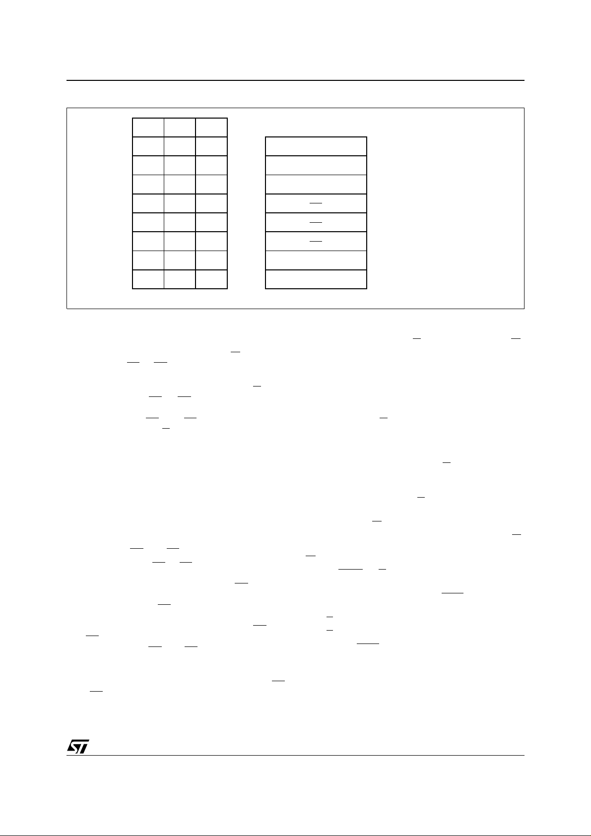
Figure 3. Flash Block Sectors
A18
A17
A16
TOP
ADDRESS
M39432
BOTTOM
ADDRESS
1
1 64K Bytes Block
1
1
0
0
001
000
AI01362B
1
1
0
0
1
1
1
0
1
0
1
0
Data Input/Output (DQ0-DQ7)
During a Write operation, one data byte is latched
into the device when Write E nable (W
Chip Enable (EF
or EE) are driven low.
) and one
During a Read operation, the output presented on
these pins is valid when Output Enable (G
one Chip Enable (E F
or EE) are driven low. The
) and
output is high impedance when the chip is
deselected (both EE
outputs are disabled (G
and EF driven high) or the
driven high).
Read operations are used to output:
– bytes in the Flash memory block
– bytes in the EEPROM block
– the Manufacturer Identifier
– the Flash Sector Protection Status
– the Flash Block Identifier
– the EEPROM Identifier
– the OTP row.
Chip Enable (EE
Each Chip Enable (EE
and EF)
or EF) causes the memory
control logic, input buffers, decoders and sense
amplifiers to be activated. When the EE
input is
driven high, the EEPROM memory block is not
selected; when the EF
input is driven high, the
Flash memory block is not sele cted. Attempts to
access both EEPROM and Flash blocks (EE
and EF
two chip enables (EE
low) are forbidden. Switching between the
and EF) must not be made
low
on the same clock cycle, a delay of greater than
must occur.
t
EHFL
The M39432 is in stand-by mode when both EF
and EE are high (when no internal Erase or
programming cycle is running). The power
consumption is reduced to the st and-by level and
64K Bytes Block
64K Bytes Block
64K Bytes Block
64K Bytes Block
7FFFFh
6FFFFh
5FFFFh
4FFFFh
3FFFFh
2FFFFh
1FFFFh
0FFFFh
70000h
60000h
50000h
40000h
30000h
20000h
10000h
00000h
the outputs are held in the high state, independent
of the Output Enable (G
) or Write Enable (W)
inputs.
After 150 ns of inactivity, and when the addresses
are driven at CMOS levels, the chip aut om atically
enters a pseudo-stand-by mode. Power
consumption is reduced to the CMOS stand-by
level, while the outputs continue to drive the bus.
Output Enable (G
)
The Output Enable gat es the outputs throug h the
data buffers during a Read operation. The data
outputs are left floating in their high impedance
state when the Output Enable (G
) is high.
During Sector Protect (Figure 8) and Sector
Unprotect (Figure 9) operations (for the Flash
memory block only), the G
(as specified in Table 11).
V
ID
Write Enable (W
)
input must be held at
Addresses are latched on the falling edge of W
and Data Inputs are latched on the rising edge of
W
.
Ready/Busy
(R/B )
When the EEPROM block is engaged in an
internal Wri te cycle, the Re ady/Busy
outp ut show s
the status of the device:
–R/B
is 0 when a Write cycle is in progress
is Hi-Z when no Write cycle is in progress
–R/B
The Ready/Busy
pin does not show the status of a
Program or Erase cycle in the Flash memory.
This pin can be used to show the status of the
EEPROM block, even when reading data (or
fetching instructions) from the Flash memory
block.
,
3/28
Page 4
M39432
Table 3. Operations
Operation EF EE G W DQ0 - DQ7
Read
Write
Output Disable
Stand-by
Note: 1. X = VIH or VIL.
V
IL
V
IH
V
IL
V
IH
V
IL
V
IH
V
IH
V
IH
V
IL
V
IH
V
IL
V
IH
V
IL
V
IH
V
IL
V
IH
V
IH
X X Hi-Z
V
IH
V
IL
X Hi-Z
Read from Flash Block
Read from EEPROM Block
Write to Flash Block
Write to EEPROM Block
This open drain output can be wire-ORed, using
an external pull-up resistor, when several M39xxx
devices are used together.
Supply Voltage
V
CC
The V
Supply Voltage supplies the power for
CC
the device. The M39432 cannot be written when
the V
Voltage, V
Supply Voltage is less than the Lo ckout
CC
. This prevents Bus Write operations
LKO
from accidentally damaging the data during power
up, power down and during power surges.
A 100 nF capacitor should be connected between
the V
Supply Voltage pin and the VSS Ground
CC
pin, to decouple the current surges from the power
supply. The PCB track widths must be sufficient to
carry the currents required during program and
erase operations.
Ground
V
SS
The V
Ground is the reference for all voltage
SS
measurements.
DEVICE OPERATION
The M39432 memory d evice is addressed via 19
inputs (A0-A18) and carries data on 8 Data Inputs/
Outputs (DQ0-DQ7). There are f our other control
inputs: Chip Enable EEPROM (EE
Flash Memory (EF
Enable (W
).
), Output Enable ( E) and Write
The Chip Enable inputs (EF
), Ch ip Enab le
or EE) are used
mainly for power control (turning the chip on and
off) and for block selection (selecting the
EEPROM block or the Flash memory block). The
gating of data to the DQ0-DQ7 pins should be
controlled using the Output Enable input (G
).
The permitted operating modes of the device are
listed in Table 3.
Read
For a Read operation, the Output Enable (G
one Chip Enable (EF
or EE) must be driven low.
) and
As noted on the previous page, Read operations
are used to read the contents of:
– bytes in the Flash memory block
– bytes in the EEPROM block
– the Manufacturer Identifier
– the Flash Sector Protection Status
– the Flash Block Identifier
– the EEPROM Identifier
– the OTP row.
The instruction sequences for selecting between
these areas is summarized in Table 4.
Write
Writing data requires:
– a Chip Enable (either EE
– the Write Enable (W
Enable (G
) to be high.
or EF) to be low
) to be low and the Output
Addresses in the Flash memory block (or the
EEPROM block) are latched on the falling edge of
or EF (or E E) whichever occurs the later. The
W
data to be written to the Flash memory block (or
EEPROM block) is latched on the rising edge of W
or EF (or EE) whichever occurs first.
The Write operation is used in two contexts:
– to write data to the EEPROM memory block
– to enter the sequ ence of bytes that makes up
one of the instructions shown in Table 4.
The programming of a byte of Flash memory
involves one of these instructions (as described in
the section entitled “Instructions” on this page).
Specific Read and Write Operations
Device specific information includes the following:
– Read the Manufacturer Identifier
– Read the Device Identifier
– Define the Flash Sector Protection
– Read the EEPROM Iden tifier
– Write the EEPROM Identifier
4/28
Page 5
M39432
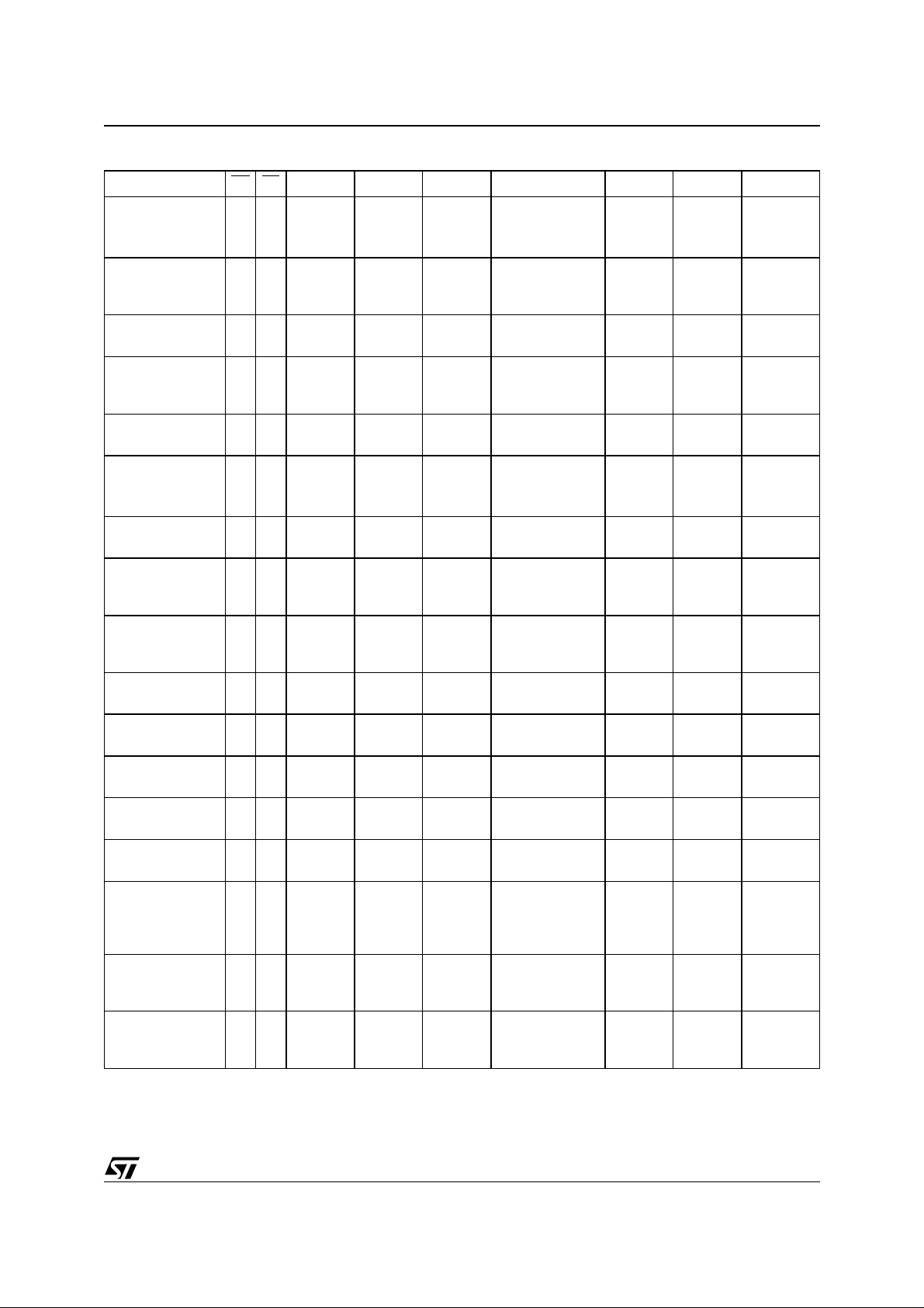
Table 4. Instructions
1
Instruction EE EF Cycle 1 Cycle 2 Cycle 3 Cycle 4 Cycle 5 Cycle 6 Cycle 7
Read
Manufacturer
Identifier
2
Read Flash
Identifier
2
10
10
Read OTP Row 0 1
Read Sector
Protection Status
Program a Byte of
Flash Memory
Erase a Sector of
Flash Memory
Erase the Whole
of Flash Memory
Suspend Sector
Erase
Resume Sector
Erase
10
2
10
10
10
10
10
AAh
@5555h
AAh
@5555h
AAh
@5555h
AAh
@5555h
AAh
@5555h
AAh
@5555h
AAh
@5555h
B0h
@any
address
30h
@any
address
55h
@2AAAh
55h
@2AAAh
55h
@2AAAh
55h
@2AAAh
55h
@2AAAh
55h
@2AAAh
55h
@2AAAh
90h
@5555h
90h
@5555h
90h
@5555h
90h
@5555h
A0h
@5555h
80h
@5555h
80h
@5555h
Read Identifier
with (A0,A1,A6)
set to (0,0,0)
Read Identifier
with (A0,A1,A6)
set to (1,0,0)
Read
Byte 1
Read Identifier
with (A0,A1,A6)
set to (0,1,0)
Data
@ Address
AAh
@5555h
AAh
@5555h
Read
Byte 2
55h
@2AAAh
55h
@2AAAh
30h
@ Sector
address
10h
@5555h
Read
Byte N
30h
@ Sector
address
3
EEPROM Power
Down
Deep Power
Down
SDP Enable
(EEPROM)
SDP Disable
(EEPROM)
01
10
01
01
Write OTP Row 0 1
Return (from OTP
Read or
EEPROM Power
01
Down)
Reset 1 0
Reset (short
instruction)
Note: 1. AAh @ 5555h means “Write the value AAh at the address 5555h”.
2. This instruction can also be performe d as a Verify operatio n wi t h A9=V
and Unprotection” on page 18).
3. Addresses of additio nal sectors to be erased must be entered wit hi n a time- out of 80 µs of each other.
10
AAh
@5555h
20h
@5555h
AAh
@5555h
AAh
@5555h
AAh
@5555h
F0h
@any
address
AAh
@5555h
F0h
@any
address
55h
@2AAAh
55h
@2AAAh
55h
@2AAAh
55h
@2AAAh
55h
@2AAAh
30h
@5555h
A0h
@5555h
80h
@5555h
B0h
@5555h
F0h
@any
address
Write
Byte 1
AAh
@5555h
Write
Byte 1
(please see the section entitl ed “Flash Sector Prot ection
ID
Write
Byte 2
55h
@2AAAh
Write
Byte 2
Write
Byte N
20h
@5555h
Write
Byte N
5/28
Page 6
M39432
Table 5. Device Identifier Operations
Instruction EF EE G W A0 A1 A6 A9
Read Manufacturer
Identifier
Read Flash Block
Identifier
Read EEPROM
Block Identifier
Note: 1. X = Don’t Care.
V
V
V
IL
V
V
IL
V
IH
V
IH
IH
IL
V
IL
V
V
IL
V
V
IL
V
IH
V
IH
IH
V
IL
IL
V
IH
XX
IL
V
IL
V
IL
V
IL
V
ID
V
ID
V
ID
Other Address
Lines
Don’t Care 20h
Don’t Care 0E3h
Don’t Care
DQ0 - DQ7
defined bytes
64 user-
To access these, A9 is held at VID (as specified in
Table 11) and the specific logic le vels, shown in
Table 5, are applied to the address input s A0, A1
and A6.
The OTP row is accessed with a specific software
sequence, as described in the section entitled
“Writing the OTP Row” on page 11.
Instructions
Instructions consist of a sequence of specific Write
operations, as summarized in Table 4. The time
between two consecutive bytes must be shorter
than the time-out value (t
WLWL
).
Each received byte i s decoded sequent ially, and
not executed as a standard Write ope ration. The
overall instruction is executed when the correct
number of bytes have been properly received.
The sequence must be followed exactly. If an
invalid combination of instruction bytes occurs, or
time-out between two consecutive bytes, the
device logic resets itself to the Read state, when
addressing the Flash block, or is di rectly de coded
as a single operation, when addressing the
EEPROM block.
The M39432 instructions set, as summarized in
Table 4, includes:
■ Program a byte in the Flash memory block
■ Read the Protection Status of a Flash Sector
■ Erase instructions:
– Flas h Secto r Er a s e
– Flash Block Erase
– Flash Sector Erase Suspend
– Flash Sector Erase Resume
■ EEPROM Power Down
■ Deep Power Down
■ Change the EEPROM software write protection:
– Enable SDP
–Disable SDP
■OTP row access:
– Write the whole OTP row (once)
– Read from the OTP row
■ Reset and Return
■ Read identifiers:
– Read the Manufacturer Identifier
– Read the Flash Block Identifier
For efficiency, each instruction consists of a twobyte escape sequence, followed by a command
byte or a confirmation byte. The escape sequence
consists of writing the value AAh at address
5555h, in the first cycle, and the value 55h at
address 2AAAh, in the second cycle.
In the case of the Erase instructions, an additional
escape sequence is required, for final confirmation
that the instruction is the intended one.
POWER SUPPLY AND CURRENT
CONSUMPTION
Power Up
The M39432 internal logic is reset, to Read mode,
upon a power-up event. All Write operations to the
EEPROM are inhibited for the first 5 ms.
No new Write cycles can be started wh en V
below V
(as specified in Table 11). Howeve r,
LKO
CC
is
for maximum security of the contents of the
memory, and to remove the possibility of a byte
being written on the first rising edge of EF
, at least one of EF, E E or W should be tied to
W
V
during the power-up process.
IH
, EE or
Stand-by
When both EE
and EF are high, the memory
enters Stand-by mode, and the Dat a In put/Ou tput
pins are placed in the high-impedan ce state. To
reduce the Supply Current to the Stand-by Supply
Current, EE
V
±0.2V.
CC
and EF should be held within
If the Stand-by mode is set during a Program or
Erase cycle, the memory continues to use the
Supply Current until the cycle is complete.
6/28
Page 7
Table 6. Status Bits
EF EE DQ7 DQ6 DQ5 DQ4 DQ3 D Q2 DQ1 DQ0
Flash
EEPROM
Note: 1. X = Not a guaranteed v al ue, can be rea d ei ther as ‘1’ or ‘0 ’ .
V
IL
V
IH
V
V
Data
IH
Polling
Data
IL
Polling
Toggle
Flag
Toggle
Flag
M39432
Error
Flag
XXXXXX
Erase
X
Time-
Out
XXX
Automatic Stand-by
If CMOS le vels (V
±0.2V) are used to drive the
CC
bus, and the bus is inactive f or m ore t han 1 50 ns,
the memory enters the Automatic Stand-by state.
The internal supply current is reduced to the
Stand-by Supply Current, I
CC3
.
Deep Power Down
The I
consumption m ode can be reduced to a
CC
minimum using the Deep Power Down i nstruction
(as shown in Table 4). The device is set in a sleep
mode until the next Reset instruction is executed.
EEPROM Power Down
The M39432 can power-down the EEPROM block
using the specific instruction shown in Table 4.
Once in this state, the EEPROM block is no longer
accessible, until a Return instruction is executed.
READ
Read operations and instructions can be used:
– to read the contents of the memory array (Flash
memory block or EEPROM block)
– to read the memory array statu s and identifiers
(Flash memory block or EEPROM block).
Read Data (from Flash Memory or EEPROM)
For a Read operation, the Output Enable (G
one Chip Enable (EF
or EE) must be driven low.
) and
Read the Manufacturer Identifier
There are two alternative methods for reading the
Manufacturer Identifier: using a Read operation or
using a Read instruction.
Read Operation.
be read with a Read operation by applying V
The Manufacturer Identifier can
(as
ID
specified in Table 11) on A9, and t he logic levels
specified in Table 5 applied to A0, A1, A6.
Read Instruction.
The Manufacturer Identifier can
also be read using an instruction composed of four
operations: three specific Write operations (as
specified in Table 4) and a Re ad operation. This
either accesses the Manufacturer Identifier, the
Flash Block Identifier or the Flash Sector
Protection Status, depending on the levels that are
being applied to A0, A1, A6, A16, A17 and A18.
Read the Flash Block Identifier
Similarly, there are two alternative methods for
reading the Flash Block Identifier (E3h): using a
Read operation or using a Read instruction.
Please see the previous section, entitled “Read
the Manufacturer Identifier”, and Table 5 and
Table 4 for details.
Read the EEPROM Block Identifier
The EEPROM Block Identifier (64 bytes, user defined) can be read with a single Read operation by
holding A6 low and A9 at VID (see Table 5).
Read the OTP Row
The OTP row is mapped in the EEPROM block.
With EE
held low, and EF held high, an EEPROM
Read instruction is composed, as specified in
Figure 4. Dat a Po ll i ng F lo wc h a rt
START
READ DQ5 & DQ7
at VALID ADDRESS
DQ7
DATA
NO
DQ5
READ DQ7
DQ7
DATA
FAIL PASS
= 1
YES
=
NO
YES
YES
=
NO
AI01369B
7/28
Page 8
M39432
Table 4. This consists of the writing of three
specific data bytes at three specific memory
locations (each location on a different page) as a
prefix to reading the OTP row content.
When accessing the OTP row, only the least
significant bits of the address bus (A0 to A6) are
decoded (of which A6 must be low).
Each Read of the OTP row has t o be followed by
the Return instruction (as shown in Table 4).
Read the Flash Sector Protection Status
There are two alternative methods for reading the
Flash Sector Protection Status: using a Verify
operation with A9=V
(as described on page 18)
ID
or using a Read instruction as described in the
section entitled “Read the Manufacturer Identifier”,
starting on page 7.
Using the Read instruction, the logic levels on A0,
A1, A6 select the correct instruction, while A16,
A17 and A18 specify which sector is being
addressed. This returns the value 01h if the Flash
sector is protected, and the value 0 0h if t he F lash
sector is not protected.
Read the Status Bits
The latency period of W rite, Erase and Program
cycles can be monitored by the application
software, by using the M39432 status bits. The
Ready/Busy
pin provides the status information
during a write cycle to the EEPROM block (t hough
not to the Flash memory block). An internal status
register carries the status information during a
programming or erase cycle. A Read operation,
during the program or write cycle, causes the
contents of this register to be presented to the I/O
ports (DQ0-DQ7), as summarized in Table 6.
Data Polling flag, DQ7. The I/O lines (DQ0DQ7) are first used as inputs, carrying the data
that is to be written to the EEPROM or
programmed in the Flash memory. Once the Write
or Program cycle is underway, these lines become
outputs (and can be read using a normal Read
operation). The value presented on DQ7 is the
inverse of the data bit that was presented by the
user. When the cycle is complete, the lines remain
as outputs, and the value that is presented on DQ7
is the non-inverted value that was originally
specified for writing.
The suitable algorithm for using this method of
polling is shown in Figure 4. When a Write or
Program cycle is in progress, data bit DQ7 is set to
the complement of the original data bit 7 (or to ‘0’
in the case of an Erase cycle in the Flash memory
block). When DQ7 is identical to the old data (or to
‘1’ in the case of an Erase cycle in the Flash
memory block) and the Error bit (DQ5) is still ’0’,
the cycle is complete .
For the flash memory block, data Polling is
effective after the fourth pulse on the W
line for
Figure 5. Dat a Toggle Flow c hart
START
READ
DQ5 & DQ6
DQ6
=
TOGGLE
NO
DQ5
= 1
READ DQ6
DQ6
=
TOGGLE
FAIL PASS
NO
YES
YES
NO
YES
AI01370
Program cycles, and af ter the si xth pulse on th e W
line for Erase cycles. The Data Polling Read
instruction must address the same location as the
byte that is being programmed, or within the same
Flash sector as the one that is being erased.
Toggle flag , DQ6. During an internal Write,
Program or Erase cycle, DQ6 toggles between ’0’
and ’1’, on successive Read accesses to any byte
of the memory (when either G
, EE or EF is held
low).
When the internal cycle is complete, the toggling is
stopped, and the data read on DQ0-DQ7 is that of
the addressed memory byte. A subsequent
Reading at the same address will result in the
same data being read.
This alternative method for detecting when the
internal Write, Program or Erase cycle has
completed, is shown in the flowchart in Figure 5.
When an internal cycle is in progress, data bit DQ6
toggles between ‘1’ and ‘0’ for successive Read
operations. When DQ6 no longer toggles and the
Error bit DQ5 is ’0’, the operation i s complete. To
determine if DQ6 has toggled, each poll requires
two consecutive Read operations to see if the data
read is the same each time.
For the flash memory block, data Toggling is
effective after the fourth pulse on the W
line for
8/28
Page 9
M39432
Table 7. Summary of the Use of Status Bits
Operation Address
DQ7 (Data
Polling Bit)
DQ6 (Toggle Bit)
Program (Flash)
or
Any address DQ7
Toggling 0 X
Erase (EEPROM)
Program Error
(Flash)
Flash Block Erase
Sector Erase
Sector Erase
before Time-Out
Any address in
the Flash block
Any address in
the Flash block
Sector address to
be erased
Sector address to
be erased
DQ7
0
0
0
Toggling 1 X
1
1
1
Toggling
Toggling
Toggling
2
2
2
Any byte in the
sector in erase
Erase Suspend
Erase Error Sector address
Note: 1. If all the sectors to be erased are protected, DQ7 is reset to 0 for about 100 µs, then returns to the state it was in for the previously
addressed byte. No erasure is perf orm ed.
2. If all the sectors to be erased are protected, DQ6 is reset to 0 for about 100 µs, then returns to the state it was in for the previously
addressed byte. No erasure is perf orm ed.
mode
Other sector
addresses
DQ6 toggles for 15 µs, then behaves as for a standard Read operaion
1
0
Invalid data on DQ7-DQ0
Toggling
2
DQ5 (Program
Error Bit)
DQ3 (Erase
Time-Out Bit)
01
01
00
11
Figure 6. EEPROM SDP-Enable Flowcharts
Write AAh in
Address 5555h
Page Write
Timing
Write 55h in
Address 2AAAh
Write A0h in
Address 5555h
SDP is set
SDP ENABLE ALGORITHM
Page Write
Timing
SDP
Set
Write AAh in
Address 5555h
Write 55h in
Address 2AAAh
Write A0h in
Address 5555h
Write Data to
be Written in
any Address
Write
in Memory
SDP
not Set
Write Data
and
SDP Set
after t
WC
Write
is enabled
AI01698C
9/28
Page 10

M39432
Program cycles, and af ter the si xth pulse on th e W
line for Erase cycles.
Error flag, DQ5 (Flash memory block only).
This bit is set to ’1’ when there is a failure during a
Program, Sector Erase, or the Bulk Erase
instruction in the Flash memory block. Otherwise,
the bit is held at ‘0’.
If an error occurs during a Program or Sector
Erase instruction, the sector in which the error
occurred, must not be used any more. Other
sectors may still be used, though. The Error bit is
reset after a Reset instruction.
If DQ5 becomes set to ’1’ during either of the
polling algorithm, shown in Figure 4 and F igure 5,
DQ7 (DQ6) should be checked again in case it had
changed simultaneously with DQ5. If DQ7 shows
the original data bit (after a Program cycle) or if
DQ7 is set to ’1’ (after an Erase cycle), or if DQ6
has ceased to toggle, the operation is successful
and the calling routine can resume normal
execution. It is recommended, as a final check,
that a second Read be performed, and that the
read value be com pared against t he original dat a
(in the case of a Write or Program cycle) or against
the value FFh ( in the case of an Era se cycle). I f the
comparison shows false, this should be flagged as
an error.
Erase Time-Out Bit (DQ3). The Erase Time-Out
Bit can be used to identify the start of the internal
controller operation during a Sector Erase cycle.
While the sector addresses (after cycle 5 in Table
4) are being supplied at a faster rate than one
every 80 µs between two sector addresses, the
M39432 holds the DQ3 bit at 0. This indicates that
additional sectors can s till be added to the lis t of
sectors that are to be erased. Once the inte rnal
controller starts erasing, the Erase Timer Bit is set
to ‘1’ .
BYTE WRITE (OR PAGE WRITE) IN EEPROM
Writing a byte, or a page of bytes, to the EEPROM
block is performed as an operation (see Table 3).
This is as opposed to Program ming a byte in the
Flash memory, which is performed as an
instruction (see Table 4).
Byte Write in the EEPROM Block
A write operation is initiated when EE
while EF
is kept high, the Write Enable (W) is
taken low, and the out put enab le ( G
Addresses are latched on t he falling edge of W
EE
(whichever occurs the later).
is taken low,
) is held high.
or
Figure 7. EEPR OM SDP- D is a ble Flowchart
Write AAh in
Address 5555h
Write 55h in
Address 2AAAh
Write 80h in
Page Write
Timing
Address 5555h
Write AAh in
Address 5555h
Write 55h in
Address 2AAAh
Write 20h in
Address 5555h
Unprotected State
after
tWC (Write Cycle time)
AI01699C
Once initiated, the Write operation continues
under internal timing, until it is completed. This
period (t
) is specified in Table 16.
WHRH
The status of the Write operation is indicated on
the Data Polling and T oggle bits (as des cribed on
the previous page), and on the Ready/Busy
output
(which is driven low for the duration of the internal
Write cycle).
Page Write in the EEPROM Block
The Page Write mode allows u p to 64 by tes to be
written on a single page in a single go. This is
achieved through a series of successive Write
operations, no two of which are separated by more
than the t
value (as specified in Table 16).
WLWL
The page write is initiated as a byte write
operation: following the first Byte Write instruction,
the host may send another address and dat a with
a minimum data transfer rate of: 1/t
WLWL
. The
internal write cycle can start at any instant after
t
. Once initiated, the write operation is
WLWL
internally timed, and continues, uninterrupted,
until completion.
Table 8. Write the EEPROM Block Identifier
EF EE G W A6 A9 Other Address Lines DQ0 - DQ7
V
10/28
IH
V
V
IL
V
IH
V
IL
V
IL
ID
Don’t Care 64 user-defined bytes
Page 11

M39432
All bytes must be located on the same page
address (A6-A18 must be the same for all bytes).
Otherwise, the Page Write operation is not
executed.
As with the single byte Write operation, described
above, the DQ6 and DQ7 lines can be used to
detect the beginning and end of the internally
controlled phase of the Page Write cycle.
EEPROM Block Software Data Protection
The Software Data Protection (SDP) instruction
protects the EEPROM block from inadvertent
Write operations, for example that might be
caused under uncontrolled bus conditions.
By default, the M39432 is shipped in the
unprotected state: the EEPROM memory can be
written to normally. After the SDP Enable
instruction, the device enters the Protected Mode,
and further write operations have no effect on the
EEPROM contents.
The device remains in this mode until a valid SDP
Disable instruction has been received. The device
then returns to its unprotected state.
To enable the Software Data Protection, the
device has to be written (und er Page Write timing
conditions) with three specific data bytes at three
specific memory locations (each location on a
different page) as shown in Table 4 and Figure 6.
Figure 6 shows that there are three ways to use
the SDP-Enable instruction. Firstly, as shown in
the flow-chart on the left, it can be used as a threebyte instruction that sets the SDP. Secondly, it can
be used as a way of writing data to the EEPROM
even when the SDP is set. Only if the data to be
written is preceeded by the correct three byte
instruction, and all the bytes are written with the
correct Page Write timing, will the request be
accepted, and acted on. Lastly, if the SDP is
currently not set, the inst ruc tion can be used a s a
means of performing a Page Write, and setting the
SDP at the same time.
To disable the Software Data Protection the user
has to write specific data bytes into six different
locations (under Page Write timing conditions)
with different bytes being written on different
pages, as shown in Figure 7.
The Software Data Protection state is held
internally in a non-volatile latch (and so the state is
remembered across power-on and power-off
events. Access to this latch, through the SDP
Enable and Disable instructions, require the same
write time (t
) as for the non-volatile memory.
WC
This Write operation can be monitored on the
Toggle bit (status bit DQ6) and the Ready/Busy
pin, but not on DQ7. The Ready/Busy output is
driven low from the first written byte (the first Write
AAh,@5555h of the SDP sequence) until the
completion of the internal Page Write sequence.
Writing the OTP Row
Writing in the OTP row is enabled by an instruction
composed of three specific Write operations,
under Page Write timing conditions, as shown in
Table 4. These instructions write data bytes at
three specific memory l oc ations , eac h locat ion on
a different page, followed by the data (between 1
and 64 bytes) that is to be stored in the OTP row.
This action can only be perf ormed once. E ven by
writing fewer than all 64 bytes on the first write to
the OTP row, none of the bytes, including any that
have not yet been changed , can be m odified at a
later time.
When accessing the OTP row, the only least
significant address bits (A0 to A6) are decoded. Of
these, A6 must be held at 0.
Writing the EEPROM Block Identifier
The EEPROM Block Identifier (64 bytes) can be
written with a single Write operation with V
ID
applied on A9, and A6 is driven low, as shown in
Table 8.
Programm in g t he Fl a sh Block
Programming a byte in the Flash memory block is
performed using the instruction shown in Table 4.
This is different to writing data to the EEPROM
block, which is performed as an operation (as
shown in Table 3). Similarly, an instruction is
needed when erasing a sector of Flash memory.
The Program instruction is a sequence of three
specific Write operations, followed by a Write
operation bearing the address an d data that is to
be written (as shown in Table 4). The M39432
automatically starts and performs the
programming after the fourth write operation. In
this way, the Flash memory block can be
programmed a byte at a time.
The Flash memory block rejects any further
instructions that arrive during t he execution of the
Program instruction. During programming, the
memory status may be checked by reading the
status bits DQ7, DQ6 and DQ5, as described on
page 8.
Data Polling using DQ7. Please see the
description on page 8.
Data Toggling using DQ6. Please see the
description on page 8.
Flash Block Erase
A Write to the EEPROM block is an operation that
triggers an automatic, internal seque nce of Byte
Erase followed by Byte Write.
The Flash memory block, though, is different.
Writing to the Flash memory block first requires an
explicit Erase operation.
The Flash memory Erase instruction cannot be
addressed to a byte at a time. The Erase can only
11/28
Page 12

M39432
Figure 8. Sect or P rote ction Flowc har t
SECTOR ADDRESS
on A16, A17, A18
START
EE = V
IH
n = 0
G, A9 = VID,
EF = V
IL
Wait 4µs
W = V
IL
Wait 100µs
W = V
IH
G = V
IH
Wait 4µs
Verify Sector
Protection Status
DQ0
= 1
A9 = V
PASS
Note: 1. The Verify Sector Pr ot ection Status operat i on i s s pecified in Table 9.
1
NO
YES
IH
++n
= 25
A9 = V
FAIL
NO
YES
IH
AI01948C
12/28
Page 13

Table 9. Flash Sector Protection
EF EE G W A0 A1 A6 A9 A12 A16 A17 A18 DQ0 - DQ7
V
V
IL
V
IL
Note: 1. X = Don’t Care
2. SA = Sector address
V
IH
ID
V
V
IH
IL
V
XXX
IL
V
V
IH
V
IL
IH
V
V
V
IL
X SA SA SA Protection Activation
ID
XSASASA
ID
Verify Sector Protection Status:
when DQ0=1, the sector is
protected
M39432
be addressed to a whole sector. Either one sector
(or more) can be explicitly selected for erasure, or
the Bulk Erase instruction can be used to erase all
the sectors in the Flash memory block.
During an Erase cycle, the memory status may be
checked by reading the status bits DQ7, DQ6 and
DQ5, as described on page 8. The Error bit (DQ5)
returns a ’1’ if there has been an Erase Failure (if
the maximum number of Erase cycles has been
exceeded).
The Program instruction to a byte in the Flash
memory block is ignored if it is in a protected
sector. Similarly, the Bulk Erase instruction is
ignored if all the Flash memory sectors are
protected.
If all the addressed sectors, for an Erase
instruction, are protected, nothing is erased. DQ7
and DQ6 are set to ’0’ for about 100 µs, and then
are returned to their values from the previously
addressed byte.
Bulk Erase Instruction. The Bulk Erase
instruction uses six Write operations followed by a
number of Read operations, to read the status
register bits. This is summarized in Table 4. If any
part of the Bulk Erase instruction sequence is
wrong, the device reverts to being in its Read
mode for the Flash memory, and does not execute
the erase instruction.
The M39432 rejects any further instructions that
arrive during the execution of the Bulk Erase
instruction.
Sector Erase Instruction. The Sector Erase
instruction uses six Write operations to specify the
first sector that is to be erased, and an additional
Write operation for each additional sector that is to
be erased in parallel with the first. This is
summarized in Table 4. These Write operations
are transmitted under normal Page Write timing
conditions.
The status of the internal timer can be monitored
on DQ3 (Erase Time-Out bit) as described on
page 10. If DQ3 is ’0’ the Sector Erase instruction
has been received and the timer is counting. If
DQ3 is ’1’, the time-out has expired, and the
M39432 is either in the process of erasing, or has
finished (as indicated on DQ7 and DQ6).
Any instruction arriving before the expiration of the
Erase Time-Out period, other than Erase Suspend
or Erase Resume instruction, aborts the Erase
instruction, and resets the device in its read Flash
memory mode.
During the execution of the Erase instruction, the
Flash memory block accepts only Reset and
Erase Suspend instructions.
Erase Suspend Instruction. When a Sector
Erase cycle is in progress, the Erase Suspend
instruction can be used to suspend the cycle. This
allows the reading of data from another Flash
sector while the Sector Erase instruction is on
hold.
This instruction involves writing B0h at any
address (as shown in Table 4). Erase Suspend is
accepted only during the Sector Erase instruct ion
execution, and defaults to the Read Flash memory
mode, otherwise. An Erase Suspend instruction
executed during an Erase Time-Out will, in
addition to suspending the Erase, terminate the
time-out period.
Table 10. Flash Unprotection (all sectors)
EF EE G W A0 A1 A6 A9 A12 A16 A17 A18 DQ0 - DQ7
V
IHVID
V
ID
V
V
IH
XSASASA
X X Activation of Unprotected mode
IH
Verify Sector Protection Status:
when 00h, the sector is
unprotected
V
IDVIH
V
IL
Note: 1. X = Don’t Care
2. SA = Sector address
V
ID
V
V
IH
IL
V
XXX
IL
V
V
IH
V
IL
IH
13/28
Page 14

M39432
Figure 9. Sec tor U nprotect in g Fl owchart
START
EE = EF = V
A18, A17, A16 = V
A12, A9, A6, G = V
Wait 4µs
EF, G, A9 = V
Wait 4µs
W = V
Wait 10ms
W = V
EF, G = V
Wait 4µs
IH
n = 0
ID
IL
IH
IH
IH
IH
Verify Sector
Protection Status
DQ0-7
++n
NO Last
= 1000
YES
FAIL
Note: 1. The Verify Sector Stat us operation is specified in Tabl e 10.
2. A6 is k ept at V
reads, A6 must be kept at V
during unpr ot ectio n algo rit hm in o rde r to se cu re bes t unpr ot ectio n v erifi cat ion. Du ring all other pro tec tion status
IH
.
IL
=
00h
1,2
YESNO
Previous Sector
(Decrement A18, A17, A16)
NO
Sector
YES
PASS
AI01949C
14/28
Page 15

Table 11. DC Characteristics
(T
= –40 to 85 °C; VCC = 2.7 V to 3.6 V)
A
Symbol Parameter Test Condition Min.
I
Input Leakage Curren t
LI
I
I
CC1
I
CC2
I
CC3
I
CC4
I
CC5
I
CC6
V
V
V
V
V
I
V
Note: 1. When reading the Flash block and an EEPROM write cycle is already underway, the supply current is I
Output Leakage Current
LO
1
Supply Current (Read Flash) TTL
Supply Current (Read EEPROM)
TTL
Supply Current (Stand-by) CMOS
Supply Current (Flash block
Program or Erase)
Supply Current (EEPROM Write)
Supply Current in Deep Power
Down Mode
Input Low Voltage –0.5 0.8 V
IL
Input High Voltage 2
IH
Output Low Voltage
OL
Output High Voltage
OH
A9 High Voltage 11.5 12.5 V
ID
VID Current A9 = V
ID
VCC minimum for Write, Erase and
LKO
Program
2. Averaged (over time) typical value.
0V ≤ V
0V ≤ V
,EF,G) = (VIH,VIL,VIH),
(EE
(EE
,EF,G) = (VIL,VIH,VIH),
EF
= EE = VCC ± 0.2 V
Byte program, Sector or
Chip Erase in progress
After a Deep Power Down
instruction (see Table 4)
I
≤ V
IN
CC
≤ V
OUT
CC
f = 6 MHz
f = 6 MHz
During t
I
OL
OH
WC
= 1.8 mA
= –100 µAV
ID
CC
– 0.4
1.9 2.2 V
Mean
(Typ.)
0.2 6 µA
M39432
2
Max. Unit
±1 µA
±1 µA
315mA
315mA
60 µA
320mA
320mA
V
CC1
+ I
CC
CC5
+ 0.5
0.45 V
50 µA
.
V
V
Table 12. AC Measurement Conditions
Input Rise and Fall Times ≤ 10 ns
Input Pulse Voltages 0.45 V to 2.4 V
Input Timing Reference Voltages 0.8 V and 2 V
Output Timing Reference Voltages 1.5 V
Figure 10. AC Testing Input Output Waveforms
2.4V
1.5V
0.45V
AI01950
Figure 11. Out put AC Tes ting Loa d Circuit
V
CC
I
OL
Device
Under
Test
CL includes JIG capacitance
V
= 1.5V when the Device
OUT
Under Test is in the
Hi-Z output state.
1N914
1N914
I
OH
CL = 30pF
AI01951C
15/28
Page 16

M39432
Table 13. Read Mode AC Characteristics
(T
= –40 to 85 °C; VCC = 2.7 V to 3.6 V)
A
M39432
Symbol Alt. Parameter Test Condition
,EF,G) =
(EE
t
AVAV
t
AVQVtACC
t
ELQX
t
ELQV
t
GLQX
t
GLQV
t
EHQXtOH
t
EHQZ
t
GHQX
t
RC
1
t
LZ
2
t
CE
1
t
OLZ
2
t
OE
1
t
HZ
t
OH
Address Valid to
Next Address Valid
Access Time: Address Valid
to Output Valid
Chip Enable Low to
Output Transition
Access Time: Chip Enable
Low to Output Valid
Output Enable Low to
Output Transition
Output Enable Low to
Output Valid
Chip Enable High to
Output Transition
Chip Enable High to
Output Hi-Z
Output Enable High to
Output Transition
or (EE
(EE
or (EE
(V
IL,VIH,VIL
,EF,G) =
(V
IH,VIL,VIL
,EF,G) =
(V
IL,VIH,VIL
,EF,G) =
(V
IH,VIL,VIL
= V
G
= V
G
(EE
,EF) = (VIL,VIH)
or
(EE
,EF) = (VIH,VIL)
(EE
,EF) = (VIL,VIH)
or
(EE
,EF) = (VIH,VIL)
= V
G
= V
G
(EE
,EF) = (VIL,VIH)
or
,EF) = (VIH,VIL)
(EE
IL
IL
IL
IL
Unit-100 -120 -150
Min Max Min Max Min Max
)
100 120 150 ns
)
)
100 120 150 ns
)
000ns
100 120 150 ns
000ns
40 55 55 ns
000ns
30 40 40 ns
000ns
(EE
1
t
GHQZ
t
AXQXtOH
t
EHFLtCED
Note: 1. Sampled only, not 100% tested.
2. G
may be delayed by up to t
Output Enable High to
t
DF
Output Hi-Z
Address T ransition to Output
T ransition
EE Active to EF Active
Active to EE Active
or EF
ELQV
- t
after the fal ling edge of EE (or EF) without increasing t
GLQV
,EF) = (VIL,VIH)
or
(EE
,EF) = (VIH,VIL)
,EF ,G) =
(EE
(V
or (EE
,EF,G) =
(V
IL,VIH,VIL
IH,VIL,VIL
30 40 40 ns
)
000ns
)
100 100 100 ns
.
ELQV
Table 14. Input and Output Parameters1 (TA = 25 °C, f = 1 MHz)
Symbol Parameter Test Condition Min. Max. Unit
V
V
IN
OUT
= 0V
= 0V
6pF
12 pF
C
C
OUT
Note: 1. Sampled only, not 100% tested.
Input Capacitanc e
IN
Output Capacitance
16/28
Page 17

Figure 12. Read Mode AC Waveforms (with Write Enable, W, high)
tGHQZ
tGHQX
tEHFL
tEHQZ
tEHQX
M39432
AI01952
VALID
tAVAV
VALID
A0-A18
tAVQV tAXQX
EE (EF)
tELQV
tEHFL
EF (EE)
tELQX
tGLQV
tGLQX
G
DQ0-DQ7
OUTPUT ENABLE DATA VALID
ADDRESS VALID
AND CHIP ENABLE
17/28
Page 18

M39432
Figure 13. Write Mode AC Waveforms (W control led)
WRITE CYCLE
A0-A18
tAVWL
(1)
E
tELWL
G
W
DQ0-DQ7
RB
V
CC
tVCHEL
Note: 1. E signifies EF when EE = VIH, and it signifi es EE wh en EF = VIH.
2. Addresses are latched on the fallin g edge of W
, Data are lat ched on the rising edge of W.
VALID
tWLWHtGHWL
tDVWH
tWLAX
tWHEH
tWHGL
tWHWL
tWHDX
VALID
tWHRH
tWHRL
AI01953
The Toggle bit (DQ6) stops toggling when the
Erase cycle is suspended. The Toggle bit status
must be monitored using an address that is not in
the Flash sector being erased. DQ6 will stop
toggling within 15 µs of the Erase Suspend
instruction having been sent. The M39432 will
then be set automatically into Read Flash Memory
mode.
When an Erase cycle is suspended, reading from
the Flash sectors that were being erased will
return invalid data. Reading is valid from any Flash
sectors that are not being erased. During an Erase
Suspend cycle, the Flash mem ory responds only
to Erase Resume and Reset instructions.
A Reset instruction will definitively abort the erase
cycle, and can leave invalid data in the Flash
sectors that was being erased.
Erase Resume Instruction. If an Eras e Susp end
instruction was the last to have been executed,
this instruction allows the Erase cycle to be
resumed. The Erase Resume instruction involves
writing 30h to any address (as shown in Table 4).
Flash Sector Protection and Unprotection
Each Flash sector can be individually protected
against Program or Erase instructions. This mode
is activated when both A 9 and G are set to V
(specified in Table 11) and the Flash sector
address is applied on A16, A17 and A18, as
shown in Figure 8 and Table 9.
Flash Sector Protection is programmed with the
help of a specific sequence of levels applied on the
, EE, G, A0, A1, A6, A9, A16, A17 and A18
EF
lines, as shown in Table 9.
Any attempt to Program or Erase a protected
Flash sector is ignored by the device.
Flash sectors can be unprotected, to allow the
subsequent updating of their contents. The Sector
Unprotection operation unprotects all sectors
together (from sector 0 up to sector 7).
The Flash Sector Unprotection operation is
invoked by applying the specific levels on the EF
, G, A0, A1, A6, A9, A12, A16, A17 and A18
EE
lines, as shown in Table 10.
Verification of the protection status can be
obtained after each new sector has been
protected, or after all sectors have been
ID
,
18/28
Page 19

Figure 14. Write Mode AC Waveforms (EE or EF controlle d)
WRITE CYCLE
M39432
A0-A18
tAVEL
W
tWLEL
G
(1)
E
DQ0-DQ7
DQ0-DQ7
RB
V
CC
tVCHWL
Note: 1. E signifies EF when EE = VIH, and it signifi es EE wh en EF = VIH.
2. Addresses are latched on the fallin g edge of E
, Data are latched on t he rising edg e of E.
VALID
tELEHtGHEL
tDVEH
tELAX
tEHWH
tEHGL
tEHEL
tEHDX
VALID
tWHRL
AI01954
unprotected. Following the protection of a new
sector, the status is found on DQ0 as shown by the
sequence in Figure 8. Following the unprotection
of all sectors, the status is found on DQ0-DQ7 as
shown by the sequence in Figure 9.
These two Verify Sector Protection Status
operations are implemented like Read operations,
but provide a more severe test of the correct
functioning of the device than does a Read Sector
Protection instruction (as shown in Table 4).
Reset Instruction
Reset is an instruction involving either one write
operation or three write operations (as shown in
Table 4).
The Reset instruction returns the memory to its
Read mode, and resets any errors in the S tatus
Register. If the Reset instruction is issued during a
Sector Erase cycle, or during a Programming
cycle, then the internal logic will take up to 10 µs to
abort. During the abort period, no valid data can be
read from the memory. Issuing a Reset command
during a sector Erase cycle will leave invalid data
in the me mo ry.
GLOSSARY
Block: Flash memo ry block (4 Mbit) o r EEPROM
block (256 Kbit)
Bulk: the whole Flash memory block (4 Mbit)
Sector: 64 KByte of Flash mem ory
Page: 64 Bytes of EEPROM
Program an d Write: Program ming (in the Flash
memory block) and Writing (to the EEPROM
block) and are not the same:
■ Flash memory bytes are programmed using the
Program instruction (as shown in Table 4). This
is us ed to change any bit values from ‘1’s to ‘0’s,
where appropriate. As it is impossible to
program bits from ‘0’s to ‘1’s, it is necessary to
run a Sector Erase instruction before any byte
overwriting can be performed.
■ EEPROM bytes are written using a simple
operation (Table 3).
SDP: Software Data Protection. This is used for
protecting the EEPROM block against inadvertent
Write operations (for example, in noisy
environments).
19/28
Page 20

M39432
Table 15. Write Mode AC Characteristics (W controlled)
(T
= –40 to 85 °C; VCC = 2.7 V to 3.6 V)
A
Symbol Alt. P arameter
Min Max Min Max Min Max
M39432
Unit-100 -120 -150
t
AVAV
3
t
ELWL
t
WLWH
t
DVWH
t
WHDX
3
t
WHEH
t
WHWLtWPH
t
AVWL
t
WLAX
t
GHWL
4
t
VCHEL
1
t
WHQV1
1
t
WHQV2
t
WHWL0
t
WHGLtOEH
2,4
t
WHRL
Note: 1 . Time is measured to Data Polling or Toggle Bit, t
2. Wi th a 3.3 kΩ pull-up resistor.
3. Chip Enable means (EE
4. Sampl ed only, n ot 100% tes t ed.
Address Valid to Next Address Valid 100 120 150 ns
t
Chip Enable Low to Write Enable Low 0 0 0 ns
CS
t
Write Enable Low to Write Enable High 50 50 65 ns
WP
t
Input Valid to Write Enable High 50 50 65 ns
DS
t
Write Enable High to Input Transition 0 0 0 ns
DH
t
Write Enable High to Chip Enable High 0 0 0 ns
CH
Write Enable High to Write Enable Low 30 30 35 ns
t
Address Valid to Write Enable Low 0 0 0 ns
AS
t
Write Enable Low to Address Transition 50 50 65 ns
AH
Output Enable High to Write Enable Low 0 0 0 ns
t
VCSVCC
High to Chip Enable Low
Write Enable High to Output Valid
(Program)
Write Enable High to Output Valid
(Sector Erase)
Time-Out between two consecutive
Sector Erase
Write Enable High to Output Enable Low 0 0 0 ns
Write Enable High to Ready/Busy
t
DB
Output Low
,EF) = (VIL,VIH) or (EE,EF) = (VIH,VIL).
WHQV
= t
50 50 50 µs
15 15 15 µs
2.0 30 2.0 30 2.0 30 s
80 80 80 µs
150 150 150 ns
WHQ7V
+ t
Q7VQV
.
20/28
Page 21

Table 16. Write Mode AC Characteristics (EE or EF controlled)
= –40 to 85 °C; VCC = 2.7 V to 3.6 V)
(T
A
Symbol Alt. Parameter
Min Max Min Max Min Max
Time-out after the last byte write
t
WLWL
t
BLC
(EEPROM)
150 150 150 µs
M39432
M39432
Unit-100 -12 0 -150
t
WHRH
t
AVAV
t
WLEL
t
ELEH
t
DVEH
t
EHDX
t
EHWH
t
EHEL
t
AVEL
t
ELAX
t
GHEL
t
VCHWLtVCSVCC
t
EHQV1
t
Write Cycle Time (EEPROM) 10 10 10 ms
WC
Address Valid to Next Address Valid 100 120 150 ns
Write Enable Low to Memory Block
t
WS
Enable Low
Memory Block Enable Low to Memory
t
CP
Block Enable High
Input Valid to Memory Block Enable
t
DS
High
Memory Block Enable High to Input
t
DH
Transition
Memory Block Enable High to Write
t
WH
Enable High
Memory Block Enable High to Memory
t
CPH
Block Enable Low
Address Valid to Memory Block Enable
t
AS
Low
Memory Block Enable Low to Address
t
AH
Transition
Output Enable High to Memory Block
Enable Low
1
Memory Block Enable High to Output
Valid (Program)
High to Write Enable Low
000ns
50 50 65 ns
50 50 65 ns
000ns
000ns
30 30 35 ns
000ns
50 50 65 ns
000ns
50 50 50 µs
15 15 15 µs
1
t
EHQV2
t
EHGL
2
t
EHRL
Note: 1 . Time is measured to Data Polling or Toggle Bit, t
2. Wi th a 3.3 kΩ pull-up resistor.
Memory Block Enable High to Output
Valid (Sector Erase)
Memory Block Enable High to Output
t
OEH
Enable Low
EEPROM Block Enable High to Ready/
t
DB
Busy
Output Low
WHQV
= t
2.0 30 2.0 30 2.0 30 s
000ns
150 150 150 ns
WHQ7V
+ t
Q7VQV
.
21/28
Page 22

M39432
Figure 15. Data Polling DQ7 AC Waveforms
AI01955B
READ CYCLE
DATA OUTPUT VALID
BYTE ADDRESS (WITHIN BLOCKS)
tELQV
tAVQV
tEHQ7V
tGLQV
VALID
DQ7
tWHQ7V
VALID
tQ7VQV
IGNORE
DATA POLLING (LAST) CYCLE DATA VERIFY
.
IH
22/28
A0-A18
READ CYCLES
DATA POLLING
, and it signifi es EE when EF = V
IH
OR ERASE
LAST CYCLE
OF PROGRAM
(5)
E
G
W
DQ7
DQ0-DQ6
is the Program or Erase ti m e.
signifies EF when EE = V
WHQ7V
3. DQ7 and DQ0-DQ6 can become valid at any poi nt during the Data Output Valid peri od.
4. During the erasing operation, the Byte address must be within the Sector being erased.
5. E
2. t
Note: 1. All other timings are as a normal Read cycle.
Page 23

M39432
Table 17. Data Polling and Toggle Bit AC Characteristics
(TA = –40 to 85 °C; VCC = 2.7 V to 3.6 V)
Symbol Alt. Parameter
Min Max Min Max Min Max
WHQ7V1
WHQ7V2
EHQ7V1
EHQ7V2
t
Q7VQV
t
WHQV1
t
WHQV2
t
EHQV1
t
EHQV2
2. t
2
2
2
2
WHQ7V
t
t
t
t
Note: 1. All other timings are defined in Table 13.
Write Enable High to DQ7 Valid
(Program, W
controlled)
Write Enable High to DQ7 Valid (Sector
Erase, W
controlled)
Flash Block Enable High to DQ7 Valid
(Program, EF
controlled)
Flash Block Enable High to DQ7 Valid
(Sector Erase, EF
controlled)
DQ7 Valid to Output Valid (Data
Polling)
Write Enable High to Output Valid
(Program)
Write Enable High to Output Valid
(Sector Erase)
Flash Block Enable High to Output
Valid (Program)
Flash Block Enable High to Output
Valid (Sector Erase)
is the Program or Erase ti m e.
10 10 10 µs
1.5 30 1.5 30 1.5 30 s
10 10 10 µs
1.5 30 1.5 30 1.5 30 s
10 10 10 µs
1.5 30 1.5 30 1.5 30 s
10 10 10 µ s
1.5 30 1.5 30 1.5 30 s
1
M39432
Unit-100 -120 -150
40 50 55 ns
Table 18. Program, Erase Times and Program , Erase End urance Cycl es (Flash Block)
(T
= –40 to 85 °C; VCC = 2.7 V to 3.6 V)
A
Parameter
Min. Typ. Max .
Chip Program (Byte) 8 s
Chip Erase (Pre-programmed) 3 30 s
Chip Erase 10 s
Sector Erase (Pre-programme d) 1 30 s
Sector Erase 2 s
Byte Program 10 µs
Program/Erase Cycles (per Sector) 100,000 cycles
M39432
Unit
23/28
Page 24

M39432
Figure 16. Data To ggle DQ6 AC Waveforms
AI01956
VALID
tAVQV
tEHQV
tELQV
tGLQV
VALID
tWHQV
STOP TOGGLE
VALID
IGNORE
READ CYCLE
READ CYCLE
DATA TOGGLE
.
IH
24/28
A0-A18
DATA
TOGGLE
READ CYCLE
, and it signifies EE when EF = V
IH
OF ERASE
LAST CYCLE
OF PROGRAM
(2)
E
G
W
DQ6
DQ7
DQ0-DQ5,
signifies EF when EE = V
2. E
Note: 1. All other timings ar e as a normal Read cycle.
Page 25

Figure 17. EEPROM Page Write Mode AC Waveforms (W Controlled)
M39432
A0-A14
E
G
W
DQ0-DQ7
RB
Addr 0
tWHWL
tWLWH
Byte 0 Byte 1 Byte 2 Byte n
Addr 1 Addr 2 Addr n
tWHRL
ORDERING INFORMATION
Devices are shipped from the factory with the
memory content set at all ‘1’s (FFh).
The notation used for the device number is as
shown in Table 19. For a list of available options
(speed, package, etc.) or for further information on
any aspect of this device, please contact your
nearest ST Sales Office.
tWLWL
tWHRH
AI02028
Table 19. Ordering Information Scheme
Example: M39432 -15 W NC 1 T
Option
Speed T Tape & Reel Packing
-10 100 ns
-12 120 ns
-15 150 ns Temperature Range
6 –40 to 85 °C
Operating Voltage
W 2.7 V to 3.6 V Package
1
3.0 V to 3.6 V
V
Note: 1. The –V voltage range is no longer offered, since the –W range also covers these voltages. Similarly, products are no longer offered
with a –20 or –25 marking (200 ns or 250 ns) since these are covered by the –15 (150 ns) part; and products are no longer offered
with the 1 or 5 temperature ranges (0 t o 70°C or –20 to 85°C) since these ar e covered by t he 6 tempera ture range.
NC TSOP40: 10 x 20 mm
25/28
Page 26

M39432
Table 20. TSOP40 - 40 lead Plastic Thin Small Outline, 10 x 20 mm
Symbol
Typ. Min. Max. Typ. Min. Max.
A 1.20 0.047
A1 0.05 0.15 0.002 0.006
A2 0.95 1.05 0.037 0.041
B 0.17 0.27 0.007 0.011
C 0.10 0.21 0.004 0.008
D 19.80 20.20 0.780 0.795
D1 18.30 18.50 0.720 0.728
E 9.90 10.10 0.390 0.398
e 0.50 – – 0.020 – –
L 0.50 0.70 0.020 0.028
α 0° 5° 0° 5°
N40 40
CP 0.10 0.004
mm inches
Figure 18. TSOP40 (NC)
Note: 1. Drawing is not to scale.
1 N
N/2
D1
DIE
TSOP-a
A2
e
E
B
A
D
C
CP
LA1 α
26/28
Page 27

Table 21. Revision History
Date Description of Revision
09-Oct-1998 Document wr itten
25-Nov-1999
Wider -W voltage range added, old -V range removed. Faster -10 speed range added, slowest -20
and -25 ranges removed. Narrowest temperature ranges 1 and 5 removed.
M39432
27/28
Page 28

M39432
Information furnished is believed to be accurate and reliable. However, STMicroelectronics assumes no responsibility for the consequences
of use of such information nor for any infringement of patents or other rights of third parties which may result from its use. No license is granted
by implic ation or otherwise under any patent or patent r i ghts of STM i croelectronics. Specificat i ons menti oned in thi s publication are subject
to change without notice. This publication supersedes and replaces all information previously supplied. STMicroelectronics products are not
authorized for use as cri tical comp onents in lif e support dev i ces or systems wi thout exp ress written approval of STMicroe l ectronics.
© 1999 STMicroelectronics - All Rights Reserved
The ST logo is a registered trademark of STMi croelectr oni cs.
All other na m es are the prop erty of thei r respective owners.
STMicroelectronics GROUP OF COMPANIES
Australia - Brazil - China - Finland - France - Germany - Hong Kong - India - Italy - Japan - Malaysia - Malta - Morocco - Singapore - Spain -
Sweden - Switzerland - United Kingdom - U .S .A.
http://www.s t. com
28/28
 Loading...