

Page 1
M39208
Single Chip 2 Mbit Flash and 64 Kbit Parallel EEPROM Memory
PRELIMINARY DATA
2.7V to 3.6V SUPPLY VOLTAGE for
PROGRAM, ERASE and READ OPARATIONS
100ns ACCESS TIME
(Flash and EEPROM blocks)
WRITE, PROGRAM and ERASE STATUS BITS
CONCURRENT MODE (Read Flash while
writing to EEPROM)
100,000 ERASE/WRITE CYCLES
10 YEARS DA TA RETE NT ION
LOW POWER CONSUMPTION
– Stand-by mode: 60µA
– Automatic Stand-by mode
– Deep Power Down mode
64 bytes ONE TIME PROGRAMMABLE
MEMORY
ST A NDA RD EPRO M /OTP MEMORY
P ACKAGE
EXTENDED TEMPERATURE RANGES
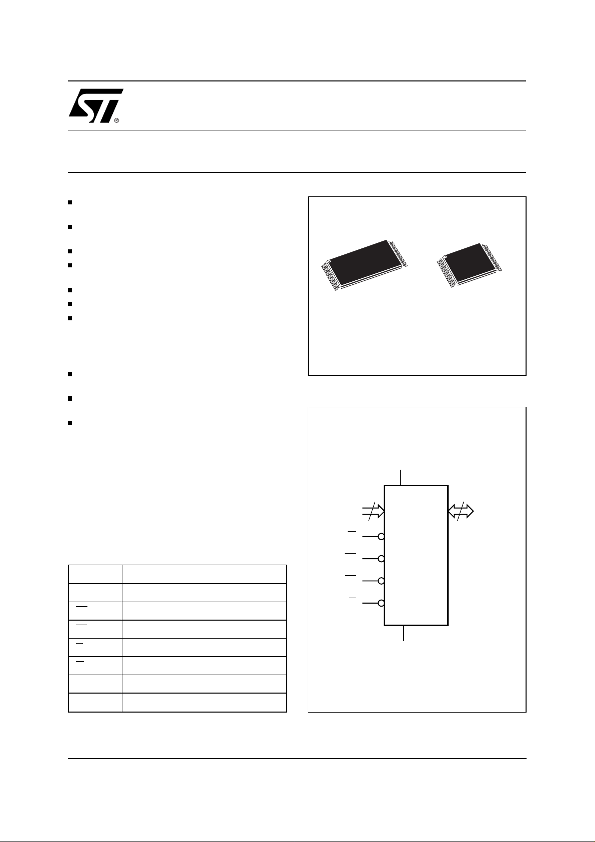
TSOP32 (NA)
8 x 20 mm
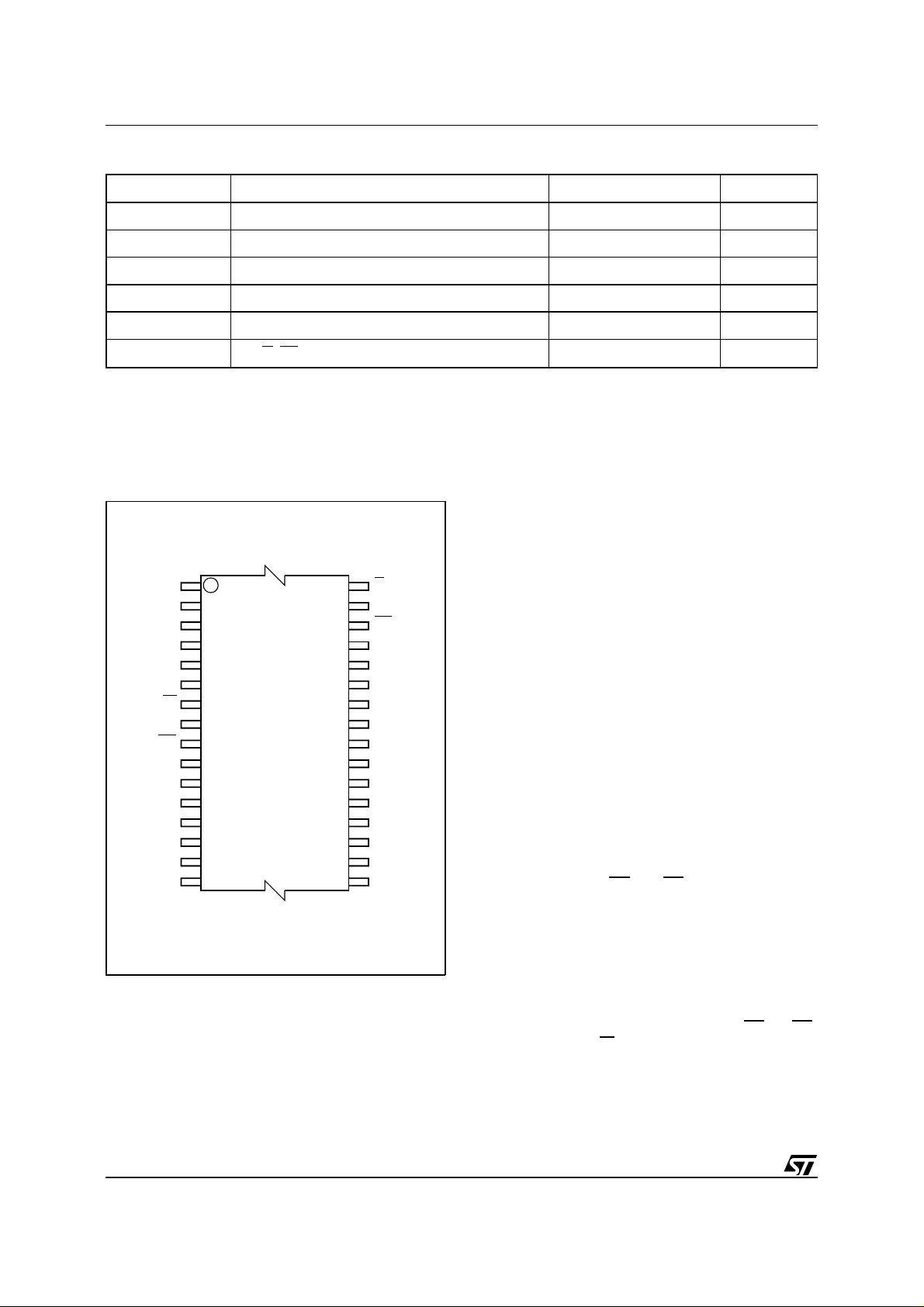
Figure 1. Logic Diagram
TSOP32 (NB)
8 x 14 mm
DESCRIPTION
The M39208 is a memory device combining Flash
and EEPROM into a single chip and using single
supply voltage. The memory is mapped in two
blocks: 2 Mbit of Flash memory and 64 Kbit of
EEPROM memory. Each space is independant for
writing, in concurrent mode the Flash Memory can
be read while the EEPROM is being written.
T ab le 1. Signal Names
A0-A17 Address Inputs
DQ0-DQ7 Data Input / Outputs
EE EEPROM Block Enable
EF Flash Block Enable
G Output Enable
W Write Enable
V
CC
V
SS
Supply Voltage
Ground
A0-A17
W
EE
EF
V
CC
18
M39208
G
V
SS
8
DQ0-DQ7
AI02589
February 1999 1/30
This is preliminary information on a new product now in development or undergoing evaluation. Details are subject to change with out not i ce.
Page 2
M39208
Table 2. Absolute Maximum Ratings
Symbol Parameter Value Unit
T
A
T
BIAS
T
STG
(2)
V
IO
V
CC
, VG, V
V
A9
Notes:
EF
1. Except for the rating "Operating Temperature Range", stresses above those listed in the Table "Absolute Maximum Ratings"
may cause permanent damage to the device. These are stress ratings only and operation of the device at these or any other
conditions above those indicated in the Operating sections of this specification is not implied. Exposure to Absolute Maximum
Rating conditions for extended periods may affect device reliability. Refer also to t he STMicroelectroni cs SURE Pro gr am and other
relevant quality documents.
2. Minimum Voltage may undershoot to –2V during transition and for less than 20ns.
Ambient Operating Temperature –40 to 85
Temperature Under Bias –50 to 125
Storage Temperature –65 to 150
Input or Output Voltages –0.6 to 5 V
Supply Voltage –0.6 to 5 V
(2)
A9, G, EF Voltage –0.6 to 13.5 V
Figure 2. TSOP Pin Connections
(1)
of the data can be secured with the help of the
Software Data Protection (SDP).
The M39208 Flash Memory block offers 4 sectors
of 64 Kbytes, each sector may be erased individually, and programmed Byte-by-Byte. Each sector
A11
A9 A10
A8 EF
A13
A14
A17
V
CC
EE
A16
A15
A12
A7
A6 A1
A5 A2
A4
1
W
8
9
16 17
M39208
32
25
24
AI02587
G
DQ7
DQ6
DQ5
DQ4
DQ3
V
SS
DQ2
DQ1
DQ0
A0
A3
can be separately protected and unprotected
against program and erase. Sector erasure may be
suspended, while data is read from other sectors
of the Flash memory block (or EEPROM memory
block), and then resumed.
During a Program or Erase cycle in the Flash
memory block or during a Write in the EEPROM
memory block, the status of the M39208 internal
logic can be read on the Data Outputs DQ7,DQ6,
DQ5 and DQ3.
PIN DESCRIPTION
Address Inputs (A0-A17).
The address inputs for
the memory array are latched during a write operation. A0-A12 access locations in the EEPROM
memory block A0-A17 access locations in the Flash
memory block. The memory block selected is given
by the state on the
When a specific voltage (V
EE and EF inputs r espectively.
) is applied on the A9
ID
address input, additional specific areas can be
accessed: Read the Manufacturer identifier, Read
the Flash block identifier, Read/Write the EEPROM
block identifier, Verify the Flash Sector Protection
Status.
DESCRIPTION
An additional 64 bytes of EPROM are One Time
Programmable.
The M39208 EEPROM memory block may be written by byte or by page of 64 bytes and the integrity
(Cont’d)
Data Input/Out put (DQ0-DQ7) .
inputs one byte which is latched when
and Write Enable
W are driven active.
Data read is valid when one Chip Enable (Chip
Enable Flash or Chip Enable EEPROM) and Output Enable are driven active. The out put is high
C
°
C
°
C
°
A write operation
EE (or EF)
2/30
Page 3
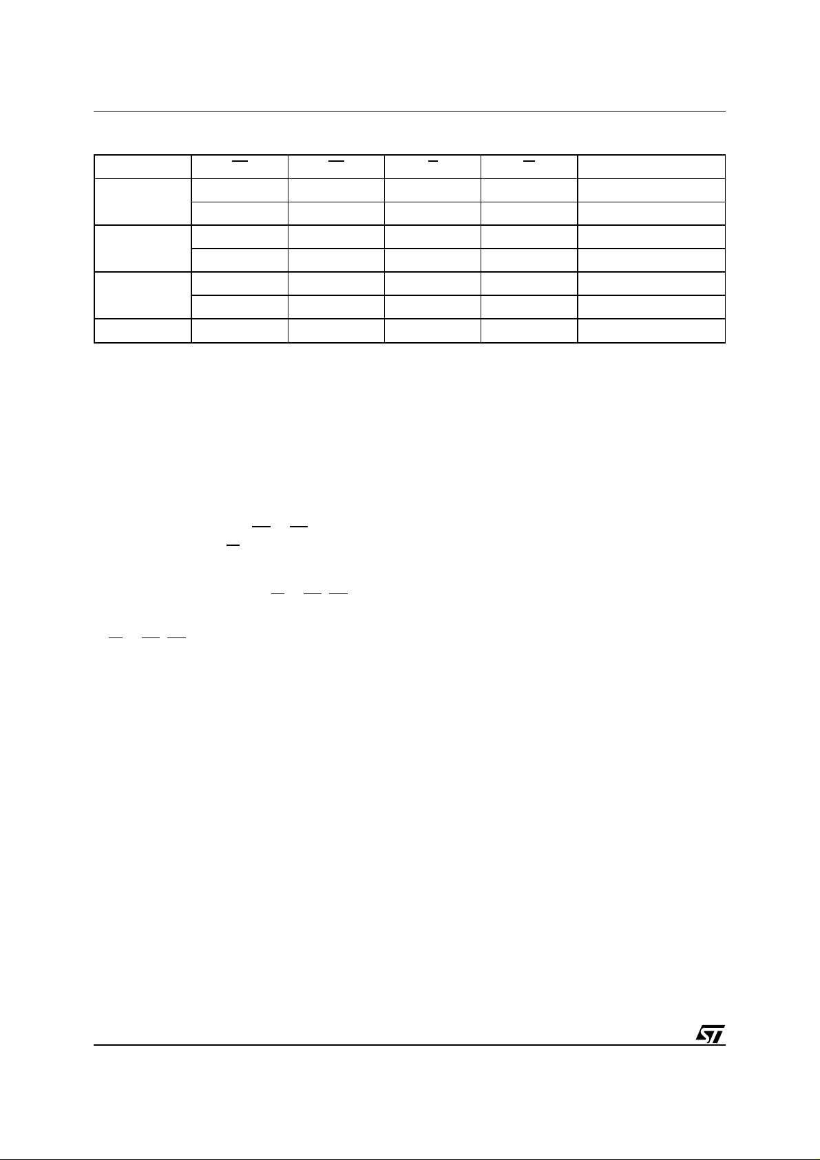
Figure 3. Flash Block Sectors
M39208
A17
AI02588
impedance when the chip is deselected (both
EF driven high) or the outputs are disabled (G
and
A16
1
1
0
0
1
0
1
0
64K Bytes Block
64K Bytes Block
EE
driven high).
Read operations are used to output the contents
from the memory, the Manufacturer identifier, the
Flash Sector protection Status, the Flash block
Identifier, the EEPROM identifier or the OTP row
content.
Memory Block Enable (
Block Enable (
EE or EF) activates the memory
EE and EF).
The Memo ry
control logic, input buffers, decoders and sense
amplifiers. When the
EE input is driven high, the
EEPROM memory block is not selected; when the
EF input is driven high, the Flash memory block is
not selected. Attempts to access both EEPROM
and Flash blocks (
EE low and EF low) are forbidden. Switching between the two memory block
enables (
same clock cycle, a delay of greater than t
EE and EF) must not be made on the
must
EHFL
be inserted.
The M39208 is in standby when both
EF and EE
are High (when no internal Erase or programming
is running). The power consumption is reduced to
the standby level and the outputs are in the high
impedance state, independent of the Output En-
G or Write Enable W inputs.
able
After 150ns of inactivity and when the addresses
are driven at CMOS levels, the chip automatically
enters a pseudo standby mode where consumption
is reduced to the CMOS standby value, while the
outputs continue to drive the bus.
The Output Enable gates the
Output Enable (
G).
outputs through the data buffers during a read
operation. The data outputs are in the high impedance state when the Output Enable
G is High.
TOP
ADDRESS
3FFFFh
2FFFFh
1FFFFh
0FFFFh
BOTTOM
ADDRESS
30000h
20000h
10000h
00000h
During Sector Protect and Sector Unprotect operations, the
G input must be forced to VID level (12V
+ 0.5V) (for Flash memory block only).
Addresses are latched on the
Write Enable (
falling edge of
the rising edge of
W).
W, and Data Inputs are latched on
W.
OPERATIONS
The M39208 memory is addressed through 18
inputs A0-A17 and provides data on eight Data
Inputs/Outputs DQ0-DQ7 with the help of four control lines: Chip Enable EEPROM (
Flash (
(
EF), Output Enable (E) and Write Enable
W) inputs.
EE), Chip Enable
An operation is defined as the basic decoding of
the logic level applied to the control input pins (
EF,
EE, G, W) and the specified voltages applied on
the relevant address pins. These operat ions are
detailed in Table 3.
Read.
is
Both Chip Enable and Output Enable (that
EF and G or EE and G) must be low in order to
read the output of the memory.
Read operations are used to output the contents
from the Flash or EEPROM block , the Manufacturer identifier, the Flash Sector protection Status,
the Flash block Identifier, the EEPROM identifier or
the OTP row content.
Notes:
– The Chip Enable input mainly provides power
control and should be used for device selection.
The Output Enable input should be used to gate
data onto the output in combination with active
EF or EE input signals.
– The data read depends on the previous instruc-
tion entered into the memory (see Table 4).
3/30
Page 4
M39208
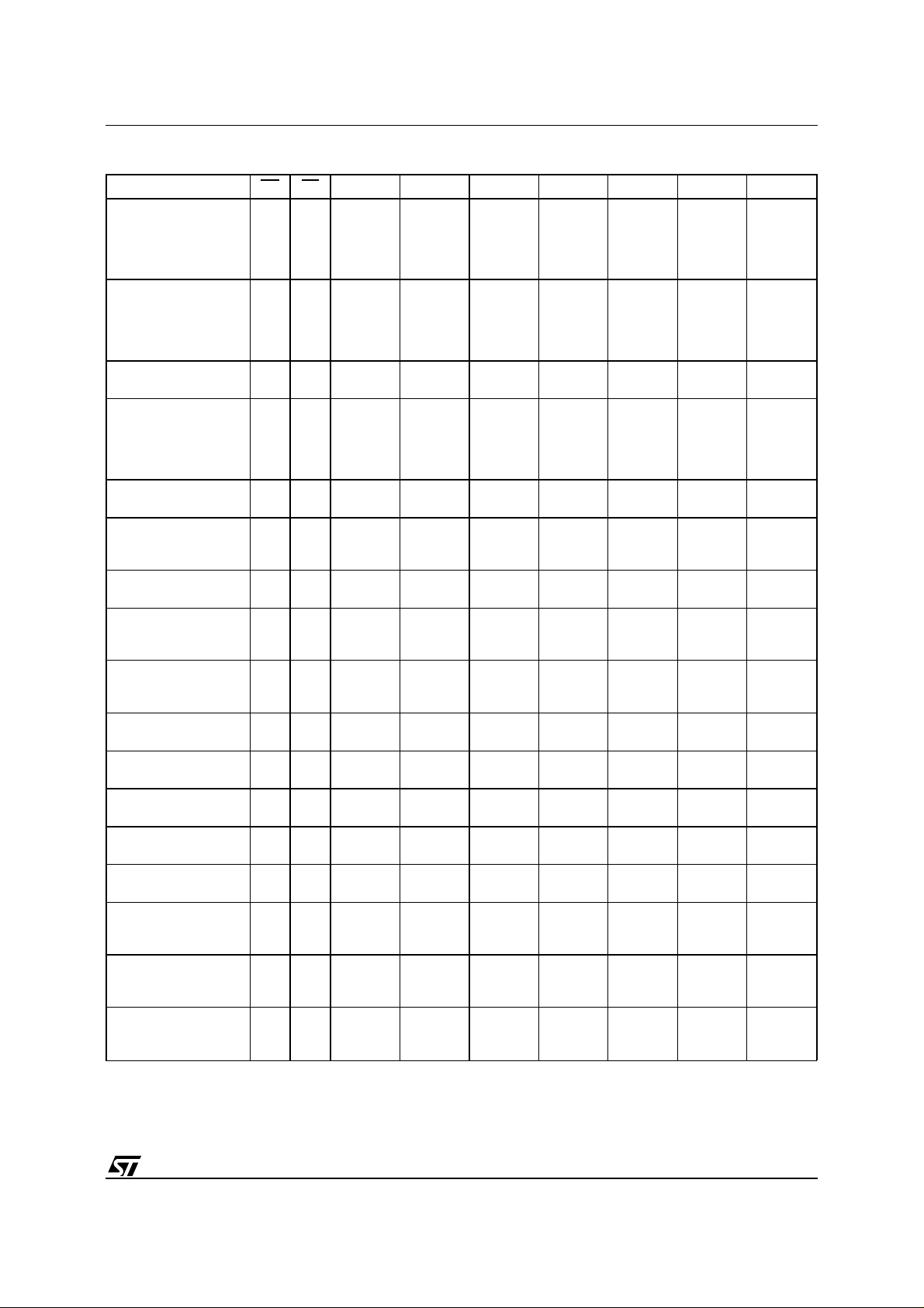
Table 3. Basic Operations
Operation EF EE G W DQ0 - DQ7
V
Read
Write
Output Disable
Standby V
Note:
X = V
or VIH.
IL
A W rite operation can be used for two goals:
Write.
IL
V
IH
V
IL
V
IH
V
IL
V
IH
IH
V
IH
V
IL
V
IH
V
IL
V
IH
V
IL
V
IH
– either write data in the EEPROM memory block
– or enter a sequence of bytes composing an
instruction.
The reader should note that Programming a Flash
byte is an instruction (see Instructions paragraph).
Writing data requires:
– the Chip Enable (either
– the Write Enable (
EE or EF) to be Low
W) to be Low with Output
Enable (G) High.
Addresses in Flash block (or EEPROM block) are
latched on the falling edge of
W or EF (EE) whichever occurs last; the data to be written in Flash
block (EEPROM block) is latched on the rising edge
W or EF (EE) whichever occurs first.
of
Specific Read and Write Operations.
Device
specific data is accessed through operations decoding the V
level applied on A9 ( VID = 12V +
ID
0.5V) and the logic levels applied on address inputs
(A0, A1, A6). These specific operations are:
– Read the Manufacturer identifier
– Read the Device identifier
– Define the Flash Sector protection
– Read the EEPROM identifier
– Write the EEPROM identifier
Note: The OTP row (64 bytes) is acc es sed with a
specific software sequence detailed in the paragraph "Write in OTP row".
Instructions
An instruction is defined as a sequence of specific
Write operations. Each received byte is sequentially decoded (and not executed as standard Write
operations) and the instruction is executed when
V
IL
V
IL
V
IH
V
IH
V
IH
V
IH
XX Hi-Z
V
IH
V
IH
V
IL
V
IL
XHi-Z
XHi-Z
Read in Flash Block
Read in EEPROM Block
Write in Flash Block
Write in EEPROM Block
the correct number of bytes are properly received
and the time between two consecutive bytes is
shorter than the time-out value.
The sequencing of any instruction must be followed
exactly , any invalid combination of instruction bytes
or time-out between two consecutive bytes will
reset the device logic into a Read memory state
(when addressing the Flash block) or directly decoded as a single operation when addressing the
EEPROM block.
The M39208 set of instructions includes:
– Program a byte in the Flash block
– Read a Flash sector protection status
– Erase instructions: Flash Sector Erase, Flash
Block Erase, Flash Sector Erase Suspend, Flash
Sector Erase Resume
– EEPROM power down
– Deep power down
– Set/Reset the EEPROM software writ e protec-
tion (SDP)
– OTP row access
– Reset and Return
– Read identifiers: read the manufacturer identi-
fier, Read the Flash block identifier
These instructions are detailed in Table 4.
For efficient decoding of the instruction, the two first
bytes of an instruction are the coded cycles and are
followed by a command byte or a confirmation byte.
The coded cycles consist of writing the data AAh at
address 5555h during the first cycle and data 55h
at address 2AAAh during the second cycle.
In the specific case of the Erase instruction, the
instruction expects confirmation by two additional
coded cycles.
4/30
Page 5
M39208
T able 4. Instructions
(1)
Instruction EE EF Cycle 1 Cycle 2 Cycle 3 Cycle 4 Cycle 5 Cycle 6 Cycle 7
Read
Read Manufacturer
Identifier
(2)
10
AAh
@5555h
55h
@2AAAh
90h
@5555h
Identifier
with
(A0,A1,A6)
at (0,0,0)
Read
Read Flash
Identifier
(2)
10
AAh
@5555h
55h
@2AAAh
90h
@5555h
identifier
with
(A0,A1,A6)
at (1,0,0)
Read OTP Row 0 1
AAh
@5555h
55h
@2AAAh
90h
@5555h
Read
byte 1
Read
byte 2
Read
Read Block
Protection Status
(2)
10
AAh
@5555h
55h
@2AAAh
90h
@5555h
Identifier
with
(A0,A1,A6)
at (0,1,0)
Program a Flash Byte 1 0
Erase one Flash
Block
10
Erase the Whole Flash 1 0
AAh
@5555h
AAh
@5555h
AAh
@5555h
55h
@2AAAh
55h
@2AAAh
55h
@2AAAh
A0h
@5555h
80h
@5555h
80h
@5555h
Data
@address
AAh
@5555h
AAh
@5555h
55h
@2AAAh
55h
@2AAAh
30h
@Sector
address
10h
@5555h
B0h
Suspend Block Erase 1 0
@any
address
30h
Resume Block Erase 1 0
@any
address
EEPROM Power
Down
01
Deep Power Down 1 0
SDP Enable
(EEPROM)
SDP Disable
(EEPROM)
01
01
Write in OTP Row 0 1
Return (from OTP
Read or EEPROM
01
Power Down)
Reset 1 0
Reset (short
instruction)
Notes:
1. AAh @5555h means Write byte AAh at address 5555h.
2. This instruction can also be performed as a simple Read operation with A9=V
3. Additional blocks to be erased must be entered within 80µs.
10
AAh
@5555h
20h
@5555h
AAh
@5555h
AAh
@5555h
AAh
@5555h
F0h @
any
address
AAh
@5555h
F0h
@any
address
55h
@2AAAh
55h
@2AAAh
55h
@2AAAh
55h
@2AAAh
55h
@2AAAh
30h
@5555h
A0h
@5555h
80h
@5555h
B0h
@5555h
F0h
@any
Address
Write
byte 1
AAh
@5555h
Write
byte 1
(refer to READ chapter).
ID
Write
byte 2
55h
@2AAAh
Write
byte 2
20h
@5555h
Read
byte N
30h
@Sector
address
Write
byte N
Write
byte N
(3)
5/30
Page 6
M39208
T ab le 5. Device Identifiers
Identifier EF EE G WA0A1A6A9
Read the
Manufacturer
Identifier
Read the Flash
Block Identifier
Read the
EEPROM Block
Identifier
Note:
X = Don’t Care.
POWER SUPPLY and CURRENT CONSUMPTION
EEPROM Power Down.
with the EEPROM in power down with the help of
the EEPROM power down instruction (see Table
4). Once the EEPROM power down instruction is
decoded, the EEPROM block cannot be ac ces sed
unless a further Return instruction is decoded.
Deep Power Down.
lowest I
consumption mode with the help of the
CC
Deep Power Down instruction (see Table 4). Once
the instruction is d ecoded, the device is set in a
sleep mode until a Reset instruction is decoded.
Power Up.
The M39208 internal logic is reset upon
a power-up condition to Read memory status. Any
Write operation in EEPROM is inhibited during the
first 5 ms following the power-up.
Either
EF, EE or W must be tied to VIH during
Power-up for the maximum security of the data
contents and to remove the possibility of a byte
being written on the first rising edge of
W. Any write cycle initiation is locked when Vcc is
below V
LKO
.
READ
Read operations and instructions can be used to:
– read the contents of the Memory Array (Flash
block and EEPROM block)
– read the Memory Array (Flash block and
V
V
V
V
IL
V
IL
V
IH
V
IH
V
IH
V
IL
V
IL
IL
IL
IH
V
IH
V
IH
The M39208 can be set
The M39208 can be set in the
EF, EE o r
V
V
V
IL
V
IH
XXVILV
V
IL
IL
IL
V
IL
Read data (Flash a nd EEPR OM bloc ks)
Both Chip Enable
G) must be low in order to read the data from the
(
memory.
Read the Manufacturer Identifier
The manufacturer’s identifier can be read with two
methods: a Read operation or a Read instruction.
Read Operation.
be read with a Read operation with specific logic
levels applied on A0, A1, A6 and the V
= 12V + 0.5V) on A9 (see Table 5).
Read Instruction.
can also be read with a single instruction composed
of 4 operations: 3 specific Write operations (see
Table 4) and a Read which outputs the Manufacturer identifier, the Flash block identifier or the Flash
sector protection status.
Read the Flash Block Identifier
The Flash block identifier can be read with two
methods: a Read operation or a Read instruction.
Read Operation.
can be read with a single Read operation with
specific logic levels applied on A0, A1, A6 and the
level on A9 (see Table 5).
V
ID
Read Instruct ion.
also be read with an instruction composed of 4
operations: 3 specific Write operations and a Read
(see Table 4).
EEPROM block) status and identifiers.
Other
Addresses
V
ID
V
ID
ID
Don’t Care 20h
Don’t Care t.b.d.
Don’t Care
DQ0 - DQ7
64 bytes
user
defined
EF (or EE) and Output Enable
The manufacturer’s identifier can
level (V
ID
The manufacturer’s identifier
The Flash block identifier (t.b.d.)
The Flash block identifier can
ID
6/30
Page 7

T able 6. Status Bit
EF EE DQ7 DQ6 DQ5 DQ4 DQ3 DQ2 DQ1 DQ0
M39208
Flash V
EEPROM V
Note:
X = Not guaranteed value, can be read either ’1’ or ’0’.
V
IL
V
IH
Data
IH
Polling
Data
IL
Polling
Toggle
Flag
Toggle
Flag
Read the EEPROM Block Identifier
The EEPROM block identifier (64 bytes, user defined) can be read with a single Read operation with
A6 = ’0’ and A9 = V
(see Table 5).
ID
Read the OTP Row
The OTP row is mapped in the EEPROM block
EE = ’0’, EF = ’1’). Read of the OTP row (64 bytes)
(
is by an instruction (see T able 4) composed of three
specific Write operations of data bytes at three
specific memory locations (each location in a different page) before reading the OTP row content.
When accessing the OTP row, only the LSB addresses (A6 to A0) are dec oded where A6 mus t be
’0’.
Each Read of the OTP row has to be followed by
the Return instruction (see Table 4).
Read the Flash Sector Protection Status
Reading the Flash sector protection status is by an
instruction similar to the Read Manufacturer identifier instruction, the only difference being the value
of the logic levels applied on A0, A1, A 6, while A16
and A17 define the Flash sector whose protection
has to be verified. Such a read instruction will
output a 01h if the Flash sector is protected and a
00h if the Flash sector is not protected.
The Flash sector protection status can also be
verified with a Read operation (see chapter: Flash
block specific features), with V
on A9.
ID
Read the Status Bits
The M39208 provides several Write operation
status flags which may be used to minimize the
application write (or erase or program) time. These
signals are available on the I/O port bits when
programming (or erasing) are in progress.
Data Polling flag, DQ7.
When Erasing or Programming into the Flash block (or when Writing into
the EEPROM block), bit DQ7 outputs the complement of the bit being entered for Programming/Writing on DQ7. Once the Program
instruction or the Write operation is per formed, the
Error
Flag
XXXXXX
X
Erase
Time-out
XXX
true logic value is read on DQ7 (in a Read operation).
Flash memory block specific features:
– Data Polling is effective after the fourth W pulse
(for programming) or after the sixth W pulse (for
Erase). It must be performed at the address
being programmed or at an address within the
Flash sector being erased.
– During an Erase instruction, DQ7 outputs a ’0’.
After completion of the instruction, DQ7 will output the last bit programmed (that is a ’1’ after
erasing).
– if the byte to be programmed is in a protected
Flash sector, the instruction is ignored.
– If all the Flash sectors to be erased are pro-
tected, DQ7 will be set to ’0’ for about 100µs, and
then return to t he previous addressed byte. No
erasure will be performed.
– if all sectors are protected, a Bulk Erase instruc-
tion is ignored.
T oggle flag, DQ6.
The M39208 also offers another
way for determining when the EEPROM write or
the Flash memory Program instruction is completed. During the internal Write operation, the DQ6
will toggle from ’0’ to ’1’ and ’1’ to ’0’ on subsequent
attempts to read any byte of the memory, when
G , EE or EF is low.
either
When the internal cycle is completed the toggling
will stop and the data read on DQ0-DQ7 is the
addressed memory byte. The device is now accessible for a new Read or Write operation. The operation is completed when two successive reads yield
the same output data.
Flash memory block specific features:
a. the T oggle bit is effective after the fourth
(for programming) or after the sixth
W pulse
W pulse (for
Erase).
b. If the byte to be programmed belongs to a pro-
tected Flash sector, the instruction is ignored and:
7/30
Page 8
M39208
Figure 4. EEPROM SDP Enable Flowcharts
Page
Write
Instruction
WRITE AAh in
Address 5555h
WRITE 55h in
Address 2AAAh
WRITE A0h in
Address 5555h
SDP is set
SDP ENABLE ALGORITHM
Page
Write
Instruction
SDP
Set
WRITE AAh in
Address 5555h
WRITE 55h in
Address 2AAAh
WRITE A0h in
Address 5555h
WRITE Data to
be Written in
any Address
Write
in Memory
SDP
not Set
WRITE
is enabled
Write Data
+
SDP Set
after tWC
AI01698B
– if all the Flash sectors selected for erasure
are protected, DQ6 will toggle to ’0’ for about
100µs, and then return to the previous addressed byte.
– if all sectors are protected, the Bulk Erase in-
struction is ignored.
Error flag, DQ5 (F lash block only).
This bit is set
to ’1’ when there is a failure during either a Flash
byte programming or a Sector erase or the Bulk
Erase.
In case of error in Flash sector erase or byte
program, the Flash sector in which the error occurred or to which the programmed byte belongs,
must not be used any longer (other Flash sectors
may still be used). The Error bit resets after Reset
instruction.
During a correct Program or Erase, the Error bit will
set to ’0’.
Erase Time-out flag, DQ3 (Flash block only).
The Erase Timer bit reflects the time-out period
allowed between two consecutive Sector Erase
instructions. The Erase timer bit is set to ’0’ after a
Sector Erase instruction for a time period of 100µs
20% unless an additional Sector Erase instruction
±
is decoded. After this time period or when the
additional Sector Erase instruction is decoded,
DQ3 is set to ’1’.
WRITE a BYTE (or a P AGE ) in EEPROM
It should be noticed that writing in the EEPROM
block is an operation, it is not an instruction (as for
Programming a byte in the Flash block).
Write a Byte in EEPROM Block
A write operation is initiated w hen Chip Enable
is Low and Write Enable
Enable
edge of
G High. Addresses are latched on the falling
W, EE whichever occurs last.
W is Low with Output
EE
Once initiated, the write operation is internally
timed until completion, that is during a time t
.
W
The status of the write operation can be found by
reading the Data Polling and Toggle bits (as detailed in the READ chapter) or the Ready/Busy
output. This Ready/Busy output is driven low from
the write of the byte being written until the completion of the internal Write sequence.
8/30
Page 9
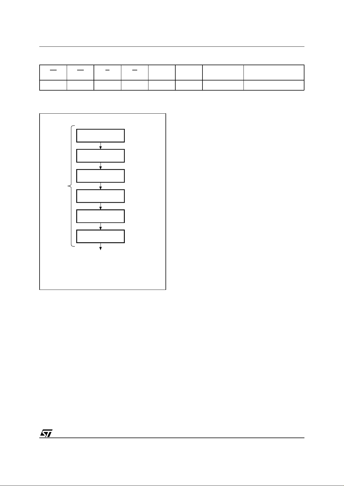
T ab le 7. Write the EEPROM Block Identifier
M39208
EF EE G WA6A9
V
IH
Figure 5. SDP disable Flowchart
V
IL
V
IH
V
IL
V
IL
V
period (between two consecutive Write operations)
that is smaller than the t
time exceeds the t
ming cycle will start.
WRITE AAh in
Address 5555h
EEPROM Block Software Data Protection
A protection instruction allows the user to inhibit all
WRITE 55h in
Address 2AAAh
write modes to the EEPROM block: the Software
Data Protection (referenced as SDP in the following). The SDP feature is useful for protecting the
EEPROM memory from inadvertent write cycles
Page
Write
Instruction
WRITE 80h in
Address 5555h
WRITE AAh in
Address 5555h
that may occur during uncontrolled bus conditions.
The M39208 is shipped as standard in the unpro-
tected state meaning that the EEPROM memory
contents can be changed by the user. After the SDP
enable instruction, the device enters the Protect
Mode where no further write oper ations have any
WRITE 55h in
Address 2AAAh
effect on the EEPROM memory contents.
The device remains in this mode until a valid SDP
disable instruction is received whereby t he device
WRITE 20h in
Address 5555h
Unprotected State
after
tWC (Write Cycle time)
AI01699B
reverts to the unprotected state.
T o enable the Software D ata Protection, the device
has to be written (with a Page Write) with three
specific data bytes at three specific memory locations (each location in a different page) as shown
in Figure 4. This sequence provides an unlock key
to enable the writ e action, and, at t he same time,
SDP continues to be set. Any further Write in
EEPROM when the SDP is set will use this same
sequence of three specific data bytes at three
Write a Page in EEPROM Block
The Page write allows up to 64 bytes within the
same EEPROM page to be consecutively latched
into the memory prior t o initiating a programming
cycle. All bytes must be located in a single pa ge
address, that is A6-A12 must be the same for all
bytes. Once initiated, the Page write operation is
internally timed until completion, that is during a
WC
.
time t
The status of the write operation can be seen by
reading the Data Polling and Toggle bits (as detailed in the READ chapter).
A Page write is composed of successive Write
instructions which must be sequenced within a time
specific memory locations followed by the bytes to
write. The first SDP enable sequence can be directly followed by the bytes to written.
Similarly, to disable the Software Data Protection
the user has to write specific data bytes into six
different locations with a Page Write addressing
different bytes in different pages, as shown in Figure 5.
The Software Data Protection state is non-volatile
and is not changed by power on/off sequences. The
SDP enable/disable instructions set/reset an internal non-volatile bit and therefore will require a write
time t
only on the Toggle bit (status bit DQ6).
Other
Addresses
ID
WC
Don’t Care 64 bytes User Defined
WLWL
value, the internal program-
WLWL
, This Write operation can be m onitored
DQ0 - DQ7
value. If this period of
9/30
Page 10

M39208
Figure 6. Data Polling Flowchart
START
READ DQ5 & DQ7
at VALID ADDRESS
DQ7
YES
=
DATA
NO
NO
DQ5
= 1
YES
READ DQ7
DQ7
YES
=
DATA
NO
FAIL PASS
Figure 7. Data Toggle Flowchart
START
READ
DQ5 & DQ6
DQ6
=
TOGGLE
NO
DQ5
= 1
READ DQ6
DQ6
=
TOGGLE
FAIL PASS
NO
YES
YES
NO
YES
AI01369
Write OTP Row
Writing (only one time) in the OTP row (64 bytes)
is enabled by an instruction. This instruction is
composed of three specific Write operations of data
bytes at three specific memory locations (each
location in a different page) followed by the the data
to store in the OTP row (refer to Table 4).
When accessing the OTP row, the only LSB addresses (A6 to A0) are decoded, with A6 = ’0’.
Write the EEPROM Block Identifier
The EEPROM block identifier can be written with a
single Write operation with specific logic levels
applied on A6 and the V
level on A9 (see Tab le
ID
7).
PROGRAM in the Flash BLOCK
It should be noted that writing data into the
EEPROM block and the Flash block is not per-
AI01370
formed in a similar way: the Flash memory requires
an instruction (see Instruction chapter) for Erasing
and another instruction for Programming one (or
more) byte(s), the EEPROM memory is directly
written with a simple operation (see Operation
chapter).
Program Instuction.
During the execution of the
Program instruction, the Flash block memory will
not accept any further instructions.
The Flash block memory can be program med byteby-byte. The program instruction is a sequence of
three specific Write operations followed by writing
the address and data byte to be programmed into
the Flash block memory (see T able 4). The M39208
automatically starts and performs the programming
after the fourth write operation.
During programming, the memory status may be
checked by reading the status bits DQ5, DQ6 and
DQ7, as detailed in the following sections.
10/30
Page 11

M39208
Data Polling.
Polling on DQ7 is a method of checking whether a Program or an Erase ins truction is in
progress or completed (see Figure 6). When a
Program instruction is in progress, data bit DQ7 is
the complement of the original data bit 7; when
DQ7 is identical to the old data and the Error bit
DQ5 is still ’0’, the instruction is complete. To determine if DQ7 is valid, each poll must store the
original data for comparison, and if t hey are the
same, it can be considered that the operation was
successful. The Error bit DQ5 is checked to ensure
timing limits have not exceeded.
When an Erase operation is in progress, DQ7 is
always ’0’, and will be ’1’ when finished, so long as
DQ5= ’0’.
In all cases, when DQ5 is ’1’, DQ7 should be
checked again, in case DQ7 changed simultaneously with DQ5. If DQ7 = true dat a (Program) or
DQ7 = ’1’ (Erase), the operation is successful and
execution should return to the caller. A suggested
second read will provide all true data (Program) or
all FFh (Erase). Otherwise, this should be flagged
as an error, and the device should be Reset.
Data Toggle.
Checking the Toggle bit DQ6 is an
alternative method of checking if Program or Erase
operations are in progress or com pleted (see Figure 7). When an operation is in progress, data bit
DQ6 constantly toggles for successive read operations. When DQ6 no longer toggles and t he Error
bit DQ5 is ’0’, the operation is com pleted. To determine if DQ6 has toggled, each polling action requires 2 consecutive read operations of the data,
and if the data read is the same, it can be considered that the operation was successful. The Error
bit DQ5 is checked to ensure timing limits hav e not
been exceeded. In all cases, when DQ5 is ’1’, DQ6
should be checked again, in case DQ6 has
changed simultaneously with DQ5. If DQ6 has
stopped toggling, the o peration is successful and
execution should return to the caller. A suggested
second read will provide all true data (Program) or
all FFh (Erase). Otherwise, this event should be
flagged as an error, and the device should be
Reset.
ERASE in the Flash BLOCK
It should be noted that:
a. Programming any byte of one Flash sector (or
bulk) requires that the Flash sector (or bulk) has
been previously erased (once for all bytes within
the sector or bulk) with the correct instruction (see
Instructions chapter).
b. Writing in the EEPROM memory is an operation
triggering an automatic sequencing of byte erase
followed by a byte write. Writing in EEPROM does
not require a specific erase operation before writing.
Bulk Erase Instruction.
The Bulk Erase instruction uses six write operations followed by Read
operations of the status register bits, as desc ribed
in Table 4. If any byte of the Bulk Erase instruction
is wrong, the Bulk Erase instruction aborts and the
device is reset to the Read Flash memory status.
During a Bulk Erase, the memory status may
checked by reading the status bits DQ5, DQ6 and
DQ7, as detailed in the "PROGRAM in t he Flash
BLOCK" chapter. The Error bit (DQ5) returns a ’1’
if there has been an Erase Failure (maximum number of erase cycles have been executed).
It is not necessary to program the array with 00h,
the M39208 will automatically do this before erasing to FFh.
During the execution of the Bulk Erase instruction,
the Flash block logic does not accept any instruction.
Sector Erase in Flash Block.
The Sector Erase
instruction uses six write operations, as described
in Table 4. Additional Flash Sector Erase confirm
commands and Flash sector addresses can written
subsequently to erase other Flash sectors in parallel, without further coded cycles, if the additional
instruction is transmited in a shorter time than the
timeout period to end of period. The input of a new
Sector Erase instruction will restart the time-out
period.
The status of the internal timer can be monitored
through the level of DQ3 (Erase time-out bit), if DQ3
is ’0’ the Sector Erase instruction has been received and the timeout is counting; if DQ3 is ’1’, the
timeout has expired and the M39208 is erasing the
Flash sector(s). Before and during Erase timeout,
any instruction different than Erase suspend and
Erase Resume will abort the instruction and reset
the device to read array mode.
It is not necessary to program the Flash sector with
00h as the M39208 will do this automatically before
erasing (byte = FFh).
During a Sector Erase, the memory status may be
checked by reading the status bits DQ5, DQ6 and
DQ7, as detailed in the "Program instruction" chapter. During the execution of the erase instruction,
the Flash block logic accepts only the Reset and
Erase Suspend instructions (erasure of one Flash
sector may be suspended, in order to read data
from another Flash sector, and then resumed).
11/30
Page 12

M39208
T ab le 8. Flash Sector Protection
EF EE G W A0 A1 A6 A9 A12 A16 A17 DQ0 - DQ7
V
V
Notes:
V
IL
V
IL
X = Don’t care.
SA = Software Address.
V
IH
IH
ID
V
IL
V
V
XXXVIDX SA SA Prot ection Activation
IL
V
IH
V
IL
V
IH
V
IL
XSASA
ID
Verify the protection status:
when DQ0= 1, the sector is
protected
T able 9. Flash Unprotection
EF EE G W A0 A1 A6 A9 A12 A15 A16 A17 DQ0 - DQ7
V
V
V
ID
IH
V
V
IL
IH
Notes:
X = Don’t care.
SA = Software Address.
V
ID
V
V
IL
Erase Suspend Instruction.
XXXVIDV
IL
V
V
IH
IL
V
IH
When a Flash Sector
V
IH
Erase operation is in progress, the Erase Suspend
instruction may suspend the operation by writing
V
IH
X X SA SA
ID
IH
XX
eration may be resumed by this instruction. The
Erase Resume instruction consists of writing 30h
at any address (see Table 4).
Activation of Unprotected
Mode
Verify the protection status:
when 00h, the sector is
unprotected
B0h at any address (see Table 4). This allows
reading of data from another Flash sector while
erase is in progress. Erase suspend is accepted
only during the Flash Sector Eras e instruction execution and defaults to read array mode. An Erase
Suspend instruction entered during an Erase
timeout will, in addition to suspending the erase,
terminates the timeout.
The Toggle bit DQ6 stops toggling when the
M39208 internal logic is suspended. The Toggle bit
status must be monitored at an address out of the
Flash sector being erased. Toggle bit will stop
toggling between 0.1µs and 15µs after the Erase
Suspend instruction has been written. The M39208
will then automatically be set into Read Flash Block
Memory Array mode.
When erase is suspended, Reading from Flash
sectors being erased will output invalid data, a
Read from Flash sector not being erased is valid.
During an Erase Suspend, the Flash memory will
respond only to Erase Resume and Reset instructions.
A Reset instruction will definitively abort erasure
and can leave invalid data in the Flash sectors
being erased.
Erase Resume Instruction.
If an Erase Suspend
instruction was previously executed, the erase op-
FLASH BLOCK SPECIFIC FEATURES
Flash Sector Pro tection.
Each Flash sector can
be separately protected against Program or Erase.
Flash Sector Protection provides additional data
security , as it disables all program or erase operations. This mode is activated when both A9 and
are set to V
(12V + 0.5V) and the Flash sector
ID
address is applied on A16 and A17, as shown in
Figure 8 and T able 8.
Flash sector protection is programmed with the
help of a specific sequence of levels applied on
EE, G, A0, A1, A6, A9, A16 and A17; this sequence
includes a verification of the Protection status on
DQ0 as shown in Table 8.
Any attempt to program or erase a pr otected Flash
sector will be ignored by the device.
Remarks:
– The Verify operation is a read with a simulated
worst case conditions. This allows a guarantee
of the retention of the Protection status
– During the application life, the Sector pr otection
status can be accessed with a regular Read
instruction without applying a "high voltage" V
on A9. This instruction is detailed in T able 4.
G
EF,
ID
12/30
Page 13

Figure 8. Sector Protection Flowchart
SECTOR ADDRESS
START
on A16, A17
EE = V
IH
n = 0
G, A9 = VID,
EF = V
IL
Wait 4µs
W = V
IL
Wait 100µs
M39208
W = V
IH
G = V
IH
Wait 4µs
READ DQ0 at PROTECTION
ADDRESS: A0, A6 = VIL, A1 = VIH and
A16, A17 DEFINING SECTOR
DQ0
A9 = V
PASS
NO
= 1
YES
IH
++n
= 25
A9 = V
FAIL
NO
YES
IH
AI02598
13/30
Page 14

M39208
Figure 9. Sector Unprotecting Flowchart
START
EE = EF = V
n = 0
A6, A12, A15 = V
G, A9 = V
EF, G, A9 = V
Wait 10ms
EF, G = V
Wait 4µs
Wait 4µs
W = V
W = V
Wait 4µs
IH
IL
IH
IH
IH
IH
ID
Note:
14/30
NO LAST
1. A6 is kept at V
reads, A6 must be kept at V
during unprotection algorithm in order to secure best unprotection verification. During all other protection status
IH
++n
= 1000
YES
FAIL
IL
READ at UNPROTECTION
ADDRESS: A1, A6 = VIH, A0 = V
A16, A17 DEFINING SECTOR
(see Note 1)
DATA
=
00h
and
IL
YESNO
INCREMENT
SECTOR
NO
SECT.
YES
PASS
AI02597
.
Page 15

M39208
T able 10. AC Measurement Conditions
Input Rise and Fall Times
Input Pulse Voltages 0.45V to 2.4V
Input Timing Ref. Voltages 0.8V and 2V
Output Timing Ref. Voltages 1.5V
10ns
≤
Figure 10. AC Testing Input Out put Waveform
2.4V
1.5V
0.45V
AI01950
(1)
T ab le 11. Capacitance
Symbol Parameter Test Condition Min Max Unit
C
IN
C
OUT
Note:
1. Sampled only, not 100% tested.
Input Capacitance VIN = 0V 6 pF
Output Capacitance V
(TA = 25 °C, f = 1 MHz )
Figure 11. Output AC Testing Load Circuit
V
CC
I
OL
DEVICE
UNDER
TEST
I
OH
CL includes JIG capacitance
V
= 1.5V when the DEVICE
OUT
UNDER TEST is in the
Hi-Z output state.
= 0V 12 pF
OUT
CL = 30pF
AI02596B
Flash Sector Unprotection.
Flash sectors can be
unprotected to allow updating of their contents.
Note that the Sector Unprotection unprotects all
sectors (sector 0 up to sector 7).
Flash Sector Unprotection is activated with a specific sequence of levels applied on
EF, EE, G, A 0,
A1, A6, A9, A12 and A15; this sequence includes a
verification of the Protection status on DQ0-DQ7
as shown in Figure 9 and Table 9.
This allows a guarantee of the retention of the
Protection status.
Remarks:
– The Verify operation is a read with a simulated
worst case conditions. This allows a guarantee
of the retention of the Protection status
– During the application life, the Sector pr otection
status can be accessed with a regular Read
instruction without "high voltage" V
on A9. This
ID
instruction is detailed in Table 4.
Reset Instruction.
The Reset instruction resets
the device internal logic in a f ew µs. Reset is an
instruction of either one write operation or three
write operations (refer to Table 4).
Supply Rails .
Normal precautions must be taken
for supply voltage decoupling, each device in a
system should have the V
0.1µF capacitor close to the V
rail decoupled with a
CC
and VSS pins. The
CC
printed circuit board trace width should be suff icient
to carry the V
program and erase currents re-
CC
quired.
15/30
Page 16

M39208
T ab le 12. DC Characteristics
(T
= 0 to 70°C or –20 to 85°C or –40 to 85°C; VCC = 2.7 V to 3.6V)
A
Symbol Parameter Test Condition Min Max Unit
I
Note:
I
I
CC1
I
CC2
I
CC3
I
CC4
I
CC5
I
CC6
V
V
V
V
V
I
V
LKO
LO
ID
Input Leakage Current 0V ≤ VIN ≤ V
LI
Output Leakage Current 0V ≤ V
(1)
Supply Current (Read Flash) TTL
Supply Current (Read EEPROM)
TTL
EE = VIH, EF = VIL, G =
V
, f = 6MHz
IH
EE = VIL, EF = VIH, G =
V
, f = 6MHz
IH
OUT
≤ V
CC
CC
Supply Current (Standby) CMOS EF = EE = VCC ± 0.2V 60
Supply Current (Flash Block
Program or Erase)
Supply Current (EEPROM Write) During t
Supply Current in Deep Power
Down Mode
Input Low Voltage –0.5 0.8 V
IL
Input High Voltage 0.7 V
IH
Output Low Voltage IOL = 1.8mA 0.45 V
OL
Output High Voltage IOH = –100µAV
OH
A9 High Voltage 11.5 12.5 V
ID
VID Current A9 = V
Byte program, Sector or
Chip Erase in progress
WC
After a Deep Power Down
instruction (see Table 4)
ID
VCC Minimum for Write, Erase and
Program
1. When reading the Flash block when an EEPROM byte(s) is under a write cycl e, the supply cur rent is I
1
±
1
±
15 mA
15 mA
20 mA
20 mA
2
CC
–0.4 V
CC
VCC + 0.3 V
100
2 2.3 V
+ I
CC5
.
CC1
A
µ
A
µ
A
µ
A
µ
A
µ
GLOSSARY
Block:
EEPROM block (64 Kbit) or Flash block (2
Mbit)
the whole Flash block (2 Mbit)
Bulk:
Sector:
Page:
Write and Program:
64 Kbyte of Flash memory
64 bytes of EEPROM
Writing (into the EEPROM
block) and programming (the Flash block) is not
performed in a similar way:
16/30
– the Flash memory requires an instruction (see
Instruction chapter) for Erasing and another instruction for Programming one (or more) byte(s)
– the EEPROM memory is directly written with a
simple operation (see Operation chapter).
Software Data Protection. Used for prot ect-
SDP:
ing the EEPROM block against false Write operations (as in noisy environments).
Page 17

Figure 12. Read Mode AC Waveforms
tEHFL
tEHQZ
tEHQX
tGHQZ
tGHQX
M39208
AI02595
VALID
tAVAV
VALID
A0-A17
tAVQV tAXQX
EE (EF)
tELQV
tEHFL
EF (EE)
tELQX
tGLQV
tGLQX
OUTPUT ENABLE DATA VALID
ADDRESS VALID
AND CHIP ENABLE
W) = High
G
DQ0-DQ7
Write Enable (
Note:
17/30
Page 18

M39208
Table 13. Read AC Characteristics
(T
= 0 to 70°C or –20 to 85°C or –40 to 85°C; VCC = 2.7 V to 3.6V)
A
Symbol Alt Parameter Test Condition
M39208
-100 -120 -150
Min Max Min Max Min Max
Unit
t
AVAV
t
AVQVtACC
t
ELQX
t
ELQV
t
GLQX
t
GLQV
t
EHQX
t
EHQZ
t
GHQX
t
GHQZ
t
AXQX
t
(1)
t
(2)
t
(1)
t
OLZ
(2)
t
t
(1)
t
t
(1)
t
t
Address Valid to Next
RC
Address Valid
Address Valid to
Output Valid
Chip Enable Low to
LZ
Output Transition
Chip Enable Low to
CE
Output Valid
Output Enable Low to
Output Transition
Output Enable Low to
OE
Output Valid
Chip Enable High to
OH
Output Transition
Chip Enable High to
HZ
Output Hi-Z
Output Enable High to
OH
Output Transition
Output Enable High to
DF
Output Hi-Z
Address Transition to
OH
Output Transition
(EE, EF) = (VIL, VIH) or
(EE, EF) = (VIH, VIL),
G = VIL
(EE, EF) = (VIL, VIH) or
(EE, EF) = (VIH, VIL),
G = VIL
G = V
IL
G = V
IL
(EE, EF) = (VIL, VIH) or
(EE, EF) = (VIH, VIL)
(EE, EF) = (VIL, VIH) or
(EE, EF) = (VIH, VIL)
G = V
IL
G = V
IL
(EE, EF) = (VIL, VIH) or
(EE, EF) = (VIH, VIL)
(EE, EF) = (VIL, VIH) or
(EE, EF) = (VIH, VIL)
(EE, EF) = (VIL, VIH) or
(EE, EF) = (VIH, VIL),
G = VIL
100 120 150 ns
100 120 150 ns
000ns
100 120 150 ns
000ns
40 55 55 ns
000ns
30 40 40 ns
000ns
30 40 40 ns
000ns
t
EHFLtCED
Notes:
1. Sampled only, not 100% tested.
G may be delayed by up to t
2.
EE (EF) Active to EF
EE)
(
18/30
ELQV
100 100 100 ns
- t
after the falling edge of EE (or EF) without increasing t
GLQV
ELQV
.
Page 19

Figure 13. Write AC Waveforms, W Controlled
M39208
WRITE CYCLE
A0-A17
(1)
E
G
W
DQ0-DQ7
V
CC
tVCHEL
tAVWL
tELWL
VALID
tWLWHtGHWL
tDVWH
tWLAX
tWHEH
tWHGL
tWHWL
tWHDX
VALID
AI02594
Notes:
Address are latched on the falling edge of
E is either EF when EE = VIH or EE when EF = VIH.
W, Data is latched on the rising edge of W.
19/30
Page 20

M39208
Figure 14. Write AC Waveforms, E Controlled
WRITE CYCLE
A0-A17
W
tWLEL
G
(1)
E
DQ0-DQ7
DQ0-DQ7
V
CC
tVCHWL
Notes:
Address are latched on the falling edge of
E is either EF when EE = VIH or EE when EF = VIH.
VALID
tAVEL
tELEHtGHEL
E, Data is latched on the rising edge of E.
tDVEH
tELAX
tEHWH
tEHGL
tEHEL
tEHDX
VALID
AI02593
20/30
Page 21

M39208
Table 14. Write AC Characteristics, Write Enable Contro lled
= 0 to 70°C or –20 to 85°C or –40 to 85°C; VCC = 2.7 V to 3.6V)
(T
A
Symbol Alt Parameter
t
AVAV
(2)
t
ELWL
t
WLWH
t
DVWH
t
WHDX
(2)
t
WHEH
t
WHWL
t
AVWL
t
WLAX
t
t
Address Valid to Next
WC
Address Valid
Chip Enable Low to Write
t
CS
Enable Low
Write Enable Low to Write
t
WP
Enable High
Input Valid to Write Enable
t
DS
High
Write Enable High to Input
t
DH
Transition
Write Enable High to Chip
t
CH
Enable High
Write Enable High to Write
WPH
Enable Low
Address Valid to Write
t
AS
Enable Low
Write Enable Low to Address
t
AH
Transition
-100 -120 -150
Min Max Min Max Min Max
100 120 150 ns
000ns
50 50 65 ns
50 50 65 ns
000ns
000ns
30 30 35 ns
000ns
50 50 65 ns
M39208
Unit
t
GHWL
t
VCHEL
t
WHQV1
t
WHQV2
t
WHWL0
t
WHGL
Notes:
1. Time is measured to Data Polling or Toggle Bit, t
2. Chip Enable means (EE, EF) = (VIL, VIH) or (EE, EF) = (VIH, VIL).
t
(1)
(1)
t
Output Enable High to Write
Enable Low
V
VCS
High to Chip Enable Low 50 50 50
CC
Write Enable High to Output
Valid (Program)
Write Enable High to Output
Valid (Sector Erase)
Time Out between 2
consecutive Section Erase
Write Enable High to Output
OEH
Enable Low
WHQV
000ns
s
µ
888
s
µ
0.5 30 0.5 30 0.5 30 sec
80 80 80
s
µ
000ns
= t
+ t
WHQ7V
Q7VQV
21/30
Page 22

M39208
T ab le 15. Write AC Characteristics, EE or EF Controlled
= 0 to 70°C or –20 to 85°C or –40 to 85°C; VCC = 2.7 V to 3.6V)
(T
A
Symbol Alt Parameter
t
WLWL
t
WC
t
AVAV
t
WLEL
t
ELEH
t
DVEH
t
EHDX
t
EHWH
t
EHEL
t
AVEL
t
t
Time-out after the Last Byte
BLC
Write
Write Cycle Time (EEPROM) 10 10 10 ms
Address Valid to Next Address
Valid
Write Enable Low to Memory
t
WS
Block Enable Low
Memory Block Enable Low to
t
CP
Memory Block Enable High
Input Valid to Memory Block
t
DS
Enable High
Memory Block Enable High to
t
DH
Input Transition
Memory Block Enable High to
t
WH
Write Enable High
Memory Block Enable High to
CPH
Memory Block Enable Low
Address Valid to Memory Block
t
AS
Enable Low
-100 -120 -150
Min Max Min Max Min Max
150 150 150
100 120 150 ns
000ns
50 50 65 ns
50 50 65 ns
000ns
000ns
30 30 35 ns
000ns
M39208
Unit
s
µ
t
ELAX
t
GHEL
t
VCHWL
t
EHQV1
t
EHQV2
t
EHGL
Notes:
1. Time is measured to Data Polling or Toggle Bit, t
t
(1)
(1)
t
Memory Block Enable Low to
t
AH
Address Transition
Output Enable High to Memory
Block Enable Low
VCC High to Write Enable Low 50 50 50
VCS
Memory Block Enable High to
Output Valid (Program)
Memory Block Enable High to
Output Valid (Sector Erase)
Memory Block Enable High to
OEH
Output Enable Low
WHQV
50 50 65 ns
000ns
s
µ
888
s
µ
0.5 30 0.5 30 0.5 30 sec
000ns
= t
+ t
WHQ7V
Q7VQV
.
22/30
Page 23

Figure 15. Data Polling DQ7 AC Waveforms
M39208
AI02592
READ CYCLE
DATA OUTPUT VALID
BYTE ADDRESS (WITHIN SECTORS)
tELQV
tAVQV
tEHQ7V
tGLQV
VALID
DQ7
tWHQ7V
VALID
tQ7VQV
IGNORE
DATA POLLING (LAST) CYCLE DATA VERIFY
READ CYCLES
DATA POLLING
.
IH
A0-A17
or E E when EF = V
IH
OR ERASE
LAST CYCLE
OF PROGRAM
is the Program or Erase time.
(5)
E
G
W
DQ7
DQ0-DQ6
WHQ7V
2. DQ7 and DQ0-DQ6 can transmi t to valid at any point during the data output valid period.
E is either EF when EE = V
3. t
4. During erasing operation Byte address must be within Sector being erased.
5.
1. All other timings are as a normal Read cyc le .
Notes:
23/30
Page 24

M39208
Ta ble 16. Data Polling and Toggle Bit AC Characteristics
= 0 to 70°C or –20 to 85°C or –40 to 85°C; VCC = 2.7 V to 3.6V)
(T
A
(1)
M39208
Symbol
Test
Conditions
Parameter
-100 -120 -150
Min Max Min Max Min Max
t
WHQ7V1
t
WHQ7V2
t
EHQ7V1
t
EHQ7V2
t
Q7VQV
Notes:
1. All other timings are defined in Read AC Characteristics table.
EF = 0
EE = 1
EF = 0
EE = 1
EF = 0
EE = 1
EF = 0
EE = 1
EF = 0
EE = 1
Write Enable High to DQ7 Valid
(Program, W Controlled)
Write Enable High to DQ7 Valid
(Sector Erase, W Controlled)
Flash Block Enable High to
DQ7 Valid (Program,
EF
Controlled)
Flash Block Enable High to
DQ7 Valid (Sector Erase,
EF
Controlled)
Q7 Valid to Output Valid (Data
Polling)
10 10 10
1.5 30 1.5 30 1.5 30 sec
10 10 10
1.5 30 1.5 30 1.5 30 sec
40 50 55 ns
Tabl e 17. Program, Erase Times and Program, Erase Endurance Cycl es (Flash Block)
(T
= 0 to 70°C or –20 to 85°C or –40 to 85°C; VCC = 2.7 V to 3.6V)
A
Parameter
Min Typ Max
Chip Program (Byte) 8 sec
M39208
Unit
Unit
s
µ
s
µ
Chip Erase (Preprogrammed) 3 30 sec
Chip Erase 10 sec
Sector Erase (Preprogrammed) 1 30 sec
Sector Erase 2 sec
Byte Program 10
s
µ
Program/Erase Cycles (per Sector) 100,000 cycles
24/30
Page 25

Figure 16. Data Toggle DQ6 AC Waveforms
M39208
AI02591
VALID
tEHQV
tAVQV
tELQV
tGLQV
VALID
tWHQV
DQ6 TOGGLE
VALID
IGNORE
READ CYCLE
READ CYCLE
DATA TOGGLE
.
IH
A0-A17
DATA
TOGGLE
READ CYCLE
OF ERASE
LAST CYCLE
OF PROGRAM
or E E when EF = V
IH
E is either EF when EE = V
1. All other timings are as a normal Read cyc le .
(2)
E
G
W
DQ6
DQ0-DQ5,
DQ7
2.
Notes:
25/30
Page 26

M39208
Figure 17. EEPROM Page Write Mode AC Waveforms, W Controlled
A0-A12
E
G
W
DQ0-DQ7
tWLWH
Addr 0
tWHWL
Byte 0 Byte 1 Byte 2 Byte n
Addr 1 Addr 2 Addr n
tWLWL
AI00600
26/30
Page 27

ORDERING INFORMATION SCHEME
Example: M39208 -15 W NA 1 T
M39208
Speed
-10 100ns
-12 120ns
-15 150ns
Operating Voltage
W 2.7V to 3.6V
Package
NA TSOP32
8 x 20mm
TSOP32
NB
8 x 14mm
Temp. Range
1 0 to 70 °C
5 –20 to 85 °C
6 –40 to 85 °C
Option
T Tape & Reel
Packing
Devices are shipped from the factory with the memory content set at all "1’s" (FFh).
For a list of available options (Speed, Package, etc...) or for further information on any aspect of this device,
please contact the STMicroelectronics Sales Office nearest to you.
27/30
Page 28

M39208
TSOP32 - 32 lead Plastic Thin Small Out l in e, 8 x 14mm
Symb
Typ Min Max Typ Min Max
A 1.20 0.047
A1 0.05 0.15 0.002 0.006
A2 0.95 1.05 0.037 0.041
B 0.17 0.27 0.007 0.011
C 0.10 0.21 0.004 0.008
D 13.80 14.20 0.543 0.559
D1 12.30 12.50 0.484 0.492
E 7.90 8.10 0.311 0.319
e 0.50 - - 0.020 - L 0.50 0.70 0.020 0.028
α
N32 32
CP 0.10 0.004
mm inches
0
°
5
°
0
°
5
°
Drawing is not to scale.
1 N
N/2
D1
DIE
TSOP-a
A2
e
E
B
A
D
CP
C
LA1 α
28/30
Page 29

TSOP32 - 32 lead Plastic Thin Small Out l in e, 8 x 20mm
M39208
Symb
Typ Min Max Typ Min Max
A 1.20 0.047
A1 0.05 0.15 0.002 0.007
A2 0.95 1.05 0.037 0.041
B 0.15 0.27 0.006 0.011
C 0.10 0.21 0.004 0.008
D 19.80 20.20 0.780 0.795
D1 18.30 18.50 0.720 0.728
E 7.90 8.10 0.311 0.319
e 0.50 - - 0.020 - L 0.50 0.70 0.020 0.028
α
N32 32
CP 0.10 0.004
mm inches
0
°
5
°
0
°
5
°
Drawing is not to scale.
1 N
N/2
D1
DIE
TSOP-a
A2
e
E
B
A
D
CP
C
LA1 α
29/30
Page 30

M39208
Information furnished is believ ed to be accura te and reliable. Ho wever, STMicroelectronics as sum es no responsibility for the consequences
of use of such information nor for any infringement of patents or other rights of third parties which may result from its use. No license is granted
by implication or otherwise under any patent or patent rights of STMicroelectronics. Specifications mentioned in this publication are subject to
change without notice. This publication supersedes and repl aces all information previously supplied. STMicroelectron ics products are not
authorized for use as critical components in life support devices or systems without express written approval of STMicroelectronics.
The ST logo is a registered trademark of STMicroelect roni cs
© 1999 STMicroelectronics - All Rights Reserved
Australia - Brazil - Canada - China - France - Germany - Italy - Japan - Korea - Malaysia - Malta - Mexico - Morocco - The Netherlands -
Singapore - Spain - Sweden - Switzerland - Taiwan - Thailand - United Kingdom - U.S.A.
STMicroelectronics GROUP OF COMPANIES
http://www.st.com
30/30
 Loading...