

Datasheet M37905M8C-XXXSP, M37905M8C-XXXFP, M37905M6C-XXXSP, M37905M6C-XXXFP, M37905M4C-XXXSP Datasheet (Mitsubishi)
...Page 1
PRELIMINARY
Notice: This is not a final specification.
Some parametric limits are subject to change.
MITSUBISHI MICROCOMPUTERS
M37905M4C-XXXFP, M37905M4C-XXXSP
M37905M6C-XXXFP, M37905M6C-XXXSP
M37905M8C-XXXFP, M37905M8C-XXXSP
16-BIT CMOS MICROCOMPUTER
DESCRIPTION
These are single-chip 16-bit microcomputers designed with high-performance CMOS silicon gate technology, being packaged in 64-pin
plastic molded QFP or shrink plastic molded SDIP. These microcomputers support the 7900 Series instruction set, which are enhanced
and expanded instruction set and are upper-compatible with the
7700/7751 Series instruction set.
The CPU of these microcomputers is a 16-bit parallel processor that
can also be switched to perform 8-bit parallel processing. Also, the
bus interface unit of these microcomputers enhances the memory
access efficiency to execute instructions fast. Therefore, these microcomputers are suitable for office, business, and industrial equipment controller that require high-speed processing of large data.
Also, they are suitable for motor-control equipment since each of
them includes the motor control circuit.
DISTINCTIVE FEATURES
Number of basic machine instructions .................................... 203
•
Memory
•
[M37905M4C-XXXFP, M37905M4C-XXXSP]
ROM .............................................................................. 32 Kbytes
RAM .............................................................................1024 bytes
[M37905M6C-XXXFP, M37905M6C-XXXSP]
ROM .............................................................................. 48 Kbytes
RAM .............................................................................3072 bytes
[M37905M8C-XXXFP, M37905M8C-XXXSP]
ROM .............................................................................. 60 Kbytes
RAM .............................................................................3072 bytes
Instruction execution time
•
The fastest instruction at 20 MHz frequency ........................ 50 ns
Single power supply .................................................... 5 V ± 0.5 V
•
Interrupts ........... 8 external sources, 23 internal sources, 7 levels
•
Multi-functional 16-bit timer ................................................. 10 + 3
•
(Three-phase motor drive waveform and Pulse motor drive waveform output are available.)
Serial I/O (UART or Clock synchronous)..................................... 3
•
10-bit A-D converter .......................................... 12-channel inputs
•
8-bit D-A converter ............................................2-channel outputs
•
12-bit watchdog timer
•
Programmable input/output (ports P1, P2, P4, P5, P6, P7, P8) .. 50
•
APPLICATION
Control devices for office equipment such as copiers and facsimiles
Control devices for industrial equipment such as communication
and measuring instruments
Control devices for equipment, requiring motor control, such as
inverter air conditioners and general-purpose inverters
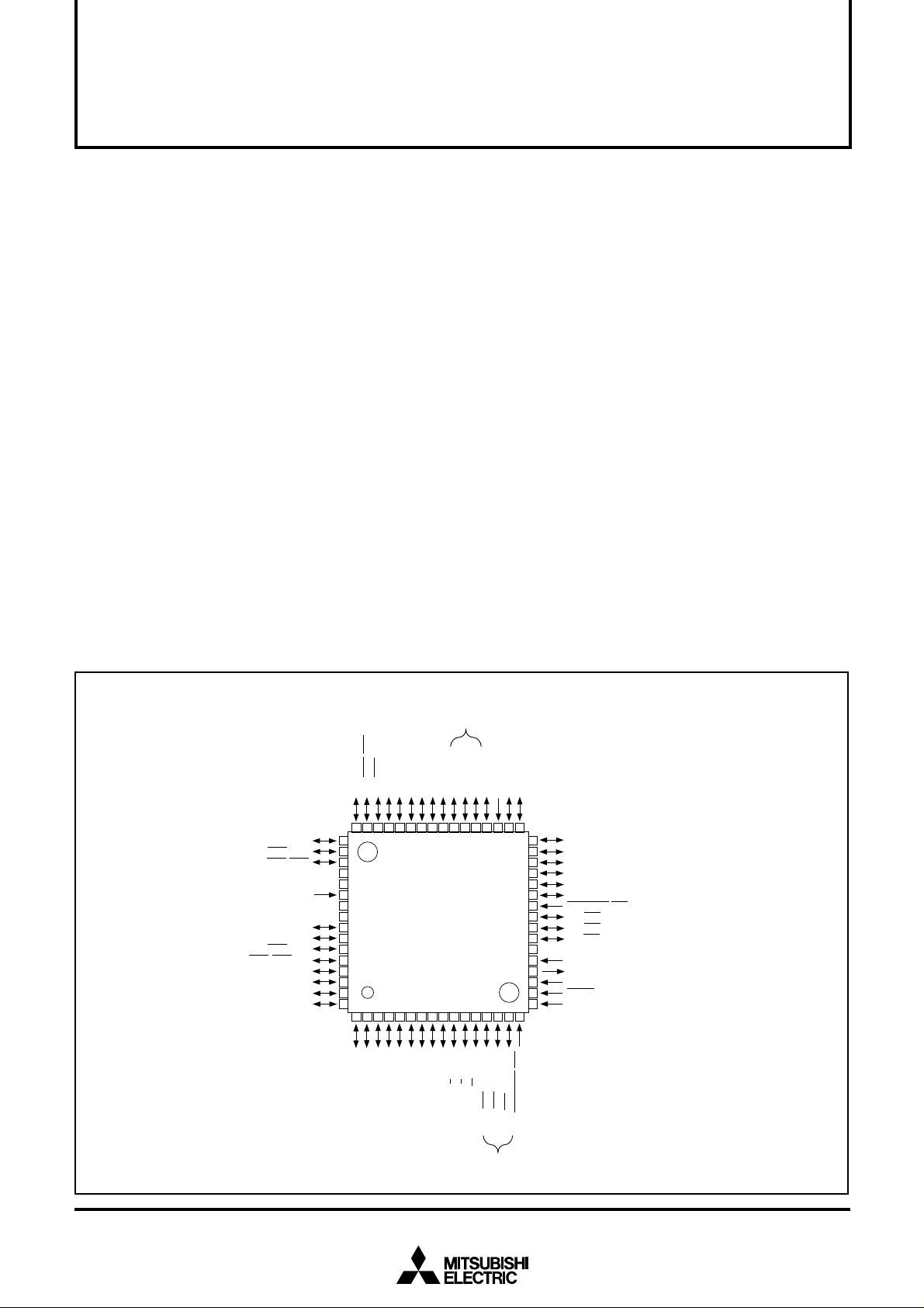
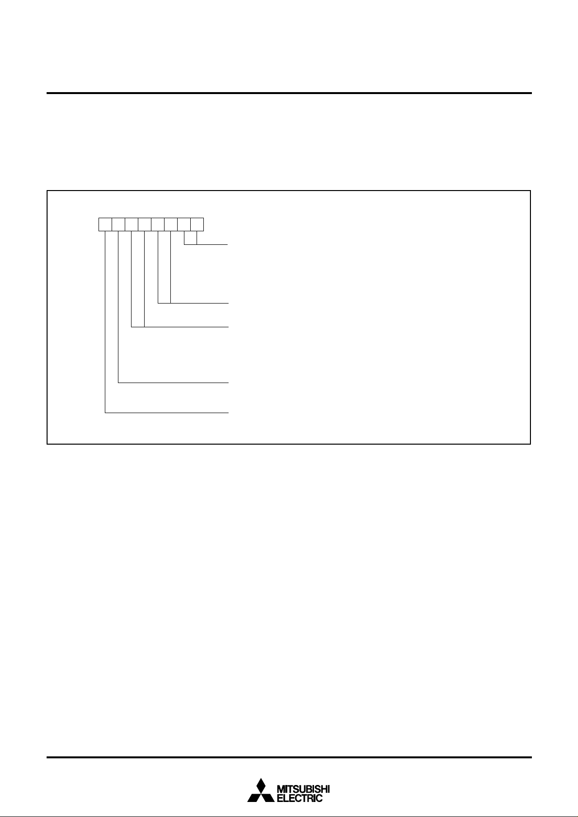
M37905MxC-XXXFP PIN CONFIGURATION (TOP VIEW)
0
P12/RXD
P11/CTS0/CLK
P10/CTS0/RTS
AV
V
AV
P83/AN11/TXD
P82/AN10/RXD
P81/AN9/CTS2/CLK
P80/AN8/CTS2/RTS2/DA
P77/AN7/DA
P76/AN
P75/AN
P74/AN
1
1
/CLK
/RTS
1
1
1
0
/RxD
/CTS
/CTS
/TxD
6
5
4
3
P1
P1
P1
P1
0
0
0
V
CC
CC
REF
SS
V
SS
2
2
2
1
0
6
5
4
48474645444342414039383736
49
50
51
52
53
54
55
56
M37905MXC-XXXFP
57
58
59
60
61
62
63
64
123456789
3
2
1
0
/AN
/AN
/AN
/AN
3
2
1
0
P7
P7
P7
P7
Outline 64P6N-A
OUT
1
/TA4
/TxD
0
7
P2
P1
2
3
/RTP1
/RTP1
IN
OUT
/TA3
7
/TA3
6
P6
P6
OUT
IN
/TA9
/TA4
2
1
P2
P2
0
1
/V/RTP1
/U/RTP1
IN
OUT
/TA2
5
/TA2
4
P6
P6
IN
/TA9
3
P2
3
/W/RTP0
IN
/TA1
3
P6
Note
)
)
IN
IN
(/TB1
(/TB0
5
4
P2
P2
10111213141516
2
1
/V/RTP0
/U/RTP0
IN
OUT
/TA0
1
/TA1
2
P6
P6
)
IN
(/TB2
6
P27P2
0
/IDU
IN
/W/RTP0
/TB2
7
OUT
/INT
7
/TA0
0
P5
P6
MD1
35
/IDV
IN
/TB1
6
/INT
6
P5
Note
1
/RTP2
/RTP2
IN
OUT
/TA5
/TA5
1
0
P4
P4
34
33
4
/IDW
/INT
IN
CUT
/TB0
5
P6OUT
/INT
5
P5
32
P42/TA6
OUT
/RTP2
CUT
2
3
OUT
/RTP3
0
1
OUT
/RTP3
2
3
/INT
0
1
TRG1
TRG0
31
30
29
28
27
26
25
24
23
22
21
20
19
18
17
P43/TA6IN/RTP2
P44/TA7
P45/TA7IN/RTP3
P46/TA8
P47/TA8IN/RTP3
P4OUT
P51/INT
P52/INT2/RTP
P53/INT3/RTP
V
SS
V
CONT
X
OUT
IN
X
RESET
MD0
Note : Allocation of pins TB0
can be switched by software.
IN to TB2IN
Page 2
M37905M4C-XXXFP, M37905M4C-XXXSP
M37905M6C-XXXFP, M37905M6C-XXXSP
PRELIMINARY
Notice: This is not a final specification.
Some parametric limits are subject to change.
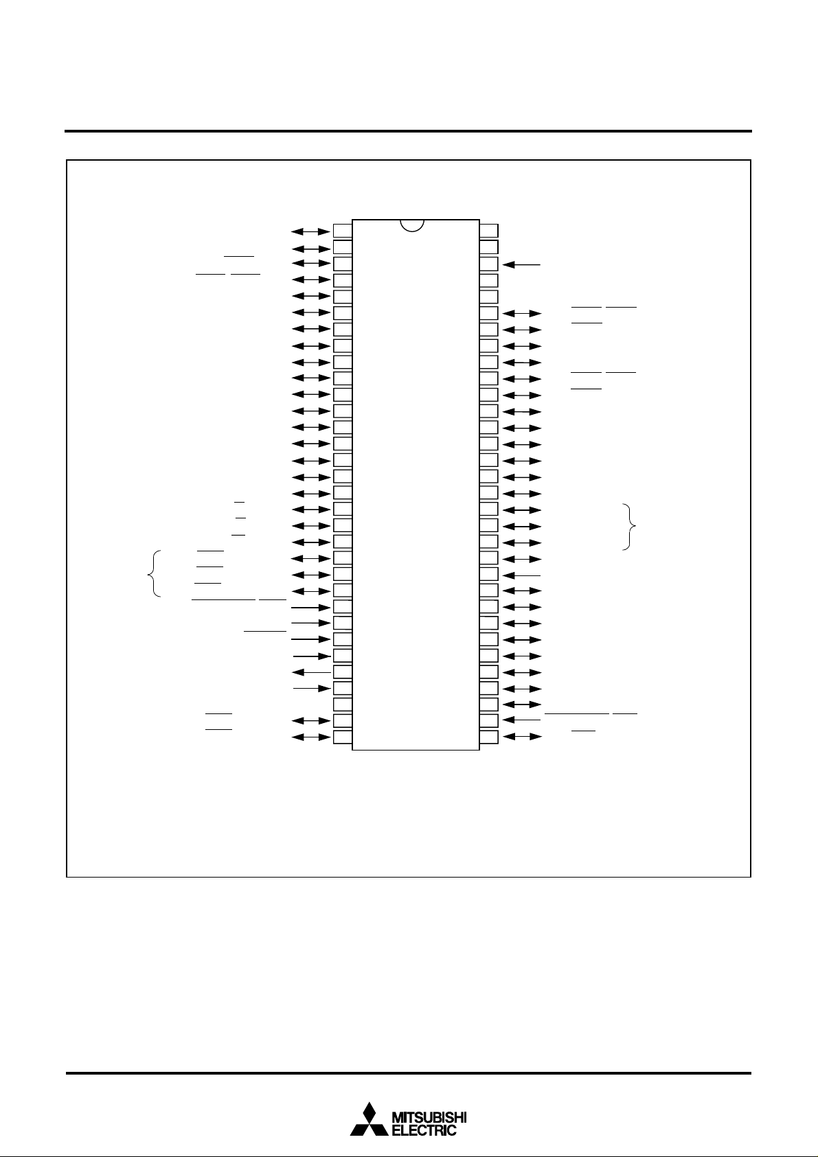
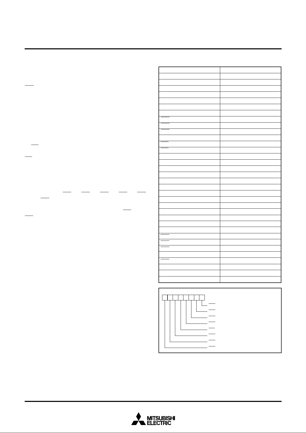
M37905MxC-XXXSP PIN CONFIGURATION (TOP VIEW)
2
/TxD
11
/AN
3
P8
2
/RxD
10
/AN
2
P8
P80/AN8/CTS
Note
P81/AN9/CTS2/CLK
2
/RTS2/DA1
P77/AN7/DA0
P76/AN6
P75/AN5
P74/AN4
P73/AN3
P72/AN2
P71/AN1
P70/AN0
P67/TA3IN/RTP13
P66/TA3OUT/RTP12
P65/TA2IN/U/RTP11
P64/TA2OUT/V/RTP10
P63/TA1IN/W/RTP03
P62/TA1OUT/U/RTP02
P61/TA0IN/V/RTP01
P60/TA0OUT/W/RTP00
P57/INT7/TB2IN/IDU
6/INT6/TB1IN/IDV
P5
5/INT5/TB0IN/IDW
P5
P6OUTCUT/INT4
P53/INT3/RTPTRG0
P52/INT2/RTPTRG1
MD0
RESET
XIN
XOUT
V
CONT
VSS
2
M37905M8C-XXXFP, M37905M8C-XXXSP
1
2
3
4
5
6
7
8
9
10
11
12
13
14
15
16
17
18
19
20
21
22
23
24
25
26
27
Outline 64P4B
28
29
30
31
32
M37905M
X
C-XXXSP
64
63
62
61
60
59
58
57
56
55
54
53
52
51
50
49
48
47
46
45
44
43
42
41
40
39
38
37
36
35
34
33
MITSUBISHI MICROCOMPUTERS
16-BIT CMOS MICROCOMPUTER
SS
V
AVSS
VREF
AVCC
VCC
P10/CTS0/RTS0
P11/CTS0/CLK0
P12/RxD0
P13/TxD0
P14/CTS1/RTS1
5/CTS1/CLK1
P1
P16/RxD1
P17/TxD1
P20/TA4OUT
P21/TA4IN
P22/TA9OUT
P23/TA9IN
P24(/TB0IN)
P25(/TB1IN)
6(/TB2IN)
P2
7
P2
Note
MD1
P40/TA5OUT/RTP20
P41/TA5IN/RTP21
P42/TA6OUT/RTP22
P43/TA6IN/RTP23
P44/TA7OUT/RTP30
P45/TA7IN/RTP31
P46/TA8OUT/RTP32
P47/TA8IN/RTP33
P4OUTCUT/INT0
P51/INT1
Note : Allocation of pins TB0IN to TB2IN
can be switched by software.
Outline 64P4B
2
Page 3
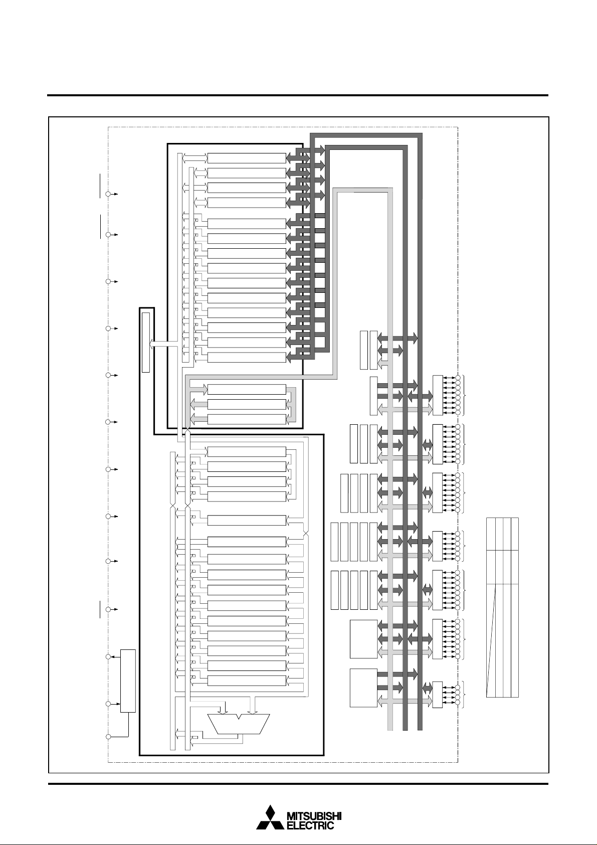
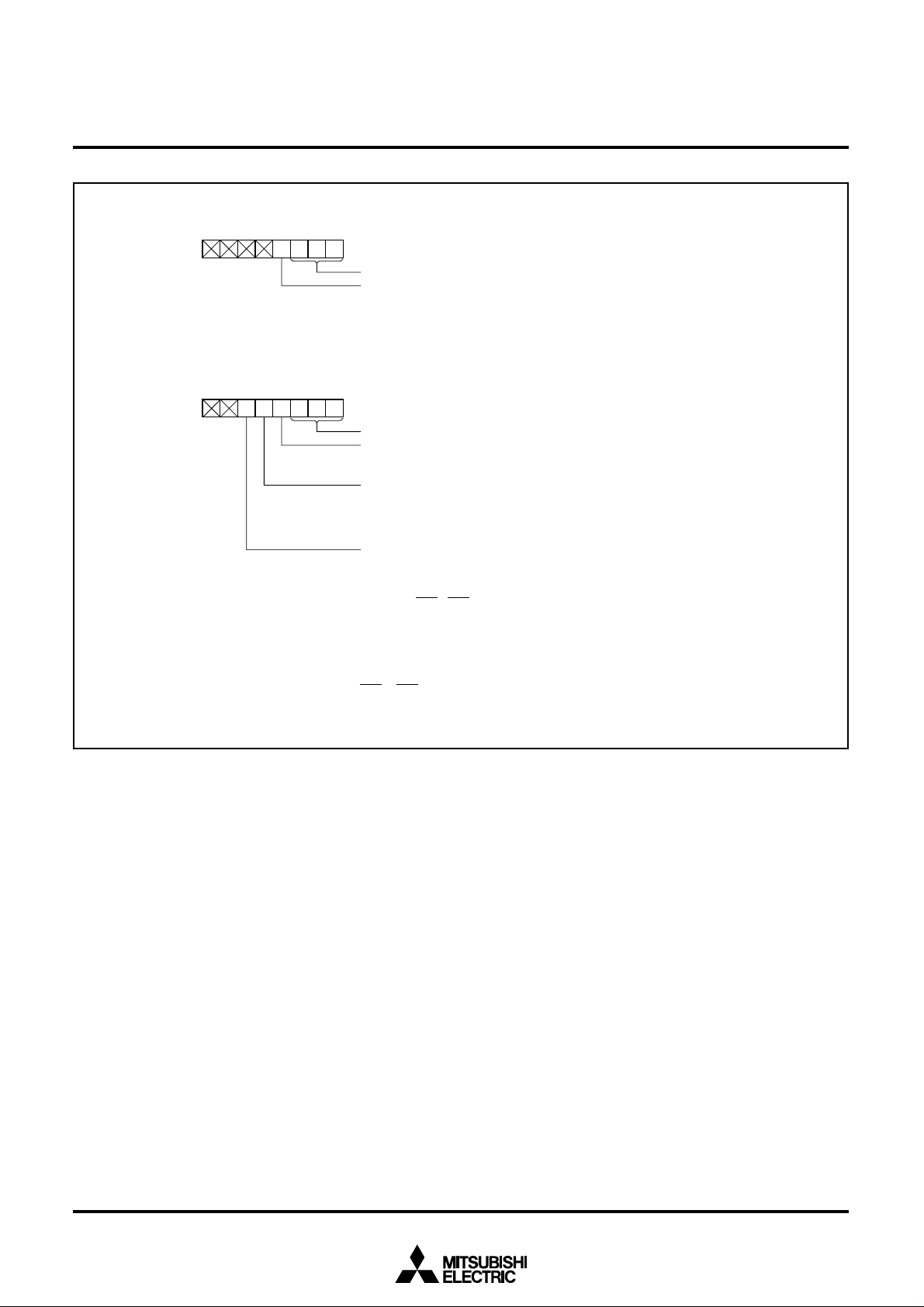
Central Processing Unit (CPU)
Bus
Interface
Unit
(BIU)
RESET
MD1
V
Reference
Voltage Input
Instruction Register (8)
REF
(0V)
AV
SS
AV
CC
V
CC
X
Clock input
Clock Generating Circuit
Reset inputClock output
IN
X
OUT
Address Bus
Data Bus (Odd)
Data Bus (Even)
A-D Converter (12)
UART1 (9)
UART0 (9)
Watchdog Timer
Timer TB1 (16)
Timer TB2 (16)
Timer TB0 (16)
D-A
1
Converter (8)
Timer TA1 (16)
Timer TA2 (16)
Timer TA3 (16)
Timer TA4 (16)
Timer TA0 (16)
RAM
(Note)
P6(8)
Input/Output P6
P5(6)
Input/Output P5
P7(8)
Input/Output P7
P4(8)
Input/Output P4
D-A
0
Converter (8)
P8(4)
Input/Output P8
MD0
(0V)
V
SS
P4OUT
CUT
ROM
(Note)
V
CONT
Timer TA6 (16)
Timer TA7 (16)
Timer TA8 (16)
Timer TA9 (16)
Timer TA5 (16)
P6OUT
CUT
P2(8)
Input/Output P2
P1(8)
Input/Output P1
UART2 (9)
M37905M4C-XXXFP, M37905M4C-XXXSP
M37905M6C-XXXFP, M37905M6C-XXXSP
M37905M8C-XXXFP, M37905M8C-XXXSP
ROM
32 Kbytes
48 Kbytes
60 Kbytes
RAM
1 Kbyte
3 Kbytes
3 Kbytes
Note:
Data Buffer DQ0 (8)
Data Buffer DQ
1
(8)
Data Buffer DQ
2
(8)
Data Buffer DQ
3
(8)
Instruction Queue Buffer Q
0
(8)
Instruction Queue Buffer Q
1
(8)
Instruction Queue Buffer Q
2
(8)
Instruction Queue Buffer Q
3
(8)
Instruction Queue Buffer Q
4
(8)
Instruction Queue Buffer Q
5
(8)
Instruction Queue Buffer Q
6
(8)
Instruction Queue Buffer Q
7
(8)
Instruction Queue Buffer Q
8
(8)
Instruction Queue Buffer Q
9
(8)
Program Address Register PA (24)
Data Address Register DA (24)
Incrementer (24)
Incrementer/Decrementer (24)
Input Buffer Register IB (16)
Program Counter PC (16)
Program Bank Register PG (8)
Processor Status Register PS (11)
Direct Page Register DPR0 (16)
Direct Page Register DPR1 (16)
Direct Page Register DPR2 (16)
Direct Page Register DPR3 (16)
Stack Pointer S (16)
Index Register Y (16)
Index Register X (16)
Accumulator B (16)
Accumulator A (16)
Arithmetic Logic
Unit (16)
Data Bank Register DT (8)
PRELIMINARY
Notice: This is not a final specification.
Some parametric limits are subject to change.
MITSUBISHI MICROCOMPUTERS
M37905M4C-XXXFP, M37905M4C-XXXSP
M37905M6C-XXXFP, M37905M6C-XXXSP
M37905M8C-XXXFP, M37905M8C-XXXSP
16-BIT CMOS MICROCOMPUTER
BLOCK DIAGRAM
3
Page 4
PRELIMINARY
Notice: This is not a final specification.
e param
Som
its are subject to change.
etric lim
FUNCTIONS
Number of basic machine instructions
Instruction execution time
External clock input frequency f(X
System clock frequency f(f
Memory size
Programmable input/output
ports
Multi-functional timers
Serial I/O
A-D converter
D-A converter
Dead-time timer
Watchdog timer
Interrupts
Clock generating circuit
PLL frequency multiplier
Power supply voltage
Power dissipation
Ports’ input/output
characteristics
Memory expansion
Operating ambient temperature range
Device structure
Package
sys)
M37905M4C-XXXFP, M37905M4C-XXXSP
M37905M6C-XXXFP, M37905M6C-XXXSP
M37905M8C-XXXFP, M37905M8C-XXXSP
IN)
ROM
RAM
P1, P2, P4, P6, P7
P5
P8
TA0–TA9
TB0–TB2
UART0, UART1, and UART2
Maskable interrups
Non-maskable interrups
nput/Output withstand voltage
utput current
MITSUBISHI MICROCOMPUTERS
16-BIT CMOS MICROCOMPUTER
FunctionsParameter
203
50 ns (the fastest instruction at f(f
20 MHz (Max.)
20 MHz (Max.)
(Note 1)
(Note 1)
8-bit ✕ 5
6-bit ✕ 1
4-bit ✕ 1
16-bit ✕ 10
16-bit ✕ 3
(UART or Clock synchronous serial I/O) ✕ 3
10-bit successive approximation method ✕ 1 (12 channels)
8-bit ✕ 2
8-bit ✕ 3
12-bit ✕ 1
8 external sources, 20 internal sources. Each interrupt can be set
to a priority level within the range of 0–7 by software.
3 internal sources
Incorporated (externally connected to a ceramic resonator or
quartz-crystal resonator).
The following multiplication ratios are available: ✕2, ✕3, ✕4.
5 V±0.5 V
125 mW (at f(fsys) = 20 MHz, Typ, ; the PLL frequency multiplier is inactive.)
5 V
5 mA
Not available (single-chip mode only).
–20 to 85 °C
CMOS high-performance silicon gate process
(Note 2)
sys) = 20 MHz)
Notes 1:
4
ROM
RAM
2:
Packages M37905M4C-XXXFP, M37905M6C-XXXFP, M37905M8C-XXXFP 64-pin plastic molded QFP (64P6N-A)
M37905M4C-XXXSP, M37905M6C-XXXSP, M37905M8C-XXXSP
M37905M4C-XXXFP, M37905M4C-XXXSP
M37905M6C-XXXFP, M37905M6C-XXXSP
M37905M8C-XXXFP, M37905M8C-XXXSP
M37905M4C-XXXFP, M37905M4C-XXXSP
M37905M6C-XXXFP, M37905M6C-XXXSP
M37905M8C-XXXFP, M37905M8C-XXXSP
32 Kbytes
48 Kbytes
60 Kbytes
1024 bytes
3072 bytes
3072 bytes
64-pin shrink plastic moldeds DIP (64P4B)
Page 5
PRELIMINARY
Notice: This is not a final specification.
e param
Som
its are subject to change.
etric lim
PIN DESCRIPTION
NamePin
Vcc, Vss
MD0
MD1
RESET
IN
X
XOUT
VCONT
AVcc,
AVss
REF
V
P10–P17
P20–P27
P40–P47
P51–P53,
P55–P57
P60–P67
P70–P77
P80–P83
P4OUTCUT
P6OUTCUT
Power supply input
MD0
MD1
Reset input
Clock input
Clock output
Filter circuit connection
Analog power supply input
Reference voltage input
I/O port P1
I/O port P2
I/O port P4
I/O port P5
I/O port P6
I/O port P7
I/O port P8
CUT input
P4OUT
P6OUT
CUT input
MITSUBISHI MICROCOMPUTERS
M37905M4C-XXXFP, M37905M4C-XXXSP
M37905M6C-XXXFP, M37905M6C-XXXSP
M37905M8C-XXXFP, M37905M8C-XXXSP
16-BIT CMOS MICROCOMPUTER
Input/
Output
—
Input
Input
Input
Input
Output
—
—
Input
I/O
I/O
I/O
I/O
I/O
I/O
I/O
Input
Input
Apply 5 V±0.5 V to Vcc, and 0 V to Vss.
Connect this pin to V
Connect this pin to Vss.
The microcomputer is reset when “L” level is applies to this pin.
These are input and output pins of the internal clock generating circuit. Connect a
ceramic resonator or quartz-crystal oscillator between pins X
external clock is used, the clock source should be connected to pin X
X
OUT should be left open.
When using the PLL frequency multiplier, connect this pin to the filter circuit. When
not using the PLL frequency multiplier, this pin should be left open.
Power supply input pins for the A-D and D-A converters. Connect AVcc to Vcc, and
AVss to Vss externally.
This is the reference voltage input pin for the A-D and D-A converters.
Port P1 is an 8-bit I/O port. This port has an I/O direction register, and each pin can
be programmed for input or output. These pins enter the input mode ar reset. These
pins also function as I/O pins of UART0, 1.
In addition to having the same functions as port P1, these pins function as I/O pins
for timers A4 and A9. Also, they can be programmed to function as input pins for timers B0 to B2.
In addition to having the same functions as port P1, these pins function as I/O pins
for timers A5 to A8. Also, they function as output pins for motor drive waveform.
In addition to having the same functions as port P1, these pins function as input pins
for INT
1 to INT3 and INT5 to INT7. Also, pins P55 to P57 function as input pins for
timers B0 to B2 and as input pins for position data in the three-phase waveform
mode; and pins P5
mode.
In addition to having the same functions as port P1, these pins function as I/O pins
for timers A0 to A3. Also, they function as motor drive waveform output pins.
In addition to having the same functions as port P1, these pins function as input pins
for the A-D converter. Also, P7
In addition to having the same functions as port P1, these pins function as input pins
for the A-D converter. Also, these pins function as I/O pins for UART2,and pin P8
functions as an output pin for the D-A converter.
This pin has the function to forcibly place port P4 pins in the input mode. Also, this
pin functions as an input pin for INT
forcibly cuts off a motor drive waveform output.
This pin has the function to forcibly place port P6 pins in the input mode. Also, this
pin functions as an input pin for INT
forcibly cuts off a motor drive waveform output.
SS.
2 and P53 function as trigger-input pins in the pulse output port
Functions
IN and XOUT. When an
7 functions as an output pin for the D-A converter.
0; and this pin is used to input a signal, which
4; and this pin is used to input a signal, which
IN, and pin
0
5
Page 6
PRELIMINARY
Notice: This is not a final specification.
Some parametric limits are subject to change.
MITSUBISHI MICROCOMPUTERS
M37905M4C-XXXFP, M37905M4C-XXXSP
M37905M6C-XXXFP, M37905M6C-XXXSP
M37905M8C-XXXFP, M37905M8C-XXXSP
16-BIT CMOS MICROCOMPUTER
BASIC FUNCTION BLOCKS
These microcomputers contain the following devices in the single
chip: ROM, RAM, CPU, bus interface unit, and peripheral devices
such as the interrupt control circuit, timers, serial I/O,
A-D converter, D-A converter, I/O ports, clock generating circuit, etc.
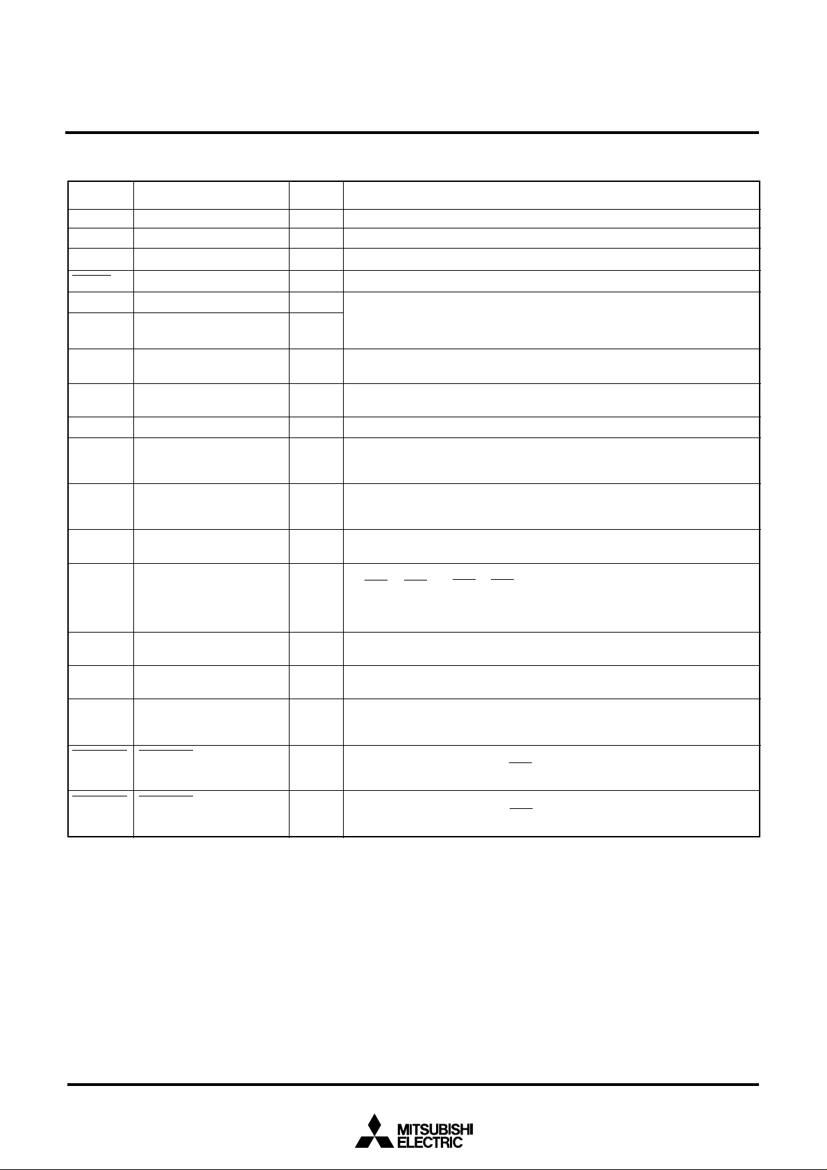
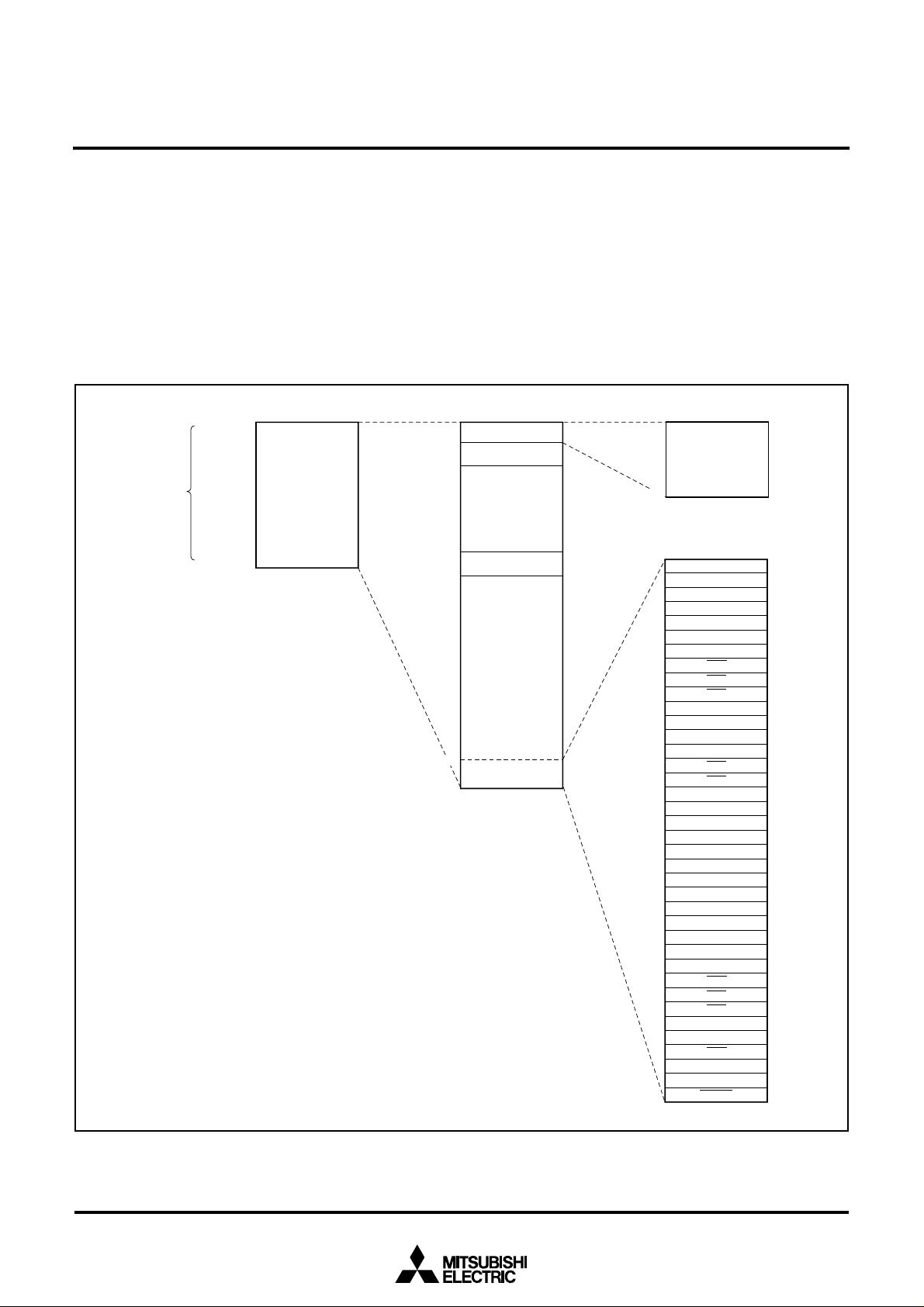
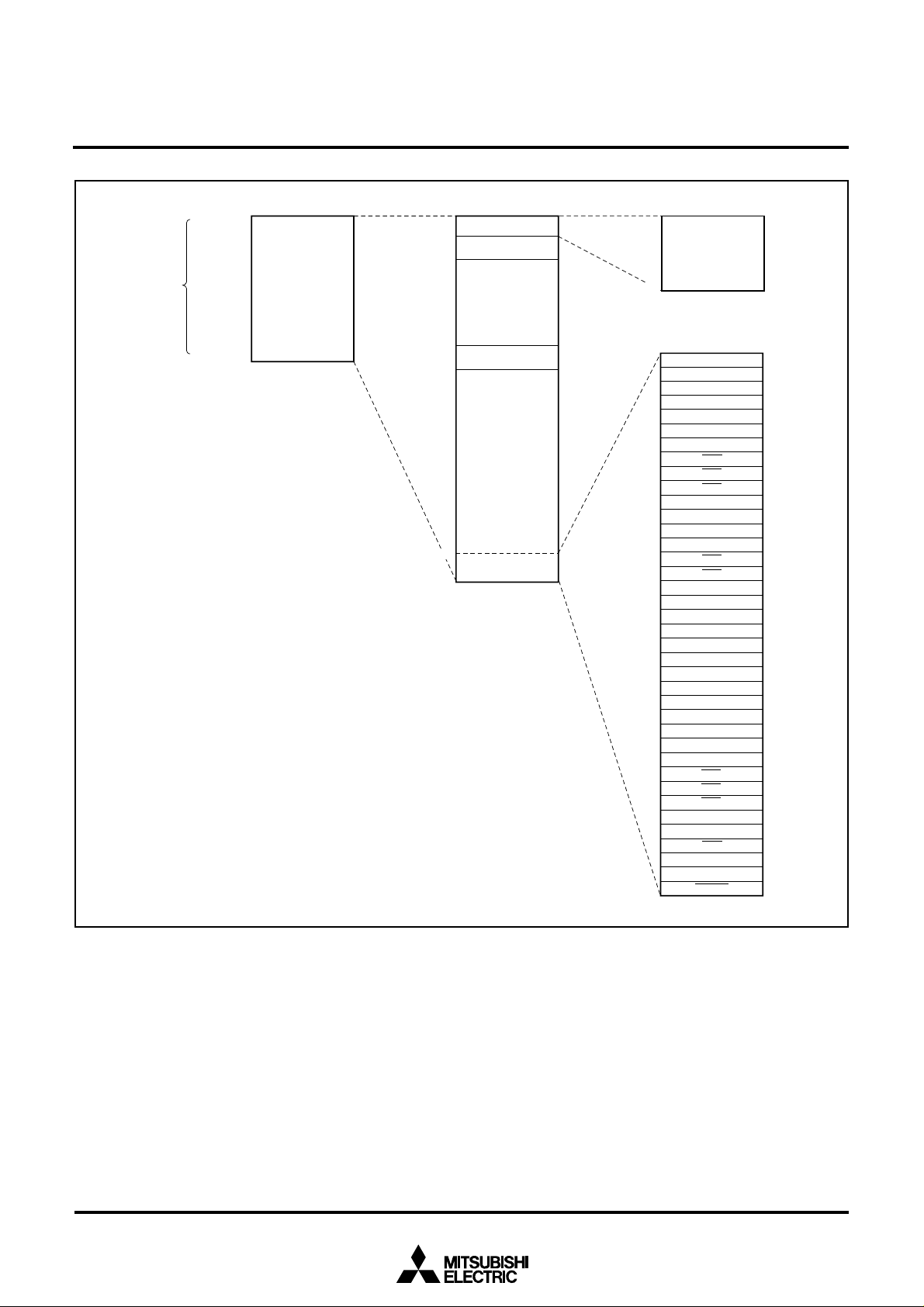
MEMORY
Figures 1 (1) through (3) show the memory maps. The address
space is 64 Kbytes from addresses 016 through FFFF16. This ad-
000000
Bank 0
16
16
00FFFF
16
000000
0000FF
000100
000BFF
000C00
000FFF
001000
007FFF
008000
00FFB4
00FFFF
dress space is called “bank 016”.
The internal ROM and RAM are allocated as shown in Figures 1 (1)
through (3).
Addresses FFB416 through FFFF16 contain the RESET and the interrupt vector addresses, and the interrupt vectors are stored there.
For details, refer to the section on interrupts.
Allocated to addresses 016 through FF16 are peripheral devices such
as I/O ports, A-D converter , D-A converter, serial I/O, timers, interrupt
control registers, etc. Figures 2 and 3 show the location of SFRs.
16
Peripheral devices'
control registers
16
16
16
16
16
16
16
16
16
16
Unused area
Internal RAM
1024 bytes
Unused area
Internal ROM
32 Kbytes
000000
0000FF
00FFB4
00FFFE
16
Peripheral devices'
control registers
(See Figures 2 and 3.)
16
Interrupt vector table
16
UART2 transmit
UART2 receive
Timer A9
Timer A8
Timer A7
Timer A6
Timer A5
INT
7
INT
6
INT
5
Reserved area
Address matching detect
Reserved area
Reserved area
INT
4
INT
3
A-D conversion
UART1 transmit
UART1 receive
UART0 transmit
UART0 receive
Timer B2
Timer B1
Timer B0
Timer A4
Timer A3
Timer A2
Timer A1
Timer A0
INT
2
INT
1
INT
0
Received area
Watchdog timer
DBC
BRK instruction
Zero divide
16
RESET
Fig. 1 (1) Memory map of M37905M4C-XXXFP/SP (Single-chip mode)
6
Page 7
PRELIMINARY
Notice: This is not a final specification.
Some parametric limits are subject to change.
000000
16
Bank 0
16
00FFFF
16
MITSUBISHI MICROCOMPUTERS
M37905M4C-XXXFP, M37905M4C-XXXSP
M37905M6C-XXXFP, M37905M6C-XXXSP
M37905M8C-XXXFP, M37905M8C-XXXSP
16-BIT CMOS MICROCOMPUTER
000000
0000FF
000100
0003FF
000400
000FFF
001000
003FFF
004000
00FFB4
00FFFF
Peripheral devices'
16
control registers
16
16
16
16
16
16
16
16
16
16
Unused area
Internal RAM
3072 bytes
Unused area
Internal ROM
48 Kbytes
000000
0000FF
00FFB4
00FFFE
16
Peripheral devices'
control registers
(See Figures 2 and 3.)
16
Interrupt vector table
16
UART2 transmit
UART2 receive
Timer A9
Timer A8
Timer A7
Timer A6
Timer A5
INT
7
INT
6
INT
5
Reserved area
Address matching detect
Reserved area
Reserved area
INT
4
INT
3
A-D conversion
UART1 transmit
UART1 receive
UART0 transmit
UART0 receive
Timer B2
Timer B1
Timer B0
Timer A4
Timer A3
Timer A2
Timer A1
Timer A0
INT
2
INT
1
INT
0
Reserved area
Watchdog timer
DBC
BRK instruction
Zero divide
16
RESET
Fig. 1 (2) Memory map of M37905M6C-XXXFP/SP (Single-chip mode)
7
Page 8
PRELIMINARY
Notice: This is not a final specification.
Some parametric limits are subject to change.
000000
16
Bank 0
16
00FFFF
16
MITSUBISHI MICROCOMPUTERS
M37905M4C-XXXFP, M37905M4C-XXXSP
M37905M6C-XXXFP, M37905M6C-XXXSP
M37905M8C-XXXFP, M37905M8C-XXXSP
16-BIT CMOS MICROCOMPUTER
000000
16
0000FF
000100
0003FF
000400
000FFF
001000
00FFB4
00FFFF
Peripheral devices'
control registers
16
16
16
16
Internal RAM
16
16
Internal ROM
16
16
Unused area
3072 bytes
60 Kbytes
000000
0000FF
00FFB4
00FFFE
16
Peripheral devices'
control registers
(See Figures 2 and 3.)
16
Interrupt vector table
16
UART2 transmit
UART2 receive
Timer A9
Timer A8
Timer A7
Timer A6
Timer A5
INT
7
INT
6
5
INT
Reserved area
Address matching detect
Reserved area
Reserved area
INT
4
INT
3
A-D conversion
UART1 transmit
UART1 receive
UART0 transmit
UART0 receive
Timer B2
Timer B1
Timer B0
Timer A4
Timer A3
Timer A2
Timer A1
Timer A0
INT
2
INT
1
INT
0
Reserved area
Watchdog timer
DBC
BRK instruction
Zero divide
16
RESET
Fig. 1 (3) Memory map of M37905M8C-XXXFP/SP (Single-chip mode)
8
Page 9
PRELIMINARY
Notice: This is not a final specification.
Some parametric limits are subject to change.
Address (Hexadecimel notation) Address (Hexadecimel notation)
000000
000001
000002
000003
000004
000005
000006
000007
000008
000009
00000A
00000B
00000C
00000D
00000E
00000F
000010
000011
000012
000013
000014
000015
000016
000017
000018
000019
00001A
00001B
00001C
00001D
00001E
00001F
000020
000021
000022
000023
000024
000025
000026
000027
000028
000029
00002A
00002B
00002C
00002D
00002E
00002F
000030
000031
000032
000033
000034
000035
000036
000037
000038
000039
00003A
00003B
00003C
00003D
00003E
00003F
Reserved area (Note)
16
Reserved area (Note)
16
Reserved area (Note)
16
Port P1 register
16
Reserved area (Note)
16
Port P1 direction register
16
16
Port P2 register
Reserved area (Note)
16
16
Port P2 direction register
Reserved area (Note)
16
Port P4 register
16
16
Port P5 register
16
Port P4 direction register
16
Port P5 direction register
16
Port P6 register
16
Port P7 register
16
Port P6 direction register
16
Port P7 direction register
16
Port P8 register
16
16
Port P8 direction register
16
Reserved area (Note)
16
Reserved area (Note)
16
Reserved area (Note)
16
Reserved area (Note)
16
16
16
16
16
16
A-D control register 0
16
A-D control register 1
16
A-D register 0
16
16
A-D register 1
16
16
A-D register 2
16
16
A-D register 3
16
16
A-D register 4
16
16
A-D register 5
16
16
A-D register 6
16
16
A-D register 7
16
16
UART0 transmit/receive mode register
16
UART0 band rate register (BRG0)
16
UART0 transmit buffer register
16
16
UART0 transmit/receive control register 0
16
UART0 transmit/receive control register 1
16
UART0 receive buffer register
16
16
UART1 transmit/receive mode register
16
UART1 baud rate register (BRG1)
16
UART1 transmit buffer register
16
16
UART1 transmit/receive control register 0
16
UART1 transmit/receive control register 1
16
UART1 receive buffer register
16
MITSUBISHI MICROCOMPUTERS
M37905M4C-XXXFP, M37905M4C-XXXSP
M37905M6C-XXXFP, M37905M6C-XXXSP
M37905M8C-XXXFP, M37905M8C-XXXSP
16-BIT CMOS MICROCOMPUTER
16
000040
000041
000042
000043
000044
000045
000046
000047
000048
000049
00004A
00004B
00004C
00004D
00004E
00004F
000050
000051
000052
000053
000054
000055
000056
000057
000058
000059
00005A
00005B
00005C
00005D
00005E
00005F
000060
000061
000062
000063
000064
000065
000066
000067
000068
000069
00006A
00006B
00006C
00006D
00006E
00006F
000070
000071
000072
000073
000074
000075
000076
000077
000078
000079
00007A
00007B
00007C
00007D
00007E
00007F
Count start register 0
16
Count start register 1
16
One-shot start register 0
One-shot start register 1
16
Up-down register 0
16
Timer A clock division select register
16
16
Timer A0 register
16
16
Timer A1 register
16
16
Timer A2 register
16
16
Timer A3 register
16
16
Timer A4 register
16
16
Timer B0 register
16
16
Timer B1 register
16
16
Timer B2 register
16
Timer A0 mode register
16
Timer A1 mode register
16
Timer A2 mode register
16
Timer A3 mode register
16
16
Timer A4 mode register
16
Timer B0 mode register
16
Timer B1 mode register
16
Timer B2 mode register
Processor mode register 0
16
Processor mode register 1
16
16
Watchdog timer register
Watchdog timer frequency select register
16
16
Particular function select register 0
Particular function select register 1
16
16
Particular function select register 2
Reserved area (Note)
16
16
Debug control register 0
Debug control register 1
16
16
Address comparison register 0
16
16
16
Address comparison register 1
16
16
interrupt control register
16
3
INT
16
interrupt control register
INT
4
16
A-D conversion interrupt
16
UART0 transmit interrupt
16
UART0 receive interrupt
16
UART1 transmit interrupt
16
UART1 receive interrupt
16
Timer A0 interrupt
16
Timer A1 interrupt
16
Timer A2 interrupt
16
Timer A3 interrupt
16
Timer A4 interrupt
16
Timer B0 interrupt
16
Timer B1 interrupt
16
Timer B2 interrupt
16
0
INT
16
1
INT
16
2
INT
interrupt
interrupt
interrupt
control register
control register
control register
control register
control register
control register
control register
control register
control register
control register
control register
control register
control register
control register
control register
control register
Fig. 2 Location of SFRs (1)
Note: Do not write to this address.
9
Page 10
PRELIMINARY
Notice: This is not a final specification.
Some parametric limits are subject to change.
Address (Hexadecimel notation) Address (Hexadecimel notation)
000080
000081
000082
000083
000084
000085
000086
000087
000088
000089
00008A
00008B
00008C
00008D
00008E
00008F
000090
000091
000092
000093
000094
000095
000096
000097
000098
000099
00009A
00009B
00009C
00009D
00009E
00009F
0000A0
0000A1
0000A2
0000A3
0000A4
0000A5
0000A6
0000A7
0000A8
0000A9
0000AA
0000AB
0000AC
0000AD
0000AE
0000AF
0000B0
0000B1
0000B2
0000B3
0000B4
0000B5
0000B6
0000B7
0000B8
0000B9
0000BA
0000BB
0000BC
0000BD
0000BE
0000BF
Reserved area (Note)
16
Reserved area (Note)
16
Reserved area (Note)
16
Reserved area (Note)
16
Reserved area (Note)
16
Reserved area (Note)
16
Reserved area (Note)
16
16
Reserved area (Note)
16
16
Reserved area (Note)
16
16
Reserved area (Note)
16
16
Reserved area (Note)
16
16
Reserved area (Note)
16
16
16
Reserved area (Note)
16
16
External interrupt input read-out register
16
D-A control register
16
16
D-A register 0
16
D-A register 1
16
16
16
16
16
16
16
16
Pulse output control register
16
16
Pulse output data register 0
16
Pulse output data register 1
16
16
16
Waveform output mode register
16
Dead-time timer
16
Three-phase output data register 0
16
Three-phase output data register 1
Position-data-retain function control register
16
16
Serial I/O pin control register
16
16
16
Port P2 pin
16
16
UART2 transmit/receive mode register
16
UART2 band rate register (BRG2)
16
UART2 transmit buffer register
16
UART2 transmit/receive control register 0
16
UART2 transmit/receive control register 1
16
16
UART2 receive buffer register
16
Reserved area (Note)
16
16
Reserved area (Note)
16
Reserved area (Note)
16
Clock control register 0
16
Reserved area (Note)
16
Reserved area (Note)
16
Reserved area (Note)
16
function control register
MITSUBISHI MICROCOMPUTERS
M37905M4C-XXXFP, M37905M4C-XXXSP
M37905M6C-XXXFP, M37905M6C-XXXSP
M37905M8C-XXXFP, M37905M8C-XXXSP
16-BIT CMOS MICROCOMPUTER
0000C0
16
0000C1
16
0000C2
16
0000C3
16
0000C4
16
0000C5
0000C6
0000C7
0000C8
0000C9
0000CA
0000CB
0000CC
0000CD
0000CE
0000CF
0000D0
0000D1
0000D2
0000D3
0000D4
0000D5
0000D6
0000D7
0000D8
0000D9
0000DA
0000DB
0000DC
0000DD
0000DE
0000DF
0000E0
0000E1
0000E2
0000E3
0000E4
0000E5
0000E6
0000E7
0000E8
0000E9
0000EA
0000EB
0000EC
0000ED
0000EE
0000EF
0000F0
0000F1
0000F2
0000F3
0000F4
0000F5
0000F6
0000F7
0000F8
0000F9
0000FA
0000FB
0000FC
0000FD
0000FE
0000FF
Up-down register
16
16
Timer A5 register
16
16
16
16
16
16
16
16
16
16
16
16
16
16
16
16
16
16
16
16
16
16
16
16
16
16
16
16
16
16
16
16
16
16
16
16
16
16
16
16
16
16
16
16
16
16
16
16
16
16
16
16
16
16
16
16
16
A6
Timer
A7
Timer
A8
Timer
A9
Timer
A01 register
Timer
A11 register
Timer
A21 register
Timer
A5 mode register
Timer
Timer
A6 mode register
Timer
A7 mode register
Timer
A8 mode register
Timer
A9 mode register
A-D control register 2
Comparator function select register 0
Comparator function select register 1
Comparator result register 0
Comparator result register 1
A-D register 8
A-D register 9
A-D register 10
A-D register 11
Reserved area (Note)
Reserved area (Note)
Reserved area (Note)
Reserved area (Note)
Reserved area (Note)
Reserved area (Note)
Reserved area (Note)
Reserved area (Note)
UART2 transmit interrupt
UART2 receive interrupt
Timer A5
Timer A6
Timer A7
Timer A8
Timer A9
INT5 interrupt
INT6 interrupt
INT7 interrupt
register
register
register
register
interrupt
interrupt
interrupt
interrupt
interrupt
control register
control register
control register
1
control register
control register
control register
control register
control register
control register
control register
Note: Do not write to this address.
Fig. 3 Location of SFRs (2)
10
Page 11
PRELIMINARY
Notice: This is not a final specification.
Some parametric limits are subject to change.
MITSUBISHI MICROCOMPUTERS
M37905M4C-XXXFP, M37905M4C-XXXSP
M37905M6C-XXXFP, M37905M6C-XXXSP
M37905M8C-XXXFP, M37905M8C-XXXSP
16-BIT CMOS MICROCOMPUTER
CENTRAL PROCESSING UNIT (CPU)
The CPU has 13 registers and is shown in Figure 4. Each of these
registers is described below.
ACCUMULATOR A (A)
Accumulator A is the main register of the microcomputer. It consists
of 16 bits and the low-order 8 bits can be used separately. Data
length flag m determines whether the register is used as 16-bit register or as 8-bit register. It is used as a 16-bit register when flag m is
“0” and as an 8-bit register when flag m is “1”. Flag m is a part of the
processor status register (PS) which is described later.
Data operations such as calculations, data transfer, input/output,
etc., are executed mainly through accumulator A.
ACCUMULATOR B (B)
Accumulator B has the same functions as accumulator A, but the use
of accumulator B requires more instruction bytes and execution
cycles than accumulator A.
ACCUMULATOR E
Accumulator E is a 32-bit register and consists of accumulator A
(low-order 16 bits) and accumulator B (high-order 16 bits). It is used
for 32-bit data processing.
INDEX REGISTER X (X)
Index register X consists of 16 bits and the low-order 8 bits can be
used separately. Index register length flag x determines whether the
register is used as 16-bit register or as 8-bit register. It is used as a
16-bit register when flag x is “0” and as an 8-bit register when flag x
is “1”. Flag x is a part of the processor status register (PS) which is
described later.
In index addressing modes in which register X is used as the index
register, the contents of this address are added to obtain the real address.
Index register X functions as a pointer register which indicates an
address of data table in instructions MVP, MVN, RMPA (Repeat
MultiPly and Accumulate).
INDEX REGISTER Y (Y)
Index register Y consists of 16 bits and the low-order 8 bits can be
used separately. The index register length flag x determines whether
the register is used as 16-bit register or as 8-bit register. It is used as
a 16-bit register when flag x is “0” and as an 8-bit register when flag
x is “1”. Flag x is a part of the processor status register (PS) which is
described later.
In index addressing modes in which register Y is used as the index
register, the contents of this address are added to obtain the real address.
Index register Y functions as a pointer register which indicates an
address of data table in instructions MVP, MVN, RMPA (Repeat
MultiPly and Accumulate).
15 7 0
31
70
PG Program bank register PG
70
Fig. 4 Register structure
B
H
Accumulator B
Data bank register DTDT
B
L
Accumulator A
15 7 0
Accumulator E
15 7 0
15 7 0
15
15 7 0
15 0
15 0
15 0
15
00000
A
A
H
B
H
X
H
Y
H
H
IPL2IPL1IPL
7
S
PC
DPR0 to DPR3
7
0
NVmxDIZC
A
L
A
L
B
L
X
L
Y
L
0
0
Index register X
Index register Y
Stack pointer S
Program counter PC
Direct page registers DPR0 to DPR3
0
Processor status register PS
Carry flag
Zero flag
Interrupt disable flag
Decimal mode flag
Index register length flag
Data length flag
Overflow flag
Negative flag
Processor interrupt priority level IPL
11
Page 12

PRELIMINARY
Notice: This is not a final specification.
Some parametric limits are subject to change.
MITSUBISHI MICROCOMPUTERS
M37905M4C-XXXFP, M37905M4C-XXXSP
M37905M6C-XXXFP, M37905M6C-XXXSP
M37905M8C-XXXFP, M37905M8C-XXXSP
16-BIT CMOS MICROCOMPUTER
STACK POINTER (S)
Stack pointer (S) is a 16-bit register. It is used during a subroutine
call or interrupts. It is also used during stack, stack pointer relative,
or stack pointer relative indirect indexed Y addressing mode.
PROGRAM COUNTER (PC)
Program counter (PC) is a 16-bit counter that indicates the low-order
16 bits of the next program memory address to be executed. There
is a bus interface unit between the program memory and the CPU,
so that the program memory is accessed through bus interface unit.
This is described later.
PROGRAM BANK REGISTER (PG)
Program bank register is an 8-bit register that indicates the high-order 8 bits of the next program memory address to be executed.
When a carry occurs by incrementing the contents of the program
counter, the contents of the program bank register (PG) is increased
by 1. Also, when a carry or borrow occurs after adding or subtracting
the offset value to or from the contents of the program counter (PC)
using the branch instruction, the contents of the program bank register (PG) is increased or decreased by 1, so that programs can be
written without worrying about bank boundaries.
DATA BANK REGISTER (DT)
Data bank register (DT) is an 8-bit register. With some addressing
modes, the data bank register (DT) is used to specify a part of the
memory address. The contents of data bank register (DT) is used as
the high-order 8 bits of a 24-bit address. Addressing modes that use
the data bank register (DT) are direct indirect, direct indexed X indirect, direct indirect indexed Y, absolute, absolute bit, absolute indexed X, absolute indexed Y, absolute bit relative, and stack pointer
relative indirect indexed Y.
DIRECT PAGE REGISTERS 0 through 3
(DPR0 through DPR3)
The direct page register is a 16-bit register. An addressing mode of
which name includes ‘direct’ generates an address of data to be accessed, regarding the contents of this register as the base address.
The 7900 Series has been expanded direct page registers up to 4
(DPR0 to DPR3), in comparison to the 7700 Series which has the
single direct page register. Accordingly, the 7900 Series’s direct addressing method which uses direct page registers differs from that of
the 7700 Series. However, the conventional direct addressing
method, using only DPR0, is still be selectable, in order to make use
of the 7700 Series software property. For more details, refer to the
section on the direct page.
PROCESSOR STATUS REGISTER (PS)
Processor status register (PS) is an 11-bit register. It consists of
flags to indicate the result of operation and CPU interrupt levels.
Branch operations can be performed by testing the flags C, Z, V , and
N.
The details of each bit of the processor status register are described
below.
1. Carry flag (C)
The carry flag contains the carry or borrow generated by the ALU after an arithmetic operation. This flag is also affected by shift and rotate instructions. This flag can be set and reset directly with the SEC
and CLC instructions or with the SEP and CLP instructions.
2. Zero flag (Z)
The zero flag is set if the result of an arithmetic operation or data
transfer is zero and reset if it is not. This flag can be set and reset
directly with the SEP and CLP instructions.
3. Interrupt disable flag (I)
When the interrupt disable flag is set to “1”, all interrupts except
watchdog timer and software interrupts are disabled. This flag is set
to “1” automatically when an interrupt is accepted. It can be set and
reset directly with the SEI and CLI instructions or SEP and CLP instructions.
4. Decimal mode flag (D)
The decimal mode flag determines whether addition and subtraction
are performed as binary or decimal. Binary arithmetic is performed
when this flag is “0”. If it is “1”, decimal arithmetic is performed with
each word treated as 2- or 4- digit decimal. Arithmetic operation is
performed using four digits when data length flag m is “0” and with
two digits when it is “1”. Decimal adjust is automatically performed.
(Decimal operation is possible only with the ADC and SBC instructions.) This flag can be set and reset with the SEP and CLP instructions.
12
Page 13

M37905M4C-XXXFP, M37905M4C-XXXSP
M37905M6C-XXXFP, M37905M6C-XXXSP
PRELIMINARY
Notice: This is not a final specification.
Some parametric limits are subject to change.
5. Index register length flag (x)
The index register length flag determines whether index register X
and index register Y are used as 16-bit registers or as 8-bit registers.
The registers are used as 16-bit registers when flag x is “0” and as 8bit registers when it is “1”.
This flag can be set and reset with the SEP and CLP instructions.
6. Data length flag (m)
The data length flag determines whether the data length is 16-bit or
8-bit. The data length is 16 bits when flag m is “0” and 8 bits when it
is “1”. This flag can be set and reset with the SEM and CLM instructions or with the SEP and CLP instructions.
7. Overflow flag (V)
The overflow flag is valid when addition or subtraction is performed
with a word treated as a signed binary number. If data length flag m
is “0”, the overflow flag is set when the result of addition or subtraction is outside the range between –32768 and +32767. If data length
flag m is “1”, the overflow flag is set when the result of addition or
subtraction is outside the range between –128 and +127. It is reset
in all other cases. The overflow flag can also be set and reset directly
with the SEP, and CLV or CLP instructions.
Additionally, the overflow flag is set when a result of unsigned/signed
division exceeds the length of the register where the result is to be
stored; the flag is also set when the addition result is outside range
of –2147483648 to +2147483647 in the RMPA operation.
M37905M8C-XXXFP, M37905M8C-XXXSP
MITSUBISHI MICROCOMPUTERS
16-BIT CMOS MICROCOMPUTER
8. Negative flag (N)
The negative flag is set when the result of arithmetic operation or
data transfer is negative (If data length flag m is “0”, data’s bit 15 is
“1”. If data length flag m is “1”, data’s bit 7 is “1”.) It is reset in all other
cases. It can also be set and reset with the SEP and CLP instructions.
9. Processor interrupt priority level (IPL)
The processor interrupt priority level (IPL) consists of 3 bits and determines the priority of processor interrupts from level 0 to level 7.
Interrupt is enabled when the interrupt priority of the device requesting interrupt (set using the interrupt control register) is higher than
the processor interrupt priority . When an interrupt is enabled, the current processor interrupt priority level is saved in a stack and the processor interrupt priority level is replaced by the interrupt priority level
of the device requesting the interrupt. Refer to the section on interrupts for more details.
Note: Fix bits 11 to 15 of the processor status register (PS) to “0”.
13
Page 14

PRELIMINARY
Notice: This is not a final specification.
Some parametric limits are subject to change.
MITSUBISHI MICROCOMPUTERS
M37905M4C-XXXFP, M37905M4C-XXXSP
M37905M6C-XXXFP, M37905M6C-XXXSP
M37905M8C-XXXFP, M37905M8C-XXXSP
16-BIT CMOS MICROCOMPUTER
BANK
In order to effectively use the integrated hardware on the chip, this
CPU core uses an address generating method with a 24-bit address
split into high-order 8 bits and low-order 16 bits. In other words, the
64 Kbytes specified by the low-order 16 bits are one unit (referred to
as “bank”), and the address space is divided into 256 banks (016 to
FF16) specified by the high-order 8 bits.
In the program area on the address space, the bank is specified by
the program bank register (PG), and the address in the bank is
specified by the program counter (PC).
As for each bank boundary, when an overflow has occurred in PC,
the contents of PG are incremented by 1. When a borrow has occurred in PC, the contents of PG are decremented by 1. Under the
normal conditions, therefore, programming without concern for the
bank boundaries is possible. Furthermore, as for the data area on
the address space, the bank is specified by the data bank register
(DT), and the address in the bank is specified by the operation result
by using the various addressing modes (Note).
Note: Some addressing modes directly specify a bank.
DIRECT PAGE
The internal memory and control registers for internal peripheral devices, etc. are assigned to bank 016 (addresses 016 to FFFF16). The
direct page and direct addressing modes have been provided for the
effective access to bank 016. In the 7900 Series, two types of direct
addressing modes are available: the conventional direct addressing
mode which uses only DPR0, as in the 7700 Series, and the expanded direct addressing mode, which uses up to 4 direct page registers as selected by the user. The addressing mode is selected
according to the contents of bit 1 of the processor mode register 1.
This bit 1 is cleared to “0” at reset. (In other words, the conventional
direct addressing mode is selected.) However, once this bit 1 has
been set to “1” by software, this bit cannot be cleared to “0” again,
except by reset. That is to say , when one of these two direct addressing modes has been selected just after reset, the selected addressing mode cannot be switched to another one while the program is
running.
Refer to “7900 Series Software Manual” for details concerning the
various addressing modes which use the direct page area.
Instruction Set
The CPU core of the 7900 Series has an expanded instruction set
based on the existing 7700/7751 Series’ CPU core. In addition, its
source code (mnemonic) has the complete upper compatibility with
the 7700 Series instruction set.
For details concerning addressing modes and instruction set, refer to
“7900 Series Software Manual”.
■ Conventional direct addressing mode
The direct page area consists of 256-byte space. Its bank address is
“0016”, and the base address of its low-order 16-bit address is specified by the contents of the direct page register 0 (DPR0). In this conventional direct addressing modes, a value (1 byte) just after an
instruction code is regarded as an offset value for the DPR0 contents, and the CPU accesses each address in the direct page area.
■ Expanded direct addressing mode
The direct page area consists of four 64-byte spaces. Their bank
address is “0016”, and the four base addresses of their low-order 16bit addresses are respectively specified by the contents of four direct
page registers. In this expanded direct addressing mode, a value (1
byte) just after an instruction code is regarded as follows:
• High-order 2 bits: regarded as a selection field for DPR0 to DPR3.
• Low-order 6 bits: regarded as an offset value for the selected direct
page register.
Then, the CPU accesses each address in each direct page area:
14
Page 15
PRELIMINARY
Notice: This is not a final specification.
Some parametric limits are subject to change.
MITSUBISHI MICROCOMPUTERS
M37905M4C-XXXFP, M37905M4C-XXXSP
M37905M6C-XXXFP, M37905M6C-XXXSP
M37905M8C-XXXFP, M37905M8C-XXXSP
16-BIT CMOS MICROCOMPUTER
BUS INTERFACE UNIT
Data transfer between the central processing unit (CPU) and internal memory, internal peripheral devices is always performed via the
bus interface unit (BIU), which is located between the CPU and the
internal buses.
Figure 5 shows the BIU and the bus structure. The CPU and BIU are
connected by a dedicated bus, and any transfer between the CPU
and BIU is controlled by this dedicated bus.
On the other hand, data transfer between the BIU and internal pe-
M37905
CPU bus
Central
Processing
Unit
(CPU)
Bus
Interface
Unit
(BIU)
ripheral devices uses the following internal common buses: 32-bit
code bus, 16-bit data bus, 24-bit address bus, and control signals.
The bus control method where the code bus and the data bus separate out (hereafter, this method is referred to as the separate code/
data bus method) is employed in order to improve data transfer capabilities. As a result, the internal memory is connected to both the
code bus and the data bus, and registers of all other internal peripheral devices are connected only to the data bus.
Internal buses
Internal code bus (CB0 to CB31)
Internal data bus (DB0 to DB15)
Internal address bus (AD0 to AD23)
Internal control signal
Internal
memory
SFR : Special Function Register
❈ The CPU bus and internal bus separate out independently.
Fig. 5 BIU and bus structure
Internal
peripheral
devices
(SFR)
15
Page 16
M37905M4C-XXXFP, M37905M4C-XXXSP
M37905M6C-XXXFP, M37905M6C-XXXSP
PRELIMINARY
Notice: This is not a final specification.
Some parametric limits are subject to change.
BIU structure
The BIU consists of four registers shown in Figure 6. Table 1 lists the
functions of each register.
Table 1. Functions of each register
Name
Program address register
Instruction queue buffer
Data address register
Data buffer
Indicates a storage address for an instruction to be next taken into an instruction queue buffer.
Temporarily stores an instruction which has been taken from a memory. Consists of 10 bytes.
Indicates an address where data will be next read from or written to.
Temporarily stores data which has been read from internal memory or internal peripheral devices by the
BIU; or temporarily stores data which is to be written to internal memory or internal peripheral devices
by the CPU. Consists of 32 bits.
M37905M8C-XXXFP, M37905M8C-XXXSP
MITSUBISHI MICROCOMPUTERS
16-BIT CMOS MICROCOMPUTER
Functions
Fig. 6 Register structure of BIU
b23
PA
b23 b0
DA
b31 b0
DQ
b0
b7 b0
Q0
Q9
Program address register
Instruction queue buffer
Data address register
Data buffer
16
Page 17
PRELIMINARY
Notice: This is not a final specification.
Some parametric limits are subject to change.
MITSUBISHI MICROCOMPUTERS
M37905M4C-XXXFP, M37905M4C-XXXSP
M37905M6C-XXXFP, M37905M6C-XXXSP
M37905M8C-XXXFP, M37905M8C-XXXSP
16-BIT CMOS MICROCOMPUTER
BIU Functions
(1) Instruction prefetch
The BIU has ten instruction queue buffers; each buffer consists of 1
byte. When there is an opening in the bus and the instruction queue
buffer, an instruction code is read from the program memory (in other
words, the memory where a program is stored) and prefetched into
an instruction queue buffer. The prefetched instruction code is transferred from the BIU to the CPU, in response to a request from the
CPU, via a dedicated bus.
When a branch occurs as a result of a branch instruction (JMP, BRA,
etc.), subroutine call, or interrupt, the contents of the instruction
queue buffer are initialized and the BIU reads a new instruction from
the branch destination address.
Note that the operations of the BIU instruction prefetch also differ depending on the store addresses for instructions. The store addresses
for instructions to be prefetched are categorized as listed in Table 2.
(2) Data read operation
When executing an instruction for reading data from the internal
memory or internal peripheral devices, at first, the CPU informs the
BIU’s data address register of the address where the data has been
located.
Next, the BIU reads the above data from the specified address,
passes it to the data buffer, and then, transfers it to the CPU.
Table 2. Store addresses for instructions to be prefetched
Low-order 3 bits of store address for instruction
AD2 (A2)
Even address
4-byte boundary
8-byte boundary
X: 0 or 1
Figures 7 and 8 show the bus cycle waveform examples for instruction prefetch and data access.
X
X
0
AD
1 (A1)
X
0
0
AD
0 (A0)
0
0
0
Access to internal area
When branched or at instruction
prefetch
φ
BIU
Internal address bus
Internal code bus
0
to CB
CB
Address
31
Code
(3) Data write operation
When executing an instruction for writing data into the internal
memory or internal peripheral devices, at first, the CPU informs the
BIU’s data address register of the address where the data has been
located.
Next, the BIU passes the above data to the data buffer register, and
then, writes it into the specified address.
(4) Bus cycle
In order for the BIU to execute the above operations (1) through (3),
the 24-bit address bus, 32-bit code bus, 16-bit data bus and internal
control signals must be appropriately controlled during data transfer
between the BIU and internal memory or internal peripheral devices.
This operation is called “bus cycle”. The bus cycle is affected by the
lengh of data to be transferred (byte, word, or double-word) at data
access.
Fig. 7 Bus cycle waveform example for instruction prefetch
17
Page 18
PRELIMINARY
Notice: This is not a final specification.
Some parametric limits are subject to change.
Access starting from even address Access starting from odd address
8-bit
data
read
8-bit
data
written
Internal address bus
Internal data bus
DB0 to DB7
DB8 to DB15
Internal address bus
Internal data bus
DB0 to DB7
DB8 to DB15
MITSUBISHI MICROCOMPUTERS
M37905M4C-XXXFP, M37905M4C-XXXSP
M37905M6C-XXXFP, M37905M6C-XXXSP
M37905M8C-XXXFP, M37905M8C-XXXSP
16-BIT CMOS MICROCOMPUTER
φ
BIU
Address
D0 to D7
Invalid
φ
BIU
Address
D0 to D7
Internal address bus
Internal address bus
φ
BIU
Internal data bus
DB0 to DB7
DB8 to DB15
φ
BIU
Internal data bus
DB0 to DB7
DB8 to DB15
Address
Address
Invalid
D8 to D
D8 to D
15
15
16-bit
data
read
Access to internal area
16-bit
data
written
32-bit
data
read
32-bit
data
written
Internal address bus
Internal data bus
DB0 to DB7
DB8 to DB15
A0 to A23
D0 to D7
D8 to D15
φ
BIU
Internal address
bus
Internal data bus
DB0 to DB7
DB8 to DB15
φ
BIU
Internal address
bus
Internal data bus
DB0 to DB7
DB8 to DB15
φ
BIU
Address
D0 to D7
D8 to D
15
φ
1
Address
D0 to D7
D8 to D
15
D8 to D
D8 to D
15
15
Address + 2
Address + 2
D0 to D7D0 to D7
D8 to D
D0 to D7D0 to D7
D8 to D
15
15
Address
Address
Internal address bus
Internal address
Internal data bus
DB8 to DB15
Internal address
Internal data bus
DB8 to DB15
Internal data bus
DB0 to DB7
DB8 to DB15
A0 to A23
D8 to D15
φ
BIU
bus
DB0 to DB7
φ
BIU
bus
DB0 to DB7
φ
BIU
φ
1
D0 to D7
Address Address + 1
D8 to D
Address Address + 1
D8 to D
Address
Address
Invalid
D8 to D
D8 to D
15
15
Invalid
15
15
Address + 1
Address + 1
D0 to D7
D8 to D
D0 to D7
D8 to D
D0 to D7
Invalid
D0 to D7
15
15
Address + 3
D0 to D7
Invalid
Address + 3
D0 to D7
Fig. 8 Bus cycle waveform example for data access (access to internal area)
18
Page 19
PRELIMINARY
Notice: This is not a final specification.
Some parametric limits are subject to change.
MITSUBISHI MICROCOMPUTERS
M37905M4C-XXXFP, M37905M4C-XXXSP
M37905M6C-XXXFP, M37905M6C-XXXSP
M37905M8C-XXXFP, M37905M8C-XXXSP
16-BIT CMOS MICROCOMPUTER
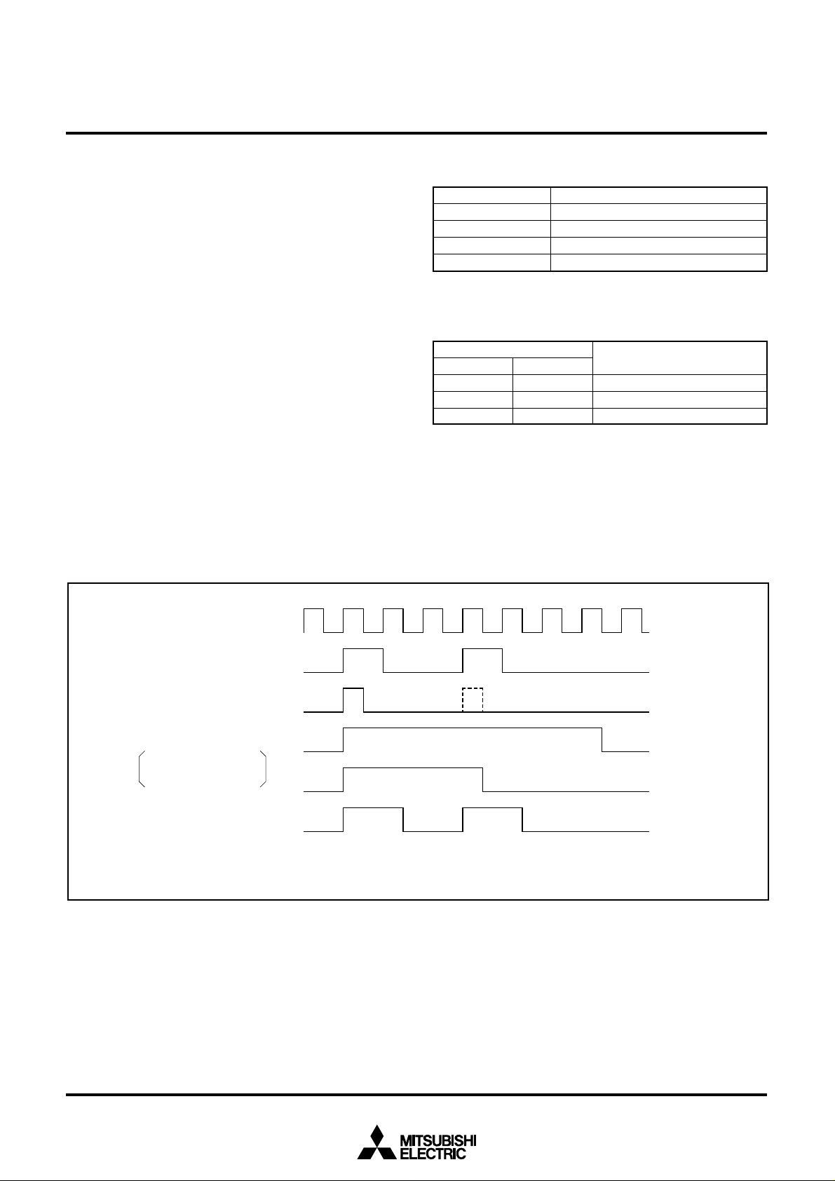
● Number of bus cycles
Figure 9 shows the bus cycle waveform at access to the internal
area. Bit 7 of the processor mode register 1 (address 5F16), which is
shown in Figure 10, selects the number of bus cycles for the internal
1 bus cycle = 3φ (Note)
(Internal ROM bus cycle select bit = 0)
1 bus cycle = 3φ
BIU
φ
ROM
RAM
SFR
Internal address bus
Internal data bus,
Internal code bus
Address
Internal address bus
Internal data bus,
Internal code bus
Data
φ
BIU
ROM: 3φ or 2φ. (This bit 7 is the internal ROM bus cycle select bit.)
The internal RAM, SFRs (internal peripheral devices’ control registers) are always accessed with 1 bus cycle = 2φ.
1 bus cycle = 2φ
(Internal ROM bus cycle select bit = 1)
1 bus cycle = 2φ
φ
BIU
Internal address bus
Internal data bus
Internal code bus
1 bus cycle = 2φ
Address
Data
Address
Data
Note: When reprogramming the internal flash memory in the CPU reprogramming mode, select the bus cycle = 3φ.
Fig. 9 Bus cycle waveform at access to internal area
76543210
0000000
Fig. 10 Bit configuration of processor mode register 1
Processor mode register 1
Fix these bits to “0000000
Internal ROM bus cycle select bit
0 : 1 bus cycle = 3φ
1 : 1 bus cycle = 2φ
2
”.
Address
16
5F
19
Page 20
M37905M4C-XXXFP, M37905M4C-XXXSP
M37905M6C-XXXFP, M37905M6C-XXXSP
PRELIMINARY
Notice: This is not a final specification.
Some parametric limits are subject to change.
PROCESSOR MODES
This microcomputer is dedicated to the single-chip mode. Therefore,
be sure to connect pin MD0 to Vss, and be sure to fix the processor
mode bits (bits 1 and 0 of the processor mode register 0, address
5E16), which is shown in Figure 11, to “002”.
M37905M8C-XXXFP, M37905M8C-XXXSP
MITSUBISHI MICROCOMPUTERS
16-BIT CMOS MICROCOMPUTER
76543210
0
Fig. 11 Bit configuration of processor mode register 0
00
00
Processor mode register 0
Processor mode bits
0 0 : Single-chip mode
0 1 : Do not select.
1 0 : Do not select.
1 1 : Do not select.
Fix these bits to “00
Interrupt priority detection time select bits
0 0 : 7 cycles of f
0 1 : 4 cycles of f
1 0 : 2 cycles of f
1 1 : Do not select.
Software reset bit
By a write of “1” to this bit, the microcomputer will be reset, and then, restarted.
Fix this bit to “0”.
sys
sys
sys
2
”.
Address
16
5E
20
Page 21
PRELIMINARY
76543210
INT0 read bit
INT
1
read bit
INT
2
read bit
INT
3
read bit
INT
4
read bit
INT
5
read bit
INT
6
read bit
INT
7
read bit
External interrupt input read register
Address
95
16
Notice: This is not a final specification.
Some parametric limits are subject to change.
MITSUBISHI MICROCOMPUTERS
M37905M4C-XXXFP, M37905M4C-XXXSP
M37905M6C-XXXFP, M37905M6C-XXXSP
M37905M8C-XXXFP, M37905M8C-XXXSP
16-BIT CMOS MICROCOMPUTER
INTERRUPTS
Table 3 shows the interrupt sources and the corresponding interrupt
vector addresses. Reset is also handled as an interrupt source in
this section, too.
DBC and BRK instruction are interrupts used only for debugging.
Therefore, do not use these interrupts.
Interrupts other than reset, watchdog timer, zero divide, and address
matching detection all have interrupt control registers. Table 4 shows
the addresses of the interrupt control registers and Figure 13 shows
the bit configuration of the interrupt control register.
The interrupt request bit is automatically cleared by the hardware
during reset or when processing an interrupt. Also, interrupt request
bits except for that of a watchdog timer interrupt can be cleared by
software.
An INTi (i = 0 to 7) interrupt request is generated by an external input.
INTi is an external interrupt; whether to cause an interrupt at the input level (level sense) or at the edge (edge sense) can be selected
with the level/edge select bit. Furthermore, the polarity of the interrupt input can be selected with the polarity select bit.
When using the following pins as external interrupt input pins, be
sure to clear the direction registers of the corresponding multiplexed
ports to “0”: pins P51/INT1, P52/INT2, P53/INT3, P55/INT5, P56/INT6,
and P57/INT7.
When the external interrupt input read register (address 9516), which
is shown in Figure 12, is read out, the status of pins INT0 through
INT7 can directly be read.
Timer and UART interrupts are described in the respective section.
The priority of interrupts when multiple interrupt requests are caused
simultaneously is partially fixed by hardware, but, it can also be adjusted by software as shown in Figure 14.
The hardware priority is fixed as the following:
reset > watchdog timer > other interrupts
Table 3. Interrupt sources and interrupt vector addresses
Interrupts
UART2 transmit
UART2 receive
Timer A9
Timer A8
Timer A7
Timer A6
Timer A5
INT7 external interrupt
INT6 external interrupt
INT5 external interrupt
Address matching detection interrupt
INT4 external interrupt
INT3 external interrupt
A-D conversion
UART1 transmit
UART1 receive
UART0 transmit
UART0 receive
Timer B2
Timer B1
Timer B0
Timer A4
Timer A3
Timer A2
Timer A1
Timer A0
INT2 external interrupt
INT1 external interrupt
INT0 external interrupt
Watchdog timer
DBC (Do not select.)
Break instruction (Do not select.)
Zero divide
Reset
Vector addresses
00FFB416 00FFB516
00FFB616 00FFB716
00FFB816 00FFB916
00FFBA16 00FFBB16
00FFBC16 00FFBD16
00FFBE16 00FFBF16
00FFC016 00FFC116
00FFC216 00FFC316
00FFC416 00FFC516
00FFC616 00FFC716
00FFCA16 00FFCB16
00FFD016 00FFD116
00FFD216 00FFD316
00FFD416 00FFD516
00FFD616 00FFD716
00FFD816 00FFD916
00FFDA16 00FFDB16
00FFDC16 00FFDD16
00FFDE16 00FFDF16
00FFE016 00FFE116
00FFE216 00FFE316
00FFE416 00FFE516
00FFE616 00FFE716
00FFE816 00FFE916
00FFEA16 00FFEB16
00FFEC16 00FFED16
00FFEE16 00FFEF16
00FFF016 00FFF116
00FFF216 00FFF316
00FFF616 00FFF716
00FFF816 00FFF916
00FFFA16 00FFFB16
00FFFC16 00FFFD16
00FFFE16 00FFFF16
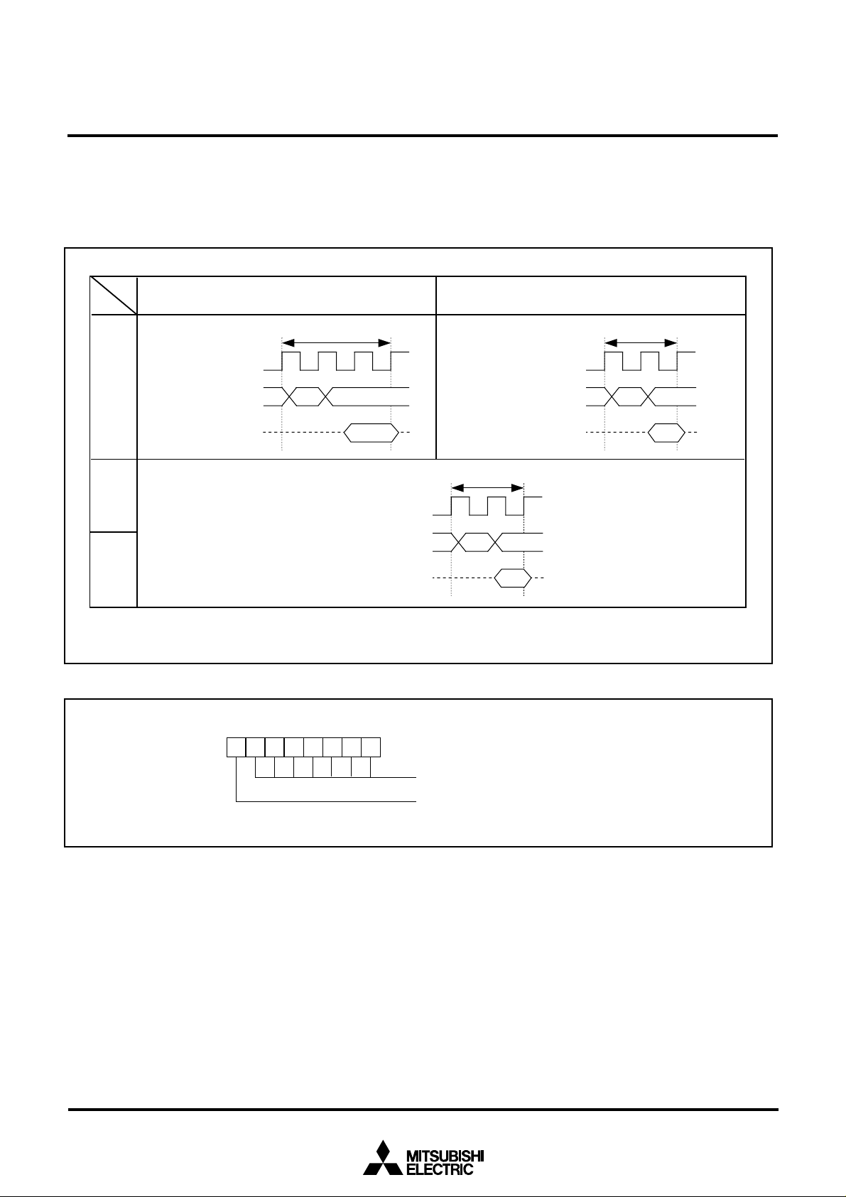
Fig. 12 Bit configuration of external interrupt input read register
21
Page 22
PRELIMINARY
Notice: This is not a final specification.
Some parametric limits are subject to change.
76543210
Interrupt control register bit configuration for A-D converter, UART0, UART1, UART2,
timer A0 to timer A9, and timer B0 to timer B2.
76543210
MITSUBISHI MICROCOMPUTERS
M37905M4C-XXXFP, M37905M4C-XXXSP
M37905M6C-XXXFP, M37905M6C-XXXSP
M37905M8C-XXXFP, M37905M8C-XXXSP
16-BIT CMOS MICROCOMPUTER
Interrupt priority level select bits (Note 1)
Interrupt request bit
0 : No interrupt requested
1 : Interrupt requested
Interrupt priority level select bits (Note 1)
Interrupt request bit (Note 2)
0 : No interrupt requested
1 : Interrupt requested
Polarity select bit
0 : Interrupt request bit is set to “1” at “H” level when level sense is selected;
this bit is set to “1” at falling edge when edge sense is selected.
1 : Interrupt request bit is set to “1” at “L” level when level sense is selected;
this bit is set to “1” at rising edge when edge sense is selected.
Level/Edge select bit
0 : Edge sense
1 : Level sense
Interrupt control register bit configuration for INT
Notes 1: Use the MOVM (MOVMB) instruction or the STA (STAB, STAD) instruction for writing to this bit.
2: Interrupt request bits of INT
Fig. 13 Bit configuration of interrupt control register
0
– INT
7
0
to INT7 are invalid when the level sense is selected.
22
Page 23
PRELIMINARY
Notice: This is not a final specification.
Some parametric limits are subject to change.
MITSUBISHI MICROCOMPUTERS
M37905M4C-XXXFP, M37905M4C-XXXSP
M37905M6C-XXXFP, M37905M6C-XXXSP
M37905M8C-XXXFP, M37905M8C-XXXSP
16-BIT CMOS MICROCOMPUTER
Table 4. Addresses of interrupt control registers
Interrupt control registers
INT3 interrupt control register
INT4 interrupt control register
A-D interrupt control register
UART0 transmit interrupt control register
UART0 receive interrupt control register
UART1 transmit interrupt control register
UART1 receive interrupt control register
Timer A0 interrupt control register
Timer A1 interrupt control register
Timer A2 interrupt control register
Timer A3 interrupt control register
Timer A4 interrupt control register
Timer B0 interrupt control register
Timer B1 interrupt control register
Timer B2 interrupt control register
INT0 interrupt control register
INT1 interrupt control register
INT2 interrupt control register
UART2 transmit interrupt control register
UART2 receive interrupt control register
Timer A5 interrupt control register
Timer A6 interrupt control register
Timer A7 receive control register
Timer A8 interrupt control register
Timer A9 interrupt control register
INT5 interrupt control register
INT6 interrupt control register
INT7 interrupt control register
Addresses
00006E16
00006F16
00007016
00007116
00007216
00007316
00007416
00007516
00007616
00007716
00007816
00007916
00007A16
00007B16
00007C16
00007D16
00007E16
00007F16
0000F116
0000F216
0000F516
0000F616
0000F716
0000F816
0000F916
0000FD16
0000FE16
0000FF16
Interrupts caused by the address matching detection and when dividing by zero are software interrupts and are not included in Figure
14.
Other interrupts previously mentioned are A-D converter, UART , etc.
interrupts. The priority of these interrupts can be changed by changing the priority level in the corresponding interrupt control register by
software.
Figure 15 shows a diagram of the interrupt priority detection circuit.
When an interrupt is caused, each interrupt device compares its own
priority with the priority from above and if its own priority is higher,
then it sends the priority below and requests the interrupt. If the priorities are the same, the one above has priority.
This comparison is repeated to select the interrupt with the highest
priority among the interrupts that are being requested. Finally the
selected interrupt is compared with the processor interrupt priority
level (IPL) contained in the processor status register (PS) and the
request is accepted if it is higher than IPL and the interrupt disable
flag I is “0”. The request is not accepted if flag I is “1”. The reset and
watchdog timer interrupts are not affected by the interrupt disable
flag I.
When an interrupt is accepted, the contents of the processor status
register (PS) is saved to the stack and the interrupt disable flag I is
set to “1”.
Furthermore, the interrupt request bit of the accepted interrupt is
cleared to “0” and the processor interrupt priority level (IPL) in the
A-D converter, UART, etc. interrupts
Priority can be changed by software inside ➂.
Fig. 14 Interrupt priority
Interrupt request
Reset
Watchdog timer
Interrupt disable flag I
IPL
Fig. 15 Interrupt priority detection
Priority is determined by hardware
➂➁➀
Watchdog
UART2 transmit
UART2 receive
Timer A9
Timer A8
Timer A7
Timer A6
Timer A5
INT7
INT6
INT5
INT4
INT
3
A-D
UART1 transmit
UART1 receive
UART0 transmit
UART0 receive
Timer B2
Timer B1
Timer B0
Timer A4
Timer A3
Timer A2
Timer A1
Timer A0
INT2
INT1
INT0
timer
Reset
Level 0
23
Page 24
PRELIMINARY
Notice: This is not a final specification.
Some parametric limits are subject to change.
MITSUBISHI MICROCOMPUTERS
M37905M4C-XXXFP, M37905M4C-XXXSP
M37905M6C-XXXFP, M37905M6C-XXXSP
M37905M8C-XXXFP, M37905M8C-XXXSP
16-BIT CMOS MICROCOMPUTER
processor status register (PS) is replaced by the priority level of the
accepted interrupt.
Therefore, multi-level priority interrupts are possible by resetting the
interrupt disable flag I to “0” and enable further interrupts.
For reset, watchdog timer, zero divide, and address match detection
interrupts, which do not have an interrupt control register, the processor interrupt level (IPL) is set as shown in Table 5.
The interrupt request bit and the interrupt priority level of each interrupt source are sampled and latched at each operation code fetch
cycle while fsys is “H”. However, no sampling pulse is generated until
the cycles whose number is selected by software has passed, even
if the next operation code fetch cycle is generated. The detection of
an interrupt which has the highest priority is performed during that
time.
As shown in Figure 16, there are three different interrupt priority detection time from which one is selected by software. After the selected time has elapsed, the highest priority is determined and is
processed after the currently executing instruction has been completed.
The time is selected with bits 4 and 5 of the processor mode register
0 (address 5E16) shown in Figure 11. Table 6 shows the relationship
between these bits and the number of cycles. After a reset, the processor mode register 0 is initialized to “0016.” Therefore, the longest
time is automatically set, however, the shortest time must be selected by software.
Table 5.
Value loaded in processor interrupt level (IPL) during an interrupt
Interrupt types
Reset
Watchdog timer
Zero divide
Address matching detection
Setting value
0
7
Not change value of IPL.
Not change value of IPL.
Table 6. Relationship between interrupt priority detection time select
bit and number of cycles
Priority detection time select bit
Bit 5
0
0
1
Bit 4
0
1
0
Number of cycles (Note)
7 cycles of fsys
4 cycles of fsys
2 cycles of fsys
Note: For system clock fsys, refer to the section on the clock gener-
ating circuit.
f
sys
Operation code fetch cycle
Sampling pulse
Priority detection time
Select one between 00 to
10 with bits 4 and 5 of
processor mode register 0
Fig. 16 Interrupt priority detection time
(Note)
b5 b4
0 0
0 1
1 0
sys
Note: This pulse resides when 2 cycles of f
is selected.
24
Page 25
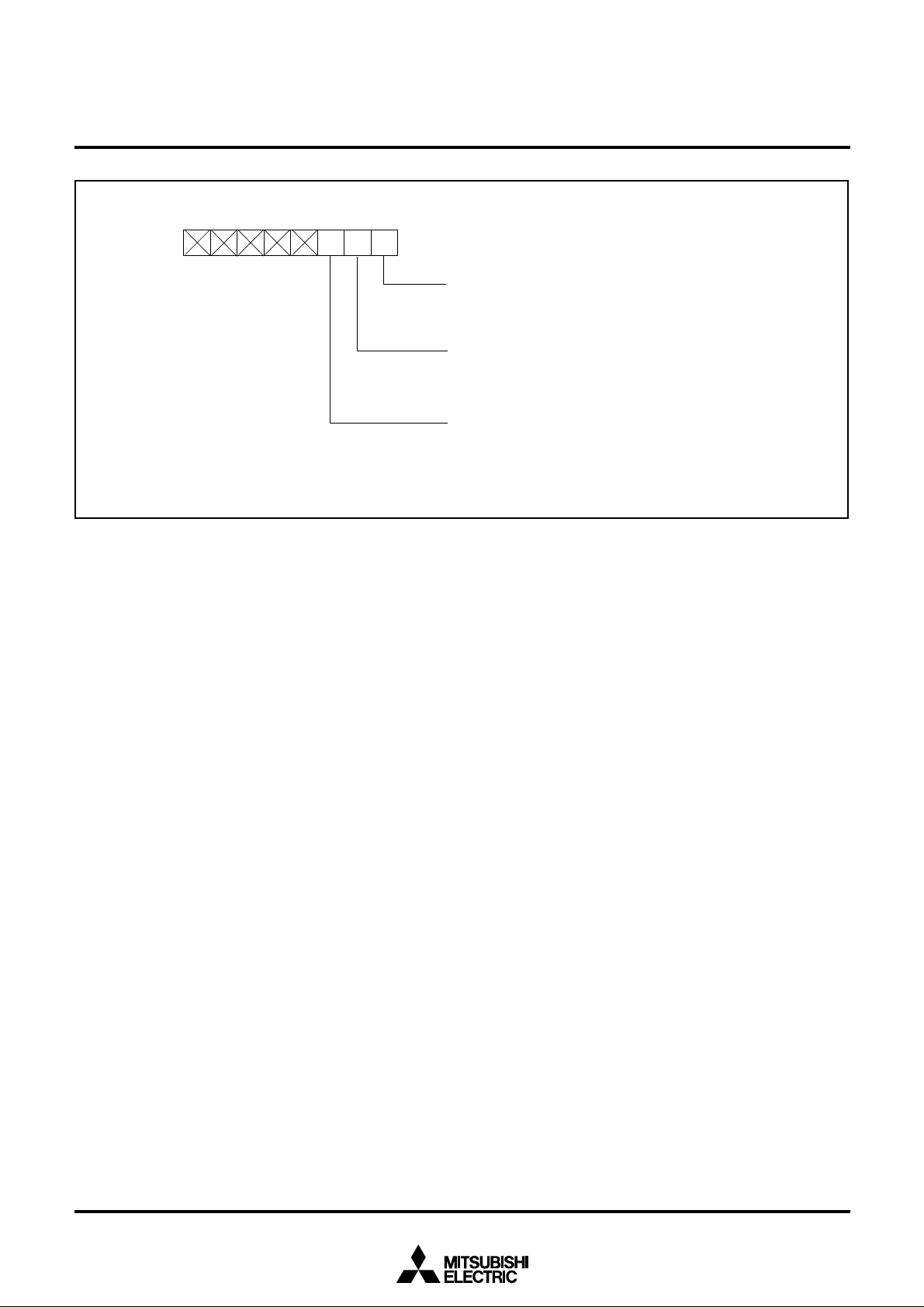
PRELIMINARY
Notice: This is not a final specification.
Some parametric limits are subject to change.
MITSUBISHI MICROCOMPUTERS
M37905M4C-XXXFP, M37905M4C-XXXSP
M37905M6C-XXXFP, M37905M6C-XXXSP
M37905M8C-XXXFP, M37905M8C-XXXSP
16-BIT CMOS MICROCOMPUTER
76543210
Fig. 17 Bit configuration of port P2 pin function control register
Port P2 pin function control register
Pin TB0
0: Allocate pin TB0
1: Allocate pin TB0
Pin TB1IN select bit
0: Allocate pin TB1
1: Allocate pin TB1
Pin TB2
0: Allocate pin TB2
1: Allocate pin TB2
IN
select bit
IN
select bit
IN
to P55.
IN
to P24.
IN
to P56.
IN
to P25.
IN
to P57.
IN
to P26.
Address
16
AE
25
Page 26
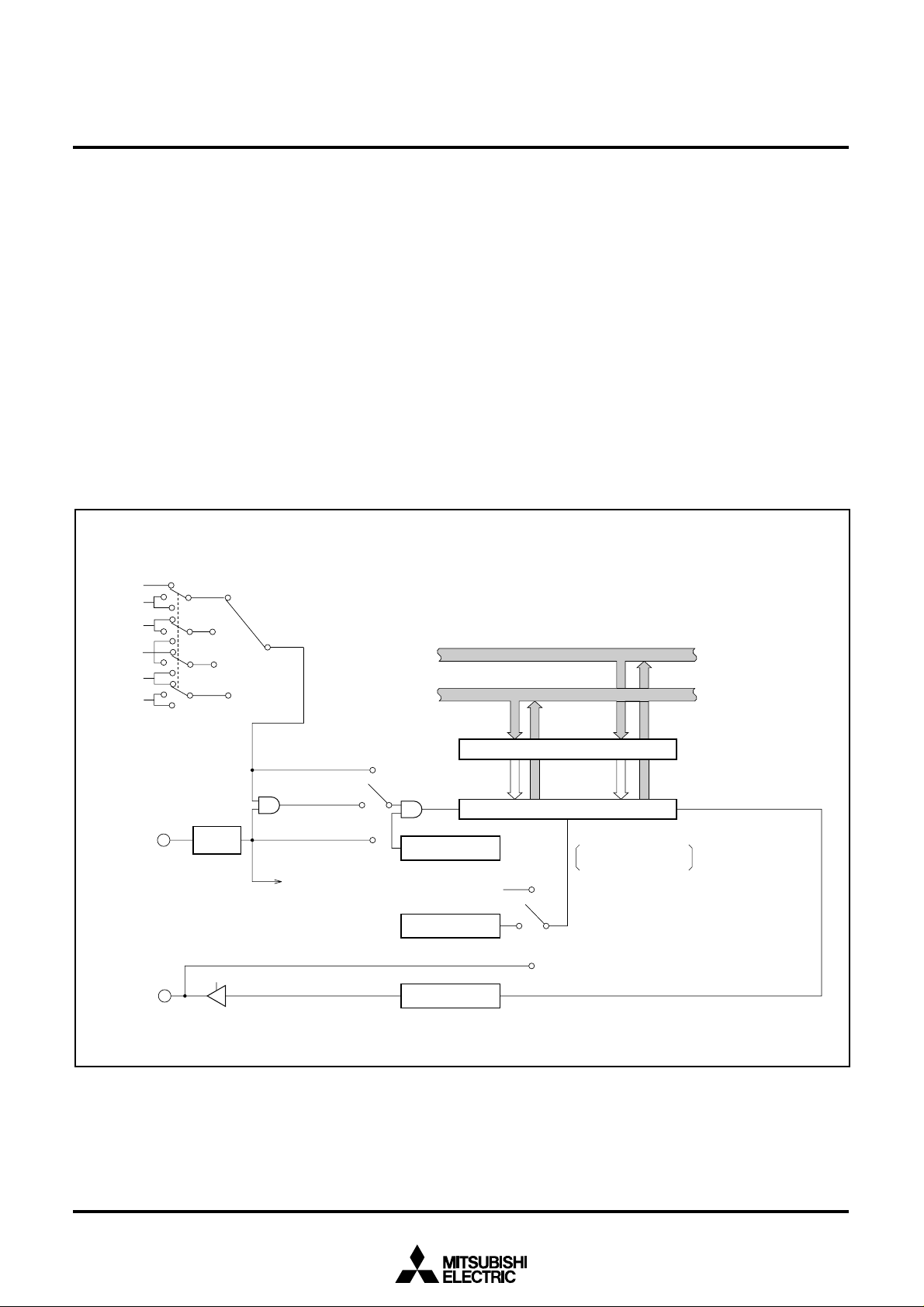
PRELIMINARY
Notice: This is not a final specification.
Some parametric limits are subject to change.
MITSUBISHI MICROCOMPUTERS
M37905M4C-XXXFP, M37905M4C-XXXSP
M37905M6C-XXXFP, M37905M6C-XXXSP
M37905M8C-XXXFP, M37905M8C-XXXSP
16-BIT CMOS MICROCOMPUTER
TIMER
There are eight 16-bit timers. They are divided by type into timer A
(10) and timer B (3).
The timer I/O pins are multiplexed with I/O pins for ports P2, P4, P5
and P6. To use these pins as timer input pins, the port direction register bit corresponding to the pin must be cleared to “0” to specify
input mode.
TIMER A
Figure 18 shows a block diagram of timer A.
Timer A has four modes: timer mode, event counter mode, one-shot
pulse mode, and pulse width modulation mode. The mode is selected with bits 0 and 1 of the timer Ai mode register (i = 0 to 9). Each
of these modes is described below.
Figure 19 shows the bit configuration of the timer A clock division select register. Timers A0 to A9 use the count source which has been
selected by bits 0 and 1 of this register.
Timer A clock
division select bit
f
2
f
1
f
16
Count source
select bits
(1) Timer mode [00]
Figure 20 shows the bit configuration of the timer Ai mode register in
the timer mode. Bits 0, 1 and 5 of the timer Ai mode register must be
“0” in timer mode. The timer A’s count source is selected by bits 6
and 7 of the timer Ai mode register and the contents of the timer A
clock division select register. (See Table 7.)
The counting of the selected clock starts when the count start bit is
“1” and stops when it is “0”.
Figure 21 shows the bit configuration of the count start bit. The
counter is decremented, an interrupt is caused and the interrupt request bit in the timer Ai interrupt control register is set when the contents becomes 000016. At the same time, the contents of the reload
register is transferred to the counter and count is continued.
f
64
f
512
f
4096
Polarity
selection
IN
TAi
(i = 0–9)
Pulse output
TAi
OUT
(i = 0–9)
Fig. 18 Block diagram of timer A
• Timer
• One-shot pulse
• Pulse width
Timer (gate function)
Event counter
External trigger
Count start registers 0, 1
(Addresses 4016, 4116)
Countdown
Up-down registers 0, 1
(Addresses 4416, C416)
Toggle flip-flop
Data bus (odd)
Data bus (even)
(Low-order 8 bits) (High-order 8 bits)
Reload register(16)
Counter (16)
Countup/Countdown switching
“Countdown” is always
selected when not in the
event counter mode.
Timer A0 4716 46
Timer A1 4916 48
Timer A2 4B16 4A
Timer A3 4D16 4C
Timer A4 4F16 4E
Addresses
16
16
16
16
16
Timer A5 C716 C6
Addresses
Timer A6 C916 C8
Timer A7 CB16 CA
Timer A8 CD16 CC
Timer A9 CF16 CE
16
16
16
16
16
26
Page 27
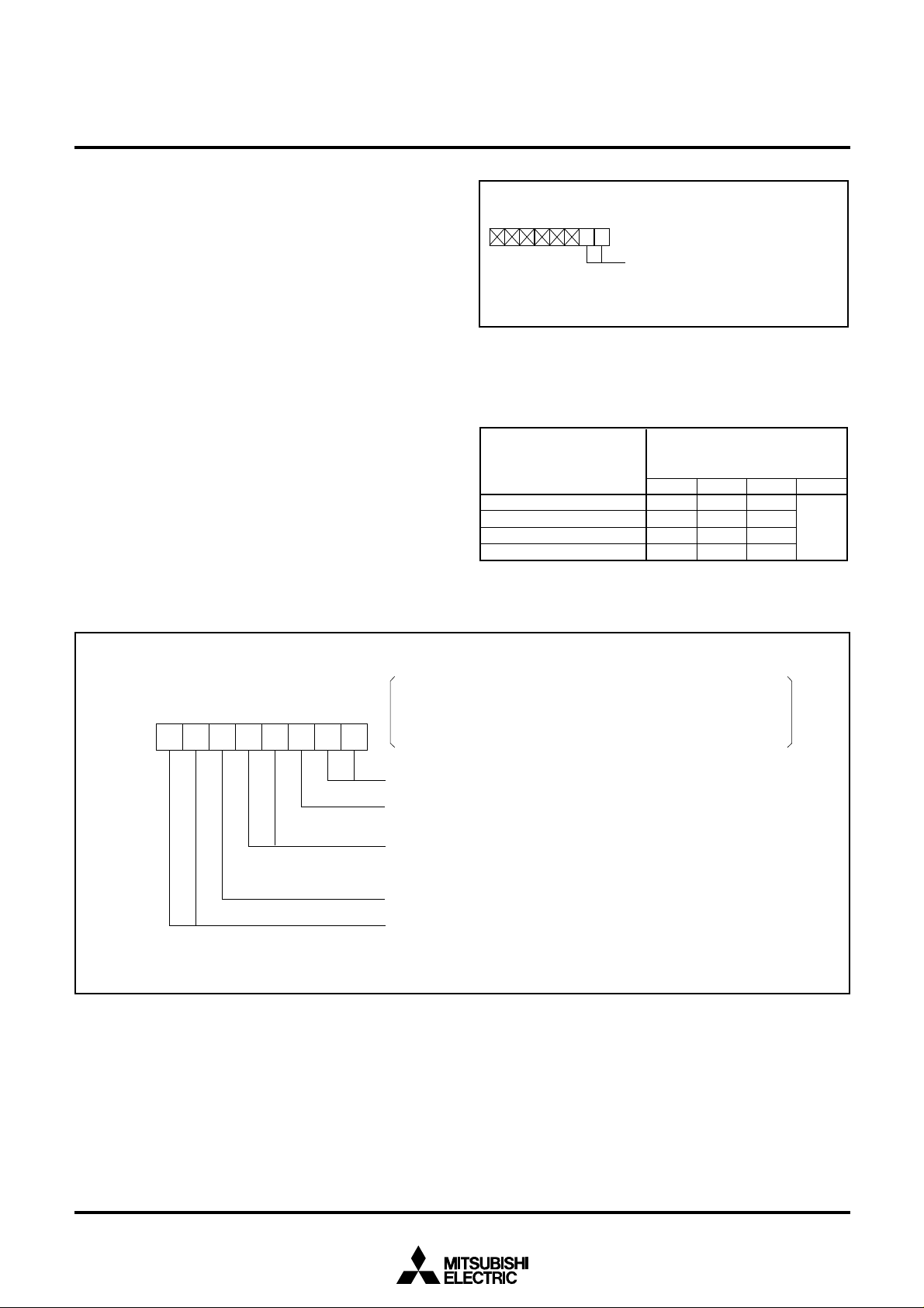
M37905M4C-XXXFP, M37905M4C-XXXSP
Clock source select bits
(bits 7 and 6 at addresses
56
16
to 5A16)
(bits 7 and 6 at addresses
D6
16
to DA16)
1 0
0 0
0 1
Timer A clock division select bits
(bits 1 and 0 at address 45
16
)
f
2
f
16
f
64
1 1 f
512
00
f
1
f
16
f
64
f
4096
01
f
1
f
64
f
512
f
4096
10
11
Do not
select.
Note: Timers A0 to A9 use the same clock, which is selected by the
timer A clock division select bits.
M37905M6C-XXXFP, M37905M6C-XXXSP
PRELIMINARY
Notice: This is not a final specification.
Some parametric limits are subject to change.
When bit 2 of the timer Ai mode register is “1”, the output is generated from TAiOUT pin. The output is toggled each time the contents
of the counter reaches to 000016. When the contents of the count
start bit is “0”, “L” is output from TAiOUT pin.
When bit 2 is “0”, TAiOUT can be used as a normal port pin. When bit
4 is “0”, TAiIN can be used as a normal port pin.
When bit 4 is “1”, counting is performed only while the input signal
from the T AiIN pin is “H” or “L” as shown in Figure 22. Therefore, this
can be used to measure the pulse width of the TAiIN input signal.
Whether to count while the input signal is “H” or while it is “L” is determined by bit 3. If bit 3 is “1”, counting is performed while the TAiIN
pin input signal is “H” and if bit 3 is “0”, counting is performed while it
is “L”.
Note that, the duration of “H” or “L” on the TAiIN pin must be 2 or
more cycles of the timer count source.
When data is written to timer Ai register with timer Ai halted, the
same data is also written to the reload register and the counter.
When data is written to timer Ai which is busy, the data is written to
the reload register, but not to the counter. The new data is reloaded
from the reload register to the counter at the next reload time and
counting continues. The contents of the counter can be read at any
time.
When the value set in the timer Ai register is n, the timer frequency
division ratio is 1/(n+1).
M37905M8C-XXXFP, M37905M8C-XXXSP
MITSUBISHI MICROCOMPUTERS
16-BIT CMOS MICROCOMPUTER
76543210
Timer A clock division select register
Timer A clock division select bit
(See Table 7.)
Fig. 19 Bit configuration of timer A clock division select register
Table 7. Relationship between timer A clock division select bits,
clock source select bits, and count source
Address
45
16
Timer A0 mode register
Timer A1 mode register
6543210
7
0
00
Timer A2 mode register
Timer A3 mode register
Timer A4 mode register
0 0 : Always “00” in timer mode
0 : No pulse output (TAi
1 : Pulse output (TAi
×
: No gate function (TAiIN is normal port pin.)
0
1 0 : Count only while TAi
1 1 : Count only while TAi
0 : Always “0” in timer mode.
Clock source select bits
See Table 7.
Fig. 20 Bit configuration of timer Ai mode register in timer mode
Addresses
56
16
5716
5816
5916
5A16
OUT is normal port pin.)
OUT is pulse output pin.)
IN input is “L”.
IN input is “H”.
Timer A5 mode register
Timer A6 mode register
Timer A7 mode register
Timer A8 mode register
Timer A9 mode register
Addresses
16
D6
D716
D816
D916
DA16
27
Page 28
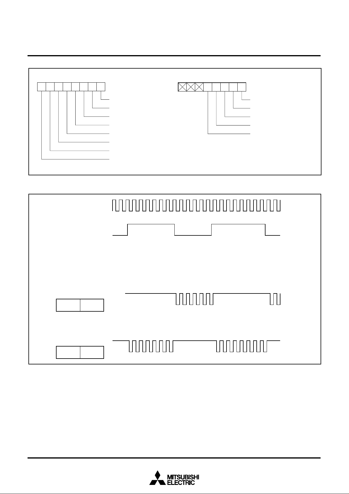
PRELIMINARY
Notice: This is not a final specification.
Some parametric limits are subject to change.
MITSUBISHI MICROCOMPUTERS
M37905M4C-XXXFP, M37905M4C-XXXSP
M37905M6C-XXXFP, M37905M6C-XXXSP
M37905M8C-XXXFP, M37905M8C-XXXSP
16-BIT CMOS MICROCOMPUTER
76543210
Count start register 0
(Stopped at “0”, Started at “1”)
Timer A0 count start bit
Timer A1 count start bit
Timer A2 count start bit
Timer A3 count start bit
Timer A4 count start bit
Timer B0 count start bit
Timer B1 count start bit
Timer B2 count start bit
Fig. 21 Bit configuration of count start register
Selected clock source fi
TAi
IN
Address
16
40
76543210
Count start register 1
(Stopped at “0”, Started at “1”)
Timer A5 count start bit
Timer A6 count start bit
Timer A7 count start bit
Timer A8 count start bit
Timer A9 count start bit
Address
16
41
Timer mode register
Bit 4 Bit 3
10
Timer mode register
Bit 4 Bit 3
11
Fig. 22 Count waveform when gate function is available
28
Page 29
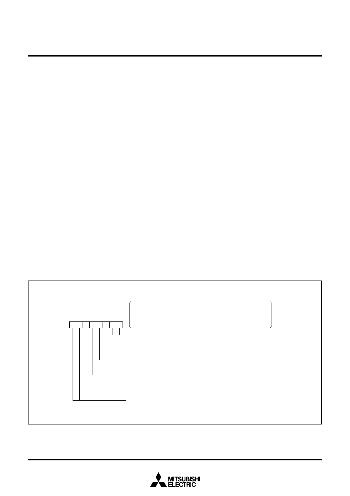
PRELIMINARY
Notice: This is not a final specification.
Some parametric limits are subject to change.
MITSUBISHI MICROCOMPUTERS
M37905M4C-XXXFP, M37905M4C-XXXSP
M37905M6C-XXXFP, M37905M6C-XXXSP
M37905M8C-XXXFP, M37905M8C-XXXSP
16-BIT CMOS MICROCOMPUTER
(2) Event counter mode [01]
Figure 23 shows the bit configuration of the timer Ai mode register in
the event counter mode. In event counter mode, bit 0 of the timer Ai
mode register must be “1” and bits 1 and 5 must be “0”.
The input signal from the TAiIN pin is counted when the count start
bit shown in Figure 21 is “1” and counting is stopped when it is “0”.
Count is performed at the fall of the input signal when bit 3 is “0” and
at the rise of the signal when it is “1”.
In event counter mode, whether to increment or decrement the count
can be selected with the up-down bit or the input signal from the
TAiOUT pin.
When bit 4 of the timer Ai mode register is “0”, the up-down bit is
used to determine whether to increment or decrement the count
(decrement when the bit is “0” and increment when it is “1”). Figure
24 shows the bit configuration of the up-down register.
When bit 4 of the timer Ai mode register is “1”, the input signal from
the TAiOUT pin is used to determine whether to increment or decrement the count. However, note that bit 2 must be “0” if bit 4 is “1”. It is
because if bit 2 is “1”, TAiOUT pin becomes an output pin to output
pulses.
The count is decremented when the input signal from the T AiOUT pin
is “L” and incremented when it is “H”. Determine the level of the input
signal from the TAiOUT pin before a valid edge is input to the TAiIN
pin.
An interrupt request signal is generated and the interrupt request bit
in the timer Ai interrupt control register is set when the counter
reaches 000016 (decrement count) or FFFF16 (increment count). At
the same time, the contents of the reload register is transferred to the
counter and the count is continued.
When bit 2 is “1”, each time the counter reaches 000016 (decrement
count) or FFFF16 (increment count), the waveform’s polarity is reversed and is output from TAiOUT pin.
If bit 2 is “0”, TAiOUT pin can be used as a normal port pin.
However, if bit 4 is “1” and the TAiOUT pin is used as an output pin,
the output from the pin changes the count direction. Therefore, bit 4
must be “0” unless the output from the T AiOUT pin is to be used to select the count direction.
Data write and data read are performed in the same way as for timer
mode. That is, when data is written to timer Ai halted, it is also written to the reload register and the counter. When data is written to
timer Ai which is busy, the data is written to the reload register, but
not to the counter. The counter is reloaded with new data from the
reload register at the next reload time. The counter can be read at
any time.
In event counter mode, whether to increment or decrement the
counter can also be determined by supplying two kinds of pulses of
which phases differ by 90° to timer A2, A3, A4, A7, A8 or A9. There
are two types of two-phase pulse processing operations. One uses
timers A2, A3, A7, and A8 and the other uses timers A4 and A9. In
both processing operations, two pulses described above are input to
the TAjOUT (j = 2 to 4, 7 to 9) pin and TAjIN pin respectively.
When timers A2, A3, A7, and A8 are used, as shown in Figure 25, the
count is incremented when a rising edge is input to the TAkIN (k=2,
3, 7, 8) pin after the level of T AkOUT pin changes from “L” to “H”, and
when the falling edge is input, the count is decremented.
For timers A4 and A9, as shown in Figure 26, when a phase-related
pulse with a rising edge input to the TAlIN (l = 4, 9) pin is input after
the level of TAlOUT pin changes from “L” to “H”, the count is
incremented at the respective rising edge and falling edge of the
TAlOUT pin and TAlIN pin.
Timer A0 mode register
Timer A1 mode register
76543210
××
0
Timer A2 mode register
Timer A3 mode register
Timer A4 mode register
10
0 1 : Always “01” in event counter mode
0 : No pulse output
1 : Pulse output
0 : Count at the falling edge of input signal
1 : Count at the rising edge of input signal
0 : Increment or decrement according to up/down bit
1 : Increment or decrement according to TAi
0 : Always “0” in event counter mode
× × : Not used in event counter mode
Fig. 23 Bit configuration of timer Ai mode register in event counter mode
Addresses
16
56
5716
5816
5916
5A16
Timer A5 mode register
Timer A6 mode register
Timer A7 mode register
Timer A8 mode register
Timer A9 mode register
OUT pin input signal level
Addresses
16
D6
D716
D816
D916
DA16
29
Page 30
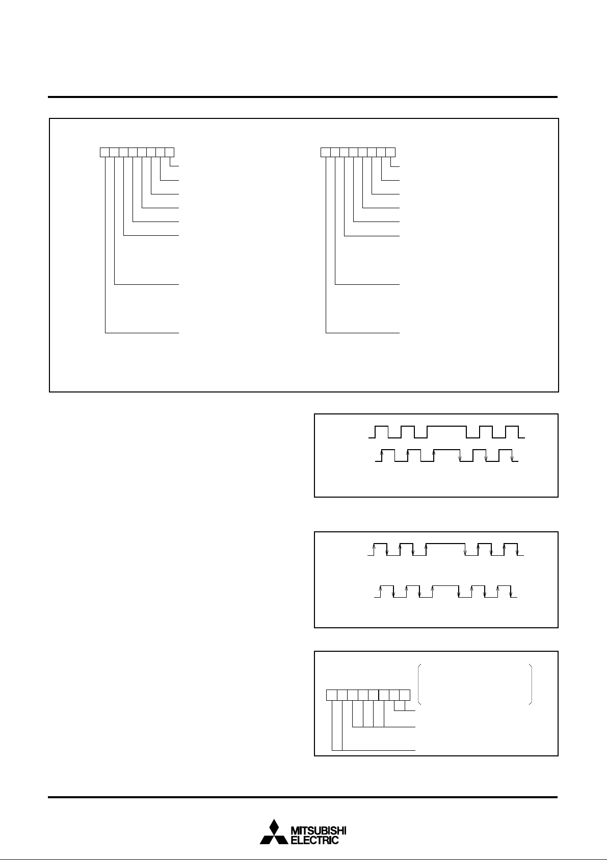
PRELIMINARY
Notice: This is not a final specification.
Some parametric limits are subject to change.
MITSUBISHI MICROCOMPUTERS
M37905M4C-XXXFP, M37905M4C-XXXSP
M37905M6C-XXXFP, M37905M6C-XXXSP
M37905M8C-XXXFP, M37905M8C-XXXSP
16-BIT CMOS MICROCOMPUTER
76543210
Up-down register 0
Timer A0 up-down bit
Timer A1 up-down bit
Timer A2 up-down bit
Timer A3 up-down bit
Timer A4 up-down bit
Timer A2 two-phase pulse signal
processing select bit
0 : Two-phase pulse signal processing
disabled
1 : Two-phase pulse signal processing
mode
Timer A3 two-phase pulse signal
processing select bit
0 : Two-phase pulse signal processing
disabled
1 : Two-phase pulse signal processing
mode
Timer A4 two-phase pulse signal
processing select bit
0 : Two-phase pulse signal processing
disabled
1 : Two-phase pulse signal processing
mode
Address
16
44
Fig. 24 Bit configuration of up-down register
When a phase-related pulse with a falling edge input to the TAkOUT
pin is input after the level of TAlIN pin changes from “H” to “L”, the
count is decremented at the respective rising edge and falling edge
of the TAlIN pin and TAlOUT pin. When performing this two-phase
pulse signal processing, bits 0 and 4 of timer Aj mode register must
be set to “1” and bits 1, 2, 3, and 5 must be “0”. Bits 6 and 7 are ignored. (See Figure 27.) Note that bits 5, 6, and 7 of the up-down register 0 (address 4416) are the two-phase pulse signal processing
select bits for timers A2, A3, and A4, respectively . Also, bits 5, 6, and
7 of the up-down register 1 (address C416) are the two-phase pulse
signal processing select bits for timers A7, A8, and A9, respectively.
Each timer operates in normal event counter mode when the corresponding bit is “0” and performs two-phase pulse signal processing
when it is “1”.
Count is started by setting the count start bit to “1”. Data write and
read are performed in the same way as for normal event counter
mode. Note that the direction register of the input port must be set to
input mode because two kinds of pulse signals, described above,
are input. Also, there can be no pulse output in this mode.
76543210
TAk
OUT
TAk
IN
(k = 2, 3, 7, 8)
Incrementcount
Up-down register 1
Timer A5 up-down bit
Timer A6 up-down bit
Timer A7 up-down bit
Timer A8 up-down bit
Timer A9 up-down bit
Timer A7 two-phase pulse signal
processing select bit
0 : Two-phase pulse signal processing
disabled
1 : Two-phase pulse signal processing
mode
Timer A8 two-phase pulse signal
processing select bit
0 : Two-phase pulse signal processing
disabled
1 : Two-phase pulse signal processing
mode
Timer A9 two-phase pulse signal
processing select bit
0 : Two-phase pulse signal processing
disabled
1 : Two-phase pulse signal processing
mode
Incre-
Incre-
ment-
ment-
count
count
Decrementcount
Address
16
C4
Decrementcount
Decrementcount
Fig. 25 Two-phase pulse processing operation of timer A2, A3, A7,
A8
TAl
OUT
TAl
IN
(l = 4, 9)
Increment-count at each edge
Decrement-count at each edge
Decrement-count at each edgeIncrement-count at each edge
Fig. 26 Two-phase pulse processing operation of timers A4 and A9
30
Addresses
58
76543210
××
0100
10
Timer A2 mode register
Timer A3 mode register
Timer A4 mode register
Timer A7 mode register
Timer A8 mode register
Timer A9 mode register
0 1 : Always “01” in event counter mode
0 1 0 0 : Always “0100” when processing
two-phase pulse signal
× × : Not used in event counter mode
5A
C8
C9
CA
16
59
16
16
16
16
16
Fig. 27 Bit configuration of timer Aj mode register when performing
two-phase pulse signal processing in event counter mode
Page 31

PRELIMINARY
Notice: This is not a final specification.
Some parametric limits are subject to change.
MITSUBISHI MICROCOMPUTERS
M37905M4C-XXXFP, M37905M4C-XXXSP
M37905M6C-XXXFP, M37905M6C-XXXSP
M37905M8C-XXXFP, M37905M8C-XXXSP
16-BIT CMOS MICROCOMPUTER
(3) One-shot pulse mode [10]
Figure 28 shows the bit configuration of the timer Ai mode register in
the one-shot pulse mode. In one-shot pulse mode, bit 0 and bit 5
must be “0” and bit 1 and bit 2 must be “1”.
The trigger is enabled when the count start bit is “1”. The trigger can
be generated by software or it can be input from the TAiIN pin. Software trigger is selected when bit 4 is “0” and the input signal from the
TAiIN pin is used as the trigger when it is “1“.
Bit 3 is used to determine whether to trigger at the fall of the trigger
signal or at the rise. The trigger is at the fall of the trigger signal when
bit 3 is “0” and at the rise of the trigger signal when it is “1”.
Software trigger is generated by setting “1” to a bit in the one-shot
start register. Each bit corresponds to each timer.
Figure 29 shows the bit configuration of the one-shot start register.
As shown in Figure 30, when a trigger signal is received, the counter
counts the clock selected by bits 6 and 7 and the contents of the
timer A clock division select register. (Set Table 7.)
If the contents of the counter is not 000016, the TAiOUT pin goes “H”
when a trigger signal is received. The count direction is decrement.
When the counter reaches 000116, the TAiOUT pin goes “L” and
count is stopped. The contents of the reload register is transferred to
the counter. At the same time, an interrupt request signal is generated and the interrupt request bit in the timer Ai interrupt control register is set. This is repeated each time a trigger signal is received.
The output pulse width is
1
pulse frequency of the selected clock
× (counter’s value at the time of trigger).
If the count start flag is “0”, T AiOUT goes “L”. Therefore, the value corresponding to the desired pulse width must be written to timer Ai before setting the timer Ai count start bit.
As shown in Figure 31, a trigger signal can be received before the
operation for the previous trigger signal is completed. In this case,
the contents of the reload register is transferred to the counter by the
trigger and then that value is decremented.
Except when retriggering while operating, the contents of the reload
register are not transferred to the counter by triggering.
When retriggering, there must be at least one timer count source
cycle before a new trigger can be issued.
Data write is performed in the same way as for timer mode.
When data is written in timer Ai halted, it is also written to the reload
register and the counter.
When data is written to timer Ai which is busy, the data is written to
the reload register, but not to the counter. The counter is reloaded
with new data from the reload register at the next reload time.
Undefined data is read when timer Ai is read.
Timer A0 mode register
Timer A1 mode register
Timer A2 mode register
76543210
Timer A3 mode register
Timer A4 mode register
0110
1 0 : Always “10” in one-shot pulse mode
1 : Always “1” in one-shot pulse mode
0 × : Software trigger
1 0 : Trigger at the falling edge of TAi
1 1 : Trigger at the rising edge of TAi
0 : Always “0” in one-shot pulse mode
Clock source select bits
(See Table 7.)
Fig. 28 Bit configuration of timer Ai mode register in one-shot pulse mode
Address
16
56
57
16
58
16
59
16
5A
16
Timer A5 mode register
Timer A6 mode register
Timer A7 mode register
Timer A8 mode register
Timer A9 mode register
IN
input
IN
input
Address
16
D6
D7
16
D8
16
D9
16
DA
16
31
Page 32

PRELIMINARY
Notice: This is not a final specification.
Some parametric limits are subject to change.
MITSUBISHI MICROCOMPUTERS
M37905M4C-XXXFP, M37905M4C-XXXSP
M37905M6C-XXXFP, M37905M6C-XXXSP
M37905M8C-XXXFP, M37905M8C-XXXSP
16-BIT CMOS MICROCOMPUTER
76543210
0
One-shot start register 0
Timer A0 one-shot start bit
Timer A1 one-shot start bit
Timer A2 one-shot start bit
Timer A3 one-shot start bit
Timer A4 one-shot start bit
Fix this bit to “0”.
Fig. 29 Bit configuration of one-shot start register
Selected clock
source fi
IN
TAi
(rising edge)
OUT
TAi
Example when the contents of the reload register is 000316
Address
16
42
76543210
0
One-shot start register 1
Timer A5 one-shot start bit
Timer A6 one-shot start bit
Timer A7 one-shot start bit
Timer A8 one-shot start bit
Timer A9 one-shot start bit
Fix this bit to “0”.
Address
16
43
Fig. 30 Pulse output example when external rising edge is selected
Selected clock
source fi
TAi
IN
(rising edge)
TAi
OUT
Example when the contents of the reload register is 000416
Fig. 31 Example when trigger is re-issued during pulse output
32
Page 33

PRELIMINARY
Notice: This is not a final specification.
Some parametric limits are subject to change.
MITSUBISHI MICROCOMPUTERS
M37905M4C-XXXFP, M37905M4C-XXXSP
M37905M6C-XXXFP, M37905M6C-XXXSP
M37905M8C-XXXFP, M37905M8C-XXXSP
16-BIT CMOS MICROCOMPUTER
(4) Pulse width modulation mode [11]
Figure 32 shows the bit configuration of the timer Ai mode register in
the pulse width modulation mode. In pulse width modulation mode,
bits 0, 1, and 2 must be set to “1”.
Bit 5 is used to determine whether to perform 16-bit length pulse
width modulator or 8-bit length pulse width modulator. 16-bit length
pulse width modulator is selected when bit 5 is “0” and 8-bit length
pulse width modulator is selected when it is “1”. The 16-bit length
pulse width modulator is described first.
The pulse width modulator can be started with a software trigger or
with an input signal from a TAiIN pin (external trigger).
The software trigger mode is selected when bit 4 is “0”.
Pulse width modulator is started and a pulse is output from TAiOUT
when the count start bit is set to “1”.
The external trigger mode is selected when bit 4 is “1”.
Pulse width modulation starts when a trigger signal is input from the
TAiIN pin when the count start bit is “1”. Whether to trigger at the fall
or rise of the trigger signal is determined by bit 3. The trigger is at the
fall of the trigger signal when bit 3 is “0” and at the rise when it is “1”.
When data is written to timer Ai with the pulse width modulator
halted, it is written to the reload register and the counter.
Then when the count start bit is set to “1” and a software trigger or
an external trigger is issued to start modulation, the waveform shown
in Figure 33 is output continuously.
Once modulation is started, triggers are not accepted. If the value in
the reload register is m, the duration “H” of pulse is
1
selected clock frequency
and the output pulse period is
1
selected clock frequency
An interrupt request signal is generated and the interrupt request bit
in the timer Ai interrupt control register is set at each fall of the output
pulse.
× m
× (216 – 1).
The width of the output pulse is changed by updating timer data. The
update can be performed at any time. The output pulse width is
changed at the rise of the pulse after data is written to the timer.
The contents of the reload register are transferred to the counter just
before the rise of the next pulse so that the pulse width is changed
from the next output pulse.
Undefined data is read when timer Ai is read.
The 8-bit length pulse width modulator is described next.
The 8-bit length pulse width modulator is selected when the timer Ai
mode register bit 5 is “1”.
The reload register and the counter are both divided into 8-bit
halves.
The low-order 8 bits function as a prescaler and the high-order 8 bits
function as the 8-bit length pulse width modulator. The prescaler
counts the clock selected by bits 6, 7, and the contents of the timer A
clock division select register. (See Table 7.) A pulse is generated
when the counter reaches 000016 as shown in Figure 34. At the
same time, the contents of the reload register is transferred to the
counter and count is continued.
Therefore, if the low-order 8 bits of the reload register are n, the period of the generated pulse is
1
selected clock frequency
× (n + 1).
The high-order 8 bits function as an 8-bit length pulse width modulator using this pulse as input. The operation is the same as for 16-bit
length pulse width modulator except that the length is 8 bits. If the
high-order 8 bits of the reload register are m, the duration “H” of
pulse is
1
selected clock frequency
× (n + 1) × m.
And the output pulse period is
1
selected clock frequency
× (n + 1) × (28 – 1).
Address
16
56
57
16
58
16
59
16
5A
16
76543210
111
Timer A0 mode register
Timer A1 mode register
Timer A2 mode register
Timer A3 mode register
Timer A4 mode register
1 1 : Always “11” in pulse width modulation mode
1 : Always “1” in pulse width modulation mode
0 × : Software trigger
1 0 : Trigger at the falling of TAi
1 1 : Trigger at the rising of TAiIN input
0 : 16-bit pulse width modulator
1 : 8-bit pulse width modulator
Clock source select bits
(See Table 7.)
Fig. 32 Bit configuration of timer Ai mode register in pulse width modulation mode
Timer A5 mode register
Timer A6 mode register
Timer A7 mode register
Timer A8 mode register
Timer A9 mode register
IN
input
Address
16
D6
D7
16
D8
16
D9
16
DA
16
33
Page 34

PRELIMINARY
Notice: This is not a final specification.
Some parametric limits are subject to change.
Selected clock
source fi
IN
TAi
(rising edge)
TAi
OUT
1/fi × (m)
MITSUBISHI MICROCOMPUTERS
M37905M4C-XXXFP, M37905M4C-XXXSP
M37905M6C-XXXFP, M37905M6C-XXXSP
M37905M8C-XXXFP, M37905M8C-XXXSP
16-BIT CMOS MICROCOMPUTER
16
1/fi × (2
This trigger is not accepted
– 1)
Example when the contents of the reload register is 0003
Fig. 33 16-bit length pulse width modulator output pulse example
Selected clock
source fi
IN
TAi
(falling edge)
1/fi × (n + 1)
Prescaler output
(when n = 2)
8-bit length pulse
width modulator
output
(when m = 2)
1/fi × (n + 1) × (2
1/fi × (n + 1) × (m)
16
8
– 1)
Fig. 34 8-bit length pulse width modulator output pulse example
34
Page 35

PRELIMINARY
Notice: This is not a final specification.
Some parametric limits are subject to change.
MITSUBISHI MICROCOMPUTERS
M37905M4C-XXXFP, M37905M4C-XXXSP
M37905M6C-XXXFP, M37905M6C-XXXSP
M37905M8C-XXXFP, M37905M8C-XXXSP
16-BIT CMOS MICROCOMPUTER
TIMER B
Figure 35 shows a block diagram of timer B.
Timer B has three modes: timer mode, event counter mode, and
pulse period measurement/pulse width measurement mode. The
mode is selected with bits 0 and 1 of the timer Bi mode register (i=0
to 2). Each of these modes is described below.
(1) Timer mode [00]
Figure 36 shows the bit configuration of the timer Bi mode register in
the timer mode. Bits 0 and 1 of the timer Bi mode register must always be “0” in timer mode.
Bits 6 and 7 are used to select the clock source. The counting of the
selected clock starts when the count start bit is “1” and stops when
“0”.
As shown in Figure 21, the timer Bi’s count start bits are allocated at
Count source select bits
f
2
f
16
f
64
f
512
• Timer mode
• Pulse period measurement/Pulse
width measurement mode
• Event counter
TBiIN
Polarity selection
and edge pulse
generator
mode
f
x
32
Timer B2 clock source
select bit (Note 2)
Count start register 0
the same address to which some of the timer Ai’s count start bits are
allocated. (In other words, they are allocated in the count start register 0.) The count is decremented, an interrupt occurs, and the interrupt request bit in the timer Bi interrupt control register is set when
the contents becomes 000016. At the same time, the contents of the
reload register is stored in the counter and count is continued.
Timer Bi does not have a pulse output function or a gate function like
timer A.
When data is written to timer Bi halted, it is written to the reload register and the counter. When data is written to timer Bi which is busy,
the data is written to the reload register, but not to the counter. The
new data is reloaded from the reload register to the counter at the
next reload time and counting continues.
The contents of the counter can be read at any time.
Data bus (odd)
Data bus (even)
(Low-order 8 bits) (High-order 8 bits)
Reload register (16)
Counter (16)
Timer B0 51
Timer B1 5316 52
(Address 40
16
)
Timer B2 5516 54
Addresses
16
50
16
16
16
Timer B2 clock source select bit : Bit 6 at address 63
Notes 1: Perform a write and read to/from timer Bi register in the condition of 16-bit data length : data length flag (m) = “0”.
2: Only for timer B2, a count source in the event counter mode can be selected.
Fig. 35 Block diagram of timer B
Counter reset
circuit
16
35
Page 36

PRELIMINARY
Notice: This is not a final specification.
Some parametric limits are subject to change.
MITSUBISHI MICROCOMPUTERS
M37905M4C-XXXFP, M37905M4C-XXXSP
M37905M6C-XXXFP, M37905M6C-XXXSP
M37905M8C-XXXFP, M37905M8C-XXXSP
16-BIT CMOS MICROCOMPUTER
(2) Event counter mode [01]
Figure 37 shows the bit configuration of the timer Bi mode register in
the event counter mode. In event counter mode, bit 0 in the timer Bi
mode register must be “1” and bit 1 must be “0”.
The input signal from the TBiIN pin is counted when the count start
bit is “1” and counting is stopped when it is “0”.
Count is performed at the fall of the input signal when bits 2 and 3
are “0” and at the rise of the input signal when bit 3 is “0” and bit 2 is
“1”.
When bit 3 is “1” and bit 2 is “0”, count is performed at the rise and
fall of the input signal.
Only for timer B2, when the timer B2 clock source select bit of the
particular function select register 1 (bit 6 at address 6316) = “1” in the
event counter mode, fx32 can be selected. (When this bit is “0”, an
input signal from pin TB2IN becomes the count source as described
above.) For the bit configuration of the particular function select register 1, refer to the section on the standby function.
Also, the pin position where pin TBiIN is to be allocated can be selected by the pin TBiIN select bit (bit 0, 1, or 2 at address AE16; the
port P2 pin function control register).
(3) Pulse period measurement/Pulse width
measurement mode [10]
Figure 38 shows the bit configuration of the timer Bi mode register in
the pulse period measurement/pulse width measurement mode.
In the pulse period measurement/pulse width measurement mode,
bit 0 must be “0” and bit 1 must be “1”. Bits 6 and 7 are used to select
the clock source. The selected clock is counted when the count start
bit is “1” and counting stops when it is “0”.
The pulse period measurement mode is selected when bit 3 is “0”. In
the pulse period measurement mode, the selected clock is counted
during the interval starting at the fall of the input signal from the TBiIN
pin to the next fall or at the rise of the input signal to the next rise; the
result is stored in the reload register. In this case, the reload register
acts as a buffer register.
When bit 2 is “0”, the clock is counted from the fall of the input signal
to the next fall. When bit 2 is “1”, the clock is counted from the rise of
the input signal to the next rise.
In the case of counting from the fall of the input signal to the next fall,
counting is performed as follows. As shown in Figure 39, when the
fall of the input signal from TBiIN pin is detected, the contents of the
counter is transferred to the reload register. Next, the counter is
cleared and count is started from the next clock. When the fall of the
next input signal is detected, the contents of the counter is transferred to the reload register once more, the counter is cleared, and
the count is started. The period from the fall of the input signal to the
next fall is measured in this way.
After the contents of the counter is transferred to the reload register,
an interrupt request signal is generated and the interrupt request bit
in the timer Bi interrupt control register is set. However, no interrupt
request signal is generated when the contents of the counter is transferred first to the reload register after the count start bit is set to “1”.
When bit 3 is “1”, the pulse width measurement mode is selected.
The pulse width measurement mode is the same as the pulse period
measurement mode except that the clock is counted from the fall of
the TBiIN pin input signal to the next rise or from the rise of the input
signal to the next fall as shown in Figure 40.
Address
16
5B
5C16
5D16
76543210
×
×××
00
Timer B0 mode register
Timer B1 mode register
Timer B2 mode register
0 0 : Always “00” in timer mode
× × × : Not used in timer mode and
may be any
Not used in timer mode
Clock source select bits
0 0 : Select f
0 1 : Select f16
1 0 : Select f64
1 1 : Select f512
2
Fig. 36 Bit configuration of timer Bi mode register in timer mode
Address
16
5B
5C
16
5D
16
76543210
×
×××
10
Timer B0 mode register
Timer B1 mode register
Timer B2 mode register
0 1 : Always “01” in event counter
mode
0 0 : Count at the falling edge of
input signal
0 1 : Count at the rising edge of
input signal
1 0 : Count at the both falling edge
and rising edge of input signal
× × × × : Not used in event counter mode
Fig. 37 Bit configuration of timer Bi mode register in event counter mode
Address
16
5B
5C
16
5D
16
76543210
01
Timer B0 mode register
Timer B1 mode register
Timer B2 mode register
1 0 : Always “10” in pulse period
measurement/pulse width
measurement mode
0 0 : Count from the falling edge of
input signal to the next falling one
0 1 : Count from the rising edge of
input signal to the next rising one
1 0 : Count from the falling edge of
input signal to the next rising one
and from the rising edge to the
next falling one
Conut-type select bit
0 : Counter-clear type
1 : Free-run type
Timer Bi overflow flag
Clock source select bits
0 0 : Select f
0 1 : Select f
1 0 : Select f
1 1 : Select f
2
16
64
512
Fig. 38 Bit configuration of timer Bi mode register in pulse period
measurement/pulse width measurement mode
36
Page 37

PRELIMINARY
Notice: This is not a final specification.
Some parametric limits are subject to change.
MITSUBISHI MICROCOMPUTERS
M37905M4C-XXXFP, M37905M4C-XXXSP
M37905M6C-XXXFP, M37905M6C-XXXSP
M37905M8C-XXXFP, M37905M8C-XXXSP
16-BIT CMOS MICROCOMPUTER
When timer Bi is read, the contents of the reload register is read.
Note that in this mode, the interval between the fall of the TBiIN pin
input signal to the next rise or from the rise to the next fall must be at
least two cycles of the timer count source.
Timer Bi overflow flag which is bit 5 of timer Bi mode register is set to
“1” when the timer Bi counter reaches 000016, which indicates that a
pulse width or pulse period is longer than that which can be measured by a 16-bit length.
Selected clock
source fi
IN
TBi
Reload register ← Counter
Counter ← 0
Count start bit
This flag is cleared by writing data to the corresponding timer Bi
mode register. This flag is set to “1”at reset.
In these modes, the count type can be selected by the count-type
select bit (bit 4 of the timer Bi mode register). When this bit = “1”, the
free-run type is selected; in this case, even when a valid edge is input to pin TBiIN, the contents of the counter will not be cleared to
“000016”, and counting will continue. However, when a valid edge is
input, an interrupt-requesting signal will be generated.
Interrupt request signal
Fig. 39 Pulse period measurement mode operation (example of measuring the interval between the falling edge to next falling one)
Selected clock
source fi
TBi
IN
Reload register ← Counter
Counter ← 0
Count start bit
Interrupt request signal
Fig. 40 Pulse width measurement mode operation
37
Page 38

PRELIMINARY
Notice: This is not a final specification.
Some parametric limits are subject to change.
MITSUBISHI MICROCOMPUTERS
M37905M4C-XXXFP, M37905M4C-XXXSP
M37905M6C-XXXFP, M37905M6C-XXXSP
M37905M8C-XXXFP, M37905M8C-XXXSP
16-BIT CMOS MICROCOMPUTER
TIMER FUNCTION FOR MOTOR CONTROL
Three-phase motor drive waveform or pulse motor drive waveform
can be output by using plural internal timers As. These modes are
explained bellow.
Three-phase motor drive waveform output mode (three-phase waveform mode)
Three-phase waveform mode using timers A0, A1, A2 and A3 is selected by setting the waveform output select bits of the waveform
output mode register (bits 2 through 0 at address A616, Figure 41) to
“1002”.
There are two types of the three-phase waveform mode: threephase mode 0 and three-phase mode 1. Bit 4 of the waveform output mode register selects either mode. In the three-phase waveform
mode, set the corresponding timer mode registers of timers A0, A1,
and A2 to select the one-shot pulse mode with the rising edge of an
external trigger valid; set the timer mode register of timer A3 to select the timer mode.
Figure 43 shows the block diagram in the three-phase waveform
mode. The three-phase waveform mode outputs six waveforms,
positive waveforms (U, V , W phases) and negative waveforms (U, V,
W phases), from the respective ports with “L” level active.
Timer A2 controls U and U phases; timer A1 does V and V phases
and timer A0 does W and W phases. Timer A3 controls these oneshot pulses’ periods of timers A2, A1 and A0.
In the waveform output, a short circuit prevention time can be set to
prevent “L” level of positive waveform outputs (U, V , W phases) from
overlapping with “L” level of their negative waveform outputs (U, V,
W phases). The short circuit prevention time can be set with three 8bit dead-time timers, sharing one reload register. The dead-time
timer operates as a one-shot timer. It’s start trigger is selected from
the following two types: both the rising and falling edges of timers A0
to A2’s one-shot pulses or their falling edges. Additionally, bit 6 of the
waveform output mode register (address A616) controls this selection. When that bit is “0”, both the rising and falling edges are selected; when that bit is “1”, the falling edges are selected.
76543210
×
001
Waveform output mode register A6
Waveform output select bits
100 : Fix to “100” in three-phase
waveform mode
(Valid in three-phase mode 1)
Three-phase output polarity set buffer
0 : “H” output
1 : “L” output
Three-phase mode select bit
0 : Three-phase mode 0
1 : Three-phase mode 1
Not used in three-phase
waveform mode
Dead-time timer trigger select bit
0 : Both edge of one-shot pulse
with timers A2 to A0
1 : Only the falling edge of one-shot
pulse with timers A2 to A0
Waveform output control bit
0 : Waveform output disabled
1 : Waveform output enabled
Address
16
Fig. 41 Bit configuration of waveform output mode register in three-
phase waveform mode
76543210
0
01110
Timer A0 mode register 56
Timer A1 mode register 57
Timer A2 mode register 58
Fix to “10” in three-phase
waveform mode
Fix to “0110” in three-phase
waveform mode
Clock source select bits
(See Table 7.)
Address
16
16
16
38
76543210
0000
00
Timer A3 mode register 59
Fix to “000000” in three-phase
waveform mode
Clock source select bits
(See Table 7.)
Address
16
Fig. 42 Bit configuration of timer A0, A1, A2, mode register and
timer A3 mode register in three-phase waveform mode
Page 39

PRELIMINARY
DQ
T
D Q
Output polarity
set toggle
flip-flop 2
“0”
“1”
D Q
T R
Timer A3 (16)
(Timer mode)
Timer A2
Reload
Timer A2
1
Timer A2 counter (16)
U-phase output polarity
set buffer
(bit 5 at address A9
16
)
T
Interval control
D Q
R
D Q
R
Timer A1
Reload
Timer A1
1
Timer A1 counter (16)
V-phase output polarity
set buffer
(bit 4 at address A9
16
)
T
Timer A0
Reload Timer A0
1
Timer A0 counter (16)
W-phase output polarity
set buffer
(bit 3 at address A8
16
)
T
Three-phase output
polarity set buffer
(bit 3 at address A6
16
)
Interrupt validity
output select bit
(bit 5 at address A9
16
)
Three-phase mode
select bit
(bit 4 at address A6
16
)
D Q
Output polarity
set toggle
flip-flop 0
“0”
“1”
D Q
Output polarity
set toggle
flip-flop 1
“0”
“1”
Reset
Interrupt request interval set bit
(bit 4 at address A9
16
)
“1”
“0”
Reset
Q D
R
Reset
Timer A3 interrupt request signal
(One-shot pulse mode)
(One-shot pulse mode)
(One-shot pulse mode)
Reload register
Dead-time
timer (8)
T
Dead-time
timer (8)
T
f
2
f
4
f
8
Clock-source-of-dead-time-timer
select bits
(bits 7, 6 at address A8
16
)
D Q
T
Dead-time
timer (8)
T
D Q
R
Reset
P6OUT
CUT
U
V
W
U
V
W
Waveform output control bit
(bit 7 at address A6
16
)
U-phase output fix bit
(bit 2 at address
A8
16
)
DQ
Trigger generating circuit
S
R
Q
T
Q
V-phase output fix bit
(bit 1 at address
A8
16
)
DQ
DQ
T
Trigger generating circuit
S
R
Q
T
Q
W-phase output fix bit
(bit 0 at address
A8
16
)
DQ
DQ
T
Trigger generating circuit
S
R
Q
T
Q
U-phase
output
control
circuit
V-phase
output
control
circuit
W-phase
output
control
circuit
D Q
T
D Q
T
D Q
T
D Q
T
D Q
T
U-phase output fix polarity set bit
(bit 2 at address
A9
16
)
W-phase output fix polarity set bit
(bit 0 at address
A9
16
)
V-phase output fix polarity set bit
(bit 1 at address
A9
16
)
1/2
1/2
IDU
T
Q D
T
Q D
T
Q D
b2
IDV
IDW
b1
b0
Data bus (even-numbered)
Bits 2 through 0 of position-
data-retain function control
register (address AA
16
)
circuit
Notice: This is not a final specification.
Some parametric limits are subject to change.
MITSUBISHI MICROCOMPUTERS
M37905M4C-XXXFP, M37905M4C-XXXSP
M37905M6C-XXXFP, M37905M6C-XXXSP
M37905M8C-XXXFP, M37905M8C-XXXSP
16-BIT CMOS MICROCOMPUTER
Fig. 43 Block diagram in three-phase waveform mode
39
Page 40

PRELIMINARY
Notice: This is not a final specification.
Some parametric limits are subject to change.
MITSUBISHI MICROCOMPUTERS
M37905M4C-XXXFP, M37905M4C-XXXSP
M37905M6C-XXXFP, M37905M6C-XXXSP
M37905M8C-XXXFP, M37905M8C-XXXSP
16-BIT CMOS MICROCOMPUTER
When writing data to the dead-time timer (address A716), the data is
written to the reload register shared by three dead-time timers.
When the dead-time timers catch the start trigger from the respective timers, the reload register contents are transferred to its counter
and the dead-time timer decrements with the clock source selected
by bits 6 and 7 of three-phase output data register 0 (address A816).
Additionally, this timer can accept another trigger before completion
of the preceding trigger operation. In this case, after transferring the
reload register contents to the dead-time timer at acceptance of the
trigger, the value is decremented.
The dead-time timer operates as a one-shot pulse timer. Accordingly,
this timer starts pulse output when the trigger is caught, and finishes
pulse output and stops operation when its contents become “0016”,
and waits next trigger.
76543210
×
×
Three-phase output data register 0 A816
W-phase output fix bit
0 : Released from output fixation
1 : Output fixed
V-phase output fix bit
0 : Released from output fixation
1 : Output fixed
U-phase output fix bit
0 : Released from output fixation
1 : Output fixed
When three-phase mode 0 is selected:
W-phase output polarity set buffer
0 : “H” output
1 : “L” output
When three-phase mode 1 is selected:
It may be either “0” or “1”.
In three-phase waveform mode, these bits
are invalid.
Any of them may be either “0” or “1”.
Clock-source-of-dead-time-timer select bits
2
0 0 : f
0 1 : f4
1 0 : f8
1 1 : Do not select.
Address
In the three-phase waveform mode, setting bit 7 of the waveform
output mode register (address A616) to “1” makes positive waveforms (U, V, W phases) and their negative waveforms (U, V, W
phases) output from the respective ports. When this bit is “0”, their
ports are floating. This bit is cleared to “0” by inputting a falling edge
to pin P6OUTCUT, by reset, or by executing instructions.
Additionally, setting bits 2 through 0 of the three-phase output data
register 0 (address A816) to “1” makes the corresponding waveform
outputs fixed. Whether the outputs are fixed to “H” or “L” is selected
by bits 2 through 0 of the three-phase output data register 1 (address
A916). Clearing these bits to “0” makes the corresponding waveform
outputs fixed to “H”; setting these bits to “1” makes the outputs fixed
to “L”.
76543210
× ×
×
Three-phase output data register 1 A9
W-phase fixed output’s polarity set bit
0 : “H” output fixed
1 : “L” output fixed
V-phase fixed output’s polarity set bit
0 : “H” output fixed
1 : “L” output fixed
U-phase fixed output’s polarity set bit
0 : “H” output fixed
1 : “L” output fixed
In three-phase waveform mode, this bit is invalid.
It may be either “0” or “1”.
When three-phase mode 0 is selected:
V-phase output polarity set buffer
0 : “H” output
1 : “L” output
When three-phase mode 1 is selected:
Interrupt request interval set bit
0 : Every second time
1 : Every fourth time
When three-phase mode 0 is selected:
U-phase output polarity set buffer
0 : “H” output
1 : “L” output
When three-phase mode 1 is selected:
Interrupt validity output select bit
0 : An interrupt request occurs at each
even-numbered underflow of timer A3.
1 : An interrupt request occurs at each
odd-numbered underflow of timer A3.
In three-phase waveform mode, these bits are invalid.
Any of them may be either “0” or “1”.
Address
16
Fig. 44 Bit configuration of three-phase output data registers 1 and 0 in three-phase waveform mode
40
Page 41

PRELIMINARY
Notice: This is not a final specification.
Some parametric limits are subject to change.
MITSUBISHI MICROCOMPUTERS
M37905M4C-XXXFP, M37905M4C-XXXSP
M37905M6C-XXXFP, M37905M6C-XXXSP
M37905M8C-XXXFP, M37905M8C-XXXSP
16-BIT CMOS MICROCOMPUTER
Three-phase mode 0
In selecting three-phase waveform mode, three-phase mode 0 is selected by setting bit 4 of the waveform output mode register (address
A616) to “0”.
The output polarity of three-phase waveform depends on the output
polarity set toggle flip-flop. The positive waveform of the three-phase
waveform is “H” output when the toggle flip-flop is “0”; it is “L” output
when the toggle flip-flop is “1”. (Three-phase waveform is output as
a negative waveform.)
Each output polarity set toggle flip-flop has the output polarity set
buffer shown in Figure 44. When the timer A3’ s counter contents become 000016, the contents of output polarity set buffer are set into
the output polarity set toggle flip-flop. After that, the polarity of the
contents of output polarity set toggle flip-flop are reversed each time
completion of one-shot pulse of timer (timers A2 to A0) corresponding to each phase.
Figure 45 shows an example of U-phase waveform and the output
operation is explained. Three-phase mode 0 becomes valid when
writing “0” to the U-phase output polarity set buffer (bit 5 at address
A916) and actuating the timer A3. When the counter of timer A3 becomes 000016, the timer A3 interrupt request signal occurs and the
timer A2 simultaneously starts one-shot pulse output. At this time,
the contents of U-phase output polarity set buffer, “0” in this case, are
set into the output polarity set toggle flip-flop 2.
When the one-shot pulse output of timer A2 is completed, the contents of output polarity set toggle flip-flop 2 is reversed from “0” to “1”.
Simultaneously, the one-shot pulse of the 8-bit dead-time timer is
output for ensuring time not to overlap “L” levels of U phase waveform and its negative U phase waveform.
The U-phase waveform output keeps “H” level from the start until the
one-shot pulse output of the dead-time timer is completed, even if
the contents of output polarity set toggle flip-flop 2 are reversed from
“0” to “1” owing to the timer A2’s one-shot pulse output. When the
one-shot pulse output of the dead-time timer is completed, “1” of
output polarity set toggle flip-flop 2 which has been reversed becomes valid and the U phase waveform changes to “L” level.
Then, write “1” to the U-phase output polarity set buffer (bit 5 at address A916) before the counter of timer A3 becomes 000016.
After that, when the counter of timer A3 becomes 000016, the timer
A2 starts one-shot pulse output. Simultaneously, the contents of Uphase output polarity set buffer, “1” in this case, are set into the output polarity set toggle flip-flop 2 and the U phase waveform remains
“L” level.
When the one-shot pulse output of timer A2 is completed, the contents of output polarity set toggle flip-flop 2 is reversed from “1” to “0”.
Simultaneously, the one-shot pulse output of the dead-time timer
starts.
When the contents of output polarity set toggle flip-flop 2 are reversed from “1” to “0”, the U-phase waveform changes its output
level from “L” to “H” without waiting for completion of the one-shot
pulse output of the dead-time timer.
U-phase waveform is generated by repeating the operation above.
The way to generate U-phase waveform, which is the negative
phase of U-phase, is the same as that for U-phase waveform except
that the contents of output polarity set toggle flip-flop 2 are treated as
the reversed signal from the case of U-phase waveform.
In this way, U-phase waveform and U-phase waveform, having the
negative phase of U-phase, are output from the pins so that their “L”
levels do not overlap each other. The width of “L” level can be also
modified by changing the value of timer A2 or A3.
V-, W-phase waveform and V-, W-phase waveform, having their
negative phase, are similarly output according to the corresponding
timer operation.
The explanation above is an example of three-phase waveform generating due to an triangular wave modulation. Three-phase waveform due to a saw-tooth-wave modulation can also be generated by
fixing each beginning level of phases.
Signal output each time
Timer A3 becomes 0000
One-shot pulse output
with timer A2
Contents of output polarity
set toggle flip-flop 2
Reversed pulse output
signal with dead-time timer
U-phase waveform output
U-phase waveform output
Fig. 45 U-phase waveform output example in three-phase mode 0 (triangular wave modulation)
16
41
Page 42

PRELIMINARY
Notice: This is not a final specification.
Some parametric limits are subject to change.
MITSUBISHI MICROCOMPUTERS
M37905M4C-XXXFP, M37905M4C-XXXSP
M37905M6C-XXXFP, M37905M6C-XXXSP
M37905M8C-XXXFP, M37905M8C-XXXSP
16-BIT CMOS MICROCOMPUTER
Three-phase mode 1
In selecting three-phase waveform mode, three-phase mode 1 is
selected by setting bit 4 of the waveform output mode register (address A616) to “1”.
In this mode, each of timers A0 to A2 can have two timer registers
and the contents of those registers are alternately reloaded into the
counter each time the counter of timer A3 becomes 000016.
The interrupt request normally occurs when the counter of timer A3
becomes 000016. However, this occurrence interval can be switched
between “every second time” and “every fourth time.” Bit 4 of the
pulse output data register 1 (address A916) selects that.
Additionally, an even-numbered or odd-numbered timer A3’s underflow can be used as the occurrence factor of timer A3 interrupt request. Bit 5 of the three-phase output data register 1 (address A916)
selects that.
When the timer A3’s counter contents become 000016, the contents
of three-phase output polarity set buffer are set into the output polarity set toggle flip-flop on which the output polarity of three-phase
waveform depends. The contents of three-phase output polarity set
buffer are reversed after that operation.
The polarity of the contents of output polarity set toggle flip-flop is reversed each time completion of one-shot pulse of timer (timers A2 to
A0) corresponding to each phase.
Figure 46 shows an example of U-phase waveform and the output
operation is explained.
Write “0” to the three-phase-output-polarity set buffer (bit 3 at address A616). Clear the interrupt request interval set bit (bit 4 at address A916) to “0” so that the timer A3 interrupt request occurs at
every second time. Additionally, clear the interrupt validity output select bit (bit 5 at address A916) so that the timer A3 interrupt request
occurs at an each even-numbered underflow of timer A3.
After the procedure above, three-phase mode 1 starts operation
when actuating timer A3.
When the counter of timer A3 becomes 000016, the timer A3 interrupt
request occurs and timer A2 simultaneously starts one-shot pulse
output. At this time, the contents of three-phase output polarity set
buffer, “0” in this case, are set into the output polarity set toggle flipflop 2. The contents of three-phase output polarity set buffer are reversed from “0” to “1” after that operation.
When the timer A2 counter counts the value written into the timer A2
and the one-shot pulse output of timer A2 is completed, the contents
of output polarity set toggle flip-flop 2 are reversed from “0” to “1”. Simultaneously, the one-shot pulse of the 8-bit dead-time timer is output for ensuring time, so that “L” levels of U- and U-phase waveforms
do not overlap.
The U-phase waveform output keeps “H” level from the start until the
one-shot pulse output of the dead-time timer is completed, even if
the contents of output polarity set toggle flip-flop 2 are reversed from
“0” to “1” owing to the timer A2’s one-shot pulse output.
When the one-shot pulse output of the dead-time timer is completed,
“1” of output polarity set toggle flip-flop 2 which has been reversed
becomes valid and the U-phase waveform changes to “L” level.
Then, when the counter of timer A3 becomes 000016, the timer A2
counter counts the value written into timer A2 and timer A2 starts
one-shot pulse output. Simultaneously, the contents of three-phase
output polarity set buffer are set into the output polarity set toggle
flip-flop 2. However, the U-phase waveform remains “L” level, be-
cause the value is the same (“1”).
The contents of three-phase output polarity set buffer are reversed
from “1” to “0” after that operation.
When the one-shot pulse output of timer A2 is completed, the contents of output polarity set toggle flip-flop 2 is reversed from “1” to “0”.
Simultaneously, the one-shot pulse output of the dead-time timer
starts.
When the contents of output polarity set toggle flip-flop 2 is reversed
from “1” to “0”, the U-phase waveform changes its output level from
“L” to “H” without waiting for completion of the one-shot pulse output
of the dead-time timer.
U-phase waveform is generated by repeating the operation above.
The way to generate U-phase waveform, which is the negative
phase of U-phase, is the same as that for U-phase waveform except
that the contents of output polarity set toggle flip-flop 2 is treated as
the reversed signal from the case of U-phase waveform.
In this way, U-phase waveform and U-phase waveform, having the
negative phase of U-phase, are output from the pins so that their “L”
levels do not overlap each other. The width of “L” level can be also
modified by changing the value of timers A2, A21, or A3.
V-, W-phase waveform and V-, W-phase waveform, having their
negative phase, are similarly output according to the corresponding
timer operation.
42
Page 43

PRELIMINARY
Notice: This is not a final specification.
e param
Som
its are subject to change.
etric lim
Timer A3 interrupt request
signal
Signal output each time
Timer A3 becomes 0000
One-shot pulse output with
timer A2
Timer A2
1
Timer A2
Contents of output polarity
set toggle flip-flop 2
Reversed pulse output
signal with dead-time timer
U-phase waveform output
U-phase waveform output
M37905M4C-XXXFP, M37905M4C-XXXSP
M37905M6C-XXXFP, M37905M6C-XXXSP
M37905M8C-XXXFP, M37905M8C-XXXSP
16
n1
n1 n3 n5 n7
n2 n4 n6 n8
n2 n3 n4 n5 n6
MITSUBISHI MICROCOMPUTERS
16-BIT CMOS MICROCOMPUTER
Fig. 46 U-phase waveform output example in three-phase mode 1 (triangular wave modulation)
Position-data-retain function
76543210
The three-phase waveform mode has the function to retain the input
data of the corresponding pin (IDU, IDV, IDW) at an edge of a positive waveform (U, V , or W phase). Whether to retain the data at a falling edge or rising one is selected by bit 3 of the position-data-retain
function control register (address AA
16).
Retain data can be read out by bits 2 through 0 of the position-dataretain function control register (address AA
16).
Fig. 47 Bit configuration of position-data-retain function control register
Position-data-retain function
control register
W-phase position data retain bit (pin IDW)
V-phase position data retain bit (pin IDV)
U-phase position data retain bit (pin IDU)
Retain-trigger polarity select bit
0 : Falling edge of each phase’s
positive waveform
1 : Rising edge of each phase’s
positive waveform
Address
16
AA
43
Page 44

PRELIMINARY
Notice: This is not a final specification.
Some parametric limits are subject to change.
MITSUBISHI MICROCOMPUTERS
M37905M4C-XXXFP, M37905M4C-XXXSP
M37905M6C-XXXFP, M37905M6C-XXXSP
M37905M8C-XXXFP, M37905M8C-XXXSP
16-BIT CMOS MICROCOMPUTER
PULSE OUTPUT PORT MODE 0
Figure 48 shows the block diagram in the pulse output port mode 0.
This mode has an 8-bit pulse output port. The waveform output select bits (bits 0 to 2) of waveform output mode register (address
A616) select use of pulse output port. The 8-bit pulse output port can
also be divided into “4 bits and 4 bits” or “6 bits and 2 bits”, with the
pulse output mode select bit (bit 3) of waveform output mode register (address A616); each of them can be individually controlled.
Set timers A3 and A0 to the timer mode because they are used in the
pulse output port mode 0. Figure 50 shows the bit configuration of
timer A3 and A0 mode registers in the pulse output port mode 0.
Timers A3 and A0 start count when setting the corresponding timer
count start bit to “1”, and they stop it when clearing that bit to “0”.
Pulse width modulation timer select bits
(bits 5, 4 at address A6
Pulse width modulation
Pulse output trigger select bits
(bits 7, 6 at address A8
RTP
Timer A0
16
)
TRG1
Pulse width modulation enable bits
0 through 2
(bits 0 through 2 at address A9
Bits 0 through 3 of threephase output data register 0
(address A8
Pulse output mode
select bit
(bit 3 at address A6
output of timer A1
Pulse width modulation
output of timer A2
Pulse width modulation
output of timer A4
16
)
b0
b1
b2
16
)
b0
b1
b2
b3
16
)
T
D Q
D Q
D Q
T
D Q
D Q
D Q
D Q
Each bit using timer A0 as a trigger can also be controlled by an input trigger from pin RTPTRG0. This control is selected by the pulse
output trigger select bits of the three-phase output data register 0
(bits 7 and 6 at address A816). Also, this externally-input trigger can
be selected from the following three types: falling edges, rising
edges, and falling and rising edges.
The reversed content of the pulse output data bit can be output to
each pulse output port by the pulse output polarity select bit of the
three-phase output data register 1 (bit 3 at address A916). When the
pulse output polarity select bit = “0”, the content of the pulse output
data bit is output as it is; when the pulse output polarity select bit =
“1”, the reversed content is output.
16
)
Pulse width
modulation
circuit
Waveform output control bit 1
(bit 7 at address A6
P6OUT
CUT
Reset
D Q
R
16
)
RTP0
RTP0
RTP0
RTP0
0
1
2
3
Data bus (odd-numbered)
Data bus (even-numbered)
Bits 4, 5 of three-phase output data register 0
(address A8
Bits 4, 5 of three-phase output data register 1
(address A9
Bits 6, 7 of three-phase output data
register 1 (address A9
16
)
16
)
or
16
)
Timer A3
b4
b5
b6
b7
Fig. 48 Block diagram in pulse output port mode 0
44
T
D Q
D Q
D Q
D Q
T
Pulse output polarity
(bit 3 at address A9
select bit
16
)
Waveform output
control bit 0
(bit 6 at address A6
D Q
R
Reset
RTP1
0
RTP1
1
RTP1
2
RTP1
3
16
)
Page 45

PRELIMINARY
Notice: This is not a final specification.
Some parametric limits are subject to change.
MITSUBISHI MICROCOMPUTERS
M37905M4C-XXXFP, M37905M4C-XXXSP
M37905M6C-XXXFP, M37905M6C-XXXSP
M37905M8C-XXXFP, M37905M8C-XXXSP
16-BIT CMOS MICROCOMPUTER
76543210
Address
Waveform output mode register A6
Waveform output select bits
000 : Parallel ports
001 : When pulse mode 0 is selected,
010 : When pulse mode 0 is selected,
011 : When pulse mode 0 is selected,
Pulse output mode select bit
Pulse width modulation timer select bits
0 0 : When pulse mode 0 is selected (valid only for RTP0),
0 1 : When pulse mode 0 is selected,
1 0 : When pulse mode 0 is selected,
1 1 : Do not select.
Waveform output control bit 0
When pulse mode 0 is selected,
When pulse mode 1 is selected,
Waveform output control bit 1
When pulse mode 0 is selected,
When pulse mode 1 is selected,
RTP0 is selected.
When pulse mode 1 is selected,
RTP0, RTP1
RTP1
When pulse mode 1 is selected,
RTP1
RTP0 and RTP1 are selected.
When pulse mode 1 is selected,
RTP0, RTP1
0 : Pulse mode 0
1 : Pulse mode 1
Pulse width modulation by timer A1
When pulse mode 1 is selected (valid only for RTP0, RTP1
Pulse width modulation by timer A1
Do not set.
When pulse mode 1 is selected (valid only for RTP0, RTP1
Pulse width modulation by timer A1 ; RTP0
Pulse width modulation by timer A2 ; RTP03, RTP11, RTP10
Do not set.
When pulse mode 1 is selected (valid only for RTP0, RTP1
Pulse width modulation by timer A1 ; RTP0
Pulse width modulation by timer A2 ; RTP03, RTP02
Pulse width modulation by timer A4 ; RTP11, RTP10
0 : RTP1 waveform outputs is disabled.
1 : RTP1 waveform outputs is enabled.
3, RTP12 waveform outputs are disabled.
0 : RTP1
3, RTP12 waveform outputs are enabled.
1 : RTP1
0 : RTP0 waveform output is disabled.
1 : RTP0 waveform output is enabled.
0 : RTP0, RTP1
1 : RTP0, RTP1
1, RTP10 are selected.
is selected.
3 and RTP12 are selected.
1, RTP10 and RTP13, RTP12 are selected.
1, RTP10 waveform outputs are disabled.
1, RTP10 waveform outputs are enabled.
16
2, RTP01, RTP00
1, RTP00
1, RTP10),
1, RTP10),
1, RTP10),
Fig. 49 Bit configuration of waveform output mode register in pulse output port mode 0
76543210
000000
Timer A0 mode register 56
Timer A3 mode register 59
Fix these bits to 000000 in pulse output
port mode.
Clock source select bits
(See Table 7.)
Address
16
16
Fig. 50 Bit configuration of timer A3 and A0 mode registers in pulse
output port mode 0
45
Page 46

PRELIMINARY
Notice: This is not a final specification.
Some parametric limits are subject to change.
MITSUBISHI MICROCOMPUTERS
M37905M4C-XXXFP, M37905M4C-XXXSP
M37905M6C-XXXFP, M37905M6C-XXXSP
M37905M8C-XXXFP, M37905M8C-XXXSP
16-BIT CMOS MICROCOMPUTER
76543210
76543210
Three-phase output data register 0 A8
RTP00 pulse output data bit
1
pulse output data bit
RTP0
2
pulse output data bit
RTP0
3
pulse output data bit
RTP0
0
pulse output data bit;
RTP1
Valid when pulse mode 1 is selected.
1
pulse output data bit;
RTP1
Valid when pulse mode 1 is selected.
Pulse output trigger select bits
0 0 : Underflow of timer A0
0 1 : Falling edge of input signal to pin
RTP
1 0 : Rising edge of input signal to pin
RTP
1 1 : Falling and rising edges of input
Three-phase output data register 1 A9
Pulse width modulation enable bit 0
0 : No pulse width modulation by timer A1
1 : Pulse width modulation by timer A1
Pulse width modulation enable bit 1
0 : No pulse width modulation by timer A2
1 : Pulse width modulation by timer A2
Pulse width modulation enable bit 2
0 : No pulse width modulation by timer A4
1 : Pulse width modulation by timer A4
Pulse output polarity select bit
0 : Positive
1 : Negative
RTP1
Valid when pulse mode 0 is selected.
RTP1
Valid when pulse mode 0 is selected.
RTP1
RTP1
TRG0
TRG0
signal to pin RTP
0
pulse output data bit;
1
pulse output data bit;
2
pulse output data bit
3
pulse output data bit
TRG0
Address
16
Address
16
Fig. 51 Bit configuration of three-phase output data registers 1 and
0 in pulse output port mode 0
Pulse mode 0
This mode divides a pulse output port into 4 bits and 4 bits and individually controls them.
When setting the pulse output mode select bit to “0”, and setting bits
2 and 1 to “0” and bit 0 to “1” of the waveform output select bits, four
of RTP03, RTP02, RTP01, and RTP00 become the pulse output ports
(RTP0 selected).
When setting the pulse output mode select bit to “0”, and setting bits
2 and 0 to “0” and bit 1 to “1” of the waveform output select bits, four
of RTP13, RTP12, RTP11, RTP10 become the pulse output ports
(RTP1 selected).
When setting the pulse output mode select bit to “0”, and setting bit 2
to “0” and bits 1 and 0 to “1” of the waveform output select bits, the
following two groups become the pulse output ports:
•Four of RTP13, RTP12, RTP11, RTP10
•Four of RTP03, RTP02, RTP01, RTP00.
Each time the contents of timer A3 counter become 000016, the contents of three-phase output data register 1 (address A916)’s high order 4 bits, (bits 7 to 4), which corresponding to RTP13, RTP12,
RTP11, RTP10, are output from ports.
Each time the contents of timer A0 counter become 000016, the contents of three-phase output data register 0 (address A816)’s low order 4 bits (bits 3 to 0), which corresponding to RTP03, RTP02,
RTP01, RTP00, are output from ports.
When writing “0” to the specified one of the pulse output data bits, “L”
level is output from the pulse output port when the contents of the
corresponding timer counter become 000016; when writing “1” to it,
“H” level is output from the pulse output port.
In the case that an input trigger of pin RTPTRG0 is selected, the data
written to the pulse output data bit is output from the corresponding
pulse output port by this selected trigger.
Additionally, pulse width modulation can be applied for RTP03,
RTP02, RTP01, and RTP00. Because timer A1 is used for pulse
width modulation, actuate timer A1 in the pulse width modulation
mode. When any of pulse output data bits is “1”, the pulse to which
pulse width modulation has been applied is output from the pulse
output port when the contents of timer A0 counter become 000016.
The pulse width modulation using timer A1 can be applied by setting
the pulse width modulation enable bit 0 of the three-phase output
data register 1 (bit 0 at address A916) to “1” and the pulse width
modulation timer select bits of the waveform output mode register
(bits 5 and 4 at address A616) to “00”. Figure 52 shows example
waveforms in pulse mode 0.
In ports selecting pulse mode 0, output of RTP13, RTP12, of RTP11
and RTP10 is controlled by the waveform output control bit 0 (bit 6)
of waveform output mode register; output of RTP03, RTP02, RTP01
and RTP00 is done by the waveform output control bit 1 (bit 7).
When setting the waveform output control bit to “1”, waveform is output from the corresponding port. When clearing that bit to “0”, waveform output from the corresponding port stops, and the port
becomes floating. The waveform output control bits are cleared to “0”
by reset or by executing instructions.
Also, the waveform output control bit 1 can be cleared to “0” by inputting a falling edge to pin P6OUTCUT.
46
Page 47

PRELIMINARY
Notice: This is not a final specification.
Some parametric limits are subject to change.
MITSUBISHI MICROCOMPUTERS
M37905M4C-XXXFP, M37905M4C-XXXSP
M37905M6C-XXXFP, M37905M6C-XXXSP
M37905M8C-XXXFP, M37905M8C-XXXSP
16-BIT CMOS MICROCOMPUTER
Pulse mode 1
This mode divides a pules output port into 6 bits and 2bits and individually control them.
When setting the pulse output mode select bit to “1”, and setting bits
2 and 1 to “0” and bit 0 to “1” of the waveform output select bits, the
following become the pulse output ports:
•Six of RTP11, RTP10, RTP03, RTP02, RTP01, RTP00
When setting the pulse output mode select bit to “1”, and setting bits
2 and 0 to “0” and bit 1 to “1” of the waveform output select bits, two
of RTP13, RTP12 become the pulse output ports.
When setting the pulse output mode select bit to “1”, and setting bit 2
to “0” and bits 1 and 0 to “1” of the waveform output select bits, the
following two groups become the pulse output ports:
•Two of RTP13, RTP12
•Six of RTP11, RTP10, RTP03, R TP02, RTP01, RTP00.
Each time the contents of timer A3 counter become 000016, the contents of three-phase output data register 1 (address A916)’s bits 7
and 6, which corresponding to RTP13 and RTP12, are output from
ports.
Each time the contents of timer A0 counter become 000016, the contents of three-phase output data register 0 (address A816)s’ low or-
der 6 bits (bits 5 to 0), which corresponding to RTP11, RTP10,
RTP03, RTP02, RTP01, RTP00, are output from ports.
Whether to control these pulse output ports by an underflow of timer
A0 or an input edge to pin RTPTRG0 is selected by the pulse output
trigger select bits of the three-phase output data register 0 (bits 7 and
6 at address A816).
Additionally, pulse width modulation can be applied to RTP11,
RTP10, RTP03, RTP02, RTP01, and RTP00. The pulse width modulation timer select bits of the waveform output mode register (bits 5 and
4 at address A616) select the type of pulse width modulation from the
following:
(1) When the pulse width modulation timer select bits = “00”, the
common modulation to six of RTP11, RTP10, RTP03, RTP02,
RTP01, RTP00 is selected. For this modulation, since timer A1 is
necessary, be sure to actuate this timer in the pulse width modulation mode.
(2) When the pulse width modulation timer select bits = “01”, the
modulation to the following two groups is selected; one consists
of RTP11, RTP10, RTP03, and the other consists of RTP02,
RTP01, RTP00. For this modulation, since timers A1 and A2 are
necessary, be sure to actuate these timers in the pulse width
modulation mode.
(3) When the pulse width modulation timer select bits = “10”, the
modulation to the following three groups is selected; one consists
of RTP11, RTP10, and another consists of RTP03, RTP02,
and the other consists of RTP01, RTP00. For this modulation,
since timers A1, A2, and A4 are necessary, be sure to actuate
these timers in the pulse width modulation mode.
Additionally, at this time, be sure to set the corresponding pulse
width modulation enable bit of the three-phase output data register 1
(bits 2 through 0 at address A916) to “1” in order to enable the pulse
width modulation.
The other operations are the same as that of pulse mode 0. Figure
53 shows example waveforms in pulse mode 1.
In ports selecting pulse mode 1, output of RTP13 and RTP12 is con-
trolled by the waveform output control bit 0 (bit 6) of the waveform
output mode register; output of RTP11, RTP10, RTP03, RTP02,
RTP01 and RTP00 is done by the waveform output control bit 1 (bit
7).
When setting the waveform output control bit to “1”, waveform is output from the corresponding port. When clearing that bit to “0”, waveform output from the corresponding port stops, and the port
becomes floating. These waveform output control bits 0, 1 are
cleared to “0” by reset, by inputting a falling edge to pin P6OUTCUT,
or by executing instructions.
47
Page 48

PRELIMINARY
Notice: This is not a final specification.
Some parametric limits are subject to change.
MITSUBISHI MICROCOMPUTERS
M37905M4C-XXXFP, M37905M4C-XXXSP
M37905M6C-XXXFP, M37905M6C-XXXSP
M37905M8C-XXXFP, M37905M8C-XXXSP
16-BIT CMOS MICROCOMPUTER
Signal output each time
timer A0 becames 0000
Signal output each time
timer A0 becames 0000
Signal output each time
timer A3 becames 0000
RTP0
RTP0
RTP0
RTP0
RTP0
RTP0
RTP0
RTP0
RTP1
RTP1
16
3
2
1
0
16
3
2
1
0
16
1
0
Fig. 52 Example waveforms in pulse mode 0
Pulse output port example
Example of pulse width modulation for above pulse output port using timer A1
Pulse output port example in the case of pulse output polarity select bit = “1”
Signal output each time
timer A0 becames 0000
Signal output each time
timer A0 becames 0000
16
RTP11
RTP10
RTP03
RTP02
RTP01
RTP00
16
RTP11
RTP10
RTP03
RTP02
RTP01
RTP00
Fig. 53 Example waveforms in pulse mode 1
Pulse output port example
Example of pulse width modulation for above pulse output port using timer A1
48
Page 49

PRELIMINARY
Notice: This is not a final specification.
Some parametric limits are subject to change.
MITSUBISHI MICROCOMPUTERS
M37905M4C-XXXFP, M37905M4C-XXXSP
M37905M6C-XXXFP, M37905M6C-XXXSP
M37905M8C-XXXFP, M37905M8C-XXXSP
16-BIT CMOS MICROCOMPUTER
PULSE OUTPUT PORT MODE 1
Figure 54 shows the block diagram in the pulse output port mode 1.
This mode has an 8-bit pulse output port. The waveform output select bits (bits 0 to 2) of the pulse output control register (address
A016) select use of pulse output the port. The 8-bit pulse output port
can also be divided into “4 bits and 4 bits” or “6 bits and 2 bits”, with
the pulse output mode select bit (bit 3) of the pulse output control
register (address A016); each of them can be individually controlled.
Set timers A8 and A5 to the timer mode because they are used in the
pulse output port mode 1. Figure 56 shows the bit configuration of
timer A8 and A5 mode registers in the pulse output port mode 1.
Timers A8 and A5 start count when setting the corresponding timer
count start bit to “1”, and they stop it when clearing that bit to “0”.
Pulse width modulation timer select bits
(bits 5, 4 at address A0
Pulse width modulation
Pulse output trigger select bits
(bits 7, 6 at address A2
RTP
Timer A5
16
)
TRG1
Pulse width modulation enable bits
0 through 2
(bits 0 through 2 at address A4
Bits 0 through 3 of pulse
output data register 0
(address A2
Pulse output mode
select bit
(bit 3 at address A0
output of timer A6
Pulse width modulation
output of timer A7
Pulse width modulation
output of timer A9
16
)
b0
b1
b2
16
)
b0
b1
b2
b3
16
)
T
D Q
D Q
D Q
T
D Q
D Q
D Q
D Q
Each bit using timer A5 as a trigger can also be controlled by an input trigger from pin RTPTRG1. This control is selected by the pulse
output trigger select bits of the pulse output data register 0 (bits 7
and 6 at address A216). Also, this externally-input trigger can be selected from the following three types: falling edges, rising edges, and
falling and rising edges.
The reversed content of the pulse output data bit can be output to
each pulse output port by the pulse output polarity select bit of the
pulse output data register 1 (bit 3 at address A416). When the pulse
output polarity select bit = “0”, the content of the pulse output data bit
is output as it is; when the pulse output polarity select bit = “1”, the
reversed content is output.
16
)
Pulse width
modulation
circuit
Waveform output control bit 1
P4OUT
CUT
(bit 7 at address A0
Reset
D Q
R
16
)
RTP2
RTP2
RTP2
RTP2
0
1
2
3
Data bus (even-numbered)
b4
b5
Bits 4, 5 of three-phase output data register 0
(address A2
Bits 4, 5 of three-phase output data register 1
(address A4
Bits 6, 7 of pulse output data
register 1 (address A4
16
)
or
16
)
b6
b7
16
)
Timer A8
Fig. 54 Block diagram in pulse output port mode 1
T
D Q
D Q
D Q
D Q
T
Pulse output polarity
(bit 3 at address A4
select bit
16
)
Waveform output
control bit 0
(bit 6 at address A0
D Q
R
Reset
RTP3
0
RTP3
1
RTP3
2
RTP3
3
16
)
49
Page 50

PRELIMINARY
Notice: This is not a final specification.
Some parametric limits are subject to change.
MITSUBISHI MICROCOMPUTERS
M37905M4C-XXXFP, M37905M4C-XXXSP
M37905M6C-XXXFP, M37905M6C-XXXSP
M37905M8C-XXXFP, M37905M8C-XXXSP
16-BIT CMOS MICROCOMPUTER
76543210
Address
Pulse output control register A0
Waveform output select bits
000 : Parallel ports
001 : When pulse mode 0 is selected,
010 : When pulse mode 0 is selected,
011 : When pulse mode 0 is selected,
Pulse output mode select bit
Pulse width modulation timer select bits
0 0 : When pulse mode 0 is selected (valid only for RTP2),
0 1 : When pulse mode 0 is selected,
1 0 : When pulse mode 0 is selected,
1 1 : Do not select.
Waveform output control bit 0
When pulse mode 0 is selected,
When pulse mode 1 is selected,
Waveform output control bit 1
When pulse mode 0 is selected,
When pulse mode 1 is selected,
RTP2 is selected.
When pulse mode 1 is selected,
RTP2, RTP3
RTP3
When pulse mode 1 is selected,
RTP3
RTP2 and RTP3 are selected.
When pulse mode 1 is selected,
RTP2, RTP3
0 : Pulse mode 0
1 : Pulse mode 1
Pulse width modulation by timer A6
When pulse mode 1 is selected (valid only for RTP2, RTP3
Pulse width modulation by timer A6
Do not set.
When pulse mode 1 is selected (valid only for RTP2, RTP3
Pulse width modulation by timer A6 ; RTP2
Pulse width modulation by timer A7 ; RTP23, RTP31, RTP3
Do not set.
When pulse mode 1 is selected (valid only for RTP2, RTP3
Pulse width modulation by timer A6 ; RTP2
Pulse width modulation by timer A7 ; RTP23, RTP2
Pulse width modulation by timer A9 ; RTP31, RTP3
0 : RTP3 waveform outputs is disabled.
1 : RTP3 waveform outputs is enabled.
3
0 : RTP3
3
1 : RTP3
0 : RTP2 waveform output is disabled.
1 : RTP2 waveform output is enabled.
0 : RTP2, RTP3
1 : RTP2, RTP3
1
, RTP30 are selected.
is selected.
3
and RTP32 are selected.
1
, RTP30 and RTP33, RTP32 are selected.
, RTP32 waveform outputs are disabled.
, RTP32 waveform outputs are enabled.
1
, RTP30 waveform outputs are disabled.
1
, RTP30 waveform outputs are enabled.
16
2
, RTP21, RTP2
1
, RTP2
1
, RTP30),
1
, RTP30),
0
0
1
, RTP30),
0
2
0
Fig. 55 Bit configuration of pulse output control register in pulse output port mode 1
76543210
000000
Timer A5 mode register D6
Timer A8 mode register D9
Fix these bits to “000000” in pulse output
port mode.
Clock source select bits
(See Table 7.)
Address
16
16
Fig. 56 Bit configuration of timer A8 and A5 mode registers in pulse
output port mode 1
50
Page 51

PRELIMINARY
Notice: This is not a final specification.
Some parametric limits are subject to change.
MITSUBISHI MICROCOMPUTERS
M37905M4C-XXXFP, M37905M4C-XXXSP
M37905M6C-XXXFP, M37905M6C-XXXSP
M37905M8C-XXXFP, M37905M8C-XXXSP
16-BIT CMOS MICROCOMPUTER
76543210
76543210
Pulse output data register 0
RTP20 pulse output data bit
1
pulse output data bit
RTP2
2
pulse output data bit
RTP2
3
pulse output data bit
RTP2
0
pulse output data bit;
RTP3
Valid when pulse mode 1 is selected.
1
pulse output data bit;
RTP3
Valid when pulse mode 1 is selected.
Pulse output trigger select bits
0 0 : Underflow of timer A5
0 1 : Falling edge of input signal to pin
RTP
1 0 : Rising edge of input signal to pin
RTP
1 1 : Falling and rising edges of input
Pulse output data register 1
Pulse width modulation enable bit 0
0 : No pulse width modulation by timer A6
1 : Pulse width modulation by timer A6
Pulse width modulation enable bit 1
0 : No pulse width modulation by timer A7
1 : Pulse width modulation by timer A7
Pulse width modulation enable bit 2
0 : No pulse width modulation by timer A9
1 : Pulse width modulation by timer A9
Pulse output polarity select bit
0 : Positive
1 : Negative
RTP3
Valid when pulse mode 0 is selected.
RTP3
Valid when pulse mode 0 is selected.
RTP3
RTP3
TRG1
TRG1
signal to pin RTP
0
pulse output data bit;
1
pulse output data bit;
2
pulse output data bit
3
pulse output data bit
TRG1
Address
A2
16
Address
16
A4
Fig. 57 Bit configuration of pulse output data registers 1 and 0 in
pulse output port mode 1
Pulse mode 0
This mode divides a pulse output port into 4 bits and 4 bits and individually controls them.
When setting the pulse output mode select bit to “0”, and setting bits
2 and 1 to “0” and bit 0 to “1” of the waveform output select bits, four
of RTP23, RTP22, RTP21, and RTP2 0 become the pulse output ports
(RTP2 selected).
When setting the pulse output mode select bit to “0”, and setting bits
2 and 0 to “0” and bit 1 to “1” of the waveform output select bits, four
of RTP33, RTP32, RTP31, RTP30 become the pulse output ports
(RTP3 selected).
When setting the pulse output mode select bit to “0”, and setting bit 2
to “0” and bits 1 and 0 to “1” of the waveform output select bits, the
following two groups become the pulse output ports:
•Four of RTP33, RTP32, RTP31, RTP30
•Four of RTP23, RTP22, RTP21, RTP20.
Each time the contents of timer A8 counter become 000016, the contents of the pulse output data register 1 (address A416)’s high-order
4 bits (bits 7 to 4), which corresponding to RTP33, RTP32, RTP31,
RTP30, are output from ports.
Each time the contents of timer A5 counter become 000016, the contents of pulse output data register 0 (address A216)’s low-order 4 bits
(bits 3 to 0), which corresponding to RTP23, RTP22, RTP21, RTP20,
are output from ports.
When writing “0” to the specified one of the pulse output data bits, “L”
level is output from the pulse output port when the contents of the
corresponding timer counter become 000016; when writing “1” to it,
“H” level is output from the pulse output port.
In the case that an input trigger of pin RTPTRG1 is selected, the data
written to the pulse output data bit is output from the corresponding
pulse output port by this selected trigger.
Additionally, pulse width modulation can be applied for RTP23,
RTP22, RTP21, and RTP20. Because timer A6 is used for pulse
width modulation, actuate timer A6 in the pulse width modulation
mode. When any of pulse output data bits is “1”, the pulse to which
pulse width modulation has been applied is output from the pulse
output port when the contents of timer A5 counter become 000016.
The pulse width modulation using timer A6 can be applied by setting
the pulse width modulation enable bit 0 of the pulse output data register 1 (bit 0 at address A416) to “1” and the pulse width modulation
timer select bits of the pulse output control register (bits 5 and 4 at
address A016) to “00”. Figure 58 shows example waveforms in pulse
mode 0.
In ports selecting pulse mode 0, output of RTP33, RTP32, RTP31
and RTP30 is controlled by the waveform output control bit 0 (bit 6)
of pulse output control register; output of RTP23, RTP22, RTP21 and
RTP20 is done by the waveform output control bit 1 (bit 7).
When setting the waveform output control bit to “1”, waveform is output from the corresponding port. When clearing that bit to “0”, waveform output from the corresponding port stops, and the port
becomes floating. The waveform output control bits are cleared to “0”
by reset or by executing instructions.
Also, the waveform output control bit 1 can be cleared to “0” by inputting a falling edge to pin P4OUTCUT.
51
Page 52

PRELIMINARY
Notice: This is not a final specification.
Some parametric limits are subject to change.
MITSUBISHI MICROCOMPUTERS
M37905M4C-XXXFP, M37905M4C-XXXSP
M37905M6C-XXXFP, M37905M6C-XXXSP
M37905M8C-XXXFP, M37905M8C-XXXSP
16-BIT CMOS MICROCOMPUTER
Pulse mode 1
This mode divides a pules output port into 6 bits and 2 bits and individually control them.
When setting the pulse output mode select bit to “1”, and setting bits
2 and 1 to “0” and bit 0 to “1” of the waveform output select bits, the
following become the pulse output ports:
•Six of RTP31, RTP30, RTP23, RTP22, RTP21, RTP20
When setting the pulse output mode select bit to “1”, and setting bits
2 and 0 to “0” and bits 1 to “1” of the waveform output select bits, two
of RTP33, RTP32 become the pulse output ports.
When setting the pulse output mode select bit to “1”, and setting bit 2
to “0” and bits 1 and 0 to “1” of the waveform output select bits, the
following two groups become the pulse output ports:
•Two of RTP33, RTP32
•Six of RTP31, RTP30, RTP23, RTP22, RTP21, RTP20
Each time the contents of timer A8 counter become 000016, the contents of pulse output data register 1 (address A416)’s bits 7 and 6,
which corresponding to RTP33 and RTP32, are output from ports.
Each time the contents of timer A5 counter become 000016, the contents of pulse output data register 0 (address A216)’s low-order 6 bits
(bits 5 to 0), which corresponding to RTP31, RTP30, RTP23, RTP22,
RTP21, RTP20, are output from ports.
Whether to control these pulse output ports by an underflow of timer
A5 or an input edge to pin RTPTRG1 is selected by the pulse output
trigger select bit of the pulse output data register 0 (bits 7 and 6 at
address A216).
Additionally, pulse width modulation can be applied to RTP31,
RTP30, RTP23, RTP22, RTP21, and RTP20. The pulse width modula-
tion timer select bits of the pulse output control register (bits 5 and 4
at address A016) select the type of pulse width modulation from the
following:
(1) When the pulse width modulation timer select bits = “00”, the
common modulation to six of RTP31, RTP30, RTP23, RTP22,
RTP21, RTP20 is selected. For this modulation, since timer A6 is
necessary, be sure to actuate this timer in the pulse width modu-
lation mode.
(2) When the pulse width modulation timer select bits = “01”, the
modulation to the following two groups is selected; one consists
of RTP31, RTP30, RTP23, and the other consists of RTP22,
RTP21, RTP20. For this modulation, since timers A6 and A7 are
necessary, be sure to actuate these timers in the pulse width
modulation mode.
(3) When the pulse width modulation timer select bits = “10”, the
modulation to the following three groups is selected; one consists
of RTP31, RTP30, and another consists of RTP23, RTP22,
and the other consists of RTP21, RTP20. For this modulation,
since timers A6, A7, and A9 are necessary, be sure to actuate
these timers in the pulse width modulation mode.
Additionally, at this time, be sure to set the corresponding pulse
width modulation enable bit of the pulse output data register 1 (bits 2
through 0 at address A416) to “1” in order to enable the pulse width
modulation.
The other operations are the same as that of pulse mode 0. Figure
59 shows example waveforms in pulse mode 1.
In ports selecting pulse mode 1, output of RTP33 and RTP32 is controlled by the waveform output control bit 0 (bit 6) of the pulse output
control register; output of RTP31, RTP30, RTP23, RTP22, RTP21,
and RTP20 is done by the waveform output control bit 1 (bit 7).
When setting the waveform output control bit to “1”, waveform is output from the corresponding port. When clearing that bit to “0”, waveform output from the corresponding port stops, and the port
becomes floating. These waveform output control bits 0, 1 are
cleared to “0” by reset, by inputting a falling edge to pin P4OUTCUT,
or by executing instructions.
52
Page 53

PRELIMINARY
Notice: This is not a final specification.
Some parametric limits are subject to change.
MITSUBISHI MICROCOMPUTERS
M37905M4C-XXXFP, M37905M4C-XXXSP
M37905M6C-XXXFP, M37905M6C-XXXSP
M37905M8C-XXXFP, M37905M8C-XXXSP
16-BIT CMOS MICROCOMPUTER
Signal output each time
timer A5 becames 0000
Signal output each time
timer A5 becames 0000
Signal output each time
timer A8 becames 0000
RTP2
RTP2
RTP2
RTP2
RTP2
RTP2
RTP2
RTP2
RTP3
RTP3
16
3
2
1
0
16
3
2
1
0
16
1
0
Fig. 58 Example waveforms in pulse mode 0
Pulse output port example
Example of pulse width modulation for above pulse output port using timer A6
Pulse output port example in the case of pulse output polarity select bit = “1”
Signal output each time
timer A5 becames 0000
Signal output each time
timer A5 becames 0000
16
RTP31
RTP30
RTP23
RTP22
RTP21
RTP20
16
RTP31
RTP30
RTP23
RTP22
RTP21
RTP20
Fig. 59 Example waveforms in pulse mode 1
Pulse output port example
Example of pulse width modulation for above pulse output port using timer A6
53
Page 54

PRELIMINARY
Notice: This is not a final specification.
e param
Som
its are subject to change.
etric lim
MITSUBISHI MICROCOMPUTERS
M37905M4C-XXXFP, M37905M4C-XXXSP
M37905M6C-XXXFP, M37905M6C-XXXSP
M37905M8C-XXXFP, M37905M8C-XXXSP
16-BIT CMOS MICROCOMPUTER
SERIAL I/O PORTS
Two independent serial I/O ports are provided. Figure 60 shows a
block diagram of the serial I/O ports.
Bits 0 through 2 of the UARTi(i = 0, 1, 2) transmit/receive mode register shown in Figure 61 are used to determine whether to use ports
P1 and P8 as programmable I/O ports, clock synchronous serial I/O
ports, or asynchronous (UART) serial I/O ports which use start and
RXD
i
UART
UART
Clock synchronous
(Internal clock)
Clock synchronous
(External clock)
CTSi/CLK
i
/RTS
CTS
BRG count source select bits
2
f
f
16
f
64
f
512
i
i
n = a value set into the UARTi baud rate register (BRGi)
BRGi
1/(n + 1) divider
Clock synchronous (when internal clock selected)
CLK
i
CTS
i
Clock synchronous
Clock synchronous
1/16 divider
1/16 divider
1/2 divider
stop bits.
Figures 62 and 63 show the block diagrams of the receiver/transmitter.
Figure 64 shows the bit configuration of the UARTi transmit/receive
control register.
Each communication method is described below.
Data bus (odd)
Data bus (even)
000000
Receive
control
circuit
Transmit
control
circuit
D
7D6D5D4D3D2D1
0D
8
UARTi receive register
Transfer clock
Transfer clock
UARTi transmit register
D7D8D6D5D4D3D2D1D
Data bus (odd)
Data bus (even)
Bit converter
UART0 (Addresses 37
UART1 (Addresses 3F
UART2 (Addresses B7
Bit converter
UARTi
0
D
receive buffer register
16, 3616
16
16
XDi
T
UARTi
0
UART0 (Addresses 33
UART1 (Addresses 3B
UART2 (Addresses B3
transmit buffer register
, 3E16)
, B616)
16
, 3216)
16
, 3A16)
16
, B216)
)
Fig. 60 Block diagram of serial I/O port
76543210
Note: In the clock synchronous serial I/O mode, bits 4 to 6 are invalid. (Each of them may be “0” or “1”.) Furthermore, fix bit 7 to “0”.
UART 0 Transmit/Receive mode register
UART 1 Transmit/Receive mode register
UART 2 Transmit/Receive mode register
Serial I/O mode select bits
0 0 0 : Serial I/O is invalid. (Ports P1 and P8 function as programmable I/O ports.)
0 0 1 : Clock synchronous
1 0 0 : 7-bit UART
1 0 1 : 8-bit UART
1 1 0 : 9-bit UART
Internal/External clock select bit
0 : Internal clock
1 : External clock
Stop bit length select bit (Valid in UART mode.)
0 : 1 stop bit
1 : 2 stop bits
Odd/Even parity select bit (Valid in UART mode with the parity enable bit = “1”.) (Note)
0 : Odd parity
1 : Even parity
Parity enable bit (Valid in UART mode) (Note)
0 : No parity
1 : With parity
Sleep select bit (Valid in UART mode) (Note)
0 : No sleep
1 : Sleep
Fig. 61 Bit configuration of UARTi transmit/receive mode register
Addresses
16
30
38
16
B0
16
54
Page 55

PRELIMINARY
Notice: This is not a final specification.
Some parametric limits are subject to change.
2SP
XDi
R
SP
1SP
SP PAR
Parity
UART
No
parity
Synchronous
MITSUBISHI MICROCOMPUTERS
M37905M4C-XXXFP, M37905M4C-XXXSP
M37905M6C-XXXFP, M37905M6C-XXXSP
M37905M8C-XXXFP, M37905M8C-XXXSP
16-BIT CMOS MICROCOMPUTER
Data bus (odd)
Data bus (even)
UARTi receive
buffer register
0000000
9-bit UART
7-bit UART
8-bit UART
Synchronous
8-bit UART
9-bit UART
Synchronous
7-bit UART
UARTi receive register
0D1D2D3D4D5D6D7D8
D
SP : Stop bit
PAR : Parity bit
Fig. 62 Block diagram of receiver
2SP
SP
SP PAR
1SP
Parity
No
parity
“0”
UART
Synchronous
Data bus (odd)
Data bus (even)
D
8
7-bit UART
9-bit UART
Synchronous
8-bit UART
D
7
8-bit UART
9-bit UART
Synchronous
7-bit UART
UARTi receive transmit register
D
D
D
D
D
D
D
6
4
5
UARTi transmit register
2
3
0
1
T
XDi
SP : Stop bit
PAR : Parity bit
Fig. 63 Block diagram of transmitter
55
Page 56

PRELIMINARY
Notice: This is not a final specification.
Some parametric limits are subject to change.
MITSUBISHI MICROCOMPUTERS
M37905M4C-XXXFP, M37905M4C-XXXSP
M37905M6C-XXXFP, M37905M6C-XXXSP
M37905M8C-XXXFP, M37905M8C-XXXSP
16-BIT CMOS MICROCOMPUTER
76543210
MSB
CPL
/LSB
76543210
EPTY
T
X
R/C CS1CS
RERIOERFERPERSUM TI TE
Address
UART0 transmit/receive control register 0
0
UART1 transmit/receive control register 0
UART2 transmit/receive control register 0
BRG count source select bits
2
00 : f
01 : f
16
10 : f
64
11 : f
512
CTS/RTS function select bit (Note 1)
0 : CTS function is selected.
1 : RTS function is selected.
Transmit register empty flag
0 : Data is present in the transmit register. (Transmission is in progress.)
1 : No data is present in the transmit register. (Transmission is completed.)
CTS/RTS enable bit
0 : CTS, RTS function is enabled.
1 : CTS, RTS function is disabled.
UARTi receive interrupt mode select bit
0 : Reception interrupt
1 : Reception error interrupt
CLK polarity select bit (This bit is used in the clock synchronous serial I/O mode.) (Note 2)
0 : At the falling edge of a transfer clock, transmit data is output;
at the rising edge, receive data is input.
When not in transfer, pin CLK’s level is “H”.
1 : At the rising edge of a transfer clock, transmit data is output;
at the falling edge, receive data is input.
When not in transfer, pin CLK’s level is “L”.
Transfer format select bit (This bit is used in the clock synchronous serial I/O mode.) (Note 2)
0 : LSB (Least Significant Bit) first
1 : MSB (Most Significant Bit) first
UART0 transmit/receive control register 1
UART1 transmit/receive control register 1
UART2 transmit/receive control register 1
Transmit enable bit
Transmit buffer empty flag
Receive enable bit
Receive complete flag
Overrun error flag
Framing error flag (Note 3)
Parity error flag (Note 3)
Error sum flag (Note 3)
16
34
3C
16
B4
16
Address
35
16
3D
16
B5
16
Notes 1: Valid when the CTS/RTS enable bit (bit 4) = “0”.
2: Fix these bits to “0” in UART mode or when serial I/O is invalid.
3: Valid in UART mode.
Fig. 64 Bit configuration of UARTi transmit/receive control register
56
Page 57

PRELIMINARY
Notice: This is not a final specification.
Some parametric limits are subject to change.
MITSUBISHI MICROCOMPUTERS
M37905M4C-XXXFP, M37905M4C-XXXSP
M37905M6C-XXXFP, M37905M6C-XXXSP
M37905M8C-XXXFP, M37905M8C-XXXSP
16-BIT CMOS MICROCOMPUTER
CLOCK SYNCHRONOUS SERIAL COMMUNICATION
A case where communication is performed between two clock synchronous serial I/O ports as shown in Figure 65 will be described.
(The transmission side will be denoted by subscript j and the receiving side will be denoted by subscript k.)
Bit 0 of the UARTj transmit/receive mode register and UARTk transmit/receive mode register must be set to “1” and bits 1 and 2 must be
“0”. The length of the transmission data is fixed at 8 bits.
Bit 3 of the UARTj transmit/receive mode register of the clock sending side is cleared to “0” to select the internal clock. Bit 3 of the
UARTk transmit/receive mode register of the clock receiving side is
set to “1” to select the external clock. Bits 4, 5 and 6 are ignored in
clock synchronous mode. Bit 7 must always be “0”.
The clock source is selected by bit 0 (CS0) and bit 1 (CS1) of the
clock-sending-side UARTj transmit/receive control register 0. As
shown in Figure 60, the selected clock is divided by (n + 1), then by
2, is passed through a transmission control circuit, and is output as
transmission clock CLKj. Therefore, when the selected clock is fi,
Bit Rate = fi/ {(n + 1) × 2}
T
UARTj transmit register
xDj
On the clock receiving side, the CS0 and CS1 bits of the UARTk
transmit/receive control register 0 are ignored because an external
clock is selected.
Both of UART0 and UART1 can use CTS and RTS functions.
Bit 4 of the UARTi transmit/receive control register 0 is used to determine whether to use CTS or RTS signal. Bit 4 must be “0” when
CTS or RTS signal is used. Bit 4 must be “1” when CTS and RTS signals are not used. When CTS and RTS signals are not used, CTS/
RTS pin can be used as a normal port pin.
When using pin CTS/RTS, :
• If bit 2 of the UARTi transmit/receive control register 0 is cleared to
“0”, CTS input is selected.
• If bit 2 is set to “1”, RTS output is selected.
The case using CTS and RTS signals are explained below. As
shown in Figure 72, bits 2, 3 and 5 of the serial I/O pin control register can determine whether port pins P13, P17 and P83 are used as
pins TxDi or as port pins. When bits 2, 3 and 5 are “0”, P13, P17 and
P83 function as pins TxDi; when bits 2, 3 and 5 are “1”, P13, P17 and
P83 function as port pins. Therefore, in the input-only system where
pins TxDi are not used, pins TxDi can function as port pins.
TxDk
UARTk transmit register
UARTj transmit buffer register
UARTj receive buffer register
UARTj receive register
UARTj Transmit/Receive mode register
000
UARTj Transmit/Receive control
MSB
CPL CPL
/LSB
UARTj Transmit/Receive control
SUM TI TE
register 0
T
X
EPTY
register 1
0
RERIOERFERPER
0
CS1 CS0
Fig. 65 Clock synchronous serial communication
RxDj
CLKj
CTSj
RxDk
CLKk
RTSk
UARTk transmit buffer register
UARTk receive buffer register
UARTk receive register
UARTk Transmit/Receive mode register
0110
UARTk Transmit/Receive control
MSB
/LSB
UARTk Transmit/Receive control
register 0
T
X
EPTY
register 1
RERIOERFERPERSUM TI TE
01
1
57
Page 58

PRELIMINARY
Notice: This is not a final specification.
Some parametric limits are subject to change.
MITSUBISHI MICROCOMPUTERS
M37905M4C-XXXFP, M37905M4C-XXXSP
M37905M6C-XXXFP, M37905M6C-XXXSP
M37905M8C-XXXFP, M37905M8C-XXXSP
16-BIT CMOS MICROCOMPUTER
Transmission
Transmission is started when bit 0 (TEj flag: transmit enable bit) of
UARTj transmit/receive control register 1 is “1”, bit 1 (TIj flag) of one
is “0”, and CTSj input is “L”. The TIj flag indicates whether the transmit buffer register is empty or not. It is cleared to “0” when data is
written in the transmit buffer register; it is set to “1” when the contents
of the transmit buffer register is transferred to the transmit register
and the transmit buffer register becomes empty.
When all of the transmit conditions are satisfied, the transmit data in
the transmit buffer register are transferred to the transmit register,
and transmission starts. As shown in Figure 66, data is output from
TxDj pin each time when transmission clock CLKj changes from “H”
to “L”. (In the clock synchronous serial I/O mode, the polarity of a
transfer clock can be changed. For details, refer to the section on the
selection of the transfer clock polarity.) The data is output from the
least significant bit.
When the transmit register becomes empty after the contents has
been transmitted, data is transferred automatically from the transmit
buffer register to the transmit register if the next transmission start
condition is satisfied. The next transmission is performed
succeedingly. Once transmission has started, the TEj flag, TIj flag,
and CTSj signals are ignored until data transmission completes.
Therefore, transmission is not interrupted when CTSj input is
changed to “H” during transmission.
The transmission start condition indicated by TEj flag, TIj flag, and
CTSj is checked while the TENDj signal (shown in Figure 66) is “H”.
Therefore, data can be transmitted continuously if the next transmission data is written in the transmit buffer register and TIj flag is
cleared to “0” before theTENDj signal goes “H”.
Bit 3 (TXEPTYj flag) of UARTj transmit/receive control register 0
changes to “1” at the next cycle just after the TENDj signal goes “H”
and changes to “0” when transmission starts. Therefore, this flag can
be used to determine whether data transmission has completed.
When the TIj flag changes from “0” to “1”, the interrupt request bit in
the UARTj transmit interrupt control register is set to “1”.
read out, the RTSk output turns back to “L”. This indicates that the
next data reception becomes enabled. Bit 4 (OERk flag) of UARTk
transmit/receive control register 1 is set to “1” when the next data is
transferred from the receive register to the receive buffer register
while RIk flag is “1”, and indicates that the next data was transferred
to the receive register before the contents of the receive buffer register was read. (In other words, this indicates that an overrun error has
occurred.) RIk flag is automatically cleared to “0” when the low-order
byte of the receive buffer register is read or when the REk flag is
cleared to “0”. The OERk flag is cleared when the REk flag is
cleared. Bit 5 (FERk flag), bit 6 (PERk flag), and bit 7 (SUMk flag) are
ignored in clock synchronous mode.
As shown in Figure 60, with clock synchronous serial communication, data cannot be received unless the transmitter is operating because the receive clock is created from the transmission clock.
Therefore, the transmitter must be operating even when there is no
need to sent data from UARTk to UARTj.
Receive
When bit 2 (REk flag) of the UARTk transmit/receive control register
1 is set to “1”, reception becomes enabled. In this case, when the
CLKk signal is input, the receive operation starts simultaneously with
this signal.
The RTSk output is “H” when the REk flag is “0”. When the REk flag
is set to “1”, the RTSk output becomes “L”. This informs the transmitter side that reception becomes enabled. When the receive operation starts, the RTSk output automatically becomes “H”.
When the receive operation starts, the receiver takes data from pin
RxDk each time when the transmit clock (CLKj) turns from “L” to “H”.
Simultaneously with reception, the contents of the receiver register
is shifted bit by bit.
(Note that, in the clock synchronous serial communication, the polarity of a transfer clock can be inverted. For details, refer to the section
on the polarity of the transfer clock.) When an 8-bit data is received,
the contents of the receive register is transferred to the receive buffer
register and bit 3 (RIk flag) of UARTk transmit/receive control register 1 is set to “1”. In other words, the setting “1” to the RIk flag indicates that the receive buffer register contains the received data. At
this time, if the low-order byte of the UARTk receive buffer register is
58
Page 59

PRELIMINARY
Notice: This is not a final specification.
Some parametric limits are subject to change.
Transmission
clock
TE
j
TI
j
Write in transmit buffer register
CTS
j
CLK
j
T
ENDj
D
TXD
j
0D1D2D3D4D5D6D7
i
× (n + 1) × 2
1/f
MITSUBISHI MICROCOMPUTERS
M37905M4C-XXXFP, M37905M4C-XXXSP
M37905M6C-XXXFP, M37905M6C-XXXSP
M37905M8C-XXXFP, M37905M8C-XXXSP
16-BIT CMOS MICROCOMPUTER
1/fi × (n + 1) × 2
Transmit register ←Transmit buffer register
j
= “0”
7
D1D2D3D4D5D6D
D
0
Stopped because TE
7
D0D1D2D3D4D5D6D
TXEPTY
j
Fig. 66 Clock synchronous serial I/O timing
Interrupt request at completion of reception
When the RIk flag changes from “0” to “1”, in other words, when the
receive operation is completed, the interrupt request bit of the
UARTk receive interrupt control register can be set to “1”.
The timing when this interrupt request bit is to be set to “1” can be
selected from the following:
• Each reception
• When an error occurs at reception
If bit 5 of the UARTk transmit/receive control register 0 (UART receive interrupt mode select bit) is cleared to “0”, the interrupt request
bit is set to “1” at each reception. If bit 5 is set to “1”, the interrupt request bit is set to “1” only when an error occurs. (In the clock synchronous serial communication, only when an overrun error occurs,
the interrupt request bit is set to “1”.)
Polarity of transfer clock
In the clock synchronous serial communication, by bit 6 of the UARTj
transmit/receive control register 0 (CPL), the polarity of a transfer
clock can be selected.
As shown in Figure 67, when bit 6 = “0”, the polarity is as follows:
• In transmission, transmit data is output at the falling edge of CLKj.
• In reception, receive data is input at the rising edge of CLKk.
• When not in transfer, CLKi is at “H” level.
When bit 6 = “1”, the polarity is as follows:
• In transmission, transmit data is output at the rising edge of CLKj.
• In reception, receive data is input at the rising edge of CLKk.
• When not in transfer, CLKi is at “L” level.
59
Page 60

PRELIMINARY
Notice: This is not a final specification.
Some parametric limits are subject to change.
■ CLK polarity select bit = 0
CLK
i
TxD
i
RxD
i
MITSUBISHI MICROCOMPUTERS
M37905M4C-XXXFP, M37905M4C-XXXSP
M37905M6C-XXXFP, M37905M6C-XXXSP
M37905M8C-XXXFP, M37905M8C-XXXSP
16-BIT CMOS MICROCOMPUTER
D
0
D
0
D
1
D
1
D
2
D
2
D
3
D
3
D
4
D
4
D
5
D
5
D
6
D
6
D
7
D
7
❇ Transmit data is output to pin TxDi at the falling edge of transfer clock, and receive data is input from pin
R
xDi
at the rising edge of transfer clock.
When not in transfer, pin CLK
■ CLK polarity select bit = 1
CLK
i
D
TxD
i
RxD
i
❇ Transmit data is output to pin TxDi at the rising edge of transfer clock, and receive data is input from pin
R
xDi
at the falling edge of transfer clock.
When not in transfer, pin CLK
0
D
0
D
1
D
1
i
’s level is “H”.
D
2
D
2
i
’s level is “L”.
D
3
D
3
D
4
D
4
D
5
D
5
D
6
D
6
D
7
D
7
Fig. 67 Polarity of transfer clock
60
Page 61

PRELIMINARY
Notice: This is not a final specification.
Some parametric limits are subject to change.
MITSUBISHI MICROCOMPUTERS
M37905M4C-XXXFP, M37905M4C-XXXSP
M37905M6C-XXXFP, M37905M6C-XXXSP
M37905M8C-XXXFP, M37905M8C-XXXSP
16-BIT CMOS MICROCOMPUTER
Selection of transfer format
In clock synchronous serial communication, transfer format can be
selected by bit 7 of the transmit/receive control register 0. When bit 7
is “0”, transfer format is LSB first. When bit 7 is “1”, transfer format is
MSB first.
This function is realized by changing connection relation between
Bit 7 in transmit/receive
control register 0
0
(LSB first)
1
(MSB first)
Data bus
DB
DB
DB
DB
DB
DB
DB
DB
Data bus
DB
DB
DB
DB
DB
DB
DB
DB
Write to transmit
buffer register
7
6
5
4
3
2
1
0
7
6
5
4
3
2
1
0
the transmit buffer register and the receive buffer register when writing transmit data to the transmit buffer register or reading receive
data from the receive buffer register. Accordingly, the transmitter’s
operation is the same in both transfer formats.
Figure 68 shows the connection relation.
Read from receive
buffer register
Transmit buffer
register
7
D
D
6
D
5
D
4
D
3
D
2
D
1
D
0
Transmit buffer
register
7
D
D
6
D
5
D
4
D
3
D
2
D
1
D
0
Data bus
DB
DB
DB
DB
DB
DB
DB
DB
Data bus
DB
DB
DB
DB
DB
DB
DB
DB
7
6
5
4
3
2
1
0
7
6
5
4
3
2
1
0
Receive buffer
register
7
D
D
6
D
5
D
4
D
3
D
2
D
1
D
0
Receive buffer
register
7
D
D
6
D
5
D
4
D
3
D
2
D
1
D
0
Fig. 68 Connection relation between transmit buffer register, receive buffer register, and data bus
Precautions for clock synchronous serial
communication
In the clock synchronous serial communication, the separate function for CTSi/RTSi cannot be selected. Furthermore, when an internal clock is selected, RTS output is undefined. Therefore, do not use
the RTS function.
Before transmit operation is performed, be sure to clear bits 2, 3 and
5 of the serial I/O pin control register (address AC16) to “00”.
61
Page 62

PRELIMINARY
Notice: This is not a final specification.
Some parametric limits are subject to change.
MITSUBISHI MICROCOMPUTERS
M37905M4C-XXXFP, M37905M4C-XXXSP
M37905M6C-XXXFP, M37905M6C-XXXSP
M37905M8C-XXXFP, M37905M8C-XXXSP
16-BIT CMOS MICROCOMPUTER
ASYNCHRONOUS SERIAL COMMUNICATION
Asynchronous serial communication can be performed using 7-, 8-, or
9-bit length data. The operation is the same for all data lengths. The
following is the description for 8-bit asynchronous communication.
With 8-bit asynchronous communication, bit 0 of UARTi transmit/receive mode register is “1”, bit 1 is “0”, and bit 2 is “1”.
Bit 3 is used to select an internal clock or an external clock. If bit 3 is
“0”, an internal clock is selected and if bit 3 is “1”, then external clock
is selected. If an internal clock is selected, bit 0 (CS0) and bit 1 (CS1)
of UARTi transmit/receive control register 0 are used to select the
clock source. When an internal clock is selected for asynchronous
serial communication, the CLKi pin can be used as a normal I/O pin.
The selected internal or external clock is divided by (n + 1), then by
16, and is passed through a control circuit to create the UART transmission clock or UART receive clock.
Therefore, the transmission speed can be changed by changing the
contents (n) of the bit rate generator. If the selected clock is an internal clock Pfi or an external clock fEXT,
Bit Rate = (fi or fEXT) / {(n+1)×16}
(1/fi or 1/f
EXT
) × (n + 1) × 16
Transmission clock
Bit 4 is the stop bit length select bit to select 1 stop bit or 2 stop bits.
Bit 5 is a select bit of odd parity or even parity.
In the odd parity mode, the parity bit is adjusted so that the sum of 1s
in the data and parity bit is always odd.
In the even parity mode, the parity bit is adjusted so that the sum of
the 1s in the data and parity bit is always even.
Bit 6 is the parity bit select bit which indicates whether to add parity
bit or not.
Bits 4 to 6 must be set or reset according to the data format used in
the communicating devices.
Bit 7 is the sleep select bit. The sleep mode is described later.
Figure 72 shows the bit configuration of the serial I/O pin control register. By bits 0, 1 and 4 of the serial I/O pin control register (CTSi/
RTSi separate select bits), the function of the CTS/RTS pin can be
separated into two functions, and each function can be assigned to
two different pins. When each of bits 0, 1 and 4 = “1”, the above
separation is performed. When each of bits 0, 1 and 4 = “0”, no separation is performed.
Table 8 lists the selection methods of the CTS/RTS function.
TE
i
TI
i
CTS
i
T
ENDi
TXD
i
TXEPTY
Written in transmit buffer register
Start bit Parity bit Stop bit
D0D
1
ST
i
D2D3D4D5D6D7PSPSTD0D1D2D3D4D5D6D7PSP STD0D
Transmit register ← Transmit
buffer register
Fig. 69 Transmit timing example when 8-bit asynchronous communication with parity and 1 stop bit selected
(1/fi or 1/f
EXT
) × (n + 1) × 16
Transmission clock
TE
i
TI
i
T
TXD
ENDi
Written in transmit buffer register
Start bit Stop bit Stop bit
i
D0D
1
ST D2D3D4D5D6D7D8SPSP ST D0D1D2D3D4D5D6D7D8SP SP ST D0D2D
Transmit register ← Transmit
buffer register
Stopped because TE
Stopped because TE
i
= “0”
1
i
= “0”
1
TXEPTY
i
Fig. 70 Transmit timing example when 9-bit asynchronous communication with no parity and 2 stop bits selected
62
Page 63

PRELIMINARY
Notice: This is not a final specification.
Some parametric limits are subject to change.
MITSUBISHI MICROCOMPUTERS
M37905M4C-XXXFP, M37905M4C-XXXSP
M37905M6C-XXXFP, M37905M6C-XXXSP
M37905M8C-XXXFP, M37905M8C-XXXSP
16-BIT CMOS MICROCOMPUTER
Transmission
Transmission is started when bit 0 (TEi flag transmit enable flag) of
UARTi transmit/receive control register 1 is “1”, bit 1 (TIi flag) is “0”,
and CTSi input (in other words, transmit enable signal input from receiver) is “L”. The TIi flag indicates whether the transmit buffer is
empty or not. It is cleared to “0” when data is written in the transmit
buffer; it is set to “1” when the contents of the transmit buffer register
is transferred to the transmit register.
When all of the transmission conditions are satisfied, transmit data
is transferred to the transmit register, and transmit operation starts.
As shown in Figures 69 and 70, data is output from the TXDi pin with
the stop bit or parity bit specified by bits 4 through 6 of UARTi transmit/receive mode register. The data is output from the least significant bit.
When the transmit register becomes empty after the contents has
been transmitted, data is transferred automatically from the transmit
buffer register to the transmit register if the next transmit start condition is satisfied. Then, the next transmission is performed
f
i
or f
EXT
RE
i
RXD
i
Receive
clock
RI
i
Start bit
Check to be “L” level
Starting at the falling
edge of start bit
D
succeedingly.
Once transmission has started, the TEi flag, TIi flag, and CTSi signal
are ignored until data transmission is completed.
Therefore, transmission does not stop until it completes event if, during transmission, the TEi flag is cleared to “0” or CTSi input is set to
“1”.
The transmission start condition indicated by TEi flag, TIi flag, and
CTSi is checked while the TENDi signal shown in Figure 69 is “H”.
Therefore, data can be transmitted continuously if the next transmission data is written in the transmit buffer register and TIi flag is
cleared to “0” before the TENDi signal goes “H”.
Bit 3 (TXEPTYi flag) of UARTi transmit/receive control register 0
changes to “1” at the next cycle just after the TENDi signal goes “H”
and changes to “0” when transmission starts. Therefore, this flag can
be used to determine whether data transmission is completed.
When the TIi flag changes from “0” to “1”, the interrupt request bit of
the UARTi transmit interrupt control register is set to “1”.
0
Data fetched
D
1
D
7
Stop bit Start bit
RTS
i
Fig. 71 Receive timing example when 8-bit asynchronous communication with no parity and 1 stop bit selected
63
Page 64

MITSUBISHI MICROCOMPUTERS
M37905M4C-XXXFP, M37905M4C-XXXSP
M37905M6C-XXXFP, M37905M6C-XXXSP
PRELIMINARY
Notice: This is not a final specification.
Some parametric limits are subject to change.
Table 8. Selection methods of CTS/RTS function
CTS/RTS
enable bit
0
1
✕: It may be “0” or “1”.
Notes 1: When using the CTS function, be sure to clear the corresponding bit of the port P1 and port P8 direction registers to “0”.
Fig. 72 Bit configuration of serial I/O pin control register
CTSi/RTS
separate select bit
2: When CTSi and RTSi has been separated, the CLKi pin cannot be used. Therefore, in the clock synchronous serial communication, CTSi and RTSi
cannot be separated. Also, when CTSi and RTSi are separated in UART mode, be sure to select an internal clock.
76543210
i
CTS/RTS
function select bit
0
1
✕
0
1
✕
✕
Serial I/O pin control register
CTS0/RTS0 separate select bit
0 : CTS
1 : CTS
CTS
0 : CTS
1 : CTS
TxD
0 : Functions as TxD
1 : Functions as P1
TxD1/P17 switch bit
0 : Functions as TxD
1 : Functions as P1
CTS2/RTS2 separate select bit
0 : CTS
1 : CTS
TxD
0 : Functions as TxD
1 : Functions as P8
Pin P10/CTS0/RTS
0
/RTS0 are used together.
0
/RTS0 are separated.
1
/RTS1 separate select bit
1
/RTS1 are used together.
1
/RTS1 are separated.
0
/P13 switch bit
2
/RTS2 are used together.
2
/RTS2 are separated.
2
/P83 switch bit
M37905M8C-XXXFP, M37905M8C-XXXSP
16-BIT CMOS MICROCOMPUTER
Functions
0
CTS
RTS
RTS
P1
Pin P11/CTS0/CLK
0
0
0
0
0.
3.
1.
7.
2.
3.
P11 or CLK
P11 or CLK
CTS0 (Notes 1, 2)
P11 or CLK
Address
16
AC
0
Pin P14/CTS1/RTS
0
0
CTS
RTS
RTS
0
P1
Pin P15/CTS1/CLK
1
1
P15 or CLK
1
P15 or CLK
CTS1 (Notes 1 and 2)
1
4
P15 or CLK
1
Pin P80/CTS2/RTS
CTS
1
RTS
1
RTS
1
P8
2
2
2
2
0
Receive
Receive is enabled when bit 2 (REi flag) of UARTi transmit/receive
control register 1 is set to “1.” As shown in Figure 71, the frequency
divider circuit (1/16) at the receiving side begin to work when a start
bit arrives and the data is received.
If RTSi output is selected by setting bit 2 of UARTi transmit/receive
control register 0 to “1”, the RTSi output is “H” when the REi flag is
“0”. When the REi flag changes to “1”, the RTSi output goes “L” to
inform the receiver that reception has become enabled. When the
receive operation starts, the RTSi output automatically becomes “H”.
The entire transmission data bits are received when the start bit
passes the final bit of the receive block shown in Figure 62. At this
point, the contents of the receive register is transferred to the receive
buffer register and bit 3 (Rli flag) of UARTi transmit/receive control
register 1 is set to “1.” In other words, the RIi flag indicates that the
receive buffer register contains data when it is set to “1.” At this time,
when the low-order byte of the UARTk receive buffer register is read
out, RTSi output goes back to “L” to indicate that the register is ready
to receive the next data.
Bit 4 (OERi flag) of UARTi transmit/receive control register 1 is set to
“1” when the next data is transferred from the receive register to the
receive buffer register while the RIi flag is “1”, in other words, when
an overrun error occurs. If the OERi flag is “1”, it indicates that the
next data has been transferred to the receive buffer register before
the contents of the receive buffer register has been read.
Bit 5 (FERi flag) is set to “1” when the number of stop bits is less than
required (framing error).
Bit 6 (PERi flag) is set to “1” when a parity error occurs.
Bit 7 (SUMi flag) is set to “1” when either the OERi flag, FERi flag, or
the PERi flag is set to “1.” Therefore, the SUMi flag can be used to
determine whether there is an error.
The setting of the RIi flag, OERi flag, FERi flag, and the PERi flag is
performed while transferring the contents of the receive register to
the receive buffer register.
Pin P81/CTS2/CLK
P81 or CLK
P81 or CLK
2
2
2
CTS2 (Notes 1, 2)
P81 or CLK
2
64
Page 65

M37905M4C-XXXFP, M37905M4C-XXXSP
M37905M6C-XXXFP, M37905M6C-XXXSP
PRELIMINARY
Notice: This is not a final specification.
Some parametric limits are subject to change.
The FERi, PERi, and SUMi flags are cleared to “0” when reading the
low-order byte of the receive buffer register or when writing “0” to the
REi flag.
The OERi flag is cleared to “0” when writing “0” to the REi flag.
Interrupt request at completion of reception
When the RIk flag changes from “0” to “1”, in other words, when the
receive operation is completed, the interrupt request bit of the
UARTk receive interrupt control register can be set to “1”.
The timing when this interrupt request bit is to be set to “1” can be
selected from the following:
• Each reception
• When an error occurs at reception
If bit 5 of the UARTk transmit/receive control register 0 (UART receive interrupt mode select bit) is cleared to “0”, the interrupt request
bit is set to “1” at each reception. If bit 5 is set to “1”, the interrupt
request bit is set to “1” only when an error occurs. (In the clock asynchronous serial communication, when an overrun error, framing error, or parity error occurs, the interrupt request bit is set to “1”.)
M37905M8C-XXXFP, M37905M8C-XXXSP
MITSUBISHI MICROCOMPUTERS
16-BIT CMOS MICROCOMPUTER
Sleep mode
The sleep mode is used to communicate only between certain microcomputers when multiple microcomputers are connected through
serial I/O.
The microcomputer enters the sleep mode when bit 7 of UARTi
transmit/receive mode register is set to “1”.
The operation of the sleep mode for an 8-bit asynchronous communication is described below.
When sleep mode is selected, the contents of the receive register is
not transferred to the receive buffer register if bit 7 (bit 6 if 7-bit asynchronous communication and bit 8 if 9-bit asynchronous communication) of the received data is “0”. Also the RIi, OERi, FERi, PERi,
and the SUMi flags are unchanged. Therefore, the interrupt request
bit of the UARTi receive interrupt control register is also unchanged.
Normal receive operation takes place when bit 7 of the received data
is “1”.
The following is an example of how the sleep mode can be used.
The main microcomputer first sends data: bit 7 is “1” and bits 0 to 6
are set to the address of the subordinate microcomputer to be communicated with. Then all subordinate microcomputers receive this
data. Each subordinate microcomputer checks the received data,
clears the sleep bit to “0” if bits 0 through 6 are its own address and
sets the sleep bit to “1” if not. Next, the main microcomputer sends
data with bit 7 cleared. Then the microcomputer which cleared the
sleep bit will receive the data, but the microcomputers which set the
sleep bit to “1” will not. In this way , the main microcomputer is able to
communicate only with the designated microcomputer.
Precautions for clock asynchronous (UART)
serial communication
When CTSi and RTSi are separated, pin CLKi cannot be used.
Therefore, when CTSi and RTSi are separated in UART mode, be
sure to select an internal clock.
Before transmit operation is performed, be sure to clear bits 2, 3 and
5 of the serial I/O pin control register (address AC16) to “00”.
65
Page 66

M37905M4C-XXXFP, M37905M4C-XXXSP
M37905M6C-XXXFP, M37905M6C-XXXSP
PRELIMINARY
Notice: This is not a final specification.
Some parametric limits are subject to change.
A-D CONVERTER
The A-D converter is a 10-bit successive approximation converter.
The use of A-D converter or the use of comparator can be selected
for each A-D input pin. The contents of the comparator function select register specify it.
Figure 73 shows a block diagram of the A-D converter.
M37905M8C-XXXFP, M37905M8C-XXXSP
MITSUBISHI MICROCOMPUTERS
16-BIT CMOS MICROCOMPUTER
V
REF
0
V
REF
1
AV
SS
Successive approximation
register
connection select bit
Resistor ladder
Control circuit
A-D register 0
A-D register 1
A-D register 2
A-D register 3
A-D register 4
A-D register 5
A-D register 6
A-D register 7
A-D register 8
A-D register 9
A-D register 10
A-D register 11
network
Selection of A-D conversion frequency
f
1
f
2
1/2
V
1/2
V
ref
Comparator function select register 1 Comparator function select register 0
Selector
1
Selector
Comparator result register 0Comparator result register 1
(1,1)
(1,0)
φ
(0,1)
(0,0)
A-D conversion frequency (φ
select bits 1, 0
AD
A-D control register 2
A-D control register 1
A-D control register 0
Decoder
AD
)
Compa-
rator
Data bus (odd)
AN
0
AN
1
AN
2
AN
3
AN
4
AN
5
AN
6
AN
7
AN
8
AN
9
AN
10
AN
11
Fig. 73 Block diagram of A-D converter
66
Data bus (even)
Selector
Page 67

PRELIMINARY
Notice: This is not a final specification.
Some parametric limits are subject to change.
MITSUBISHI MICROCOMPUTERS
M37905M4C-XXXFP, M37905M4C-XXXSP
M37905M6C-XXXFP, M37905M6C-XXXSP
M37905M8C-XXXFP, M37905M8C-XXXSP
16-BIT CMOS MICROCOMPUTER
Figure 74 shows the bit configuration of the comparator function select register 0 (address DC16), and Figure 75 shows that of the comparator function select register 1 (address DD16). Each of bits 7 to 0
corresponds to its own channel, respectively. Each channel can be
selected as either an A-D converter or a comparator. When the bit is
“0”, the channel corresponding to it functions as a 10-bit or an 8-bit
A-D converter. When the bit is “1”, the channel functions as a comparator.
When selecting an A-D converter , an input voltage to a selected analog input pin is A-D converted and the result is stored into one of
these A-D registers.
When selecting a comparator, D-A conversion is performed to the
value of which high-order 8 bits are the value stored in an even address of the A-D converter and of which low-order 2 bits are “102.”
Then, this D-A converted value is compared with the voltage supplied to an analog input pin. After the comparison, when the voltage
supplied to an analog input pin is higher, “1” is stored into the comparator result register 0 (address DE16) shown in Figure 76, or the
comparator result register 1 (Address DF16) shown in Figure 77.
When it is lower, “0” is stored into that of these register.
Be sure to perform only read to the A-D register of which channel is
selected as an A-D converter, and perform only write to the A-D register of which channel is selected as a comparator. Additionally, do
not write to the comparator function select registers 0, 1 and the A-D
register while an A-D converter or a comparator is operating.
Port direction register’s bits corresponding to pins to be A-D converted must be “0” (input mode) because analog input ports are multiplexed with ports P7 and P8.
Figure 78 shows the bit configuration of the A-D control register 0
(address 1E16), Figure 79 shows that of the A-D control register 1
(address 1F16), and Figure 80 shows that of the A-D control register
2 (address DB16).
The operation clock of the A-D converter,
lowing bits: bit 7 of the A-D control register 0 and bit 4 of the A-D control register 1.
When bit 4 of the A-D control register 1 = “0”,
lows:
• if bit 7 of the A-D control register 0 = “0”,
• if bit 7 of the A-D control register 0 = “1”,
When bit 4 of the A-D control register 1 = “1”,
lows:
• if bit 7 of the A-D control register 0 = “0”,
• if bit 7 of the A-D control register 0 = “1”,
Note that the highest frequency,
8-bit resolution mode.
φ
AD during A-D conversion must be 250 kHz or more because the
comparator uses a capacity coupling amplifier.
Bit 3 of A-D control register 1 is used to select whether to regard the
conversion result as 10-bit or as 8-bit data. The conversion result is
regarded as 10-bit data when bit 3 is “1” and as 8-bit data when bit 3
is “0”.
When the conversion result is used as 10-bit data, the low-order 8
bits of the conversion result are stored in the even address of the
corresponding A-D register and the high-order 2 bits are stored in
bits 0 and 1 at the odd address of the corresponding A-D register.
Bits 2 to 7 of the A-D register odd address are “0000002” when read.
When the conversion result is used as 8-bit data, the high-order 8
φ
φ
AD, is selected by the fol-
φ
AD is selected as fol-
φ
AD = f2/4.
φ
AD = f2/2.
φ
AD is selected as fol-
φ
AD = f2.
φ
AD = f1.
AD = f1, can be selected only in the
bits of the 10-bit A-D conversion result are stored in even address of
the corresponding A-D register. In this case, the value at the A-D
register’s odd address is “0016” when read.
Whether to connect the reference voltage input (VREF) with the ladder network or not depends on bit 5 of the A-D control register 1. The
VREF pin is connected when bit 5 is “0” and is disconnected when bit
5 is “1” (High impedance state).
When A-D or D-A conversion is not performed, current from the V REF
pin to the ladder network can be cut off by disconnecting ladder network from the VREF pin.
Before starting A-D conversion, wait for 1 µs or more after clearing
bit 5 to “0”.
67
Page 68

PRELIMINARY
Notice: This is not a final specification.
Some param
its are subject to change.
etric lim
MITSUBISHI MICROCOMPUTERS
M37905M4C-XXXFP, M37905M4C-XXXSP
M37905M6C-XXXFP, M37905M6C-XXXSP
M37905M8C-XXXFP, M37905M8C-XXXSP
16-BIT CMOS MICROCOMPUTER
76543210
Comparator function select
register 0
0
pin comparator function select bit
AN
AN
1
pin comparator function select bit
2
pin comparator function select bit
AN
AN
3
pin comparator function select bit
4
pin comparator function select bit
AN
5
pin comparator function select bit
AN
6
pin comparator function select bit
AN
7
pin comparator function select bit
AN
Address
16
DC
0 : A-D converter is selected.
1 : Comparator is selected.
Fig. 74 Bit configuration of comparator function select register 0
76543210
0000
Comparator function select
register 1
8
pin comparator function select bit
AN
9
pin comparator function select bit
AN
AN
10
pin comparator function select bit
11
pin comparator function select bit
AN
Fix these bits to “0000”.
“0” : A-D converter is selected.
“1” : Comparator is selected.
Address
16
DC
76543210
0 : ANi input level is lower than set digital value
1 : ANi input level is higher than set digital value
Note: Do not access with the ORAM(ORAMB) or ANDM(ANDMB) instruction.
Comparator result register 0
AN
0
pin comparator result bit
1
pin comparator result bit
AN
2
pin comparator result bit
AN
3
pin comparator result bit
AN
4
pin comparator result bit
AN
5
pin comparator result bit
AN
6
pin comparator result bit
AN
7
pin comparator result bit
AN
Address
Fig. 76 Bit configuration of comparator result register 0
76543210
0 : ANi input level is lower than set digital value
1 : ANi input level is higher than set digital value
Note: Do not access with the ORAM(ORAMB) or ANDM(ANDMB) instruction.
Comparator result register 1
AN
8 pin comparator result bit
AN
9 pin comparator result bit
10 pin comparator result bit
AN
AN
11 pin comparator result bit
16
DE
Address
16
DE
Fig. 75 Bit configuration of comparator function select register 1
Fig. 77 Bit configuration of comparator result register 1
68
Page 69

PRELIMINARY
otice: This is not a final specification.
N
e param
Som
its are subject to change.
etric lim
MITSUBISHI MICROCOMPUTERS
M37905M4C-XXXFP, M37905M4C-XXXSP
M37905M6C-XXXFP, M37905M6C-XXXSP
M37905M8C-XXXFP, M37905M8C-XXXSP
16-BIT CMOS MICROCOMPUTER
Operation mode
The operation mode is selected by bits 3 and 4 of A-D control register 0 and bit 2 of A-D control register 1. The available operation
modes are one-shot, repeat, single sweep, repeat sweep 0, and repeat sweap 1. Note that, as for pins AN
8 through AN11, only one-shot
and repeat modes can be selected. Either an A-D converter or a
comparator can be selected respectively for each pin in the following
5 modes. The following description applies to the case where the bit
of the comparator function select register 0/1 is “0” and an A-D converter is selected. It also applies to a comparator’s operation except
that an A-D conversion is changed to a comparator operation and
the result of the comparison is stored into the comparator result register 0/1.
(1) One-shot mode
One-shot mode is selected when bits 3 and 4 of A-D control register
0 are “0”. The A-D conversion pins are selected with bits 0 to 2 of
A-D control register 0 and bits 0 to 3 of A-D control register 2. A-D
76543210
0
A-D control register 0
Analog input select bits (Note 1)
(Valid in the one-shot mode and repeat mode.)
0 0 0 : AN
0 0 1 : AN
0 1 0 : AN
0 1 1 : AN
1 0 0 : AN
1 0 1 : AN
1 1 0 : AN
1 1 1 : AN7 (Note 2)
A-D operation mode select bit 0
0 0 : One-shot mode
0 1 : Repeat mode
1 0 : Single sweep mode
1 1 : Repeat sweep mode 0 or Repeat sweep mode 1
Fix this bit to “0”.
A-D conversion start bit (Note 3)
0 : A-D conversion stopped.
1 : A-D conversion started.
A-D conversion frequency (φ
0
1
2
3
4
5
6
Address
conversion or comparator operation is started when bit 6 of A-D control register 0 (A-D conversion start bit) is set to “1”.
When the ANi (i = 11 through 0) comparator function select bit of the
comparator function select register 0/1 = “0” and bit 3 of the A-D control register 1 = “1”, A-D conversion ends 59 φ
AD cycles after, and the
interrupt request bit of the A-D conversion interrupt control register is
set to “1”. At the same time, bit 6 of the A-D control register 0 (A-D
conversion start bit) is cleared to “0” and this A-D conversion stops.
The result of A-D conversion is stored into the A-D register corresponding to the selected pin.
When the ANi (i = 11 through 0) comparator function select bit of the
comparator function select register 0/1 = “1”, a comparator operation
ends 14 φ
AD cycles after, and the interrupt request bit of the A-D con-
version interrupt control register is set to “1”. At the same time, bit 6
of the A-D control register 0 (A-D conversion start bit) is cleared to
“0” and the comparator operation stops. The result of the comparison is stored into the bits of the comparator result register corresponding to the selected pin.
16
1E
AD
) select bit 0
Notes 1: Invalid in the single sweep mode and repeat sweep mode 0. (Each of these bits may be “0” or “1”.)
2: When using pin AN
3: Use the MOVM (MOVMB) or STA (STAB or STAD) instruction for rewriting to this bit.
4: Rewriting to each bit of the A-D control register 0 (except for bit 6) must be performed while A-D conversion is stopped.
7
, make sure that the D-A0 output enable bit (bit 0 at address 9616) = “0” (output disabled).
Fig. 78 Bit configuration of A-D control register 0
69
Page 70

PRELIMINARY
Notice: This is not a final specification.
Some param
its are subject to change.
etric lim
MITSUBISHI MICROCOMPUTERS
M37905M4C-XXXFP, M37905M4C-XXXSP
M37905M6C-XXXFP, M37905M6C-XXXSP
M37905M8C-XXXFP, M37905M8C-XXXSP
16-BIT CMOS MICROCOMPUTER
76543210
0
A-D conversion frequency (
Bit 1
0
0
1
1
Address
16
A-D control register 1
A-D sweep pin select bits (Note 1)
(Valid in the single sweep mode and repeat sweep mode.)
0 0 : AN
0 1 : AN
1 0 : AN
1 1 : AN
A-D operation mode select bit 1
0: Modes other than repeat sweep mode 1
1: Repeat sweep mode 1
Resolution select bit
0: 8-bit resolution mode
1: 10-bit resolution mode
A-D conversion frequency (φ
Fix this bit to “0”.
V
0 : V
1 : V
“0” at read.
0
, AN1 (2 pins)
0
–AN3 (4 pins)
0
–AN4 (5 pins)
0
–AN7 (8 pins) (Note 2)
REF
connection select bit (Note 3)
REF
is connected.
REF
is disconnected.
φAD) select bit
Bit 0
0
1
0
1
f1 (Selectable only in 8-bit resolution mode)
1F
AD
) select bit 1
AD
φ
f2/4
2
/2
f
f
2
Notes 1: Invalid in the one-shot mode and repeat mode. (Each of these bits may be “0” or “1”.)
2: When using pin AN
3: Once this bit is cleared from “1” to “0”, it is necessary to wait for 1 µs or more before the A-D conversion starts.
4: Rewriting to each bit of the A-D control register 1 must be performed while A-D conversion is stopped.
7
, make sure that the D-A0 output enable bit (bit 0 at address 9616) = “0” (output disabled).
Fig. 79 Bit configuration of A-D control register 1
76543210
0
000
Notes 1: Invalid in the single sweep mode and repeat sweep mode 0 (Each of these bits may be “0” or “1”.)
2: When using pin AN
3: Rewriting to each bit of the A-D control register 2 must be performed while A-D conversion is stopped.
8
, make sure that the D-A1 output enable bit (bit 1 at address 9616) = “0” (output disabled).
Address
DB
A-D control register 2
Analog input select bits (Note 1) (Valid in the one-shot mode and repeat mode)
0xxx : AN
1000 : AN8 (Note 2)
1001 : AN
1010 : AN
1011 : AN
1100 : Do not select.
1101 : Do not select.
1110 : Do not select.
1111 : Do not select.
0–AN7
9
10
11
16
Fig. 80 Bit configuration of A-D control register 2
70
Page 71

PRELIMINARY
Notice: This is not a final specification.
Some parametric limits are subject to change.
MITSUBISHI MICROCOMPUTERS
M37905M4C-XXXFP, M37905M4C-XXXSP
M37905M6C-XXXFP, M37905M6C-XXXSP
M37905M8C-XXXFP, M37905M8C-XXXSP
16-BIT CMOS MICROCOMPUTER
(2) Repeat mode
Repeat mode is selected when bit 3 of the A-D control register 0 =
“1” and bit 4 = “0”.
The operation of this mode is the same as the operation of one-shot
mode except that when A-D conversion for the selected pin is complete and the result is stored in the A-D register, conversion does not
stop, but is repeated.
No interrupt request is generated in this mode. Furthermore, the A-D
conversion start bit is not cleared.
The contents of the A-D register can be read at any time.
Be sure not to write to the A-D register corresponding to the pins selected for a comparator during operation.
(3) Single sweep mode
Single sweep mode is selected when bit 3 of the A-D control register
0 = “0” and bit 4 = “1”.
In the single sweep mode, the number of analog input pins to be
swept can be selected. Analog input pins are selected by bits 1 and
0 of the A-D control register 1 (address 1F16). Two pins, four pins, or
five pins can be selected as analog input pins, depending on the
contents of these bits.
A-D conversion is performed only for selected input pins. After A-D
conversion is performed for input of AN0 pin, the conversion result is
stored in A-D register 0, and in the same way, A-D conversion is performed for selected pins one after another. After A-D conversion is
performed for all selected pins, the sweep is stopped.
A-D conversion is started when bit 6 of the A-D control register 0
(A-D conversion start bit) is set to “1”. When A-D conversion for all
selected pins end, the interrupt request bit of the A-D conversion interrupt control register is set to “1”. At the same time, A-D conversion
start bit is cleared to “0” and A-D conversion stops.
pins selected as repeat sweep pins. No interrupt request is generated. Furthermore, the A-D conversion start bit is not cleared.
The contents of the A-D register can be read at any time.
Be sure not to write to the A-D register, corresponding to the pins selected for a comparator, during operation.
Precaution for A-D conversion interrupts
Clear the interrupt request bit of the A-D conversion interrupt control
register (bit 3 at address 7016) before using an A-D conversion interrupt. It is because this interrupt request bit is undefined just after reset.
(4) Repeat sweep mode 0
Repeat sweep mode 0 is selected when bit 3 of the A-D control register 0 = “1” and bit 4 = “1”.
The difference from the single sweep mode is that A-D conversion
does not stop after conversion for all selected pins, but repeats again
from the AN0 pin. The repeat is performed among the selected pins.
Also, no interrupt request is generated. Furthermore, the A-D
convension start bit is not cleared. The contents of the A-D register
can be read at any time.
Be sure not to write to the A-D register corresponding to the pins selected for a comparator during operation.
(5) Repeat sweep mode 1
Repeat sweep mode 1 is selected when bit 3 of the A-D control register 0 = “1” and bit 4 = “1”, and bit 2 of the A-D control register 1 =“1”.
The differences from the repeat sweap mode 0 are as follows:
• the A-D conversion for one unselected pin is performed each time
when A-D conversion for selected pins is completed, and the A-D
conversion is repeated once again from AN0 pin.
• the number of analog input pins to be swept.
The analog input pins to be repeatedly swept are selected with bits 1
and 0 of the A-D control register 1. The contents of these pins are
used to select one pin, two pins, three pins or four pins.
The unselected pins are converted starting from the pin next to the
71
Page 72

PRELIMINARY
Notice: This is not a final specification.
e param
Som
its are subject to change.
etric lim
MITSUBISHI MICROCOMPUTERS
M37905M4C-XXXFP, M37905M4C-XXXSP
M37905M6C-XXXFP, M37905M6C-XXXSP
M37905M8C-XXXFP, M37905M8C-XXXSP
16-BIT CMOS MICROCOMPUTER
D-A CONVERTER
Two independent D-A converters are included in this microcomputer,
and each D-A converter adopts an 8-bit R-2R method. Figure 81
shows the block diagram of the D-A converter, and Figure 82 shows
the bit configuration of the D-A control register (address 96
D-A conversion is performed by writing a value to the corresponding
D-A register i. Whether to output the analog voltage or not is determined by bits 0 and 1 of the D-A control register. When any of bits 0
and 1 = “1”, the corresponding pin (D-A
voltage.
This analog voltage (V) is determined according to value n. (“n” =
decimal number. This has been set in the D-A register.)
V = V
REF ✕ n/256 (n = 0 to 255)
V
REF : Reference voltage
The contents of the corresponding D-A output enable bit and D-A
register are cleared to “0” at reset.
An external buffer is necessary when connecting a low impedance
load with the D-A converter. It is because that a D-A output pin does
not include a buffer.
Pin D-Ai (i = 0, 1) is multiplexed with I/O port pins, analog input pins,
and external interrupt input pins. When a D-A
(in other words, output is enabled.), however, the corresponding pin
cannot function as another I/O pin, which is multiplexed with pin DAi.
Also, when not using the D-A converter , be sure to clear the contents
of the corresponding D-A output enable bit and D-A register to “0”.
0 or D-A1) outputs the analog
i output enable bit = “1”
16).
76543210
Note: Pin D-Ai is multiplexed with I/O port pins, analog input pins, and
external interrupt input pins. When a D-Ai output enable bit = “1”
(in other words, output is enabled.), however, the corresponding
pin cannot function as another I/O pin, which is multiplexed with
pin D-Ai.
Fig. 82 Bit configuration of D-A control register
D-A control register
D-A0 output enable bit (Note)
0: Output is disabled.
1: Output is enabled.
1
output enable bit (Note)
D-A
0: Output is disabled.
1: Output is enabled.
Address
16
96
V
REF
AV
SS
Fig. 81 Block diagram of D-A converter
Data bus
R-2R ladder
resistor network
D-Ai output enable bit
Pin D-A
i
D-A register i (i = 0, 1)
16
(Addresses 98
, 9916)
72
Page 73

PRELIMINARY
Notice: This is not a final specification.
Some parametric limits are subject to change.
MITSUBISHI MICROCOMPUTERS
M37905M4C-XXXFP, M37905M4C-XXXSP
M37905M6C-XXXFP, M37905M6C-XXXSP
M37905M8C-XXXFP, M37905M8C-XXXSP
16-BIT CMOS MICROCOMPUTER
WATCHDOG TIMER
The watchdog timer is used to detect unexpected execution sequence caused by software runaway and others. Figure 83 shows
the block diagram of the watchdog timer.
The watchdog timer consists of a 12-bit binary counter.
The watchdog timer counts clock Wf32, which is obtained by dividing
the peripheral devices’ clock f2 by 16; or clock Wf512, which is obtained by doing it by 256. Bit 0 of the watchdog timer frequency select register (watchdog timer frequency select bit) shown in Figure 84
selects which clock is to be counted.
Wf512 is selected when this bit 0 is “0”, and Wf32 is selected when bit
0 is “1”. Bit 0 is cleared to “0” after reset.
FFF16 is set in the watchdog timer when “L” level voltage is applied
to pin RESET, STP instruction is executed, data is written to the
watchdog timer register (address 6016), or the most significant bit of
the watchdog timer becomes “0”.
After FFF16 is set in the watchdog timer, when the watchdog timer
counts Wf32 or Wf512 by 2048 counts, the most significant bit of the
watchdog timer becomes “0”, the watchdog timer interrupt request
bit is set to “1”, and FFF16 is set again in the watchdog timer.
In program coding, make sure that data is written in the watchdog
timer before the most significant bit of the watchdog timer becomes
“0”. If this routine is not executed owing to unexpected program execution or others, the most significant bit of the watchdog timer be-
comes “0” and an interrupt is generated.
The microcomputer can generate a reset pulse by writing “1” to bit 6
(software reset bit) of processor mode register 0 in an interrupt routine and can be restarted.
The watchdog timer can also be used to return from the STP state,
where a clock has stopped its operation owing to the STP instruction
execution. For details, refer to the sections on the clock generating
circuit and standby function.
The watchdog timer stops its operation in the following cases, and at
this time, input to the watchdog timer is disabled:
• When the external area is accessed in the hold state
• In the wait mode
• In the stop mode
76543210
76543210
Watchdog timer frequency select register
Watchdog timer frequency select bit
512
0 : Wf
1 : Wf
32
Watchdog timer clock source select bits at STP
state termination
32
0 0 : fX
0 1 : fX
16
1 0 : fX
128
1 1 : fX
64
Address
16
61
Fig. 84 Bit configuration of watchdog timer frequency select register
f
2
Wait mode
Divided f(XIN)
fX
16
fX
32
fX
64
fX
128
Watchdog timer clock source select
bits at STP state termination
• Watchdog timer register: address 60
• Watchdog timer frequency select register: bit 0 at address 61
• Watchdog timer clock source select bits at STP state termination: bits 6, 7 at address 61
❈ When the most significant bit of the watchdog timer becomes “0”, this signal will be generated.
Note: During the stop mode and until the stop mode is terminated, setting for disabling the
watchdog timer is ignored.
1/16
1/16
Disables watchdog
timer (Note).
Writing to watchdog
timer register
STP instruction
Wf
Wf
RESET
Watchdog timer
frequency select bit
1
32
512
0
16
Stop mode
16
Watchdog timer
“FFF
16
Watchdog timer
interrupt request
❈
” is set.
16
Fig. 83 Block diagram of watchdog timer
73
Page 74

M37905M4C-XXXFP, M37905M4C-XXXSP
M37905M6C-XXXFP, M37905M6C-XXXSP
PRELIMINARY
Notice: This is not a final specification.
Some parametric limits are subject to change.
How to disable watchdog timer
When not using the watchdog timer, it can be disabled. When the
watchdog timer is disabled, it’s operation stops and no watchdog
timer interrupt has been generated.
Setting for disabling the watchdog timer is possible by writing “7916”
and “5016” to the particular function select register 2 (address 6416)
sequentially with the following instructions:
• MOVMB/STAB instruction, or
• MOVM/STA instruction (m = 1)
If any method other than above has been adopted in order to access
(in other words, read/write) the particular function select register 2,
the watchdog timer will not be disabled until reset operation is performed. (Also, reset is the only one method to remove the setting for
disabling the watchdog timer.)
Moreover, this setting for disabling the watchdog timer is ignored at
return from the STP mode, and the watchdog timer operates. (For
details, refer to the section on the standby function.)
M37905M8C-XXXFP, M37905M8C-XXXSP
MITSUBISHI MICROCOMPUTERS
16-BIT CMOS MICROCOMPUTER
74
Page 75

M37905M4C-XXXFP, M37905M4C-XXXSP
M37905M6C-XXXFP, M37905M6C-XXXSP
PRELIMINARY
Notice: This is not a final specification.
Some parametric limits are subject to change.
INPUT/OUTPUT PINS
Ports P1, P2, and P4 through P8 all have the direction register, and
each bit can be programmed for input or output. A pin becomes an
output pin when the corresponding bit of direction register is “1”, and
an input pin when it is “0”.
Also, each bit of the port P6 direction register can be cleared to “0”
by inputting a falling edge to pin P6OUTCUT or by executing instructions. Each bit of the port P4 direction register can be cleared to “0”
by inputting a falling edge to pin P4OUTCUT or by executing instructions.
When a pin is programmed for output, the data is written to its port
latch and it is output to the output pin. When a pin is programmed for
output, the contents of the port latch is read instead of the value of
the pin. Accordingly, a previously output value can be read correctly
even when the output “H” voltage is lowered or the output “L” voltage
is raised owing to an external load, etc.
A pin programmed as an input pin is in the flooting state, and the
value input to the pin can be read. When a pin is programmed as an
input pin, the data is written only in the port latch and the pin remains
floating.
Each of Figures 85 and 86 shows the block diagram for each port
pin.
When using a port pin as an internal peripheral device’s input pin,
clear the corresponding port direction register’s bit to “0”. When using a port pin as an internal peripheral device’s output pin, the port
direction register’s bit may be “0” or “1”.
M37905M8C-XXXFP, M37905M8C-XXXSP
MITSUBISHI MICROCOMPUTERS
16-BIT CMOS MICROCOMPUTER
75
Page 76

PRELIMINARY
Notice: This is not a final specification.
Some parametric limits are subject to change.
[Inside dotted-line not included]
P2
7
[Inside dotted-line included]
P12/RXD0, P16/RXD1,
P2
1
/TA4IN, P23/TA9IN,
4
(/TB0IN), P25(/TB1IN),
P2
6
(/TB2IN), P51/INT1,
P2
P52/INT2/RTP
P53/INT3/RTP
P5
5
/INT5/TB0IN/IDW,
6
/INT6/TB1IN/IDV,
P5
7
/INT7/TB2IN/IDU
P5
TRG1
TRG0
MITSUBISHI MICROCOMPUTERS
M37905M4C-XXXFP, M37905M4C-XXXSP
M37905M6C-XXXFP, M37905M6C-XXXSP
M37905M8C-XXXFP, M37905M8C-XXXSP
16-BIT CMOS MICROCOMPUTER
Direction register
Data bus
,
,
Port latch
[Inside dotted-line not included]
P13/TXD0, P17/TXD
1
[Inside dotted-line included]
P20/TA4
OUT
P40/TA5
OUT
P4
1
/TA5IN/RTP21,
P4
2
/TA6
OUT
P4
3
/TA6IN/RTP23,
P4
4
/TA7
OUT
P4
5
/TA7IN/RTP31,
P46/TA8
OUT
7
/TA8IN/RTP33,
P4
P60/TA0
OUT
P6
1
/TA0IN/V/RTP01,
P6
2
/TA1
OUT
P6
3
/TA1IN/W/RTP03,
P6
4
/TA2
OUT
P6
5
/TA2IN/U/RTP11,
P66/TA3
OUT
7
/TA3IN/RTP1
P6
, P22/TA9
/RTP20,
/RTP22,
/RTP30,
/RTP32,
/W/RTP00,
/U/RTP02,
/V/RTP10,
/RTP12,
OUT
P4OUT
P6OUT
3
CUT
CUT
Reset
Reset
Data bus
Data bus
Data bus
Direction register
Output(Internal peripheral devices)
Port latch
Direction register
R
Output(Internal peripheral devices)
Port latch
Direction register
R
Output(Internal peripheral devices)
Port latch
1
1
1
[Inside dotted-line not included]
P70/AN0, P71/AN1,
P7
2
/AN2, P73/AN3,
P74/AN4, P75/AN5,
P7
6
/AN
6
[Inside dotted-line included]
P82/AN10/RxD
0
Fig. 85 Block diagram for each port pin (1)
76
Data bus
Direction register
Port latch
Analog input
Page 77

PRELIMINARY
Notice: This is not a final specification.
Some parametric limits are subject to change.
[Inside dotted-line not included]
P10/CTS0/RTS
P11/CTS0/CLK
P14/CTS1/RTS
P15/CTS1/CLK
[Inside dotted-line included]
P81/AN9/CTS2/CLK
0
0
1
1
MITSUBISHI MICROCOMPUTERS
M37905M4C-XXXFP, M37905M4C-XXXSP
M37905M6C-XXXFP, M37905M6C-XXXSP
M37905M8C-XXXFP, M37905M8C-XXXSP
16-BIT CMOS MICROCOMPUTER
1
Direction register
Output
Data bus
2
(Internal peripheral devices)
Port latch
Direction register
0
Analog input
P77/AN7/DA
0
P80/AN8/CTS2/RTS2/DA
P83/AN11/TXD
2
Data bus
1
Data bus
Data bus
Port latch
Direction register
Output
(Internal peripheral devices)
Port latch
Direction register
Output
(Internal peripheral devices)
Port latch
Analog input
Analog output
Enable D-A output
1
0
Analog input
Analog output
Enable D-A output
1
P4OUT
CUT
/INT0, P6OUT
CUT
Fig. 86 Block diagram for each port pin (2)
/INT
Analog input
4
77
Page 78

M37905M4C-XXXFP, M37905M4C-XXXSP
PRELIMINARY
Notice: This is not a final specification.
e param
Som
its are subject to change.
etric lim
RESET CIRCUIT
While the power source voltage satisfies the recommended operating condition, reset state is removed if pin RESET’s level returns
from the stabilized “L” level to the “H” level. As a result, program execution starts from the reset vector address. This reset vector address is expressed as shown below:
• A
23 to A16 = 0016
• A15 to A8 = Contents at address FFFF16
• A7 to A0 = Contents at address FFFE16
Figures 87 and 88 show the microcomputer internal register’s status
at reset, and Figure 89 shows an operation example of the reset circuit. Apply “L” level voltage to pin RESET for a period (10 µs or more)
under the following conditions:
• Pin Vcc’s level satisfies the recommended operating condition.
• Oscillator’s operation has been stabilized.
M37905M6C-XXXFP, M37905M6C-XXXSP
M37905M8C-XXXFP, M37905M8C-XXXSP
MITSUBISHI MICROCOMPUTERS
16-BIT CMOS MICROCOMPUTER
V
CC
0V
RESET
0V
X
IN
0V
Power on
Fig. 89 Operation example of reset circuit (Note that proper evalua-
tion is necessary in the system development stage.)
VCC level
CC
level
0.2V
10 µs
Oscillation stabilized
Address
(
A0
Pulse output control register
Pulse output data register 0
Pulse output data register 1
Waveform output mode register
Three-phase output data register 0
Three-phase output data register 1
Position-data-retain function control register
Serial I/O pin control register
Port P2 pin function control register
UART2 transmit/receive mode register
UART2 transmit/receive control register 0
UART2 transmit/receive control register 1
Clock control register 0
Up-down register 1
Timer A5 mode register
Timer A6 mode register
Timer A7 mode register
Timer A8 mode register
Timer A9 mode register
A-D control register 2
16
(
A2
16
(
A4
16
(
16
A6
(
A8
16
(
A9
16
(
AA
16
(
16
AC
(
AE
16
(
B0
16
(
B4
16
(
B5
16
(
BC
16
(
C4
16
(
D6
16
(
D7
16
(
D8
16
(
D9
16
(
DA
16
(
DB
16
)
···
)
···
)
···
)
···
)
···
)
···
)
···
)
···
0 0
)
···
)
··· 00
)
···
0 0
)
···
)
···
)
···
)
···
)
···
)
···
)
···
)
···
)
···
00
16
00
16
00
16
00
16
00
16
16
00
0000
0
000
0
00
16
100000
00000010
00010111
00
16
00
16
00
16
00
16
00
16
16
00
00
0
Address
Comparator function select register 0
Comparator function select register 1
Comparator result register 0
Comparator result register 1
UART2 transmit interrupt control register
UART2 receuve interrupt control register
Timer A5 interrupt control register
Timer A6 interrupt control register
Timer A7 interrupt control register
Timer A8 interrupt control register
Timer A9 interrupt control register
5
interrupt control register
INT
INT
6
interrupt control register
INT
7
interrupt control register
(
(
(
(
(
(
(
(
(
(
(
(
(
(
DC
Processor status register PS
Program bank register PG
Program counter PC
Program counter PC
H
L
Direct page registers DPR0 to DPR3
Data bank register DT
Stack pointer
)
···
16
)
···
16
DD
)
DE
···
16
)
DF
···
16
)
···
F1
16
)
F2
···
16
)
···
16
F5
)
F6
···
16
)
F7
···
16
)
F8
···
16
)
F9
···
16
)
FD
···
16
)
FE
···
16
)
FF
···
16
?00 0
Contents at address FFFF
Contents at address FFFE
0000
FFF
00
16
00
16
00
16
00
16
0000
0000
0000
0000
0000
0000
0000
000 000
000 000
000
000?
00
16
16
00
16
16
000
1??
16
16
Note: The contents of the other registers and RAM are undefined at reset and must be initialized by software.
Fig. 88 Microcomputer internal register’s status at reset (2)
78
Page 79

PRELIMINARY
Notice: This is not a final specification.
Some parametric limits are subject to change.
MITSUBISHI MICROCOMPUTERS
M37905M4C-XXXFP, M37905M4C-XXXSP
M37905M6C-XXXFP, M37905M6C-XXXSP
M37905M8C-XXXFP, M37905M8C-XXXSP
16-BIT CMOS MICROCOMPUTER
Address
Port P1 direction register
Port P2 direction register
Port P4 direction register
Port P5 direction register
Port P6 direction register
Port P7 direction register
Port P8 direction register
A-D control register 0
A-D control register 1
UART 0 transmit/receive mode register
UART 1 transmit/receive mode register
UART 0 transmit/receive control register 0
UART 1 transmit/receive control register 0
UART 0 transmit/receive control register 1
UART 1 transmit/receive control register 1
Count start register 0
Count start register 1
One-shot start register 0
One-shot start register 1
Up-down register 0
Timer A clock frequency select register
Timer A0 mode register
Timer A1 mode register
Timer A2 mode register
Timer A3 mode register
Timer A4 mode register
Timer B0 mode register
Timer B1 mode register
Timer B2 mode register
(
05
(
08
(
0C
(
0D
(
10
(
11
(
14
(
1E
(
1F
(
30
(
38
(
34
(
3C
(
35
(
3D
(
40
(
41
(
42
(
43
(
44
(
45
(
56
(
57
(
58
(
59
(
5A
(
5B
(
5C
(
5D
Address
)
(
)
···
16
)
···
16
)
···
16
)
0
···
16
)
···
16
)
···
16
)
···
16
)
···
16
)
···
16
)
···
16
)
···
16
)
···
16
)
···
16
)
···
16
)
···
16
)
···
16
)
···
16
)
0
···
16
0
)
···
16
)
···
16
)
···
16
)
···
16
)
···
16
)
···
16
)
···
16
)
···
16
)
···
16
)
···
16
)
···
16
00
0
00
00
16
00
16
00
00
16
000
0000
0
0000
0
000
00000
??
0000 0??
00
16
00
16
100 000
100 000
00000 010
00000 010
00
16
0000
0
00 000
00 000
00
16
00
16
00
16
00
16
00
16
00
16
0
00?0 000
00?0 000
0
00?0 000
0
0
?
00
Processor mode register 0
Processor mode register 1
Watchdog timer
(
60
Watchdog timer frequency select register
Particular function select register 0
Particular function select register 1
Debug control register 0
Debug control register 1
INT
3
interrupt control register
4
interrupt control register
INT
A-D conversion interrupt control register
UART 0 transmit interrupt control register
UART 0 receive interrupt control register
UART 1 transmit interrupt control register
UART 1 receive interrupt control register
Timer A0 interrupt control register
Timer A1 interrupt control register
Timer A2 interrupt control register
Timer A3 interrupt control register
Timer A4 interrupt control register
Timer B0 interrupt control register
Timer B1 interrupt control register
Timer B2 interrupt control register
INT
0
interrupt control register
INT1 interrupt control register
INT2 interrupt control register
D-A control register
D-A register 0
D-A register 1
5E
(
5F
16
(
61
(
62
(
63
(
66
(
67
(
6E
(
6F
(
70
(
71
(
72
(
73
(
74
(
75
(
76
(
77
(
78
(
79
(
7A
(
7B
(
7C
(
7D
(
7E
(
7F
(
96
(
98
(
99
16
16
)
···
16
16
16
16
16
16
16
16
16
16
16
16
16
16
16
16
16
16
16
16
16
16
16
16
16
16
0
···
)
···
0
)
0
0
···
)
00
···
)
00
···
)
···
)
···
010000
)
···
)
···
)
···
)
···
)
···
)
···
)
···
)
···
)
···
)
···
)
···
)
···
)
···
)
···
)
···
)
···
)
···
)
···
)
···
)
···
)
···
FFF
1000 0 0
0000 0 1
16
0 0
(Note 2)
0000
0
0000
0
?000
0000
0000
0000
0000
0000
0000
0000
0000
0000
0000
0000
0000
000 00
000 000
000
000
00
16
00
16
0
0
00
(Note 2)
(Note 2)
0
00
0
0
Notes 1: The contents of the other registers and RAM are undefined at reset and must be initialized by software.
2: At power-on reset, these bits are clear to “0”. At hardware or software reset, on the other hand, these bits retain the value just before reset.
Fig. 87 Microcomputer internal register’s status at reset (1)
79
Page 80

M37905M4C-XXXFP, M37905M4C-XXXSP
PRELIMINARY
Notice: This is not a final specification.
e param
Som
its are subject to change.
etric lim
OSCILLATION CIRCUIT
An oscillation circuit locates between pins XIN and XOUT, and Figure
90 shows a circuit example with an external ceramic resonator or
quartz crystal oscillator. The constants such as capacitance etc. depend on a resonator/oscillator. Therefore, for these constants, adopt
the resonator/oscillator manufacturer’s recommended values.
Figure 91 shows a circuit example with an external clock source.
When an external clock is input, be sure to leave pin X
Also, in this case, when the external clock input select bit (bit 1 of the
particular function select register 0; See Figure 95.) is set to “1”, the
oscillation circuit stops it’s operation and resumes the current dissipation. Moreover, this bit has another function, which selects the return condition from the stop mode. For details, refer to the section on
the standby function.
On the other hand, the PLL (Phase Locked Loop) frequency multiplier (hereafter, referred to as PLL circuit.) is included, also. This PLL
circuit uses a clock input from pin X
clock. When using the PLL circuit, be sure to connect pin V
an external filter circuit. (See Figure 92.) When not using the PLL circuit, be sure to leave pin V
CONT open.
When not using the PLL circuit, be sure to clear the PLL circuit operation enable bit (bit 1 of the clock control register 0; See Figure
94.), so that the PLL circuit will stop its operation.
IN and generates a multiplicated
M37905M6C-XXXFP, M37905M6C-XXXSP
M37905M8C-XXXFP, M37905M8C-XXXSP
OUT open.
CONT with
MITSUBISHI MICROCOMPUTERS
16-BIT CMOS MICROCOMPUTER
M37905
X
IN
R
f
C
IN
Fig. 90 Circuit example with external ceramic resonator or quartz-crystal oscillator
M37905
X
IN
X
OUT
R
d
C
X
OUT
Left open.
OUT
External clock source
Vcc
Vss
Fig. 91 Circuit example with external clock source
M37905
V
CONT
1 kΩ
220 pF
0.1 µF
80
Note: Make the wiring length as short as possible,
and shield it with the GND line which
surrounds this circuit. Also, for the clock
supply to pin X
IN
, see Figures 90 and 91.
Fig. 92 Circuit example of connection with pin V
cuit used
when PLL cir-
CONT
Page 81

PRELIMINARY
Notice: This is not a final specification.
Some param
its are subject to change.
etric lim
MITSUBISHI MICROCOMPUTERS
M37905M4C-XXXFP, M37905M4C-XXXSP
M37905M6C-XXXFP, M37905M6C-XXXSP
M37905M8C-XXXFP, M37905M8C-XXXSP
16-BIT CMOS MICROCOMPUTER
CLOCK GENERATING CIRCUIT
Figure 93 shows the block diagram of the clock generating circuit.
The clock generating circuit consists of the clock oscillation circuit,
PLL frequency multiplier (PLL circuit), system clock switch circuit, peripheral devices’ clock switch circuit, clock divider, standby control
circuit, etc. As control registers for the clock generating circuit, also,
the clock control register 0 (address BC
register 0 (address 62
16) are provided. (See Figures 94 and 95.)
As shown in Figure 93, clocks used in the CPU, BIU, peripheral devices, watchdog timer (in other words, clocks
Wf
32, Wf512) are made from system clock fsys. System clock fsys can
be selected between fX
IN (in other words, a clock input from pin XIN)
and fPLL (in other words, an output clock generated by the PLL circuit.
The PLL circuit’s operation, system clock (f
sion ratio selection for peripheral devices’ clocks (f
trolled by the clock control register. The following describes about
these control.
Bit 1 of the clock control register 0 (the PLL circuit operation enable
bit) selects the PLL circuit’s operation (inactive/active). When this bit
is set to “1”, pin V
CONT will becomes valid, and the PLL circuit will be
active. At reset, the PLL circuit operation enable bit becomes “1”. (In
this case, the PLL circuit is active.)
be sure to clear the PLL circuit operation enable bit to “0” (inactive).
At the STP instruction execution, the PLL circuit is inactive, and pin
V
CONT is invalid, regardless of this bit 1’s status.
Bits 2 and 3 of the clock control register (the PLL multiplication ratio
select bits) select the ratio of f
PLL/fXIN. The PLL multiplication ratio
16), particular function select
φ
CPU, φBIU, f1 to f4096,
sys) selection, and divi-
1 to f4096) are con-
When not using the PLL circuit,
must be set so that the frequency of f
PLL must be in the range from
10 MHz to 20 MHz. At reset, the PLL multiplication ratio select bits
become “0,1” (✕ 2). The change of the PLL multiplication ratio must
be performed while input clock fX
IN is selected as the system clock.
(In this case, bit 5 of the clock control register 0 = “0”.) After that, be
sure to wait that the operation-stabilizing time of the PLL circuit has
passed, and switch the system clock to f
PLL. (In other words, set bit
5 to “1”.) Note that, after reset, the PLL multiplication ratio select bits
are allowed to be changed only once.
Bit 5 of the clock control register 0 is the system clock select bit, and
input clock fX
the other hand, when bit 5 = “1”, f
clock select bit becomes “0”. When selecting f
IN is selected as the system clock when bit 5 = “0”. On
PLL is selected. At reset, the system
PLL, be sure that the
PLL circuit’s operation has fully been stabilized, and then, set the
system clock select bit to “1”. Also, when the PLL circuit operation
enable bit is cleared to “0” (the PLL circuit is inactive
.), the system
clock select bit will automatically be cleared to “0”. Note that a value
of “1” cannot be written to the system clock select bit while the PLL
circuit operation enable bit =“0”.
Table 9 lists the f
sys selection.
Bits 6 and 7 of the clock control register 0 are the peripheral devices’
clock select bits 0, 1, and these bits select the division ratio of (f
f
4096)/(fsys).
1 to
Table 10 lists the internal peripheral devices’ operation clock frequency. At reset, these bits become “0, 0”.
Table 9. f
System clock select bit
selection
sys
(Bit 5)
PLL circuit operation enable bit
(Bit 1)
PLL multiplication ratio select bits
0
1
Note: The PLL multiplication ratio must be set so that the frequency of f
IN
) means the frequency of the input clock from pin XIN (fXIN). After reset, the PLL multiplication ratio select bits are allowed to be
f(X
changed only once.
1
Table 10. Internal peripheral devices’ operation clock frequency
Internal peripheral devices’
operation clock
1
f
f
2
f
16
f
64
f
512
f
4096
Note: When selecting the peripheral devices’ clock select bits 1, 0 = “01
f
f
sys
f
sys
sys
f
f
sys
sys
f
Peripheral devices’ clock select bits 1, 0 (bits 7, 6)
0 0
sys
0 1 (Note)
/2
/16
/64
/512
/4096
f
sys
f
f
sys
sys
f
System clock f
(Bits 3, 2) (Note)
Clock source
fX
01 (✕ 2)
10 (✕ 3)
11 (✕ 4)
PLL
must be in the range from 10 MHz to 20 MHz.
1 0
f
f
f
f
f
sys
f
sys
sys
sys
sys
sys
/32
/128
/1024
/8192
f
sys
f
sys
sys
/8
/32
/256
/2048
2
”, be sure that system clock f
f
PLL
f
PLL
f
PLL
/2
/4
sys
does not exceed 10 MHz.
IN
Do not select.
sys
Frequency (Note)
f(XIN)
IN
) ✕ 2
f(X
f(X
IN
) ✕ 3
f(X
IN
) ✕ 4
1 1
81
Page 82

f
2
f
64
f
512
f
4096
Q
R
S
STP
instruction
φ
BIU
(Clock for BIU)
φ
CPU
(Clock for CPU)
CPU wait
request
1/4
1/8
1/8
Reset
• Watchdog timer frequency select bit : bit 0 at address 61
16
•
Watchdog timer clock source select bits at stop state termination :
bits 6, 7 at address 61
16
• External clock input select bit : bit 1 at address 62
16
• System clock stop select bit at WIT : bit 3 at address 63
16
• PLL circuit operation enable bit : bit 1 at address BC
16
• PLL multiplication ratio select bits : bits 2, 3 at address BC
16
• System clock select bit : bit 5 at address BC
16
• Peripheral device’s clock select bits 0, 1 : bits 6, 7 at address BC
16
1/8
1/2
1/16
Watchdog
timer
Wf
32
Wf
512
f
16
f
1
Peripheral device’s clocks
0
1
Watchdog timer
frequency select bit
X
IN
X
OUT
System clock stop select bit at WIT
1/16
0
1
Watchdog timer clock source select
bit at stop state termination
Wait mode
1
0
1
0
1/2
1
0
1
Wait mode
System clock
select bit
PLL frequency
multiplier
f
PLL
V
CONT
Wait mode
External clock
input select bit
Q
R
S
STP
instruction
Interrupt
request
Q
R
S
WIT
instruction
Interrupt
request
Wait mode
PLL circuit operation enable bit
PLL multiplication ratio select bits
fX
IN
f/n
0
fX
16
fX
32
fX
64
fX
128
fX
16
fX
32
fX
64
fX
128
Peripheral
device’s clock
select bit 0
Peripheral
device’s clock
select bit 1
BIU : Bus Interface Unit
CPU : Central Processing Unit
❈ : Signal generated when the watchdog timer’s most significant bit becomes “0”
f
sys
System clock frequency select bit
❈
Operating clock for
serial I/O, timer B
A-D conversion frequency
(φ
AD
) clock source
Operating clock for timer A
External clock input select bit
Interrupt
request
PRELIMINARY
Notice: This is not a final specification.
e param
Som
its are subject to change.
etric lim
MITSUBISHI MICROCOMPUTERS
M37905M4C-XXXFP, M37905M4C-XXXSP
M37905M6C-XXXFP, M37905M6C-XXXSP
M37905M8C-XXXFP, M37905M8C-XXXSP
16-BIT CMOS MICROCOMPUTER
Fig. 93 Block diagram of clock generating circuit
82
Page 83

PRELIMINARY
Notice: This is not a final specification.
Some param
its are subject to change.
etric lim
MITSUBISHI MICROCOMPUTERS
M37905M4C-XXXFP, M37905M4C-XXXSP
M37905M6C-XXXFP, M37905M6C-XXXSP
M37905M8C-XXXFP, M37905M8C-XXXSP
16-BIT CMOS MICROCOMPUTER
76543210
11
Notes 1: When not using the PLL frequency multiplier, be sure to clear this bit to “0”.
In the stop mode, the PLL circuit is inactive regardless of this bit’s content; at this time, pin
2: When rewriting this bit, be sure to clear bit 5 to “0” simultaneously. Also, after this bit is
3: When the PLL circuit operation enable bit (bit 1) has been cleared to “0”, this bit will also be
CONT
is invalid.
V
rewritten, insert a waiting time of 2 ms, and then set bit 5 to “1”.
cleared to “0”. When bit 1 = “0”, nothing can be written to this bit. (Fixed to be “0”.)
Clock control register 0
Fix this bit to “1”.
PLL circuit operation enable bit (Note 1)
0: PLL frequency multiplier is inactive, and pin V
1: PLL frequency multiplier is active, and pin V
PLL multiplication ratio select bits (Note 2)
00: Do not select.
01: Double
10: Triple
11: Quadruple
Fix this bit to “1”.
System clock select bit (Note 3)
0: fX
IN
1: f
PLL
Peripheral device’s clock select bits 1, 0
See Table 10.
Address
16
BC
CONT
CONT
is valid.
is invalid (floating state).
Fig. 94 Bit configuration of clock control register 0
76543210
00
Note:
0
Writing to these bits requires the following procedure:
• Write “55
• Succeedingly, write “0” or “1” to each bit.
Also, use the MOVM (MOVMB) instruction or STA (STAB, STAD) instruction
16
” to this register. (The bit status does not change only by this writing.)
Particular function select register 0
STP instruction invalidity select bit (Note)
0: STP instruction is valid.
1: STP instruction is invalid.
External clock input select bit (Note)
0: Oscillation circuit is active. (The oscillator is connected.)
Watchdog timer is used at stop mode termination.
1: Oscillation circuit is inactive. (The externally-generated clock is input.)
When the system clock select bit = “0”,
watchdog timer is not used at stop mode termination.
When the system clock select bit = “1”,
watchdog timer is used at stop mode termination.
Fix this bit to “0”.
Fig. 95 Bit configuration of particular function select register 0
Address
16
62
83
Page 84

PRELIMINARY
Notice: This is not a final specification.
e param
Som
its are subject to change.
etric lim
MITSUBISHI MICROCOMPUTERS
M37905M4C-XXXFP, M37905M4C-XXXSP
M37905M6C-XXXFP, M37905M6C-XXXSP
M37905M8C-XXXFP, M37905M8C-XXXSP
16-BIT CMOS MICROCOMPUTER
STANDBY FUNCTION
The standby function provides the stop (hereafter called STP) and
the wait (hereafter called WIT) mode. These modes are used to save
the power dissipation of the system, by making oscillation or system
clock inactive in the case that the CPU needs not be active.
The microcomputer enters the STP or WIT mode by executing the
STP or WIT instruction, and either mode is terminated by acceptance
of an interrupt request or reset.
To terminate the STP or WIT mode by an interrupt request, the interrupt to be used for termination of the STP or WIT mode must be enabled in advance to execution of the STP or WIT instruction. The
interrupt priority level of this interrupt needs to be higher than the
processor interrupt priority level (IPL) of the routine where the STP
or WIT instruction will be executed.
Figures 95 shows the bit configuration of the particular function select register 0, Figure 96 shows the bit configuration of the particular
function select register 1, and Figure 97 shows the bit configuration
of the watchdog timer frequency select register. Setting the STP instruction invalidity select bit (bit 0 of the particular function select register 0) to “1” invalidates the STP instruction, and the STP instruction
will be ignored. Since the above bit is cleared to “0” after reset is removed, however, the STP instruction is valid.
The STP- or the WIT-instruction-execution status bit (bit 0 or 1 of the
particular function select register 1) is set to “1” by the execution of
the STP or the WIT instruction, and so, after the STP or WIT mode
has been terminated, each bit will indicate that the STP or WIT instruction has been executed. Accordingly, each of these bits must be
cleared to “0” by software at termination of the STP or the WIT mode.
T able 11 explains the microcomputer’s operation in the STP and WIT
modes.
STP mode
The execution of the STP instruction makes the oscillation circuit and
PLL circuit inactive. It also makes the following inactive: input clock
fX
IN, system clock fsys, φBIU, φCPU, and peripheral devices’ clocks f1
to f4096, Wf32 and Wf512 with the “L” state, and divide clocks fX16 to
fX
128 with the “H” state. In the watchdog timer, “FFF16” is automati-
cally set. As shown in Figure 93, any one of divide clocks fX
fX
128, which is selected by the watchdog timer clock source select
bits at STP termination (bits 6 and 7 of the watchdog timer frequency
select register), becomes the watchdog timer’s clock source.
In the STP mode, the A-D converter and watchdog timer, which uses
peripheral devices’ clocks f
1 to f4096, Wf32 and Wf512, are inactive. At
this time, timers A and B can be active only in the event counter
mode, and serial I/O communication is active while an external clock
is selected.
The STP mode is terminated by acceptance of an interrupt request
or reset, and the oscillation circuit and PLL circuit restart their operations. Input clock fX
clocks f
1 to f4096, Wf32 and Wf512 are also supplied.
When the STP mode is terminated by reset, supply of
IN, system clock fsys, and peripheral devices’
φ
starts immediately after the oscillation circuit and PLL circuit restart
their operations. Therefore, the reset input must be raised “H” after
the operation-stabilizing time for these circuits has passed.
The following two modes are available in order to terminate the STP
mode by an interrupt:
(1) The watchdog timer is used in order to measure the period from
the operation restart of the oscillation circuit and PLL circuit until
the supply start of
(2) The supply of
φ
BIU and φCPU.
φ
BIU and φCPU is started immediately after the op-
eration restart of the oscillation circuit and PLL circuit.
16 to
BIU and φCPU
Table 11. Microcomputer’s operation in STP and WIT modes
System clock
Mode
STP
WIT
Notes 1: When the external clock input select bit = “1”, the oscillation circuit is inactive. Also, clock input from pin X
2: When the PLL circuit operation enable bit = “0”, the PLL circuit is inactive.
stop select bit
at WIT
—
“0”
“1”
Oscillation
circuit
Inactive
Active
(Note 1)
Active
(Note 1)
PLL circuit
Inactive
Active
(Note 2)
Active
(Note 2)
Operations of function while WIT, STP modes
f
sys
, φ1,
f
1
to f
Inactive
(“L”)
Active
Inactive
(“L”)
4096
Wf32, Wf
Inactive
(“L”)
Inactive
(“L”)
Inactive
(“L”)
512
φ
BIU
, φ
Inactive
(“L”)
Inactive
(“L”)
Inactive
(“L”)
CPU
Peripheral devices using f
Timers A, B: Operation is enabled only in the event
counter mode.
Serial I/O: Operation is enabled only while an external
clock is selected.
A-D converter:
(Watchdog timer:
Timers A, B, Serial I/O, A-D converter: Operation is enabled.
(Watchdog timer:
Timers A, B: Operation is enabled only in the event
counter mode.
Serial I/O: Operation is enabled only while an external
clock is selected.
A-D converter:
(Watchdog timer:
Inactive
Inactive
Inactive
Inactive
Inactive
1
to f
.
)
)
.
)
IN
is allowed.
4096
, Wf32, Wf
512
84
Page 85

M37905M4C-XXXFP, M37905M4C-XXXSP
PRELIMINARY
Notice: This is not a final specification.
Some param
its are subject to change.
etric lim
When the external clock input select bit (bit 1 of the particular function select register 0) = “0” or the system clock select bit (bit 5 of the
clock control register 0) = “1”, the watchdog timer will start counting
down with one of the above divide clocks, fX
16 to fX128, after the os-
cillation circuit and PLL circuit have been restarted their operations
owing to an interrupt. The most significant bit of the watchdog timer
reaching “0”, supply of
φ
BIU and φCPU restarts.
On the other hand, when the external clock input select bit = “1 ” and
the system clock select bit = “0”, supply of
φ
BIU and φCPU will restart
immediately after the oscillation circuit and PLL circuit have been restarted their operations owing to an interrupt. (In actual fact, after the
selected one of the above divide clocks, fX
16 to fX128, has been
changed from “H” to “L”, this supply will restart.)
M37905M6C-XXXFP, M37905M6C-XXXSP
M37905M8C-XXXFP, M37905M8C-XXXSP
MITSUBISHI MICROCOMPUTERS
16-BIT CMOS MICROCOMPUTER
76543210
42
00
Notes 1: At power-on reset, this bit becomes “0”. At hardware reset or software reset, this bit
retains the value just before reset. Even when “1” is try to be written, the bit status will
not change.
2: Setting this bit to “1” must be performed just before execution of the WIT instruction.
Also, after the wait state is terminated, this bit must be cleared to “0” immediately.
Fig. 96 Bit configuration of particular function select register 1
Address
Particular function select register 1
STP-instruction-execution status bit (Note 1)
0: Normal operation.
1: STP instruction is under execution.
WIT-instruction-execution status bit (Note 1)
0: Normal operation.
1: WIT instruction is under execution.
Fix this bit to “0”.
System clock stop select bit at WIT (Note 2)
0: In wait mode, system clock f
1: In wait mode, system clock f
Fix this bit to “0”.
Timer B2 clock source select bit
Valid in event counter mode:
0: Clock input from pin TB2
32
(f(XIN)/32) is counted.
1: fX
IN
63
sys
is active.
sys
is inactive.
is counted.
16
76543210
76543210
Watchdog timer frequency select register
Watchdog timer frequency select bit
Watchdog timer clock source select bits at STP termination
Fig. 97 Bit configuration of watchdog timer frequency select register
0 : Select Wf
1 : Select Wf
32
0 0 : fX
0 1 : fX
16
1 0 : fX
128
1 1 : fX
64
512
32
Address
16
61
85
Page 86

M37905M4C-XXXFP, M37905M4C-XXXSP
PRELIMINARY
Notice: This is not a final specification.
e param
Som
its are subject to change.
etric lim
WIT mode
When the WIT instruction is executed with the system clock stop select bit at WIT (bit 3 of the particular function select register 1 in Figure 93) being “0”,
inactive with the “L“ state. However, the oscillation circuit, PLL circuit,
input clock fX
f
1 to f4096 remain active. Therefore, BIU and CPU are inactive, where
as timers A and B, serial I/O, and the A-D converter, which use the
peripheral devices’ clocks f
watchdog timer is inactive.
On the other hand, when the WIT instruction is executed with the
system clock stop select bit at WIT being “1”, the oscillation circuit,
PLL circuit, and input clock fX
φ
BIU, φCPU, and peripheral devices’ clocks are inactive. As a result,
the A-D converter and watchdog timer , which use peripheral devices’
clocks f
1 to f4096, Wf32 and Wf512, become inactive. At this time, tim-
ers A and B are active only in the event counter mode, and serial I/O
communication is active only while an external clock is selected. If
the internal peripheral devices are not used in the WIT mode, the latter is better because the current dissipation is more saved. Note that
the system clock stop select bit at WIT needs to be set to “1” immediately before execution of the WIT instruction and cleared to “0” immediately after the WIT mode is terminated.
The WIT state is terminated by acceptance of an interrupt request,
and then, supply of
circuit, PLL circuit, and clock input fX
an interrupt processing can be executed just after the WIT mode termination.
φ
BIU, φCPU, and divide clocks Wf32 and Wf512 are
IN, system clock fsys, φ1, and peripheral devices’ clocks
1 to f4096, are still active. Note that the
IN are active, while system clock fsys,
φ
BIU and φCPU will restart. Since the oscillation
IN are active in the WIT mode,
M37905M6C-XXXFP, M37905M6C-XXXSP
M37905M8C-XXXFP, M37905M8C-XXXSP
MITSUBISHI MICROCOMPUTERS
16-BIT CMOS MICROCOMPUTER
86
Page 87

M37905M4C-XXXFP, M37905M4C-XXXSP
M37905M6C-XXXFP, M37905M6C-XXXSP
PRELIMINARY
Notice: This is not a final specification.
Some parametric limits are subject to change.
POWER SAVING FUNCTION
The following functions can save the power dissipation of the whole
system.
(1) Inactive system clock in wait mode
In the wait mode, if the internal peripheral devices need not to operate, when the system clock stop select bit at WIT (bit 3 of the particular function select register 1) = “1”, both of system clock fsys and
peripheral devices’ clock are inactive, and the power dissipation can
be saved.
For details, refer to the section on the standby function.
(2) Inactive oscillation circuit
When an externally-generated stable clock is input to pin XIN, the
power dissipation can be saved if both of the following conditions are
met:
• the external clock input select bit (bit 1 of the particular function
select register 0) = “1”.
• the oscillation driver circuit between pins XIN and XOUT is inactive.
At this time, the output level at pin XOUT is fixed to “H”. When not
using fPLL, also, the supply of
microcomputer returns from the stop mode, owing to an interrupt request occurrence. Therefore, an instruction can be executed just after the termination of the stop mode. For details, refer to the section
on the clock generating circuit and standby function.
φ
BIU and φCPU restarts just after the
M37905M8C-XXXFP, M37905M8C-XXXSP
MITSUBISHI MICROCOMPUTERS
16-BIT CMOS MICROCOMPUTER
(3) Disconnection from pin VREF
When not using the A-D converter, by setting the VREF connection
select bit (bit 6 of the A-D control register 1) to “1”, the resistor ladder
network of the A-D converter will be disconnected from the reference
voltage input pin (VREF). In this case, no current flows from pin VREF
to the resistor ladder network, and the power dissipation can be
saved. Note that, after the VREF connection select bit changes from
“1” (VREF disconnected) to “0” (VREF connected), be sure that a wait-
ing time of 1 µs or more has passed before the A-D conversion
starts. For details, refer to the section on the A-D converter.
87
Page 88

PRELIMINARY
Notice: This is not a final specification.
Some parametric limits are subject to change.
MITSUBISHI MICROCOMPUTERS
M37905M4C-XXXFP, M37905M4C-XXXSP
M37905M6C-XXXFP, M37905M6C-XXXSP
M37905M8C-XXXFP, M37905M8C-XXXSP
16-BIT CMOS MICROCOMPUTER
DEBUG FUNCTION
When the CPU fetches an instruction code, an interrupt request will
be generated if a selected condition is satisfied, as a resultant of
comparison between a specified address and the start address
where the instruction code is stored (the contents of PG and PC).
The decision whether this condition is satisfied or not is called address matching detection, and the interrupt generated by this detection is called an address matching detection interrupt. (For interrupt
vector addresses, refer to the section on interrupts.)
In the address matching detection, a non-maskable interrupt routine
is proceeded without execution of the original instruction which has
been allocated to the target address.
The debug function provides the following two modes:
• the address matching detection mode, which is used to avoid the
area where program exists or modify a program.
• the out-of-address-area detection mode, which is used to detect a
program runaway.
Figure 98 shows the block diagram of the debug function. Figures 99
and 100 show the bit configurations of the debug control registers 0,
1, and address compare registers 0,1, respectively.
The detect condition select bits of the debug control register 0 can
select one condition between the following 4 conditions. When the
selected address condition is satisfied, an address matching detection interrupt request will be generated:
(1) Address matching detection 0
The contents of PG and PC match with the address which has
been set in the address compare register 0.
(2) Address matching detection 1
The contents of PG and PC match with the address which has
been set in the address compare register 1.
(3) Address matching detection 2
The contents of PG and PC match with the address which has
been set in either of the address compare register 0 or address
compare register 1.
(4) Out-of-address-area detection
The contents of PG and PC are less than the address which has
been set in the address compare register 0 or larger than the ad-
dress which has been set in the address compare register 1.
By setting the detect enable bit of the debug control register 0 to “1”,
an address matching detection interrupt request will be generated if
any one of the above address conditions is satisfied. Clearing the
detect enable bit to “0” generates no interrupt request even if any of
the above address conditions is satisfied.
The address compare register access enable bit of the debug control register 1 must be set to “1” by the instruction just before the access operation (read/write). Then, this bit must be cleared to “0”
(disabled) by the next instruction. While this bit = “0”, the address
compare registers 0, 1 cannot be accessed.
The address-matching-detection 2 decision bit of the debug control
register 1 decides, whether the address which has been set in the
address compare register 0 or 1 matches with the contents of PG,
PC, when the address matching detection 2 is selected. The contents of this bit is invalid when address matching detection 0 or 1 is
selected.
In order to use the debug function to avoid the area where program
exists or modify a program, perform the necessary processing within
an address matching interrupt routine. As a result, the contents of
PG, PC, PS at acceptance of an address matching detection interrupt request (i.e. the address at which an address matching detection condition is satisfied) have been pushed onto the stack. If a
return destination address after the interrupt processing is to be altered, rewrite the contents of the stack, and then return by the RTI
instruction.
To use the debug function to detect a program runaway, set an address area where no program exists into the address compare registers 0 and 1 by using the out-of-address-area detection. When the
CPU fetches instruction codes from this address area and executes
them, an address matching detection interrupt request will be generated.
The above debug function cannot be evaluated by a debugger, so
that the debug function must not be used while a debugger is running.
Address compare register 0 Address compare register 1
Matching • Compare register Matching • Compare register
Fig. 98 Block diagram of debug function
88
Internal data bus (DB0 to DB15)
CPU bus (Address)
Debug control register 0
Debug control register 1
Address matching
detect circuit
Address matching
detection interrupt
Page 89

PRELIMINARY
Notice: This is not a final specification.
Some parametric limits are subject to change.
MITSUBISHI MICROCOMPUTERS
M37905M4C-XXXFP, M37905M4C-XXXSP
M37905M6C-XXXFP, M37905M6C-XXXSP
M37905M8C-XXXFP, M37905M8C-XXXSP
16-BIT CMOS MICROCOMPUTER
76543210
1
76543210
0
00
0
01
Address
66
Address
67
16
16
Debug control register 0
Detect condition select bits (Note 1)
000: Do not select.
001: Address matching detection 0
010: Address matching detection 1
011: Address matching detection 2
100: Do not select.
101: Out-of-address-area detection
110: Do not select.
111: Do not select.
Fix this bit to “0” (Note 1).
Detect enable bit (Note 1)
0: Detection disabled.
1: Detection enabled.
Fix this bit to “0” (Note 1).
“1” at read.
Debug control register 1
Fix this bit to “0” (Note 1).
“0” at read (Note 1).
Address compare register access enable bit (Note 2)
0: Disabled
1: Enabled
Fix this bit to “1” when using the debug function.
While debugger is not used, “0” at read.
While debugger is used, “1” at read.
Address-matching-detection 2 decision bit
❈ Valid when address matching detection 2 is selected.
0: Matches with the contents of the address compare register 0.
1: Matches with the contents of the address compare register 1.
“0” at read.
Notes 1: At power-on reset, these bits = “0”; at hardware reset or software reset, these bits retain
the value just before reset.
2: Set this bit to “1” with the instruction just before the address compare register 0, 1
(addresses 68
just after the access.
16
to 6D16) is accessed. And then, clear this bit to “0” with the instruction
Fig. 99 Bit configuration of debug control register 0, 1
(23)
7
(16)
(15)
7
0
The address to be detected (in other words, the start address of instruction) is set here.
(8)
0
Fig. 100 Bit configuration of address compare register 0, 1
7
0
Address compare register 0
Address compare register 1
Address
16
, 6916, 6A
68
6B16, 6C16, 6D
16
16
89
Page 90

PRELIMINARY
Notice: This is not a final specification.
e param
Som
its are subject to change.
etric lim
ABSOLUTE MAXIMUM RATINGS
Symbol
CC
V
AVCC
VI
VO
Pd
Topr
Tstg
Power source voltage
Analog power source voltage
Input voltage P1
Output voltage P1
0–P17, P20–P27, P40–P47, P51–P53, P55–P57, P60–P67,
P7
0–P77, P80–P83, P4OUTCUT, P6OUTCUT, VCONT, VREF,
X
IN, RESET, MD0, MD1
0–P17, P20–P27, P40–P47, P51–P53, P55–P57, P60–P67,
P7
0–P77, P80–P83, XOUT
Power dissipation
Operating ambient temperature
Storage temperature
MITSUBISHI MICROCOMPUTERS
M37905M4C-XXXFP, M37905M4C-XXXSP
M37905M6C-XXXFP, M37905M6C-XXXSP
M37905M8C-XXXFP, M37905M8C-XXXSP
16-BIT CMOS MICROCOMPUTER
Parameter
Ratings
–0.3 to 6.5
–0.3 to 6.5
–0.3 to V
–0.3 to V
300
–20 to 85
–40 to 150
CC+0.3
CC+0.3
Unit
V
V
V
V
mW
°C
°C
RECOMMENDED OPERATING CONDITIONS
Symbol
V
CC
AVCC
VSS
AVSS
VIH
Power source voltage
Analog power source voltage
Power source voltage
Analog power source voltage
High-level Input voltage
P10–P17, P20–P27, P40–P47, P51–P53, P55–P57, P60–P67,
P7
0–P77, P80–P83, P4OUTCUT, P6OUTCUT, XIN, RESET,
Parameter
(Vcc = 5 V, Ta = –20 to 85 °C, unless otherwise noted)
MD0, MD1
VIL
Low-level Input voltage
P10–P17, P20–P27, P40–P47, P51–P53, P55–P57, P60–P67,
P7
0–P77, P80–P83, P4OUTCUT, P6OUTCUT, XIN, RESET,
MD0, MD1
IOH(peak)
IOH(avg)
I
OL(peak)
IOL(peak)
IOL(avg)
IOL(avg)
f(XIN)
sys)
f(f
Notes 1: When using the PLL frequency multiplier, be sure that f(fsys) = 20 MHz or less.
High-level peak output current P1
0–P17, P20–P27, P55–P57, P60–P67, P70–P77
High-level average output current P10–P17, P20–P27, P55–P57, P60–P67, P70–P77
Low-level peak output current P10–P17, P20–P27, P51–P5 3, P5 5–P57, P70–P77
Low-level peak output current P40–P47, P60–P67
Low-level average output current P10–P17, P2 0–P2 7, P51–P53, P55–P57, P70–P77
Low-level average output current P40–P47, P60–P67
External clock input frequency (Note 1)
System clock frequency
2: The average output current is the average value of an interval of 100 ms.
3: The sum of I
OL(peak) must be 110 mA or less, the sum of IOH(peak) must be 80 mA or less.
Min.
4.5
0.8 Vcc
0
Limits
Typ.
5.0
V
CC
0
0
Max.
5.5
Vcc
0.2 V
–10
–5
10
20
15
20
20
Unit
V
V
V
V
V
CC
V
mA
mA
mA
mA
5
mA
mA
MHz
MHz
90
Page 91

MITSUBISHI MICROCOMPUTERS
M37905M4C-XXXFP, M37905M4C-XXXSP
PRELIMINARY
Notice: This is not a final specification.
e param
Som
its are subject to change.
etric lim
DC ELECTRICAL CHARACTERISTICS (Vcc = 5 V, Vss = 0 V, Ta = –20 to 85 °C, f(fsys) = 20 MHz, unless otherwise noted)
Symbol
V
OH
VOL
VT+ —VT–
VT+ —VT–
VT+ —VT–
IIH
IIL
VRAM
ICC
High-level output voltage
Low-level output voltage
Hysteresis TA0IN–TA9IN, TA0OUT–TA9OUT,
Hysteresis RESET
Hysteresis X
High-level input current
Low-level input current
RAM hold voltage
Power source current
Parameter
P10–P17, P20–P27, P40–P47,
P5
1
–P53, P55–P57, P60–P67,
P7
0
–P77, P80–P8
P10–P17, P20–P27, P40–P47,
P5
1
–P53, P55–P57, P60–P67,
P7
0
–P77, P80–P8
TB0
IN–TB2IN, INT0–INT7, CTS0, CTS1,
CTS
2, CLK0, CLK1, CLK2, RxD0, RxD1,
RxD
2, RTPTRG0, RTPTRG1, P4OUTCUT,
P6OUT
CUT
IN
P10–P17, P20–P27, P40–P47,
P5
1
–P53, P55–P57, P60–P67,
P7
0
–P77, P80–P83, P4OUT
P6OUT
CUT
MD1
P10–P17, P20–P27, P40–P47,
P5
1
–P53, P55–P57, P60–P67,
P7
0
–P77, P80–P83, P4OUT
P6OUT
CUT
MD1
M37905M6C-XXXFP, M37905M6C-XXXSP
M37905M8C-XXXFP, M37905M8C-XXXSP
16-BIT CMOS MICROCOMPUTER
Min.
3
0.4
0.5
0.1
2
Limits
Typ.25Max.
3
3
,
XIN, RESET, MD0,
,
XIN, RESET, MD0,
CUT
CUT
Test conditions
OH = –10 mA
I
I
OL = 10 mA
I = 5.0 V
V
,
I = 0 V
V
,
When clock is inactive.
Output-only pins
are open, and the
other pins are connected to Vss or
Vcc. An external
square-waveform
clock is input. (Pin
OUT
is open.) The
X
PLL frequency
multiplier is inactive.
f(fsys) = 20 MHz.
CPU is active.
Ta = 25 °C when
clock is inactive.
Ta = 85 °C when
clock is inactive.
1.5
0.3
–5
50
20
Unit
2
1
5
mA
1
V
V
V
V
V
µ
A
µ
A
V
µ
A
91
Page 92

M37905M4C-XXXFP, M37905M4C-XXXSP
M37905M6C-XXXFP, M37905M6C-XXXSP
PRELIMINARY
Notice: This is not a final specification.
Some parametric limits are subject to change.
A-D CONVERTER CHARACTERISTICS
(VCC = AVCC = 5 V ± 0.5 V, VSS = AVSS = 0 V, Ta = –20 to 85 °C, unless otherwise noted)
—————
—————
RLADDER
tCONV
VREF
VIA
Note: This is applied when A-D conversion freguency (
Resolution
Absolute accuracy
Ladder resistance
Conversion time
Reference voltage
Analog input voltage
VREF = VCC
VREF = VCC
VREF = VCC
f(fsys) ≤ 20 MHz
M37905M8C-XXXFP, M37905M8C-XXXSP
A-D converter
Comparator
10-bit resolution mode
8-bit resolution mode
Comparater
10-bit resolution mode
8-bit resolution mode
Comparater
φ
AD) = f1 (
φ
).
MITSUBISHI MICROCOMPUTERS
16-BIT CMOS MICROCOMPUTER
Min.
5
5.9
2.45 (Note)
0.7 (Note)
2.7
0
Limits
Typ.
Max.
10
1
256
± 3
± 2
± 40
VCC
VREF
VREF
UnitParameterSymbol Test conditions
Bits
V
LSB
LSB
mV
kΩ
µ
V
V
s
D-A CONVERTER CHARACTERISTICS
(VCC = 5 V, VSS = AVSS = 0 V, VREF = 5 V , Ta = –20 to 85 °C, unless otherwise noted)
Test conditions
——
——
tsu
RO
IVREF (Note)
Note: The test conditions are as follows:
• One D-A converter is used.
• The D-A register value of the unused D-A converter is “00
• The reference power source input current for the ladder resistance of the A-D converter is excluded.
Resolution
Absolute accuracy
Set time
Output resistance
Reference power source input current
16.”
RESET INPUT
Reset input timing requirements
Symbol Parameter
tw(RESETL)
RESET input
RESET input low-level pulse width
(VCC = 5 V ± 0.5 V, VSS = 0V, Ta = –20 to 85 °C, unless otherwise noted)
t
w(RESETL)
2
Min.
10
Limits
Typ.Min. Max.
± 1.0
3.5
Limits
Typ.
Max.
8
3
4.5
3.2
UnitParameterSymbol
Bits
%
µ
kΩ
mA
Unit
µ
s
s
92
Page 93

MITSUBISHI MICROCOMPUTERS
M37905M4C-XXXFP, M37905M4C-XXXSP
M37905M6C-XXXFP, M37905M6C-XXXSP
PRELIMINARY
Notice: This is not a final specification.
Some parametric limits are subject to change.
PERIPHERAL DEVICE INPUT/OUTPUT TIMING
(VCC = 5 V±0.5 V, VSS = 0 V, Ta = –20 to 85 °C, f(fsys) = 20 MHz unless otherwise noted)
For limits depending on f(fsys), their calculation formulas are shown below. Also, the values at f(fsys) = 20 MHz are shown in ( ).
∗
Timer A input (Count input in event counter mode)
Symbol
tc(TA)
tw(TAH)
tw(TAL)
Timer A input (Gating input in timer mode)
Symbol Parameter
tc(TA)
tw(TAH)
tw(TAL)
Note : The TAiIN input cycle time requires 4 or more cycles of a count source. The TAiIN input high-level pulse width and the TAiIN input low-level pulse width
respectively require 2 or more cycles of a count source. The limits in this table are applied when the count source = f
TAiIN input cycle time
TAiIN input high-level pulse width
TAiIN input low-level pulse width
TAiIN input cycle time
TAiIN input high-level pulse width
TAiIN input low-level pulse width
M37905M8C-XXXFP, M37905M8C-XXXSP
16-BIT CMOS MICROCOMPUTER
Parameter
f(fsys) ≤ 20 MHz
f(fsys) ≤ 20 MHz
f(fsys) ≤ 20 MHz
Min. Max.
9
16 × 10
f(fsys)
8 × 10
f(fsys)
8 × 10
f(fsys)
(800)
9
(400)
9
(400)
Min.
80
40
40
Limits
2 at f(fsys)
Limits
≤
20 MHz.
Max.
Unit
ns
ns
ns
Unit
ns
ns
ns
Timer A input (External trigger input in one-shot pulse mode)
Symbol Parameter
tc(TA)
tw(TAH)
tw(TAL)
TAiIN input cycle time
TAiIN input high-level pulse width
TAiIN input low-level pulse width
f(fsys) ≤ 20 MHz
Timer A input (External trigger input in pulse width modulation mode)
Symbol
tw(TAH)
tw(TAL)
TAiIN input high-level pulse width
TAiIN input low-level pulse width
Parameter
Timer A input (Up-down input and Count input in event counter mode)
Symbol
tc(UP)
tw(UPH)
tw(UPL)
tsu(UP-TIN)
th(TIN-UP)
TAiOUT input cycle time
TAiOUT input high-level pulse width
TAiOUT input low-level pulse width
TAiOUT input setup time
TAiOUT input hold time
Parameter
Min. Max.
9
8 × 10
f(fsys)
(400)
80
80
Limits
Min.
80
80
Min.
2000
1000
1000
400
400
Limits
Limits
Max.
Max.
Unit
ns
ns
ns
Unit
ns
ns
Unit
ns
ns
ns
ns
ns
93
Page 94

M37905M4C-XXXFP, M37905M4C-XXXSP
M37905M6C-XXXFP, M37905M6C-XXXSP
PRELIMINARY
Notice: This is not a final specification.
Some parametric limits are subject to change.
Timer A input (Two-phase pulse input in event counter mode)
Symbol Parameter
tc(TA)
tsu(TAjIN-TAjOUT)
tsu(TAjOUT-TAjIN)
• Gating input in timer mode
• Count input in event counter mode
• External trigger input in one-shot pulse mode
• External trigger input in pulse width modulation mode
TAjIN input cycle time
TAjIN input setup time
TAjOUT input setup time
M37905M8C-XXXFP, M37905M8C-XXXSP
tw(TAH)
tc(TA)
MITSUBISHI MICROCOMPUTERS
16-BIT CMOS MICROCOMPUTER
Min.
800
200
200
Limits
Max.
Unit
ns
ns
ns
TAiIN input
• Up-down and Count input in event counter mode
tw(UPH)
TAi
OUT input
(Up-down input)
TAi
OUT input
(Up-down input)
TAiIN input
(When count by falling)
TAi
IN input
(When count by rising)
• Two-phase pulse input in event counter mode
th(T
tc(UP)
IN
-UP)
tw(TAL)
tw(UPL)
tsu(UP-T
IN
)
94
TAj
IN input
TAj
OUT input
Test conditions
• V
CC
= 5 V ± 0.5 V, Ta = –20 to 85 °C
• Input timing voltage : V
tsu(TAj
IL
= 1.0 V, VIH = 4.0 V
tc(TA)
IN
-TAj
OUT
)
tsu(TAj
OUT
-TAjIN)
tsu(TAj
IN
-TAj
OUT
)
tsu(TAj
OUT
-TAjIN)
Page 95

MITSUBISHI MICROCOMPUTERS
M37905M4C-XXXFP, M37905M4C-XXXSP
M37905M6C-XXXFP, M37905M6C-XXXSP
PRELIMINARY
Notice: This is not a final specification.
Some parametric limits are subject to change.
Timer B input (Count input in event counter mode)
Symbol
tc(TB)
tw(TBH)
tw(TBL)
tc(TB)
tw(TBH)
tw(TBL)
Timer B input (Pulse period measurement mode)
Symbol Parameter
tc(TB)
tw(TBH)
tw(TBL)
Note: The TBiIN input cycle time requires 4 or more cycles of a count source. The TBiIN input high-level pulse width and the TBiIN input low-level pulse width
respectively require 2 or more cycles of a count source. The limits in this table are applied when the count source = f
TBiIN input cycle time (one edge count)
TBiIN input high-level pulse width (one edge count)
TBiIN input low-level pulse width (one edge count)
TBiIN input cycle time (both edge count)
TBiIN input high-level pulse width (both edge count)
TBiIN input low-level pulse width (both edge count)
TBiIN input cycle time
TBiIN input high-level pulse width
TBiIN input low-level pulse width
M37905M8C-XXXFP, M37905M8C-XXXSP
16-BIT CMOS MICROCOMPUTER
Parameter
f(fsys) ≤ 20 MHz
f(fsys) ≤ 20 MHz
f(fsys) ≤ 20 MHz
Min. Max.
9
16 × 10
f(fsys)
8 × 10
f(fsys)
8 × 10
f(fsys)
(800)
9
(400)
9
(400)
Limits
Min.
80
40
40
160
80
80
Limits
2 at f(fsys) ≤ 20 MHz.
Max.
Unit
ns
ns
ns
ns
ns
ns
Unit
ns
ns
ns
Timer B input (Pulse width measurement mode)
9
(800)
9
(400)
9
(400)
2 at f(fsys) ≤ 20 MHz.
Limits
Unit
ns
ns
ns
Symbol Parameter
tc(TB)
tw(TBH)
tw(TBL)
Note: The TBiIN input cycle time requires 4 or more cycles of a count source. The TBiIN input high-level pulse width and the TBiIN input low-level pulse width
respectively require 2 or more cycles of a count source. The limits in this table are applied when the count source = f
TBiIN input cycle time
TBiIN input high-level pulse width
TBiIN input low-level pulse width
f(fsys) ≤ 20 MHz
f(fsys) ≤ 20 MHz
f(fsys) ≤ 20 MHz
Min. Max.
16 × 10
f(fsys)
8 × 10
f(fsys)
8 × 10
f(fsys)
Serial I/O
Symbol
tc(CK)
tw(CKH)
tw(CKL)
td(C-Q)
th(C-Q)
tsu(D-C)
th(C-D)
Parameter
CLKi input cycle time
CLKi input high-level pulse width
CLKi input low-level pulse width
TXDi output delay time
TXDi hold time
RXDi input setup time
RXDi input hold time
Min.
200
100
100
20
90
0
Limits
Max.
80
Unit
ns
ns
ns
ns
ns
ns
ns
95
Page 96

PRELIMINARY
Notice: This is not a final specification.
Some parametric limits are subject to change.
External interrupt (INTi) input
Symbol
tw(INH)
tw(INL)
TBiIN input
INTi input high-level pulse width
INTi input low-level pulse width
tw(TBH)
tw(CKH)
MITSUBISHI MICROCOMPUTERS
M37905M4C-XXXFP, M37905M4C-XXXSP
M37905M6C-XXXFP, M37905M6C-XXXSP
M37905M8C-XXXFP, M37905M8C-XXXSP
16-BIT CMOS MICROCOMPUTER
Parameter
tc(TB)
tw(TBL)
tc(CK)
Min.
250
250
Limits
Max.
Unit
ns
ns
i
input
CLK
TxD
i
output
RxD
i
input
INT
i
input
Test conditions
• Vcc = 5 V ± 0.5 V, Ta = –20 to 85 °C
• Input timing voltage : V
• Output timing voltage : V
IL
OL
tw(CKL)
td(C-Q)
tw(INL)
tw(INH)
= 1.0 V, VIH = 4.0 V
= 0.8 V, VOH = 2.0 V, CL = 50 pF
tsu(D-C)
th(C-Q)
th(C-D)
96
Page 97

MITSUBISHI MICROCOMPUTERS
M37905M4C-XXXFP, M37905M4C-XXXSP
M37905M6C-XXXFP, M37905M6C-XXXSP
PRELIMINARY
Notice: This is not a final specification.
Some parametric limits are subject to change.
External clock input
Timing Requirements (VCC = 5 V±0.5 V, VSS = 0 V, Ta = –20 to 85 °C, f(XIN) = 20 MHz, unless otherwise noted)
Symbol Parameter
tc
tw(half)
tw(H)
tw(L)
tr
tf
External clock input cycle time
External clock input pulse width with half input-voltage
External clock input high-level pulse width
External clock input low-level pulse width
External clock input rise time
External clock input fall time
M37905M8C-XXXFP, M37905M8C-XXXSP
16-BIT CMOS MICROCOMPUTER
Min.
50
0.45 tc
0.5 tc – 8
0.5 t
c – 8
Limits
Max.
0.55 tc
8
8
Unit
ns
ns
ns
ns
ns
ns
External clock input
X
IN
Test conditions
• Vcc = 5 V ± 0.5 V, Ta = –20 to 85 °C
• Input timing voltage : V
• Output timing voltage : 2.5 V (t
IL
= 1.0 V, VIH = 4.0 V (t
t
t
w(H)
r
, t
w(L)
t
w(L)
c
, t
w(half)
t
w(H)
)
, tr, tf)
t
f
t
w(half)
c
97
Page 98

PRELIMINARY
Notice: This is not a final specification.
Some parametric limits are subject to change.
PACKAGE OUTLINE
MITSUBISHI MICROCOMPUTERS
M37905M4C-XXXFP, M37905M4C-XXXSP
M37905M6C-XXXFP, M37905M6C-XXXSP
M37905M8C-XXXFP, M37905M8C-XXXSP
16-BIT CMOS MICROCOMPUTER
64P6N-A
EIAJ Package Code
QFP64-P-1414-0.80 1.11
64 49
1
16
17
e
JEDEC Code
H
D
D
–
48
33
32
b
y
Weight(g)
E
F
x
M
Plastic 64pin 14✕14mm body QFP
Lead Material
Alloy 42
e
2
b
I
2
Recommended Mount Pad
E
H
Symbol
A
A
1
2
A
b
c
D
E
A
L
1
e
H
D
H
E
L
L
2
A
1
A
c
L
Detail F
1
x ––0.2
y
b
2
I
2
D
M
E
M
D
M
E
M
Dimension in Millimeters
Min Nom Max
––
3.05
0
––
2.8
0.20.1
0.450.350.3
0.20.150.13
14.214.013.8
14.214.013.8
0.8
–
–
17.116.816.5
17.116.816.5
0.80.60.4
1.4
––
0.5
14.6
14.6
–
0.1
–
10°0°
––
––
––
––
–
1.3
64P4B
EIAJ Package Code
SDIP64-P-750-1.78
A
L
SEATING PLANE
MMP
JEDEC Code
– 7.9
64 33
1
Weight(g)
D
Lead Material
Alloy 42/Cu Alloy
e
1
b
b
Plastic 64pin 750mil SDIP
c
E
32
Symbol
A
1
A
2
2
A
A
b
b
1
b
2
1
A
b
2
c
D
E
e
e1
L
1
e
Dimension in Millimeters
Min Nom Max
––5.08
0.38 ––
– 3.8 –
0.4 0.5 0.59
0.9 1.0 1.3
0.65 0.75 1.05
0.2 0.25 0.32
56.2 56.4 56.6
16.85 17.0 17.15
– 1.778 –
– 19.05 –
2.8 ––
0° – 15°
98
Page 99

PRELIMINARY
Notice: This is not a final specification.
e param
Som
its are subject to change.
etric lim
MITSUBISHI MICROCOMPUTERS
M37905M4C-XXXFP, M37905M4C-XXXSP
M37905M6C-XXXFP, M37905M6C-XXXSP
M37905M8C-XXXFP, M37905M8C-XXXSP
16-BIT CMOS MICROCOMPUTER
Keep safety first in your circuit designs!
• Mitsubishi Electric Corporation puts the maximum effort into making semiconductor products better and more reliable, but there is always the possibility that trouble may occur with them. Trouble with
semiconductors may lead to personal injury, fire or property damage. Remember to give due consideration to safety when making your circuit designs, with appropriate measures such as (i) placement of
substitutive, auxiliary circuits, (ii) use of non-flammable material or (iii) prevention against any malfunction or mishap.
Notes regarding these materials
• These materials are intended as a reference to assist our customers in the selection of the Mitsubishi semiconductor product best suited to the customer’s application; they do not convey any license under any
intellectual property rights, or any other rights, belonging to Mitsubishi Electric Corporation or a third party.
• Mitsubishi Electric Corporation assumes no responsibility for any damage, or infringement of any third-party’s rights, originating in the use of any product data, diagrams, charts, programs, algorithms, or circuit
application examples contained in these materials.
• All information contained in these materials, including product data, diagrams, charts, programs and algorithms represents information on products at the time of publication of these materials, and are subject to
change by Mitsubishi Electric Corporation without notice due to product improvements or other reasons. It is therefore recommended that customers contact Mitsubishi Electric Corporation or an authorized
Mitsubishi Semiconductor product distributor for the latest product information before purchasing a product listed herein.
The information described here may contain technical inaccuracies or typographical errors. Mitsubishi Electric Corporation assumes no responsibility for any damage, liability, or other loss rising from these
inaccuracies or errors.
Please also pay attention to information published by Mitsubishi Electric Corporation by various means, including the Mitsubishi Semiconductor home page (http://www.mitsubishichips.com).
• When using any or all of the information contained in these materials, including product data, diagrams, charts, programs, and algorithms, please be sure to evaluate all information as a total system before making
a final decision on the applicability of the information and products. Mitsubishi Electric Corporation assumes no responsibility for any damage, liability or other loss resulting from the information contained herein.
• Mitsubishi Electric Corporation semiconductors are not designed or manufactured for use in a device or system that is used under circumstances in which human life is potentially at stake. Please contact
Mitsubishi Electric Corporation or an authorized Mitsubishi Semiconductor product distributor when considering the use of a product contained herein for any specific purposes, such as apparatus or systems for
transportation, vehicular, medical, aerospace, nuclear, or undersea repeater use.
• The prior written approval of Mitsubishi Electric Corporation is necessary to reprint or reproduce in whole or in part these materials.
• If these products or technologies are subject to the Japanese export control restrictions, they must be exported under a license from the Japanese government and cannot be imported into a country other than the
approved destination.
Any diversion or reexport contrary to the export control laws and regulations of Japan and/or the country of destination is prohibited.
• Please contact Mitsubishi Electric Corporation or an authorized Mitsubishi Semiconductor product distributor for further details on these materials or the products contained therein.
© 2001 MITSUBISHI ELECTRIC CORP.
New publication, effective Jul., 2001.
Specifications subject to change without notice.
Page 100

Revision History M37905MxC-XXXFP/SP Datasheet
Rev. Rev.
No. date
1.0 First Edition. The following are released. 000630
• DESCRIPTION
2.0 1. Revised Points 010301
Refer to “Corrections and Supplementary Explanation for M37905MxC-XXXFP/SP
Datasheet (Rev.A)”.
2. Added Sections
BLOCK DIAGRAM, BASIC FUNCTION BLOCKS, MEMORY, CENTRAL PROCESSING UNIT
(CPU), BUS INTERFACE UNIT, PROCESSOR MODES, INTERRUPTS, TIMER, TIMER FUNCTION FOR MOTOR CONTROL, PULSE OUTPUT PORT MODE 0/1, SERIAL I/O PORTS,
A-D CONVERTER, D-A CONVERTER, WATCHDOG TIMER, INPUT/OUTPUT PINS, RESET
CIRCUIT, OSCILLATION CIRCUIT, CLOCK GENERATING CIRCUIT, STANDBY FUNCTION,
POWER SAVING FUNCTION, DEBUG FUNCTION, ELECTRICAL CHARACTERISTICS, PACKAGE OUTLINE
3.0
Refer to “Corrections and Explanation for M37905MxC-XXXFP/SP Datasheet (Rev.B)”. 010702
Note : ★ represents the new information added in Rev.3.0.
Revision Description
(1/1)
 Loading...