

Page 1
MITSUBISHI MICROCOMPUTERS
M37753M6C-XXXFP, M37753M6C-XXXHP
PRELIMINARY
Notice: This is not a final specification.
Some parametric limits are subject to change.
DESCRIPTION
The M37753M6C-XXXFP and M37753M6C-XXXHP are single-chip
microcomputers designed with high-performance CMOS silicon gate
technology. This is housed in a 80-pin plastic molded QFP.
This microcomputer has a CPU and a bus interface unit. The CPU is
a 16-bit parallel processor that can also be switched to perf orm 8-bit
parallel processing, and the bus interf ace unit enhances the memory
access efficiency to execute instructions fast.
In addition to the 7700 Family basic instructions, the M37753M6CXXXFP has 6 special instructions which contain instructions for
signed multiplication/division; these added instructions improve the
servo arithmetic performance to control hard disk drives and so on.
This microcomputer also include the ROM, RAM, multiple-function
timers, motor control function, serial I/O, A-D converter, D-A converter, and so on.
DISTINCTIVE FEATURES
Number of basic machine instructions .................................... 109
•
(103 basic instructions of 7700 Family + 6 special instructions)
Memory size ROM ................................................ 48 Kbytes
•
Instruction execution time
•
The fastest instruction at 40 MHz frequency ...................... 100 ns
Single power supply .......................................................5V ±10 %
•
Low power dissipation (at 40 MHz frequency) ....... 125 mW (Typ.)
•
Interrupts ............................................................21 types, 7 levels
•
RAM................................................2048 bytes
SINGLE-CHIP 16-BIT CMOS MICROCOMPUTER
Multiple-function 16-bit timer ...................................................5+3
•
(three-phase motor drive waveform or pulse motor control waveform output)
Serial I/O (UART or clock synchronous)...................................... 2
•
10-bit A-D converter ............................................8-channel inputs
•
8-bit D-A converter ............................................2-channel outputs
•
12-bit watchdog timer
•
Programmable input/output
•
(ports P0—P8) .......................................................................... 68
Small package [M37753M6C-XXXHP]
•
.................................80-pin fine pitch QFP (lead pitch : 0.5 mm)
APPLICATION
Control devices for personal computer peripheral equipment such as
CD-ROM drives, hard disk drives, high density FDD, printers
Control devices for office equipment such as copiers and facsimiles
Control devices for industrial equipment such as communication and
measuring instruments
Control devices for equipment required for motor control such as inverter air conditioner and general purpose inverter
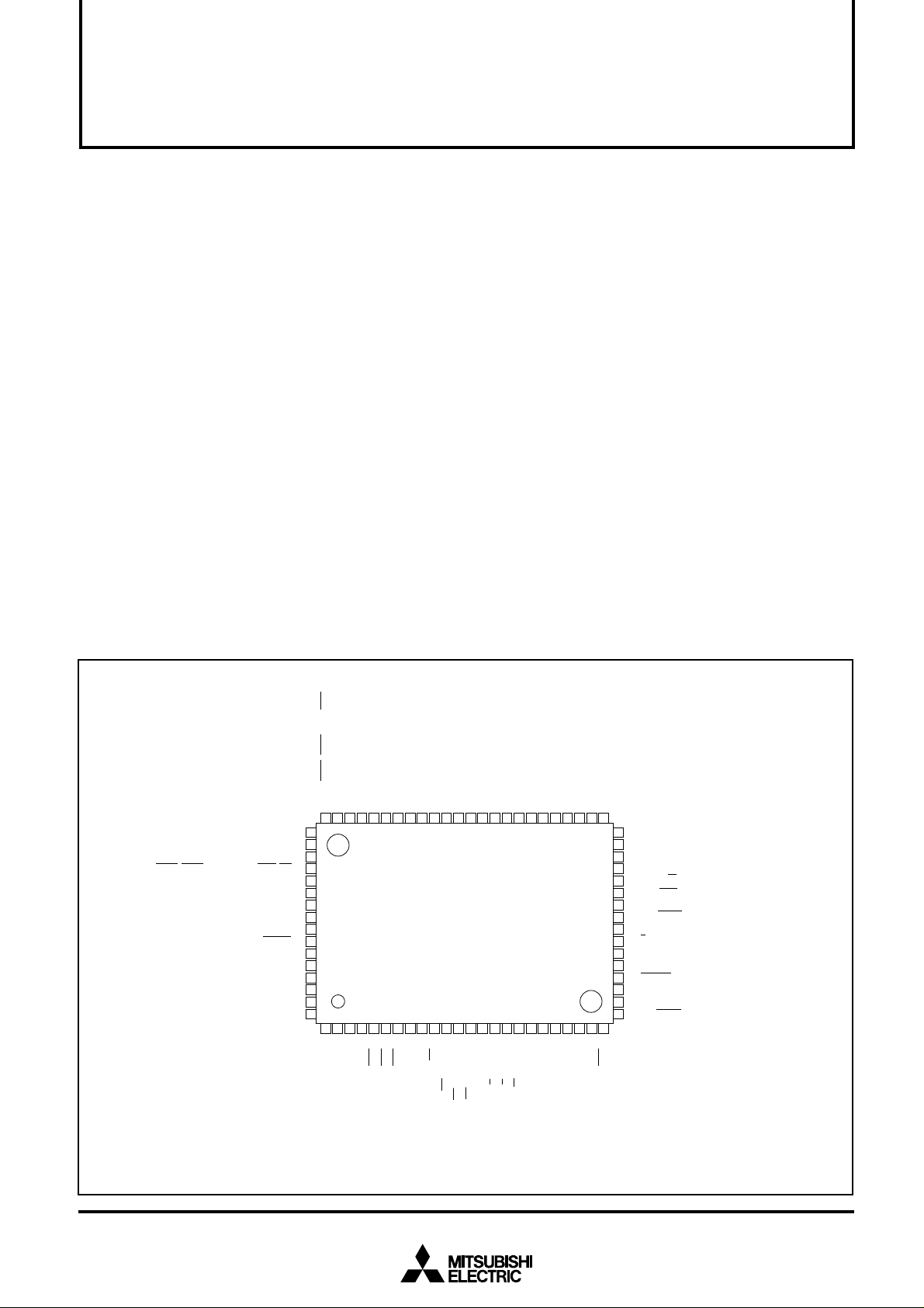
M37753M6C-XXXFP PIN CONFIGURATION (TOP VIEW)
P12/A10/D10
P11/A9/D9
P10/A8/D8
P07/A7
P06/A6
P05/A5
P04/A4
P03/A3
P83/TXD0 ↔
P8
2/RXD0/CLKS0
P8
P7
7/AN7/ADTRG
P7
P7
P7
P7
P7
P7
1/CLK0
V
AV
V
REF
AV
V
6/AN6
5/AN5
4/AN4 ↔
3/AN3 ↔
2/AN2
1/AN1
CC
CC
SS
SS
P80/CTS0/RTS0/CLKS1/DA0/INT3/KI4 ↔
P00/A0
↔ P01/A1
↔
↔ P87/TXD1
↔ P86/RXD1
↔ P85/CLK1
↔ P84/CTS1/RTS1/DA1/INT4
64636261605958575655545352
65
66
↔
67
↔
68
69
70
71
→
72
73
74
↔
75
↔
76
↔
77
78
79
↔
80
↔
123456789
↔
↔
7/TB2IN
P70/AN0
P6
M37753M6C-XXXFP
↔
↔
↔
↔
4/INT2
3/INT1
6/TB1IN
P6
P6
P65/TB0IN
P6
↔
↔
↔
↔
↔ P02/A2
101112131415161718192021222324
↔
↔
↔
↔
↔
2/INT0
1/TA4IN
P6
P6
7/TA3IN/KI3
P5
0/TA4OUT/RTP13
P6
6/TA3OUT/KI2/RTP12
P5
↔
5/TA2IN/KI1/U/RTP11 ↔
P5
↔ P13/A11/D11
↔
↔
↔
51
504948474645444342
↔
↔
1/TA0IN/V/RTP01 ↔
3/TA1IN/W/RTP03 ↔
2/TA1OUT/U/RTP02
P5
P5
P5
4/TA2OUT/KI0/V/RTP10
P5
P14/A12/D12
↔
↔ P16/A14/D14
↔
↔
↔
↔
↔
7
6
5
P4
P4
P4
0/TA0OUT/W/RTP00 ↔
P5
↔ P20/A16/D0
4 ↔P43
P4
↔
↔
↔
↔
41
↔
↔
2/φ1
1/RDY
P4
P4
40
↔ P24/A20/D4
39
↔ P25/A21/D5
38
↔ P26/A22/D6
37
P27/A23/D7
↔
36
↔
P30/R/W
35
↔ P3
34
P32/ALE
↔
33
↔ P33/HLDA
32
VSS
31
→ E
30
→ XOUT
29
XIN
←
28
← RESET
27
CNVSS
26
←
BYTE
25
↔ P40/HOLD
1/BHE
P23/A19/D3
P22/A18/D2
P21/A17/D1
P17/A15/D15
P15/A13/D13
Outline 80P6N-A
Page 2
M37753M6C-XXXFP, M37753M6C-XXXHP
PRELIMINARY
Notice: This is not a final specification.
Some parametric limits are subject to change.
M37753M6C-XXXHP PIN CONFIGURATION (TOP VIEW)
↔ P86/RXD1
↔ P87/TXD1
↔ P00/A0
↔ P01/A1
4/CTS1/RTS1/DA1/INT4 ↔
P8
P8
0/CTS0/RTS0/CLKS1/DA0/INT3/KI4 ↔
P8
3/TXD0 ↔
P8
2/RXD0/CLKS0 ↔
1/CLK0 ↔
P8
AV
AV
P85/CLK1 ↔
7/AN7/ADTRG
P7
P76/AN6
5/AN5 ↔
P7
4/AN4
P7
3/AN3
P7
2/AN2
P7
1/AN1
P7
0/AN0
P7
7/TB2IN
P6
V
REF→
V
V
CC
CC
SS
SS
↔ P02/A2
↔ P04/A4
↔ P03/A3
54
55
56
57
58
59
60
61
62
63
64
65
66
67
68
69
70
71
72
↔
73
↔
M37753M6C-XXXHP
74
↔
75
↔
76
↔
77
↔
78
↔
79
↔
80
3
2
1
4/INT2 ↔
6/TB1IN ↔P65/TB0IN ↔
P6
P6
7
6
5
4
1/TA4IN ↔
P63/INT1 ↔
P62/INT0 ↔
P6
0/TA4OUT/RTP13 ↔
P6
↔ P05/A5
53
8
7/TA3IN/KI3 ↔
P5
↔ P06/A6
52
9
6/TA3OUT/KI2/RTP12 ↔
P5
↔ P07/A7
51
10
5/TA2IN/KI1/U/RTP11 ↔
P5
↔ P10/A8/D8
50
11
4/TA2OUT/KI0/V/RTP10 ↔
P5
MITSUBISHI MICROCOMPUTERS
SINGLE-CHIP 16-BIT CMOS MICROCOMPUTER
↔ P21/A17/D1
↔ P20/A16/D0
↔ P17/A15/D15
↔ P16/A14/D14
↔ P15/A13/D13
↔ P14/A12/D12
↔ P13/A11/D11
↔ P12/A10/D10
↔ P11/A9/D9
49
12
3/TA1IN/W/RTP03 ↔
P5
48
13
2/TA1OUT/U/RTP02 ↔
P5
47
14
1/TA0IN/V/RTP01 ↔
P5
45
46
16
15
7 ↔P46 ↔P45 ↔P44 ↔
P4
0/TA0OUT/W/RTP00 ↔
P5
41
42
43
44
40
↔ P22/A18/D2
39
↔ P23/A19/D3
38
↔ P24/A20/D4
37
↔ P25/A21/D5
36
↔ P26/A22/D6
35
↔ P27/A23/D7
34
↔ P3
0/R/W
33
↔ P3
1/BHE
32
↔ P3
2/ALE
31
↔ P33/HLDA
30
VSS
29
→
E
→
XOUT
28
27
←
XIN
26
←
RESET
25
CNVSS
24
←
BYTE
23
↔
P40/HOLD
22
↔
P41/RDY
↔
P42/φ1
21
20
19
18
17
3 ↔
P4
Outline 80P6Q-A
Differences between M37753M6C-XXXFP and M37753M6C-XXXHP
Product
M37753M6C-XXXFP
M37753M6C-XXXHP
80-pin QFP (80P6N-A)
80-pin fine pitch QFP (80P6Q-A)
Package
2
Page 3
PRELIMINARY
Notice: This is not a final specification.
Some parametric limits are subject to change.
MITSUBISHI MICROCOMPUTERS
M37753M6C-XXXFP, M37753M6C-XXXHP
SINGLE-CHIP 16-BIT CMOS MICROCOMPUTER
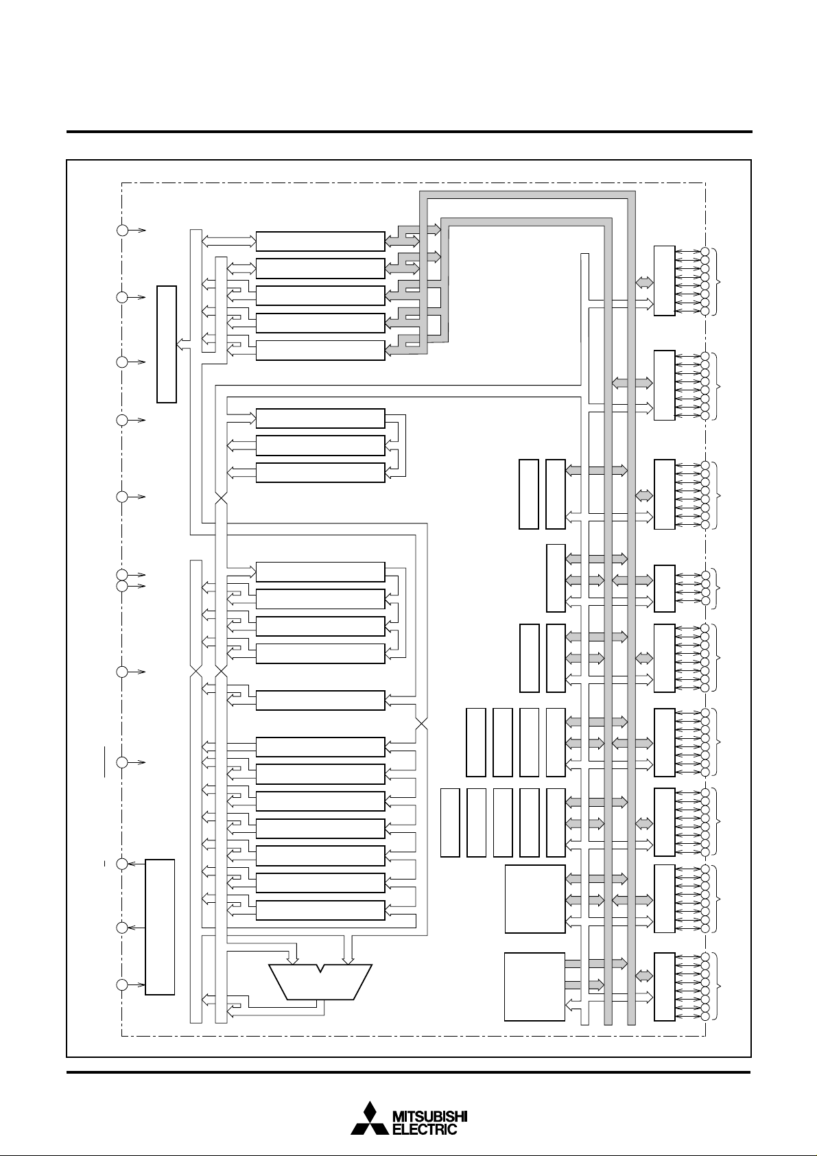
Data Bus(Even)
BYTE
Bus width
select input
VREF
Reference
voltage input
CC
(5V)
AV
SS
(0V)
AV
CNVSS
SS
V
(0V)
Instruction Register(8)
Data Buffer DB
Data Buffer DB
H(8)
L(8)
Instruction Queue Buffer Q0(8)
1
Instruction Queue Buffer Q
Instruction Queue Buffer Q
(8)
2
(8)
Incrementer(24)
Program Address Register PA(24)
Data Address Register DA(24)
Incrementer/Decrementer(24)
Program Counter PC(16)
Program Bank Register PG(8)
Data Bus(Odd)
Address Bus
Converter(8)
1
D-A
Converter(8)
0
D-A
A-D Converter(10)
(8)
P0
(8)
P1
(8)
P2
P3(4)
port P0
Input/Output
port P1
Input/Output
port P2
Input/Output
port P3
Input/Output
CC
V
(5V)
RESET
Reset input
E
Enable output
OUT
X
Clock output
Clock Generating Circuit
XIN
Clock input
BLOCK DIAGRAM
Data Bank Register DT(8)
Input Buffer Register IB(16)
Processor Status Register PS(11)
Direct Page Register DPR(16)
Stack Pointer S(16)
Index Register Y(16)
Index Register X(16)
Accumulator B(16)
Accumulator A(16)
Arithmetic Logic
Unit(16)
WatchdogTimer
Timer TA3(16)
Timer TA4(16)
UART1(9)
Timer TB1(16)
Timer TB2(16)
Timer TA1(16)
Timer TA2(16)
RAM
2048 bytes
ROM
48 Kbytes
UART0(9)
Timer TB0(16)
Timer TA0(16)
P4(8)
P8(8) P7(8) P6(8) P5(8)
port P4
Input/Output
port P5
Input/Output
port P6
Input/Output
port P7
Input/Output
port P8
Input/Output
3
Page 4
PRELIMINARY
Notice: This is not a final specification.
Some parametric limits are subject to change.
FUNCTIONS
Number of basic machine instructions
Instruction execution time
Memory size
Input/Output ports
Multiple-function timers
Serial I/O
A-D converter
D-A converter
Watchdog timer
Dead-time timer
Interrupts
Clock generating circuit
Supply voltage
Power dissipation
Input/Output characteristic
Memory expansion
Operating temperature range
Device structure
Package
M37753M6C-XXXFP, M37753M6C-XXXHP
ROM
RAM
P0–P2, P4–P8
P3
T A0, TA1, TA2, TA3, T A4
TB0, TB1, TB2
Input/Output withstand voltage
Output current
MITSUBISHI MICROCOMPUTERS
SINGLE-CHIP 16-BIT CMOS MICROCOMPUTER
FunctionsParameter
109
100 ns (the fastest instruction at external clock 40 MHz frequency)
48 Kbytes
2048 bytes
8-bit × 8
4-bit × 1
16-bit × 5
16-bit × 3
(UART or clock synchronous serial I/O) × 2
10-bit × 1 (8 channels)
8-bit × 2
12-bit × 1
8-bit × 3
5 external types, 16 internal types
(Each interrupt can be set to priority levels 0–7.)
Built-in (externally connected to a ceramic resonator or quartz crystal resonator)
5 V±10 %
125 mW(at external clock 40 MHz frequency)
5 V
5 mA
Maximum 16 Mbytes
–20 to 85 °C
CMOS high-performance silicon gate process
80-pin plastic molded QFP
4
Page 5

MITSUBISHI MICROCOMPUTERS
M37753M6C-XXXFP, M37753M6C-XXXHP
PRELIMINARY
Notice: This is not a final specification.
Some parametric limits are subject to change.
PIN DESCRIPTION
NamePin
VCC, VSS
CNVSS
RESET
XIN
XOUT
E
BYTE
(Note)
AVCC,
AVSS
VREF
P00–P07
P10–P17
P20–P27
P30–P33
P40–P47
P50–P57
P60–P67
P70–P77
P80–P87
Note: It is impossible to change the input level of the BYTE pin in each bus cycle. In other words, bus width cannot be switched dynamically. Fix the input
level of the BYTE pin to “H” or “L” according to the bus width used.
Power supply
CNVSS input
Reset input
Clock input
Clock output
Enable output
Bus width select input
Analog supply input
Reference voltage input
I/O port P0
I/O port P1
I/O port P2
I/O port P3
I/O port P4
I/O port P5
I/O port P6
I/O port P7
I/O port P8
Input/
Output
Input
Input
Input
Output
Output
Input
Input
I/O
I/O
I/O
I/O
I/O
I/O
I/O
I/O
I/O
Supply 5 V±10 % to VCC and 0 V to VSS.
This pin controls the processor mode. Connect to VSS for single-chip mode or memory
expansion mode. Connect to VCC for microprocessor mode.
This is reset input pin. The microcomputer is reset when supplying “L” level to this
pin.
These are I/O pins of internal clock generating circuit. Connect a ceramic or quartz-
crystal resonator between XIN and XOUT. When an external clock is used, the clock
source should be connected to the XIN pin and the XOUT pin should be left open.
Data or instruction read, data write are performed when output from this pin is “L”.
This pin determines whether the external data bus is 8-bit width or 16-bit width for
memory expansion mode or microprocessor mode. The width is 16 bits when “L”
signal inputs and 8 bits when “H” signal inputs.
Power supply for the A-D converter and the D-A converter. Connect AVCC to VCC
and AVSS to VSS externally.
This is reference voltage input pin for the A-D converter and the D-A converter.
In single-chip mode, port P0 is an 8-bit I/O port. This port has an I/O direction
register and each pin can be programmed for input or output. These ports are in
the input mode when reset. Address (A0–A7) is output in memory expansion mode
or microprocessor mode.
In single-chip mode, these pins have the same functions as port P0. When the
BYTE pin is set to “L” in memory expansion mode or microprocessor mode and
external data bus is 16-bit width, high-order data (D8–D15) is input or output if E
output is “L” and an address (A8–A15) is output if E output is “H”. When the BYTE
pin is set to “H” and an external data bus is 8-bit width, only address (A8–A15) is
output.
In single-chip mode, these pins have the same functions as port P0. In memory
expansion mode or microprocessor mode, low-order data (D0–D7) is input or output
when E output is “L” and an address (A16–A23) is output when E output is “H”.
In single-chip mode, these pins have the same functions as port P0. In memory
expansion mode or microprocessor mode, R/W, BHE , ALE, and HLDA signals are
output.
In single-chip mode, these pins have the same functions as port P0. In memory
expansion mode or micro processor mode, P40, P41, and P42 become HOLD and
RDY input pins, and clock
same as in single-chip mode. In memory expansion mode, P42 can be programmed as I/O port.
In addition to having the same functions as port P0 in single-chip mode, these pins
also function as I/O pins for timer A0, timer A1, timer A2, timer A3, output pins for
motor drive waveform, and input pins for key input interrupt.
In addition to having the same functions as port P0 in single-chip mode, these pins
also function as I/O pins for timer A4, input pins for external interrupt input INT0,
INT1, and INT2, and input pins for timer B0, timer B1, and timer B2, and output pin
for motor drive wave form.
In addition to having the same functions as port P0 in single-chip mode, these pins
also function as input pins for A-D converter.
In addition to having the same functions as port P0 in single-chip mode, these pins
also function as I/O pins for UART0, UART1, output pins for D-A converter, and
input pins for INT3, INT4.
SINGLE-CHIP 16-BIT CMOS MICROCOMPUTER
Functions
φ
1 output pin respectively. Functions of other pins are the
5
Page 6

PRELIMINARY
Notice: This is not a final specification.
Some parametric limits are subject to change.
MITSUBISHI MICROCOMPUTERS
M37753M6C-XXXFP, M37753M6C-XXXHP
SINGLE-CHIP 16-BIT CMOS MICROCOMPUTER
BASIC FUNCTION BLOCKS
The M37753M6C-XXXFP and M37753M6C-XXXHP has the same
functions as the M37753M8C-XXXFP and M37753M8C-XXXHP except for the following:
(1) The ROM size is different.
(2) The function of ROM area modification is not available.
Therefore, refer to the section on the M37753M8C-XXXFP.
MEMORY
The memory map is shown in Figure 1. The address space is 16
Mbytes from addresses 016 to FFFFFF16. The address space is divided into 64-Kbyte units called banks. The banks are numbered
from 016 to FF16.
Internal ROM, internal RAM, and control registers for internal peripheral devices are assigned to bank 016.
000000
Bank 0
Bank 1
•
•
•
•
•
•
•
•
•
•
•
•
•
Bank FE
Bank FF
00FFFF
010000
01FFFF
FE0000
FEFFFF
FF0000
FFFFFF
16
16
16
16
16
16
16
16
16
16
16
16
000000
00007F
000080
00087F
004000
00FFFF
The 48-Kbyte area from addresses 400016 to FFFF16 is the internal
ROM.
Addresses FFD216 to FFFF16 are the RESET and interrupt vector
addresses and contain the interrupt vectors. Refer to the section on
interrupts for details.
The 2048-byte area from addresses 8016 to 87F16 contains the internal RAM. In addition to storing data, the RAM is used as stack during a subroutine call, or interrupts.
Assigned to addresses 016 to 7F16 are peripheral devices such as
I/O ports, A-D converter, D-A converter, UART, timer, and interrupt
control registers.
A 256-byte direct page area can be allocated anywhere in bank 016
using the direct page register DPR. In direct page addressing mode,
the memory in the direct page area can be accessed with two words
thus reducing program steps.
16
16
16
Internal RAM
2048 bytes
16
16
Internal ROM
48 Kbytes
16
000000
00007F
00FFD2
00FFFE
16
Peripherai devices
control registers
see Fig. 2 for
further information
16
Interrupt vector table
16
16
INT
INT
UART1 transmit
UART1 receive
UART0 transmit
UART0 receive
Timer B2
Timer B1
Timer B0
Timer A4
Timer A3
Timer A2
Timer A1
Timer A0
INT
INT
INT
Watchdog timer
DBC
BRK instruction
Zero divide
RESET
4
3
A-D
2
1
0
Fig. 1 Memory map
6
Page 7

Y
PRELIMINAR
Notice: This is not a final specification.
Some parametric limits are subject to change.
MITSUBISHI MICROCOMPUTERS
M37753M6C-XXXFP, M37753M6C-XXXHP
SINGLE-CHIP 16-BIT CMOS MICROCOMPUTER
Address (Hexadecimal notation) Address (Hexadecimal notation)
000000
000001
000002
000003
000004
000005
000006
000007
000008
000009
00000A
00000B
00000C
00000D
00000E
00000F
000010
000011
000012
000013
000014
000015
000016
000017
000018
000019
00001A
00001B
00001C
00001D
00001E
00001F
000020
000021
000022
000023
000024
000025
000026
000027
000028
000029
00002A
00002B
00002C
00002D
00002E
00002F
000030
000031
000032
000033
000034
000035
000036
000037
000038
000039
00003A
00003B
00003C
00003D
00003E
00003F
Port P0 register
Port P1 register
Port P0 direction register
Port P1 direction register
Port P2 register
Port P3 register
Port P2 direction register
Port P3 direction register
Port P4 register
Port P5 register
Port P4 direction register
Port P5 direction register
Port P6 register
Port P7 register
Port P6 direction register
Port P7 direction register
Port P8 register
Port P8 direction register
Waveform output mode register
Dead-time timer
Pulse output data register 1
Pulse output data register 0
A-D control register 0
A-D control register 1
A-D register 0
A-D register 1
A-D register 2
A-D register 3
A-D register 4
A-D register 5
A-D register 6
A-D register 7
UART0 transmit/receive mode register
UART0 baud rate register
UART0 transmit buffer register
UART0 transmit/receive control register 0
UART0 transmit/receive control register 1
UART0 receive buffer register
UART1 transmit/receive mode register
UART1 baud rate register
UART1 transmit buffer register
UART1 transmit/receive control register 0
UART1 transmit/receive control register 1
UART1 receive buffer register
000040
000041
000042
000043
000044
000045
000046
000047
000048
000049
00004A
00004B
00004C
00004D
00004E
00004F
000050
000051
000052
000053
000054
000055
000056
000057
000058
000059
00005A
00005B
00005C
00005D
00005E
00005F
000060
000061
000062
000063
000064
000065
000066
000067
000068
000069
00006A
00006B
00006C
00006D
00006E
00006F
000070
000071
000072
000073
000074
000075
000076
000077
000078
000079
00007A
00007B
00007C
00007D
00007E
00007F
Count start register
One-shot start register
Up-down register
Timer A write register
Timer A0 register
Timer A1 register
Timer A2 register
Timer A3 register
Timer A4 register
Timer B0 register
Timer B1 register
Timer B2 register
Timer A0 mode register
Timer A1 mode register
Timer A2 mode register
Timer A3 mode register
Timer A4 mode register
Timer B0 mode register
Timer B1 mode register
Timer B2 mode register
Processor mode register 0
Processor mode register 1
Watchdog timer register
Watchdog timer frequency select register
Comparator function select register
Reserved area (Note)
Comparator result register
Reserved area (Note)
D-A register 0
D-A register 1
Particular function select register 0
Particular function select register 1
INT4 interrupt control register
INT3 interrupt control register
A-D interrupt control register
UART0 trasmit interrupt control register
UART0 receive interrupt control register
UART1 trasmit interrupt control register
UART1 receive interrupt control register
Timer A0 interrupt control register
Timer A1 interrupt control register
Timer A2 interrupt control register
Timer A3 interrupt control register
Timer A4 interrupt control register
Timer B0 interrupt control register
Timer B1 interrupt control register
Timer B2 interrupt control register
INT0 interrupt control register
INT1 interrupt control register
INT2 interrupt control register
Fig. 2 Location of peripheral devices and interrupt control registers
Note: Do not write to this address.
7
Page 8

M37753M6C-XXXFP, M37753M6C-XXXHP
PRELIMINARY
Notice: This is not a final specification.
Some parametric limits are subject to change.
ELECTRICAL CHARACTERISTICS
The M37753M6C-XXXFP and M37753M6C-XXXHP has the same
function as the M37753M8C-XXXFP and M37753M8C-XXXHP in for
the following :
(1) ABSOLUTE MAXIMUM RATINGS
(2) RECOMMENDED OPERATING CONDITIONS
(3) ELECTRICAL CHARACTERISTICS
(4) PERIPHERAL DEVICE INPUT/OUTPUT TIMING
(5) TIMING REQUIREMENTS
(6) SWITCHING CHARACTERISTICS
Therefore, refer to the corresponding section on the M37753M8CXXXFP.
ADDRESSING MODES AND INSTRUCTION SET
The M37753M6C-XXXFP and M37753M6C-XXXHP have 29 pow erful addressing modes; 1 addressing mode is added to the basis of
the 7700 series. Refer to the “7751 Series Software Manual” for the
details.
MITSUBISHI MICROCOMPUTERS
SINGLE-CHIP 16-BIT CMOS MICROCOMPUTER
INSTRUCTION SET
The M37753M6C-XXXFP and M37753M6C-XXXHP have the extended instruction set; 6 instructions are added to the instruction set
of 7700 series. The object code of this extended instruction set is
upwards compatible to that of 7700 series instruction set.
Refer to the “7751 Series Software Manual” for the details.
SHORTENING NUMBER OF INSTRUCTION EXECUTION CYCLES
Shortening number of instruction execution cycles is realized in the
M37753M6C-XXXFP and M37753M6C-XXXHP owing to modifications of the instruction execution algorithm and the CPU circuit, and
others.
Refer to the “7751 Series Software Manual” about the number of instruction execution cycles.
DATA REQUIRED FOR MASK ROM ORDERING
Please send the following data for mask orders:
<M37753M6C-XXXFP>
(1) M37753M6C-XXXFP mask ROM order confirmation form
(2) 80P6N mark specification form
(3) ROM data (EPROM 3 sets)
<M37753M6C-XXXHP>
(1) M37753M6C-XXXHP mask ROM order confirmation form
(2) 80P6Q mark specification form
(3) ROM data (EPROM 3 sets)
8
Page 9

GZZ–SH00–82B<85A0>
Mask ROM number
7700 FAMILY MASK ROM ORDER CONFIRMATION FORM
SINGLE-CHIP 16-BIT MICROCOMPUTER
M37753M6C-XXXFP
M37753M6C-XXXHP
MITSUBISHI ELECTRIC
Note : Please fill in all items marked
Company
Customer
1. Confirmation
Specify the name of the product being ordered.
Three sets of EPROMs are required for each pattern (Check @ in the appropriate box).
If at least two of the three sets of EPROMs submitted contain the identical data, we will produce masks based on this data.
We shall assume the responsibility for errors only if the mask ROM data on the products we produce differ from this data.
Thus, the customer must be especially careful in verifying the data contained in the EPROMs submitted.
name
Date
issued
Date:
TEL
( )
Date:
Section head
signature
Receipt
Responsible
officer
Issuance
signatures
Supervisor
signature
Supervisor
Checksum code for entire EPROM areas
EPROM Type :
27512
0000
0010
4000
DATA
2. STP instruction option
One of the following sets of data should be written to the option data address (1016) of the EPROM you have ordered.
Check @ in the appropriate box.
STP instruction enable
STP instruction disable
3. Mark specification
Mark specification must be submitted using the correct form for the type of package being ordered fill out the appropriate
80P6N Mark Specification Form (for M37753M6C-XXXFP), 80P6Q Mark Specification Form (for M37753M6C-XXXHP)
and attach to the Mask ROM Order Confirmation Form.
4. Comments
48K
FFFF
DATA
0116
0016
27101
00000
00010
14000
48K
1FFFF
Address 1016
Address 1016
(1) Set “FF16” in the shaded area.
Address 0
(2)
on model designation and options.This area must be
written with the data shown below.
Details for option data are given next in the section
describing the STP instruction option.
Address and data are written in hexadecimal notation.
4D
33
37
37
35
33
4D
36
(hexadecimal notation)
16 to 1016 are the area for storing the data
Address
0
1
2
3
4
5
6
7
43
2D
FF
FF
FF
FF
FF
FF
Address
8
9
A
B
C
D
E
F
Option data
Address
10
Page 10

80P6N (80-PIN QFP) MARK SPECIFICATION FORM
Mitsubishi IC catalog name
Please choose one of the marking types below (A, B, C), and enter the Mitsubishi IC catalog name and the special mark (if needed).
A. Standard Mitsubishi Mark
64
65
Mitsubishi product number
(6-digit, or 7-digit)
80
1
41
40
25
24
B. Customer’s Parts Number + Mitsubishi IC Catalog Name
64
65
80
1
41
40
25
24
Mitsubishi IC catalog name
Customer ’s Parts Number
Note : The fonts and size of characters are standard Mitsubishi type.
Mitsubishi IC catalog name
Notes 1 : The mark field should be written right aligned.
2 : The fonts and size of characters are standard Mitsubishi type.
3 : Customer’s parts number can be up to 14 alphanumeric char-
acters for capital letters, hyphens, commas, periods and so on.
4 : If the Mitsubishi logo is not required, check the box below.
Mitsubishi logo is not required
C. Special Mark Required
64
65
80
1
Notes1 :If special mark is to be printed, indicate the desired lay-
41
out of the mark in the left figure. The layout will be
duplicated technically as close as possible.
40
Mitsubishi product number (6-digit, or 7-digit) and Mask
ROM number (3-digit) are always marked for sorting the
products.
2 : If special character fonts (e,g., customer ’s trade mark
logo) must be used in Special Mark, check the box below.
25
24
For the new special character fonts, a clean font original
(ideally logo drawing) must be submitted.
Special character fonts required
Page 11

Keep safety first in your circuit designs!
• Mitsubishi Electric Corporation puts the maximum effort into making semiconductor products better and more reliable, but there is always the possibility that trouble may occur with them. Trouble with
semiconductors may lead to personal injury, fire or property damage. Remember to give due consideration to safety when making your circuit designs, with appropriate measures such as (i) placement of
substitutive, auxiliary circuits, (ii) use of non-flammable material or (iii) prevention against any malfunction or mishap.
Notes regarding these materials
• These materials are intended as a reference to assist our customers in the selection of the Mitsubishi semiconductor product best suited to the customer’s application; they do not convey any license under any
intellectual property rights, or any other rights, belonging to Mitsubishi Electric Corporation or a third party.
• Mitsubishi Electric Corporation assumes no responsibility for any damage, or infringement of any third-party’s rights, originating in the use of any product data, diagrams, charts or circuit application examples
contained in these materials.
• All information contained in these materials, including product data, diagrams and charts, represent information on products at the time of publication of these materials, and are subject to change by Mitsubishi
Electric Corporation without notice due to product improvements or other reasons. It is therefore recommended that customers contact Mitsubishi Electric Corporation or an authorized Mitsubishi Semiconductor
product distributor for the latest product information before purchasing a product listed herein.
• Mitsubishi Electric Corporation semiconductors are not designed or manufactured for use in a device or system that is used under circumstances in which human life is potentially at stake. Please contact
Mitsubishi Electric Corporation or an authorized Mitsubishi Semiconductor product distributor when considering the use of a product contained herein for any specific purposes, such as apparatus or systems for
transportation, vehicular, medical, aerospace, nuclear, or undersea repeater use.
• The prior written approval of Mitsubishi Electric Corporation is necessary to reprint or reproduce in whole or in part these materials.
• If these products or technologies are subject to the Japanese export control restrictions, they must be exported under a license from the Japanese government and cannot be imported into a country other than the
approved destination.
Any diversion or reexport contrary to the export control laws and regulations of Japan and/or the country of destination is prohibited.
• Please contact Mitsubishi Electric Corporation or an authorized Mitsubishi Semiconductor product distributor for further details on these materials or the products contained therein.
© 1999 MITSUBISHI ELECTRIC CORP.
New publication, effective Apr. 1999.
Specifications subject to change without notice.
Page 12

REVISION DESCRIPTION LIST M37753M6C-XXXFP/HP DATA SHEET
Rev. Rev.
No. date
1.0 First Edition 971114
1.01 The following are added: 980528
•MASK ROM ORDER CONFIRMATION FORM
•MARK SPECIFICATION FORM
2.00 (1) For the “timer A write flag (address 4516)”, it’s name and it’s bit name are corrected: 990428
• New register name: timer A write register
• Related page: page 7
Revision Description
(1/1)
 Loading...