

Page 1

MITSUBISHI MICROCOMPUTERS
M37753FFCFP
PRELIMINARY
Notice: This is not a final specification.
Some parametric limits are subject to change.
DESCRIPTION
The M37753FFCFP and the M37753FFCHP are single-chip microcomputers designed with high-performance CMOS silicon gate technology, including the internal flash memory. These are housed in
80-pin plastic molded QFP.
These microcomputers have a CPU and a bus interface unit. The
CPU is a 16-bit parallel processor that can also be switched to perform 8-bit parallel processing, and the bus interface unit enhances
the memory access efficiency to execute instructions fast.
In addition to the 7700 Family basic instructions, the M37753FFCFP
and the M37753FFCHP have 6 special instructions which contain instructions for signed multiplication/division; these added instructions
improve the servo arithmetic performance to control hard disk drives
and so on.
These microcomputers also include the flash memory, RAM, multiple-function timers, motor control function, serial I/O, A-D conv erter ,
D-A converter, and so on.
The internal flash memory can be programed and erased by using a
PROM programmer or by control of the central processing unit
(CPU). Therefore, these microcomputers can change the program
easily even after they are mounted on the board.
SINGLE-CHIP 16-BIT CMOS MICROCOMPUTER FLASH MEMORY VERSION
M37753FFCHP
APPLICATION
Control devices for personal computer peripheral equipment such as
CD-ROM drives, hard disk drives, high density FDD, printers
Control devices for office equipment such as copiers and facsimiles
Control devices for industrial equipment such as communication and
measuring instruments
Control devices for equipment required for motor control such as inverter air conditioner and general purpose inverter
DISTINCTIVE FEATURES
<Microcomputer mode>
Number of basic machine instructions .................................... 109
•
(103 basic instructions of 7700 Family + 6 special instructions)
Memory size Flash memory ................................ 120 Kbytes
•
Instruction execution time
•
The fastest instruction at 40 MHz frequency ...................... 100 ns
Single power supply .......................................................5V ±10 %
•
Low power dissipation (at 40 MHz frequency) .......125 mW (Typ.)
•
Interrupts ........................................................... 21 types, 7 levels
•
Multiple-function 16-bit timer ................................................... 5+3
•
(three-phase motor drive waveform or pulse motor control waveform output)
Serial I/O (UART or clock synchronous) ..................................... 2
•
10-bit A-D converter ............................................8-channel inputs
•
8-bit D-A converter ............................................ 2-channel outputs
•
12-bit watchdog timer
•
Programmable input/output (ports P0—P8) .............................. 68
•
Small package [M37753FFCHP]
•
................................... 80-pin fine pitch QFP (lead pitch : 0.5 mm)
<Flash memory mode>
Supply voltage...................................................VCC = 5 V ± 10 %
•
Program/Erase voltage...................................... VPP = 12 V ± 5 %
•
Programming method........................ Programming in unit of byte
•
Erasing method .............................................................................
•
Batch erasing and 2-division-block erasing (in CPU reprogramming mode)
Program/Erase control by software command
•
Number of times for programming/erasing.............................. 100
•
RAM................................................3968 bytes
Page 2
PRELIMINARY
Notice: This is not a final specification.
Some parametric limits are subject to change.
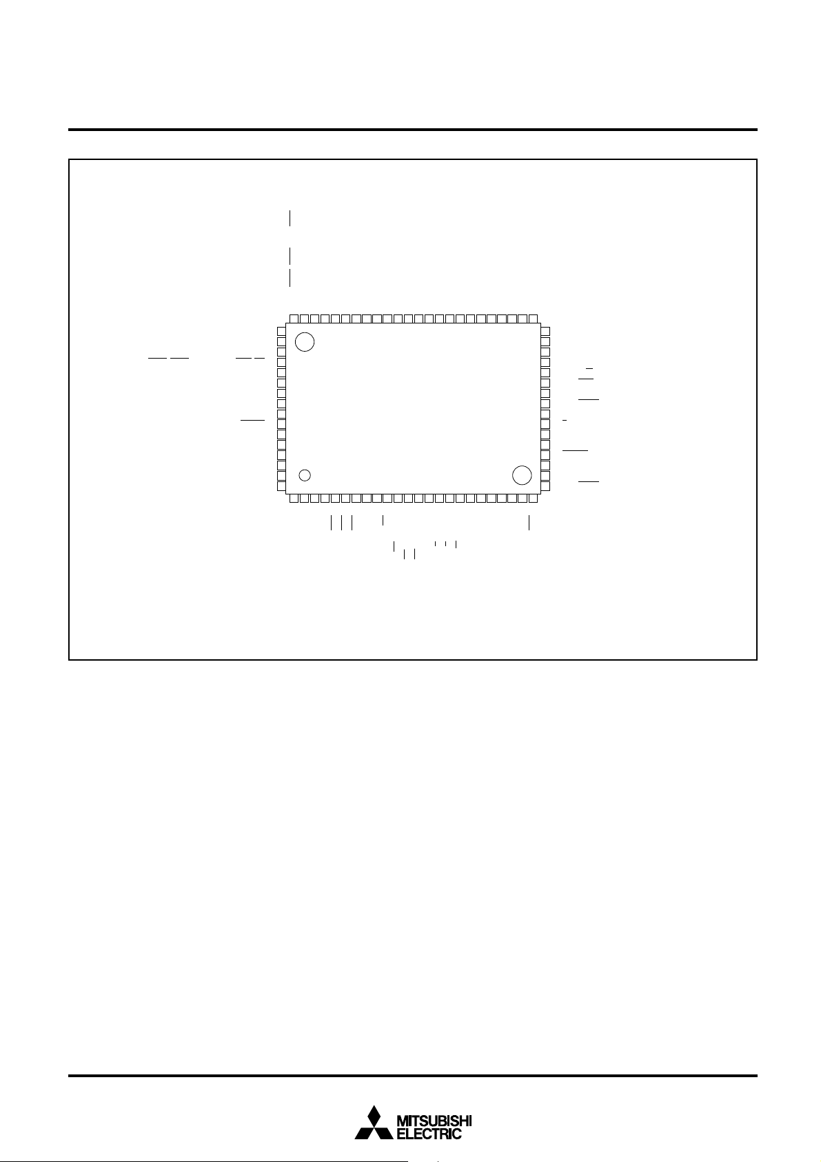
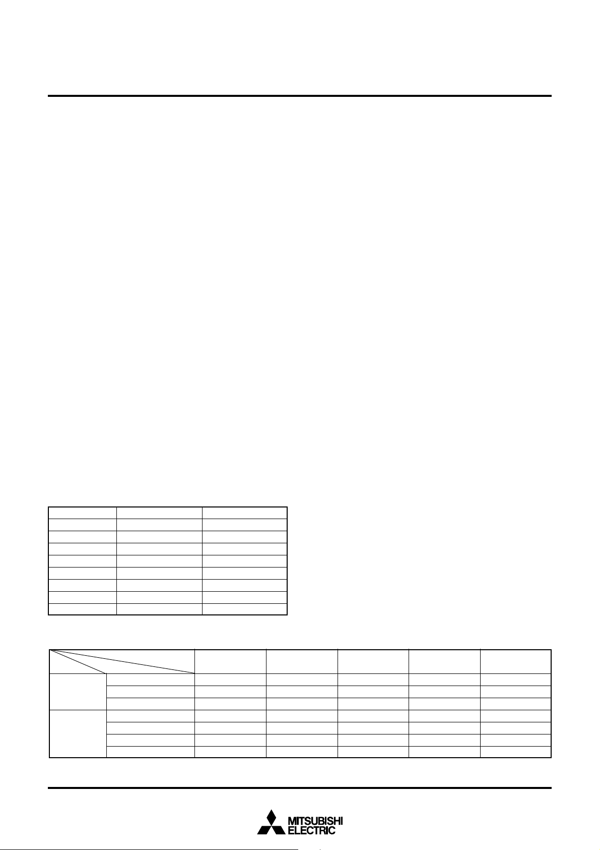
M37753FFCFP PIN CONFIGURATION (TOP VIEW)
P83/TXD0 ↔
P8
2/RXD0
/CLKS0 ↔
P8
1
P7
7
/AN7/AD
/CLK0 ↔
AV
AV
P7
6
P7
5
P7
4
P7
3
P7
2
P7
1
V
CC
CC
V
REF
SS
V
SS
TRG
/AN
6
/AN5 ↔
/AN4 ↔
/AN3 ↔
/AN2 ↔
/AN1 ↔
→
↔
↔
P80/CTS0/RTS0/CLKS1/DA0/INT3/KI4 ↔
SHINGLE-CHIP 16-BIT CMOS MICROCOMPUTER FLASH MEMORY VERSION
4
/INT
1
/DA
1
/RTS
1
1
1
1
D
D
X
0
X
/A
/T
/R
/CLK
/CTS
4
↔ P8
64636261605958575655545352
65
66
67
68
69
70
71
72
73
74
75
76
77
78
79
80
0
7
6
5
↔ P0
↔ P8
↔ P8
↔ P8
4
1
3
2
/A
/A
/A
/A
4
1
3
2
P0
↔ P0
↔ P0
↔
↔ P0
M37753FFCFP
123456789
↔
0
/AN
0
P7
↔
IN
/TB2
7
P6
↔
IN
/TB1
6
P6
↔
IN
/TB0
5
P6
↔
2
/INT
4
P6
↔
1
/INT
3
P6
↔
0
/INT
2
P6
↔
IN
/TA4
1
P6
↔
3
/RTP1
OUT
/TA4
0
P6
8
/D
7
8
6
5
/A
/A
/A
/A
7
0
6
5
P1
P0
P0
↔
↔ P0
↔
↔
101112131415161718192021222324
↔
↔
↔
↔
1
0
2
3
/KI
IN
/RTP1
2
/V/RTP1
/U/RTP1
/TA3
0
1
/KI
7
/KI
/KI
P5
OUT
IN
OUT
/TA3
/TA2
6
5
/TA2
4
P5
P5
P5
10
11
9
/D
/D
/D
10
9
11
/A
/A
/A
2
1
3
P1
↔
↔ P1
↔ P1
51
504948474645444342
↔
↔
↔
3
2
1
/V/RTP0
/U/RTP0
/W/RTP0
IN
IN
OUT
/TA0
/TA1
1
3
/TA1
2
P5
P5
P5
12
/D
/D
/D
14
13
12
/A
/A
/A
6
5
4
P1
↔ P1
↔ P1
↔
↔
↔
↔
0
7
6
P4
P4
/W/RTP0
OUT
/TA0
0
P5
15
/D
15
/A
7
P1
↔
↔
5
P4
14
13
MITSUBISHI MICROCOMPUTERS
M37753FFCFP
M37753FFCHP
1
3
2
0
/D
/D
/D
/D
17
19
18
16
/A
/A
/A
/A
1
3
2
0
P2
P2
P2
↔
↔
↔ P2
↔
41
40
↔ P24/A20/D
39
↔ P25/A21/D
38
↔ P26/A22/D
37
↔
36
↔
35
↔
34
↔
33
↔ P33/HLDA
32
V
31
→ E
30
→ X
29
←
28
← RESET
27
26
←
25
↔ P40/HOLD
↔
↔
↔
↔
1
4
3
/φ
P4
P4
2
/RDY
1
P4
P4
P27/A23/D
P30/R/W
P31/BHE
P32/ALE
SS
OUT
X
IN
CNV
SS
BYTE
4
5
6
7
Outline 80P6N-A
2
Page 3
PRELIMINARY
Notice: This is not a final specification.
Some parametric limits are subject to change.
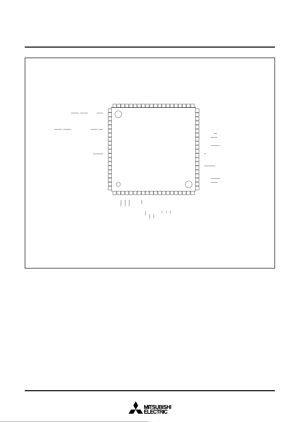
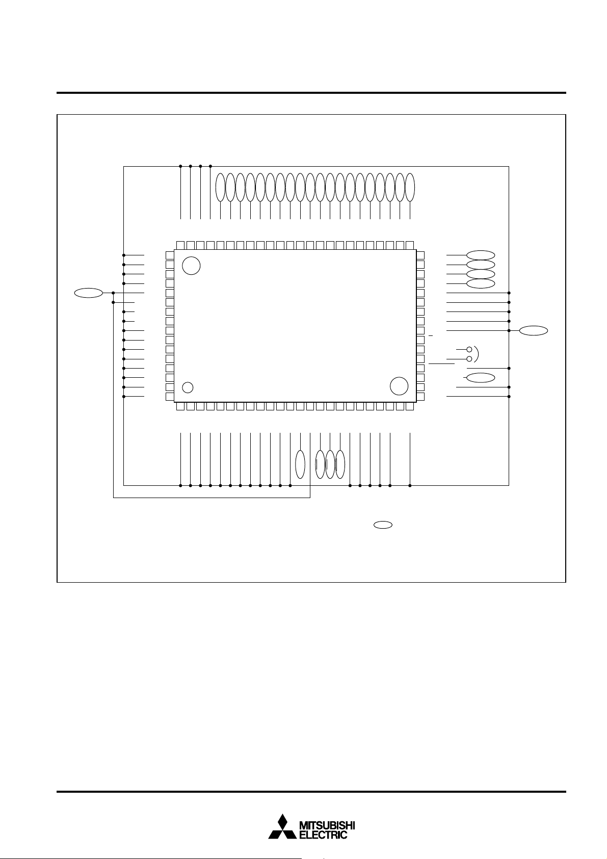
M37753FFCHP PIN CONFIGURATION (TOP VIEW)
4/CTS1/RTS1/DA1/INT4 ↔
P8
0/CTS0/RTS0/CLKS1/DA0/INT3/KI4 ↔
P8
P85/CLK1 ↔
P8
2/RXD0/CLKS0
P8
P8
7/AN7/ADTRG ↔
P7
P76/AN6 ↔
P7
P7
P7
P7
P7
P7
7/TB2IN ↔
P6
3/TXD0 ↔
1/CLK0 ↔
V
AV
V
AV
V
5/AN5 ↔
4/AN4 ↔
3/AN3 ↔
2/AN2 ↔
1/AN1 ↔
0/AN0 ↔
SHINGLE-CHIP 16-BIT CMOS MICROCOMPUTER FLASH MEMORY VERSION
6
5
4
/A
/A
/A
6
5
4
P0
P0
P0
↔ P01/A1
↔ P02/A2
56
57
↔
↔
↔
↔ P03/A3
52
53
54
55
M37753FFCHP
9
8
7
654
↔
↔
↔
↔
↔
↔
P63/INT1
P62/INT0
1/TA4IN
P6
0/TA4OUT/RTP13
P6
7/TA3IN/KI3
P5
6/TA3OUT/KI2/RTP12
P5
↔ P07/A7
51
10
↔
5/TA2IN/KI1/U/RTP11
P5
CC
CC
REF→
SS
SS
↔ P86/RXD1
↔ P87/TXD1
↔ P00/A0
58
59
60
61
62
63
64
↔
65
66
67
68
69
70
71
72
73
74
75
76
77
78
79
80
3
2
1
↔
↔
↔
4/INT2
6/TB1IN
5/TB0IN
P6
P6
P6
↔ P10/A8/D8
50
11
↔
4/TA2OUT/KI0/V/RTP10
P5
9
/D
9
/A
1
P1
↔
49
12
↔
3/TA1IN/W/RTP03
P5
↔ P12/A10/D10
48
13
↔
2/TA1OUT/U/RTP02
P5
11
/D
11
/A
3
P1
↔
47
14
↔
1/TA0IN/V/RTP01
P5
12
/D
12
/A
4
P1
↔
46
15
0/TA0OUT/W/RTP00 ↔
P5
13
/D
13
/A
5
P1
↔
45
16
↔
7
P4
MITSUBISHI MICROCOMPUTERS
M37753FFCFP
M37753FFCHP
0
15
14
/D
/D
/D
16
15
14
/A
/A
/A
0
7
6
P2
P1
P1
↔ P21/A17/D1
↔
↔
↔
41
42
43
44
40
17
↔
6
P4
18
5 ↔P44
P4
20
19
↔
3 ↔
P4
↔ P22/A18/D
39
↔ P23/A19/D
38
↔
P24/A20/D
37
↔
P25/A21/D
36
↔ P26/A22/D
35
↔ P27/A23/D
34
↔
P30/R/W
33
↔
P31/BHE
32
↔
P32/ALE
31
↔ P33/HLDA
30
V
29
→ E
→ X
28
27
←
X
26
← RESET
25
CNV
24
←
BYTE
23
↔
P40/HOLD
22
↔ P41/RDY
21
↔ P42/φ
SS
OUT
IN
2
3
4
5
6
7
SS
1
Outline 80P6Q-A
3
Page 4
PRELIMINARY
Notice: This is not a final specification.
Some parametric limits are subject to change.
MITSUBISHI MICROCOMPUTERS
M37753FFCFP
M37753FFCHP
SHINGLE-CHIP 16-BIT CMOS MICROCOMPUTER FLASH MEMORY VERSION
Data Bus(Even)
BYTE
Bus width
select input
REF
V
Reference
voltage input
CC
(5V)
AV
SS
(0V)
AV
SS
CNV
SS
V
(0V)
Instruction Register(8)
H
Data Buffer DB
Data Buffer DB
Instruction Queue Buffer Q0(8)
Instruction Queue Buffer Q
Instruction Queue Buffer Q
Incrementer(24)
Program Address Register PA(24)
Data Address Register DA(24)
Incrementer/Decrementer(24)
Program Counter PC(16)
Program Bank Register PG(8)
(8)
L
(8)
1
(8)
2
(8)
Data Bus(Odd)
Address Bus
Converter(8)
1
D-A
Converter(8)
0
D-A
A-D Converter(10)
(8)
P0
(8)
P1
(8)
P2
P3(4)
port P0
Input/Output
port P1
Input/Output
port P2
Input/Output
port P3
Input/Output
CC
V
(5V)
RESET
Reset input
E
Enable output
OUT
X
Clock output
IN
X
Clock input
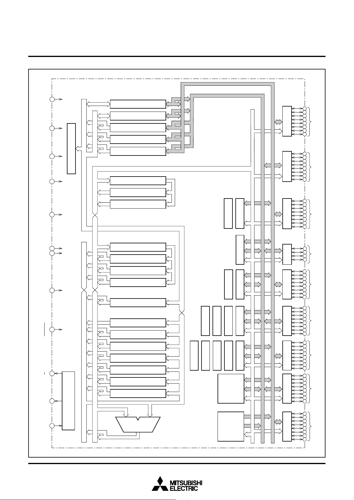
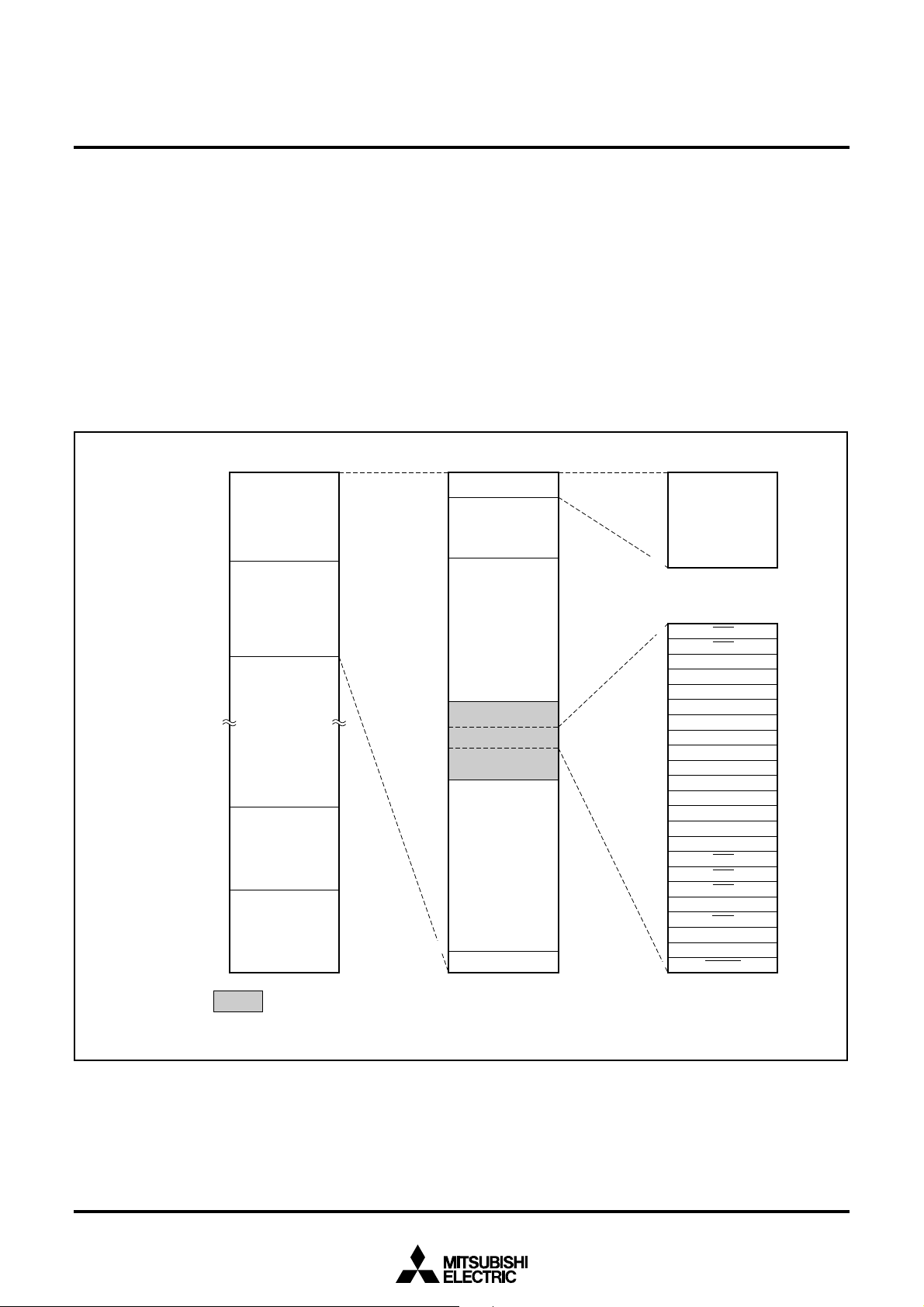
BLOCK DIAGRAM
Clock Generating Circuit
Data Bank Register DT(8)
Input Buffer Register IB(16)
Processor Status Register PS(11)
Direct Page Register DPR(16)
Stack Pointer S(16)
Index Register Y(16)
Index Register X(16)
Accumulator B(16)
Accumulator A(16)
Arithmetic Logic
Unit(16)
WatchdogTimer
Timer TA3(16)
Timer TA4(16)
UART1(9)
Timer TB1(16)
Timer TB2(16)
Timer TA1(16)
Timer TA2(16)
RAM
3968 bytes
120 Kbytes
Flash memory
UART0(9)
Timer TB0(16)
Timer TA0(16)
P4(8)
P8(8) P7(8) P6(8) P5(8)
port P4
Input/Output
port P5
Input/Output
port P6
Input/Output
port P7
Input/Output
port P8
Input/Output
4
Page 5
PRELIMINARY
Notice: This is not a final specification.
Some parametric limits are subject to change.
FUNCTIONS (Microcomputer mode)
Number of basic machine instructions
Instruction execution time
Memory size
Input/Output ports
Multiple-function timers
Serial I/O
A-D converter
D-A converter
Watchdog timer
Dead-time timer
Interrupts
Clock generating circuit
Supply voltage
Power dissipation
Input/Output characteristic
Memory expansion
Operating temperature range
Device structure
Package
Flash memory
RAM
P0–P2, P4–P8
P3
T A0, TA1, T A2, TA3, T A4
TB0, TB1, TB2
Input/Output withstand voltage
Output current
SHINGLE-CHIP 16-BIT CMOS MICROCOMPUTER FLASH MEMORY VERSION
MITSUBISHI MICROCOMPUTERS
M37753FFCFP
M37753FFCHP
FunctionsParameter
109 (103 basic instructions of 7700 Family + 6 special instructions)
100 ns (the fastest instruction at external clock 40 MHz frequency)
120 Kbytes
3968 bytes
8-bit × 8
4-bit × 1
16-bit × 5
16-bit × 3
(UART or clock synchronous serial I/O) × 2
10-bit × 1(8 channels)
8-bit × 2
12-bit × 1
8-bit × 3
5 external types, 16 internal types
(Each interrupt can be set to priority levels 0 – 7.)
Built-in (externally connected to a ceramic resonator or quartz crystal resonator)
5 V±10 %
125 mW (at external clock 40 MHz frequency)
5 V
5 mA
Maximum 16 Mbytes
–20 to 85 °C
CMOS high-performance silicon gate process
80-pin plastic molded QFP
FUNCTIONS (Flash memory mode)
Supply voltage
Program/Erase voltage
Flash memory mode
Parallel I/O mode
Programming method
Erasing method
Program/Erase control method
Command number
Number of times for Program/Erase
Serial I/O mode
CPU reprogramming mode
Parallel I/O mode
Serial I/O mode
CPU reprogramming mode
Parallel I/O mode
Serial IO mode
CPU reprogramming mode
FunctionsParameter
5 V ± 10 %
12 V ± 5 %
3 modes
(parallel I/O, serial I/O, CPU reprogramming)
Programming in unit of byte/120 Kbytes
Programming in unit of byte/120 Kbytes
Programming in unit of byte/112 Kbytes
Batch erasing/120 Kbytes
Batch erasing/120 Kbytes
Batch erasing/112 Kbytes or 2-division-block erasing
2-division-block erasing: 56-Kbyte area to be erased is selectable.
Program/Erase control by software command
7 commands
7 commands
7 commands
100
5
Page 6
MITSUBISHI MICROCOMPUTERS
M37753FFCFP
PRELIMINARY
Notice: This is not a final specification.
Some parametric limits are subject to change.
PIN DESCRIPTION (MICROCOMPUTER MODE)
NamePin
VCC, VSS
CNVSS
RESET
XIN
XOUT
E
BYTE
(Note)
AVCC,
AVSS
VREF
P00–P07
P10–P17
P20–P27
P30–P33
P40–P47
P50–P57
P60–P67
P70–P77
P80–P87
Note: It is impossible to change the input level of the BYTE pin in each bus cycle. In other words, bus width cannot be switched dynamically. Fix the input
level of the BYTE pin to “H” or “L” according to the bus width used.
Power supply
CNVSS input
Reset input
Clock input
Clock output
Enable output
Bus width select input
Analog supply input
Reference voltage input
I/O port P0
I/O port P1
I/O port P2
I/O port P3
I/O port P4
I/O port P5
I/O port P6
I/O port P7
I/O port P8
SHINGLE-CHIP 16-BIT CMOS MICROCOMPUTER FLASH MEMORY VERSION
Input/
Output
Input
Input
Input
Output
Output
Input
Input
I/O
I/O
I/O
I/O
I/O
I/O
I/O
I/O
I/O
Supply 5 V±10 % to VCC and 0 V to VSS.
This pin controls the processor mode. Connect to VSS for single-chip mode or memory
expansion mode. Connect to VCC for microprocessor mode.
This is reset input pin. The microcomputer is reset when supplying “L” level to this
pin.
These are I/O pins of internal clock generating circuit. Connect a ceramic or quartz-
crystal resonator between XIN and XOUT. When an external clock is used, the clock
source should be connected to the XIN pin and the XOUT pin should be left open.
Data or instruction read, data write are performed when output from this pin is “L”.
This pin determines whether the external data bus is 8-bit width or 16-bit width for
memory expansion mode or microprocessor mode. The width is 16 bits when “L”
signal inputs and 8 bits when “H” signal inputs.
Power supply for the A-D converter and the D-A converter. Connect AVCC to VCC
and AVSS to VSS externally.
This is reference voltage input pin for the A-D converter and the D-A converter.
In single-chip mode, port P0 is an 8-bit I/O port. This port has an I/O direction
register and each pin can be programmed for input or output. These ports are in the
input mode when reset. Address (A0–A7) is output in memory expansion mode or
microprocessor mode.
In single-chip mode, these pins have the same functions as port P0. When the
BYTE pin is set to “L” in memory expansion mode or microprocessor mode and
external data bus is 16-bit width, high-order data (D8–D15) is input or output if E
output is “L” and an address (A8–A15) is output if E output is “H”. When the BYTE
pin is set to “H” and an external data bus is 8-bit width, only address (A8–A15) is
output.
In single-chip mode, these pins have the same functions as port P0. In memory
expansion mode or microprocessor mode, low-order data (D0–D7) is input or output
when E output is “L” and an address (A16–A23) is output when E output is “H”.
In single-chip mode, these pins have the same functions as port P0. In memory
expansion mode or microprocessor mode, R/W, BHE , ALE, and HLDA signals are
output.
In single-chip mode, these pins have the same functions as port P0. In memory
expansion mode or microprocessor mode, P40, P41, and P42 become HOLD and
RDY input pins, and clock
same as in single-chip mode. In memory expansion mode , P42 can be programmed
as I/O port.
In addition to having the same functions as port P0 in single-chip mode, these pins
also function as I/O pins for timer A0, timer A1, timer A2, timer A3, output pins for
motor drive waveform, and input pins for key input interrupt.
In addition to having the same functions as port P0 in single-chip mode, these pins
also function as the I/O pin for timer A4, input pins for external interrupt input INT0,
INT1, and INT2, and input pins for timer B0, timer B1, and timer B2, and output pin
for motor drive wave form.
In addition to having the same functions as port P0 in single-chip mode, these pins
also function as input pins for A-D converter.
In addition to having the same functions as port P0 in single-chip mode, these pins
also function as I/O pins for UART0, UART1, output pins for D-A converter, and
input pins for INT3, INT4.
φ
1 output pin respectively. Functions of other pins are the
Functions
M37753FFCHP
6
Page 7
PRELIMINARY
Notice: This is not a final specification.
Some parametric limits are subject to change.
PIN DESCRIPTION (FLASH MEMORY PARALLEL I/O MODE)
Pin Name
VCC, VSS
CNVSS
BYTE
_____
RESET
XIN
XOUT
_
E
AVCC, AVSS
VREF
P00–P07
P10–P17
P20–P27
P30–P33
P40–P47
P50–P57
P60–P67
P70–P77
P80–P87
Power supply
VPP input
Bus width select input
Reset input
Clock input
Clock output
Enable output
Analog supply input
Reference voltage input
Address input (A0–A7)
Address input (A8–A15)
Data I/O (D0–D7)
Input port P3
Input port P4
Control signal input
Input port P6
Input port P7
Input port P8
SHINGLE-CHIP 16-BIT CMOS MICROCOMPUTER FLASH MEMORY VERSION
Input
/Output
Supply 5 V ± 10 % to VCC and 0 V to VSS.
—
Input
Input
Input
Input
Output
Output
Input
Input
Input
Input
Input
Input
Input
Input
Input
Connect to 5 V ± 10 % in read-only mode, connect to 12 V ± 5 % in read/write mode.
Connect to VSS.
Connect to VSS.
Connect a ceramic resonator between XIN and XOUT.
Keep it open.
Connect AVCC to VCC and AVSS to VSS.
—
Connect to VSS.
Port P0 functions as 8-bit address input (A0–A7).
Port P1 functions as 8-bit address input (A8–A15).
Function as 8-bit data’s I/O pins (D0–D7).
I/O
Connect to VSS.
Keep P42 open. Connect P40, P41, P43–P47 to VSS.
P50, P51 and P52 function as the WE, OE and CE input pins respectively. P54 functions as the
A16 input pin.
Connect to VSS.
Connect to VSS.
Connect to VSS.
Connect P53 to VCC. Connect P55, P56 and P57 to VSS.
___ __ __
MITSUBISHI MICROCOMPUTERS
M37753FFCFP
M37753FFCHP
Functions
7
Page 8
PRELIMINARY
Notice: This is not a final specification.
Some parametric limits are subject to change.
PIN DESCRIPTION (FLASH MEMORY SERIAL I/O MODE)
Pin
VCC, VSS
CNVSS
BYTE
_____
RESET
XIN
XOUT
_
E
AVCC, AVSS
VREF
P00–P07
P10–P17
P20–P27
P30–P33
P40–P43,
P47
P44
P45
P46
P50,
P52–P57
P51
P60–P67
P70–P77
P80–P87
Power supply
VPP input
Bus width select input
Reset input
Clock input
Clock output
Enable output
Analog supply input
Reference voltage input
Input port P0
Input port P1
Input port P2
Input port P3
Input port P4
BUSY output
SDA I/O
SCLK input
Input port P5
Control signal input
Input port P6
Input port P7
Input port P8
Name
SHINGLE-CHIP 16-BIT CMOS MICROCOMPUTER FLASH MEMORY VERSION
Input
/Output
—
Supply 5 V ± 10 % to VCC and 0 V to VSS.
Input
Input
Input
Input
Output
Output
Input
Input
Input
Input
Input
Input
Output
Input
Input
Input
Input
Input
Input
Connect to 12 V ± 5 %.
Connect to VSS or VCC.
Connect to VSS.
Connect a ceramic resonator between XIN and XOUT.
“H” is output.
—
Connect AVCC to VCC and AVSS to VSS.
Input an arbitrary level between the range of VSS and VCC.
Input “H” or “L”, or keep them open.
Input “H” or “L”, or keep them open.
Input “H” or “L”, or keep them open.
Input “H” or “L”, or keep them open.
Input “H” or “L” to P40, P41, P43, P47, or keep them open. Keep P42 open.
This pin is for BUSY signal output.
I/O
This pin is for serial data I/O.
This pin is for serial clock input.
Input “H” or “L”, or keep them open.
__
OE input pin
Input “H” or “L”, or keep them open.
Input “H” or “L”, or keep them open.
Input “H” or “L”, or keep them open.
MITSUBISHI MICROCOMPUTERS
M37753FFCFP
M37753FFCHP
Functions
8
Page 9
PRELIMINARY
Notice: This is not a final specification.
Some parametric limits are subject to change.
MITSUBISHI MICROCOMPUTERS
M37753FFCFP
M37753FFCHP
SHINGLE-CHIP 16-BIT CMOS MICROCOMPUTER FLASH MEMORY VERSION
BASIC FUNCTION BLOCKS
The M37753FFCFP and the M37753FFCHP have the same functions as the M37753M8C-XXXGP and the M37753M8C-XXXHP except for the following.
Therefore, refer to the section on the M37753M8C-XXXGP and the
M37753M8C-XXXHP.
(1) Flash memory is included instead of ROM.
(2) The memory size is different.
(3) The memory area modification function is different.
(4) Part of the peripheral devices control registers is different.
(Flash memory control register, flash command register , and bits
3, 4 of particular function select register 0 are added.)
000000
Bank 0
16
Bank 1
16
• • • • • • • • • • • • •
Bank FE
16
Bank FF
16
00FFFF
010000
01FFFF
FE0000
FEFFFF
FF0000
FFFFFF
16
16
16
16
16
16
16
16
000000
00007F
000080
000FFF
001000
00EFFF
00FFD2
00FFFF
010000
010FFF
01EFFF
01FFFF
MEMORY
The memory map is shown in Figure 1.
16
16
16
Internal RAM
3968 bytes
16
16
Internal
flash memory
120 Kbytes
16
16
16
16
16
16
Reserved area
16
000000
00007F
00FFD2
00FFFE
16
Peripheral devices
control registers
(Refer to Fig.2.)
16
Interrupt vector table
16
16
INT
INT
A-D conversion
UART1 transmission
UART1 receive
UART0 transmission
UART0 receive
Timer B2
Timer B1
Timer B0
Timer A4
Timer A3
Timer A2
Timer A1
Timer A0
INT
INT
INT
Watchdog timer
DBC
BRKinstruction
0 divide
RESET
4
3
2
1
0
Fig. 1 Memory map
: The flash memory area (8 Kbytes) where it is impossible to erase/modify in the CPU reprogramming mode.
(It is possible to erase/modify in the parallel I/O mode or the serial I/O mode.)
Note: The internal memory area can be changed. (Refer to the section on the memory area modification function.)
9
Page 10
Y
PRELIMINAR
Notice: This is not a final specification.
Some parametric limits are subject to change.
MITSUBISHI MICROCOMPUTERS
M37753FFCFP
M37753FFCHP
SHINGLE-CHIP 16-BIT CMOS MICROCOMPUTER FLASH MEMORY VERSION
Address (Hexadecimal notation) Address (Hexadecimal notation)
000000
000001
000002
000003
000004
000005
000006
000007
000008
000009
00000A
00000B
00000C
00000D
00000E
00000F
000010
000011
000012
000013
000014
000015
000016
000017
000018
000019
00001A
00001B
00001C
00001D
00001E
00001F
000020
000021
000022
000023
000024
000025
000026
000027
000028
000029
00002A
00002B
00002C
00002D
00002E
00002F
000030
000031
000032
000033
000034
000035
000036
000037
000038
000039
00003A
00003B
00003C
00003D
00003E
00003F
Port P0 register
Port P1 register
Port P0 direction register
Port P1 direction register
Port P2 register
Port P3 register
Port P2 direction register
Port P3 direction register
Port P4 register
Port P5 register
Port P4 direction register
Port P5 direction register
Port P6 register
Port P7 register
Port P6 direction register
Port P7 direction register
Port P8 register
Port P8 direction register
Waveform output mode register
Dead-time timer
Pulse output data register 1
Pulse output data register 0
A-D control register 0
A-D control register 1
A-D register 0
A-D register 1
A-D register 2
A-D register 3
A-D register 4
A-D register 5
A-D register 6
A-D register 7
UART0 transmit/receive mode register
UART0 baud rate register
UART0 transmit buffer register
UART0 transmit/receive control register 0
UART0 transmit/receive control register 1
UART0 receive buffer register
UART1 transmit/receive mode register
UART1 baud rate register
UART1 transmit buffer register
UART1 transmit/receive control register 0
UART1 transmit/receive control register 1
UART1 receive buffer register
000040
000041
000042
000043
000044
000045
000046
000047
000048
000049
00004A
00004B
00004C
00004D
00004E
00004F
000050
000051
000052
000053
000054
000055
000056
000057
000058
000059
00005A
00005B
00005C
00005D
00005E
00005F
000060
000061
000062
000063
000064
000065
000066
000067
000068
000069
00006A
00006B
00006C
00006D
00006E
00006F
000070
000071
000072
000073
000074
000075
000076
000077
000078
000079
00007A
00007B
00007C
00007D
00007E
00007F
Count start register
One-shot start register
Up-down register
Timer A write register
Timer A0 register
Timer A1 register
Timer A2 register
Timer A3 register
Timer A4 register
Timer B0 register
Timer B1 register
Timer B2 register
Timer A0 mode register
Timer A1 mode register
Timer A2 mode register
Timer A3 mode register
Timer A4 mode register
Timer B0 mode register
Timer B1 mode register
Timer B2 mode register
Processor mode register 0
Processor mode register 1
Watchdog timer register
Watchdog timer frequency select regsiter
Comparator function select register
Flash command register
Comparator result register
Flash memory control register
D-A register 0
D-A register 1
Particular function select register 0
Particular function select register 1
INT4 interrupt control register
INT3 interrupt control register
A-D interrupt control register
UART0 trasmit interrupt control register
UART0 receive interrupt control register
UART1 trasmit interrupt control register
UART1 receive interrupt control register
Timer A0 interrupt control register
Timer A1 interrupt control register
Timer A2 interrupt control register
Timer A3 interrupt control register
Timer A4 interrupt control register
Timer B0 interrupt control register
Timer B1 interrupt control register
Timer B2 interrupt control register
INT0 interrupt control register
INT1 interrupt control register
INT2 interrupt control register
Fig. 2 Location of peripheral devices and interrupt control registers
10
Page 11
Y
PRELIMINAR
Notice: This is not a final specification.
Some parametric limits are subject to change.
MITSUBISHI MICROCOMPUTERS
M37753FFCFP
M37753FFCHP
SHINGLE-CHIP 16-BIT CMOS MICROCOMPUTER FLASH MEMORY VERSION
Address
(
Port P0 direction register
Port P1 direction register
Port P2 direction register
Port P3 direction register
Port P4 direction register
Port P5 direction register
Port P6 direction register
Port P7 direction register
Port P8 direction register
A-D control register 0
A-D control register 1
UART 0 transmit/receive mode register
UART 1 transmit/receive mode register
UART 0 transmit/receive control register 0
UART 1 transmit/receive control register 0
UART 0 transmit/receive control register 1
UART 1 transmit/receive control register 1
Count start register
One-shot start register
Up-down register
Timer A1 mode register
Timer A2 mode register
Timer A3 mode register
Timer A4 mode register
Timer B0 mode register
Timer B1 mode register
Timer B2 mode register
Processor mode register 0
Processor mode register 1
04
(
05
(
08
(
09
(
0C
(
0D
(
10
(
11
(
14
(
1A
(
1C
(
1D
(
1E
(
1F
(
30
(
38
(
34
(
3C
(
35
(
3D
(
40
(
42
(
44
(
45
(
56
(
57
(
58
(
59
(
5A
(
5B
(
5C
(
5D
(
5E
(
5F
)
···
16
)
···
16
)
···
16
)
···
16
)
16
···
)
···
16
)
···
16
)
···
16
)
···
16
)
···Waveform output mode register 00
16
)
···Pulse output data register 1 00
16
)
···Pulse output data register 0
16
)
···
16
)
···
16
)
···
16
)
16
···
)
···
16
)
···
16
)
···
16
)
···
16
)
···
16
)
···
16
)
···
16
)
···Timer A write register
16
)
···Timer A0 mode register 00
16
)
···
16
)
···
16
)
···
16
)
16
···
)
···
16
)
···
16
)
···
16
)
16
···
)
···
16
00
00
000
0 0000
00
00
00
00
00
00
00
00
00
00
00
00
00
16
16
0000
16
16
16
16
16
16
16
0000 000
00000 ???
00000 011
16
16
100 000
100 000
00000 010
00000 010
16
00 000
00000 000
000
16
16
16
16
16
0010 000
0010 000
0010 000
00000 000
16
Address
Watchdog timer
Watchdog timer frequency select register
Comparator function select register
Comparator result register
Flash memory control register
D-A register 0
Particular function select register 0
Particular function select register 1
INT
4
interrupt control register
3
interrupt control register
INT
A-D interrupt control register
UART 0 transmit interrupt control register
UART 0 receive interrupt control register
UART 1 transmit interrupt control register
UART 1 receive interrupt control register
Timer A0 interrupt control register
Timer A1 interrupt control register
Timer A2 interrupt control register
Timer A3 interrupt control register
Timer A4 interrupt control register
Timer B0 interrupt control register
Timer B1 interrupt control register
Timer B2 interrupt control register
0
interrupt control register
INT
INT
1
interrupt control register
INT2 interrupt control register
Processor status register PS
Program bank register PG
Program counter PC
Program counter PC
H
L
Direct page register DPR
Data bank register DT
Contents of other registers and RAM are not initiallzed and must be in-
itiallzed by software.
(
)
60
···
16
(
)
61
···
16
(
)
16
64
···
(
)
66
···
16
(
)
67
···
16
)
(
···
16
68
(
)
16
6A
···D-A register 1
)
(
···
16
6C
(
)
6D
···
16
(
)
6E
···
16
)
(
···
16
6F
(
)
70
···
16
)
(
···
16
71
)
(
···
16
72
(
)
73
···
16
(
)
74
···
16
(
)
75
···
16
)
(
···
16
76
(
)
77
···
16
)
(
···
16
78
(
)
79
···
16
)
(
···
16
7A
(
)
7B
···
16
(
)
7C
···
16
(
)
7D
···
16
(
)
7E
16
···
(
)
7F
···
16
000
FFF
16
00
00
16
00
16
0000000
00
16
00
16
00
16
00
16
000 000
00000000
?000
0000
0000
0000
0000
0000
0000
0000
0000
0000
0000
0000
0000
000 000
000 000
000
000
1??
000??
16
00
Contents of FFFF
Contents of FFFE
0000
16
16
16
00
16
Fig. 3 Microcomputer internal registers status after reset
11
Page 12
PRELIMINARY
Notice: This is not a final specification.
Some parametric limits are subject to change.
MEMORY AREA MODIFICATION FUNCTION
For the M37753FFCFP and the M37753FFCHP, the internal
memory’s size and address area can be changed by setting bits 2, 3,
4 (memory allocation select bits) of the particular function select register 0 (see figure 5). Figure 4 shows the memory map when changing the internal memory area.
SHINGLE-CHIP 16-BIT CMOS MICROCOMPUTER FLASH MEMORY VERSION
MITSUBISHI MICROCOMPUTERS
M37753FFCFP
M37753FFCHP
ML0 : Memory allocation select bit 0
1
: Memory allocation select bit 1
ML
2
: Memory allocation select bit 2
ML
(ML
2, ML1, ML0) = (0, 0, 0)
Flash memory size : 120 Kbytes
RAM size : 3968 bytes
00 000016
00 008016
00 0FFF16
00 100016
01 EFFF16
01 FFFF16
FF FFFF16
(ML
Flash memory size : 48 Kbytes
RAM size : 2048 bytes
00 000016
00 008016
00 087F16
00 400016
00 FFFF16
SFR
Internal RAM 3968 bytes
Internal flash memory
120 Kbytes
(Reserved area)
External memory area
2, ML1, ML0) = (1, 0, 0)
SFR
Internal RAM 2048 bytes
External memory area
Internal flash memory
48 Kbytes
Note: The internal flash memory area becomes the external memory area in the microprocessor mode.
2, ML1, ML0) = (0, 0, 1)
(ML
Flash memory size : 92 Kbytes
RAM size : 3968 bytes
00 000016
00 008016
00 0FFF16
00 800016
01 EFFF16
01 FFFF16
FF FFFF16
00 000016
00 008016
00 087F16
00 800016
00 FFFF16
Internal RAM 3968 bytes
External memory area
Internal flash memory
92 Kbytes
(Reserved area)
External memory area
(ML
2, ML1, ML0) = (1, 0, 1)
Flash memory size : 32 Kbytes
RAM size : 2048 bytes
Internal RAM 2048 bytes
External memory area
Internal flash memory
32 Kbytes
SFR
SFR
(ML
2, ML1, ML0) = (0, 1, 0)
Flash memory size : 60 Kbytes
RAM size : 3072 bytes
00 000016
00 008016
00 0C7F16
00 100016
00 FFFF16
FF FFFF16
00 000016
00 008016
00 087F16
00 100016
00 FFFF16
Internal RAM 3072 bytes
Internal flash memory
60 Kbytes
(ML
2, ML1, ML0) = (1, 1, 0)
Flash memory size : 60 Kbytes
RAM size : 2048 bytes
Internal RAM 2048 bytes
Internal flash memory
60 Kbytes
2, ML1, ML0) = (0, 1, 1)
(ML
Flash memory size : 56 Kbytes
RAM size : 3072 bytes
SFR SFR
SFR SFR
00 000016
00 008016
00 0C7F16
00 200016
00 FFFF16
FF FFFF16
00 000016
00 008016
00 087F16
00 200016
00 FFFF16
Internal RAM 3072 bytes
Internal flash memory
56 Kbytes
External memory areaExternal memory area
(ML2, ML1, ML0) = (1, 1, 1)
Flash memory size : 56 Kbytes
RAM size : 2048 bytes
Internal RAM 2048 bytes
Internal flash memory
56 Kbytes
FF FFFF16
FF FFFF16
FF FFFF16
Fig. 4 Memory allocation (Internal memory area modification by memory allocation select bits)
12
External memory areaExternal memory areaExternal memory area External memory areaExternal memory area
FF FFFF16
Page 13
PRELIMINARY
Notice: This is not a final specification.
Some parametric limits are subject to change.
MITSUBISHI MICROCOMPUTERS
M37753FFCFP
M37753FFCHP
SHINGLE-CHIP 16-BIT CMOS MICROCOMPUTER FLASH MEMORY VERSION
76543210
0
Particular function select register 0
6C
16
Fix to “0”
External clock input select bit (Notes 1, 2)
0 : Actuated oscillation circuit; connecting resonator
1 : Stopped oscillation circuit; inputting externally generated clock
Memory allocation select bits 2, 1, 0 (Note 2)
0 0 0 : ROM 120 Kbytes, RAM 3968 bytes
Address
(
ROM : 001000
16
to 1EFFFF16, RAM : 00008016 to 000FFF
0 0 1 : ROM 92 Kbytes, RAM 3968 bytes
(
ROM:008000
16
to 01EFFF16, RAM:00008016 to 000FFF
16
0 1 0 : ROM 60 Kbytes, RAM 3072 bytes
(
ROM : 001000
16
to 00FFFF16, RAM : 00008016 to 000C7F
0 1 1 : ROM 56 Kbytes, RAM 3072 bytes
(
ROM:002000
16
to 00FFFF16, RAM:00008016 to 000C7F
16
1 0 0 : ROM 48 Kbytes, RAM 2048 bytes
(
ROM : 004000
16
to 00FFFF16, RAM : 00008016 to 00087F
1 0 1 : ROM 32 Kbytes, RAM 2048 bytes
(
ROM:008000
16
to 00FFFF16, RAM:00008016 to 00087F
16
1 1 0 : ROM 60 Kbytes, RAM 2048 bytes
(
ROM : 001000
16
to 00FFFF16, RAM : 00008016 to 00087F
1 1 1 : ROM 56 Kbytes, RAM 2048 bytes
(
ROM:002000
16
to 00FFFF16, RAM:00008016 to 00087F
16
Standby state select bit 0 (Note 1)
; when WIT or STP instruction is executed in memory expansion
or microprocessor mode
0 : Pins P0 to P3 are for external data bus.
1 : Pins P0 to P3 are for port output or port input.
)
16
)
)
16
)
)
16
)
)
16
)
Standby state select bit 1 (Notes 1, 3)
; in execution of WIT or STP instruction
0 : “H” or “L” output for pin E
1 : “H” output for pin E
STP return select bit
0 : Watchdog timer is used when returning from Stop mode
1 : Watchdog timer is not used when returning from Stop mode; the microcomputer returns at once.
Notes 1 : After the expansion function select bit (bit 5 of particular function select register 1) is “1”, bits 1, 5 and 6 can be rewritten.
2 : To set bits 1 to 4, continuous-twice-write operation must be performed to address 6C
3 : When the signal output disable select bit is “1” and bit 5 is “1”, the E pin always outputs “L” independent of bit 6’s contents
in execution of WIT or STP instruction.
Fig. 5 Particular function select register 0 bit configuration
16
.
13
Page 14
PRELIMINARY
Notice: This is not a final specification.
Some parametric limits are subject to change.
MITSUBISHI MICROCOMPUTERS
M37753FFCFP
M37753FFCHP
SHINGLE-CHIP 16-BIT CMOS MICROCOMPUTER FLASH MEMORY VERSION
FLASH MEMORY MODE
The M37753FFCFP and the M37753FFCHP have the flash memory
mode in addition to the normal operation mode (microcomputer
mode). The user can use this mode to perform read, program, and
erase operations for the internal flash memory.
The M37753FFCFP and the M37753FFCHP have three modes the
user can choose: the parallel input/output and serial input/output
mode, where the flash memory is handled by using the external programmer, and the CPU reprogramming mode, where the flash
memory is handled by the central processing unit (CPU). The following explains these modes.
Flash memory mode 1 (parallel I/O mode)
The parallel I/O mode can be selected by connecting wires as shown
in Figures 6, 7 and supplying power to the VCC and VPP pins. In this
mode, the M37753FFCFP and the M37753FFCHP operate as an
equivalent of MITSUBISHI’s CMOS flash memory M5M28F101.
However, because the M37753FFCFP and the M37753FFCHP’s internal memory has a capacity of 120 Kbytes, programming is available for addresses 0100016 to 1EFFF16, and make sure that the data
in addresses 0000016 to 00FFF16 and addresses 1F00016 to
1FFFF16 are FF16. Note also that the M37753FFCFP and the
M37753FFCHP do not contain a facility to read out a device identification code by applying a high voltage to address input (A9). Be
careful not to erratically set program conditions when using a general-purpose PROM programmer.
Table 1 shows the pin assignments when operating in the parallel
input/output mode.
Table 1. Pin assignments of M37753FFCFP and M37753FFCHP
when operating in the parallel input/output mode
VCC
VPP
VSS
Address input
Data I/O
__
CE
___
OE
___
WE
M37753FFCFP/CHP
VCC
CNVSS
VSS
Ports P0, P1, P54
Port P2
P52
P51
P50
M5M28F101
VCC
VPP
VSS
A0–A16
D0–D7
__
CE
__
OE
___
WE
Functional outline (Parallel input/output mode)
In the parallel input/output mode, the M37753FFCFP and the
M37753FFCHP allow the user to choose an operation mode between the read-only mode and the read/write mode (software command control mode) depending on the voltage applied to the VPP pin.
When VPP = VPPL, the read-only mode is selected, and the user can
choose one of three states (e.g., read, output disable, or standby) de-
___ ___
___
pending on inputs to the CE, OE, and WE pins. When VPP = VPPH,
the read/write mode is selected, and the user can choose one of four
states (e.g., read, output disable, standby, or write) depending on in-
__ __ ___
puts to the CE, OE, and WE pins. Table 2 shows assignment states
of control input and each state.
Read
The microcomputer enters the read state by driving the CE, and OE
___
__ __
pins low and the WE pin high; and the contents of memory corresponding to the address to be input to address input pins (A0–A16).
are output to the data input/output pins (D0–D7).
Output disable
The microcomputer enters the output disable state by driving the CE
___ __
__
pin low and the WE and OE pins high; and the data input/output pins
enter the floating state.
Standby
__
The microcomputer enters the standby state by driving the CE pin
high. The M37753FFCFP and the M37753FFCHP are placed in a
power-down state consuming only a minimal supply current. At this
time, the data input/output pins enter the floating state.
Write
The microcomputer enters the write state by driving the VPP pin high
(VPP = VPPH) and then the WE pin low when the CE pin is low and
__
the OE pin is high. In this state, software commands can be input
from the data input/output pins, and the user can choose program or
erase operation depending on the contents of this software command.
___ __
Table 2. Assignment sates of control input and each state
__
CE
VIL
VIL
VIH
VIL
VIL
VIH
VIL
Mode
State
Read
Read-only
Output disable
Standby
Read
Read/Write
Output disable
Standby
Write
Note: × can be VIL or VIH.
Pin
14
__
OE
VIL
VIH
×
VIL
VIH
×
VIH
___
WE
VIH
VIH
VIH
VIH
VIL
VPP
VPPL
VPPL
×
VPPL
VPPH
VPPH
×
VPPH
VPPH
Data I/O
Output
Floating
Floating
Output
Floating
Floating
Input
Page 15
PRELIMINARY
Notice: This is not a final specification.
Some parametric limits are subject to change.
MITSUBISHI MICROCOMPUTERS
M37753FFCFP
M37753FFCHP
SHINGLE-CHIP 16-BIT CMOS MICROCOMPUTER FLASH MEMORY VERSION
D0D1D2D
21
22
23
4
3
2
P4
P4
P4
3
3
41
24
1
P4
40
39
38
37
36
35
34
33
32
31
30
29
28
27
26
25
P2
4
P2
5
P2
6
P2
7
P3
0
P3
1
P3
2
P3
3
V
SS
E
X
OUT
X
IN
RESET
CNV
SS
BYTE
0
P4
D
4
D
5
D
6
D
7
V
SS
✽
V
PP
11
6
P5
12
5
P5
13
4
P5
16
A
9
14
3
P5
A0A1A2A3A4A5A6A7A8A
4
P8
P85P86P87P00P01P02P03P04P05P06P07P10P11P12P13P14P15P16P17P20P21P22P2
64
63
65
P8
3
66
P8
2
67
P8
1
68
P8
0
69
V
V
CC
AV
V
AV
REF
V
P7
P7
P7
P7
P7
P7
P7
CC
CC
SS
SS
70
71
72
73
74
7
75
6
76
5
77
4
78
3
79
2
80
1
626160595857565554535251504948474645444342
M37753FFCFP
1
2
3
4
5
6
7
8
9
0
P7
7
P6
6
P6
5
P6
4
P6
3
P6
2
P6
1
P6
0
P6
10
7
P5
A10A11A12A
15
16
17
2
1
0
P5
P5
P5
CE
OE
WE
13
18
7
P4
14A15
A
19
6
P4
20
5
P4
Outline 80P6N-A
Fig. 6 Pin connection of M37753FFCFP when operating in parallel input/output mode
: Connect to the ceramic oscillation circuit.
✽
indicates the flash memory pin.
15
Page 16
PRELIMINARY
Notice: This is not a final specification.
Some parametric limits are subject to change.
MITSUBISHI MICROCOMPUTERS
M37753FFCFP
M37753FFCHP
SHINGLE-CHIP 16-BIT CMOS MICROCOMPUTER FLASH MEMORY VERSION
VCC
P85
P84
P83
P82
P81
P80
VCC
AVCC
VREF
AVSS
VSS
P77
P76
P75
P74
P73
P72
P71
P70
P67
A0A1A2A3A4A5A6A7A8
P86
P87
P00
P01
P02
P03
P04
P05
60595857565554535251504948474645444342
61
62
63
64
65
66
67
68
69
70
71
72
73
74
75
76
77
78
79
80
1
2
P663P654P645P636P627P618P609P5710P5611P5512P54
M37753FFCHP
A9
A10
A11
A12
P06
P07
P10
P11
P12
P13
P14
13
14
P5215P5116P5017P4718P4619P4520P44
P53
14
D0
D1
A
A13
A15
P15
P16
P17
P20
P21
41
40
P22 D2
39
P23 D3
38
P43
37
36
35
34
33
32
31
30
29
28
27
26
25
24
23
22
21
P24
P25
P26
P27
P30
P31
P32
P33
VSS
E
XOUT
XIN
RESET
CNVSS
BYTE
P40
P41
P42
D4
D5
D6
D7
VSS
✽
VPP
CE
OE
A16
WE
✽
Outline 80P6Q-A
Fig. 7 Pin connection of M37753FFCHP when operating in parallel input/output mode
: Connect to the ceramic oscillation circuit.
indicates the flash memory pin.
16
Page 17
PRELIMINARY
Notice: This is not a final specification.
Some parametric limits are subject to change.
MITSUBISHI MICROCOMPUTERS
M37753FFCFP
M37753FFCHP
SHINGLE-CHIP 16-BIT CMOS MICROCOMPUTER FLASH MEMORY VERSION
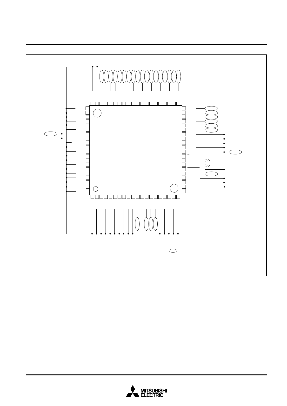
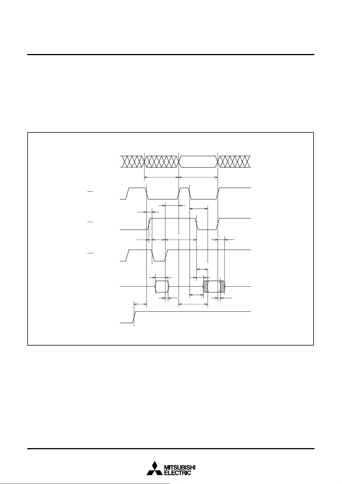
Read-only mode
The microcomputer enters the read-only mode by applying VPPL to
the VPP pin. In this mode, the user can input the address of a
memory location to be read and the control signals at the timing
V
Address Valid address
CE
OE
WE
Data Dout
IH
V
IL
V
IH
V
IL
V
IH
V
IL
V
IH
V
IL
V
OH
V
OL
t
WRR
Floating Floating
shown in Figure 8, and the M37753FFCFP and the M37753FFCHP
will output the contents of the user’s specified address from data I/O
pin to the external. In this mode, the user cannot perform any operation other than read.
t
RC
t
a(CE)
t
DF
t
CLZ
t
t
a(AD)
t
a(OE)
OLZ
t
DH
Fig. 8 Read timing
Read/Write mode
The microcomputer enters the read/write mode by applying VPPH to
the VPP pin. In this mode, the user must first input a software command to choose the operation (e. g., read, program, or erase) to be
performed on the flash memory (this is called the first cycle), and
then input the information necessary for execution of the command
(e.g, address and data) and control signals (this is called the second
Table 3 shows the software commands and the input/output information in the first and the second cycles. The input address is latched
internally at the falling edge of the WE input; software commands
and other input data are latched internally at the rising edge of the
___
WE input.
The following explains each software command. Refer to Figures 9
to 11 for details about the signal input/output timings.
cycle). When this is done, the M37753FFCFP and the
M37753FFCHP execute the specified operation.
Table 3. Software command (Parallel input/output mode)
Symbol
Read
Program
Program verify
Erase
Erase verify
Reset
Device identification
Note: ADI = Device identification address : manufacturer’s code 0000016, device code 0000116
DDI = Device identification data : manufacturer’s code 1C16, device code D016
X can be VIL or VIH.
Address input
×
×
×
×
Verify address
×
×
First cycle
Data input
0016
4016
C016
2016
A016
FF16
9016
Address input
Read address
Program address
×
×
×
×
ADI
___
Second cycle
Data I/O
Read data (Output)
Program data (Input)
Verify data (Output)
2016 (Input)
Verify data (Output)
FF16 (Input)
DDI (Output)
17
Page 18
PRELIMINARY
Notice: This is not a final specification.
Some parametric limits are subject to change.
MITSUBISHI MICROCOMPUTERS
M37753FFCFP
M37753FFCHP
SHINGLE-CHIP 16-BIT CMOS MICROCOMPUTER FLASH MEMORY VERSION
Read command
The microcomputer enters the read mode by inputting command
code “0016” in the first cycle. The command code is latched into the
internal command latch at the rising edge of the WE input. When the
address of a memory location to be read is input in the second cycle,
with control signals input at the timing shown in Figure 9, the
M37753FFCFP and the M37753FFCHP output the contents of the
specified address from the data I/O pins to the external.
Address Valid address
CE
OE
___
V
IH
V
IL
WC
t
V
IH
V
IL
t
CS
V
IH
V
IL
t
t
RRW
WP
The read mode is retained until any other command is latched into
the command latch. Consequently, once the M37753FFCFP and the
M37753FFCHP enter the read mode, the user can read out the successive memory contents simply by changing the input address and
executing the second cycle only. Any command other than the read
command must be input beginning from its command code over
again each time the user execute it. The contents of the command
latch immediately after power-on is 0016.
t
RC
t
CH
t
WRR
t
a(CE)
t
DF
Fig. 9 Timings during reading
WE
Data
V
PP
V
IH
V
IL
V
IH
V
IL
VPPH
PP
V
t
a(OE)
t
DS
t
OLZ
16
t
DH
t
VSC
L
t
a(AD)
t
CLZ
Dout00
t
DH
18
Page 19
PRELIMINARY
Notice: This is not a final specification.
Some parametric limits are subject to change.
MITSUBISHI MICROCOMPUTERS
M37753FFCFP
M37753FFCHP
SHINGLE-CHIP 16-BIT CMOS MICROCOMPUTER FLASH MEMORY VERSION
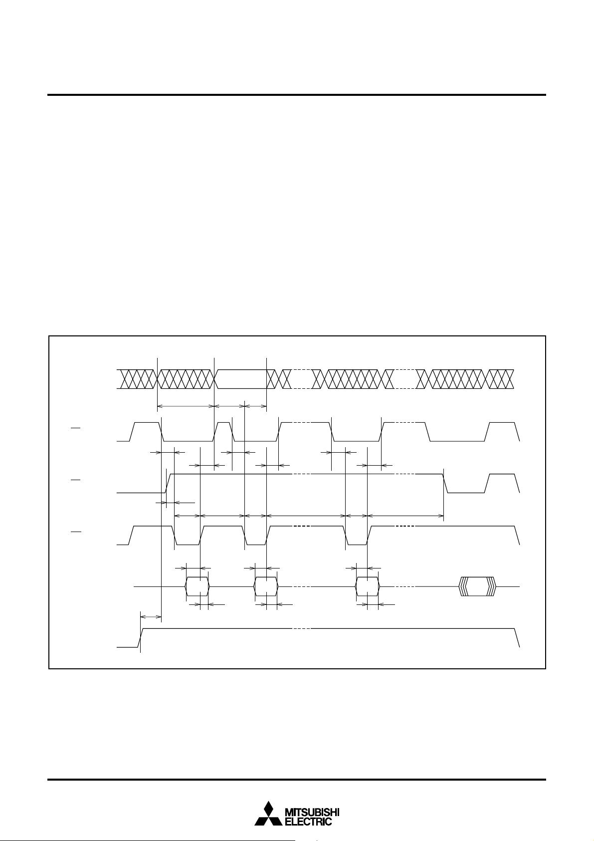
Program command
The microcomputer enters the program mode by inputting command
code “4016” in the first cycle. The command code is latched into the
internal command latch at the rising edge of the WE input. When the
address which indicates a program location and data are input in the
second cycle, the M37753FFCFP and the M37753FFCHP internally
latch the address at the falling edge of the WE input and the data at
___
the rising edge of the WE input. The M37753FFCFP and the
M37753FFCHP start programming at the rising edge of the WE input in the second cycle and finishes programming within 10 µs as
measured by its internal timer. Programming is performed in units of
bytes.
Note: A programming operation is not completed by executing the
program command once. Always be sure to execute a program verify command after executing the program command.
When the failure is found in this verification, the user must repeatedly execute the program command until the pass. Refer
to Figure 12 for the programming flowchart.
V
Address
IH
V
IL
WC
t
___
___
___
Program
address
t
AStAH
Program verify command
The microcomputer enters the program verify mode by inputting
command code “C016” in the first cycle. This command is used to
verify the programmed data after executing the program command.
The command code is latched into the internal command latch at the
rising edge of the WE input. When control signals are input in the
second cycle at the timing shown in Figure 10, the M37753FFCFP
and the M37753FFCHP output the programmed address’s contents
to the external. Since the address is internally latched when the program command is executed, there is no need to input it in the second cycle.
Program
___
Program verify
V
CE
OE
WE
Data
PP
V
V
V
V
V
V
V
V
VPPH
PP
V
IH
IL
IH
IL
IH
IL
IH
IL
L
t
VSC
t
CS
t
t
RRW
t
WP
t
DS
40
16
t
CS
CH
t
WPH
DH
t
t
CH
t
WP
t
DS
D
IN
t
DP
t
DH
t
CS
t
CH
t
WP
t
DS
C0
16
t
WRR
t
DH
Fig. 10 Input/output timings during programming (Verify data is output at the same timing as for read.)
Dout
Verify data output
19
Page 20
PRELIMINARY
Notice: This is not a final specification.
Some parametric limits are subject to change.
MITSUBISHI MICROCOMPUTERS
M37753FFCFP
M37753FFCHP
SHINGLE-CHIP 16-BIT CMOS MICROCOMPUTER FLASH MEMORY VERSION
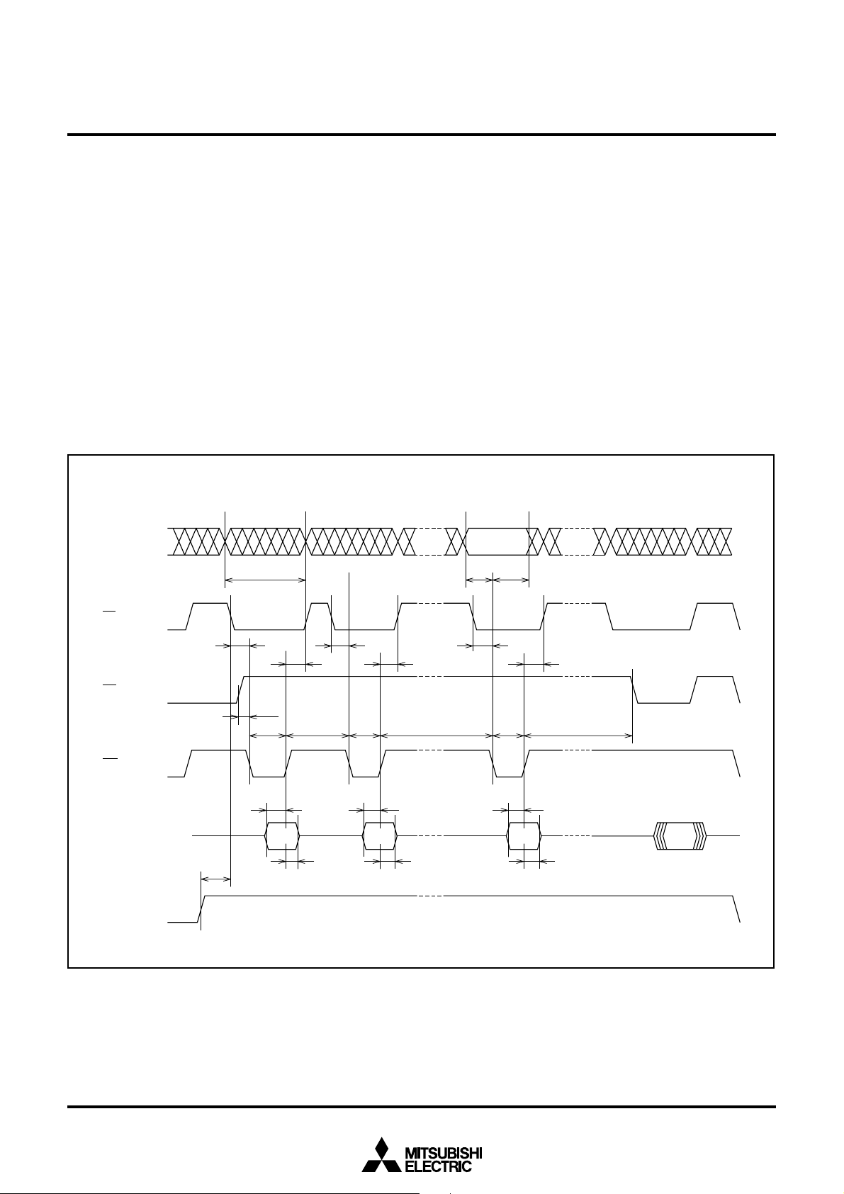
Erase command
The erase command is executed by inputting command code 2016
in the first cycle and command code 2016 again in the second cycle.
The command code is latched into the internal command latch at the
rising edges of the WE input in the first cycle and in the second cycle,
respectively. The erase operation is initiated at the rising edge of the
___
WE input in the second cycle, and the memory contents are collectively erased within 9.5 ms as measured by the internal timer. Note
that data 0016 must be written to all memory locations before executing the erase command.
Note: An erase operation is not completed by executing the erase
command once. Always be sure to execute an erase verify
command after executing the erase command. When the failure is found in this verification, the user must repeatedly execute the erase command until the pass. Refer to Figure 12
for the erase flowchart.
Address
___
V
IH
V
IL
WC
t
Erase verify command
The user must verify the contents of all addresses after completing
the erase command. The microcomputer enters the erase verify
mode by inputting the verify address and command code A016 in the
first cycle. The address is internally latched at the falling edge of the
___
WE input, and the command code is internally latched at the rising
edge of the WE input. When control signals are input in the second
cycle at the timing shown in Figure 11, the M37753FFCFP and the
M37753FFCHP output the contents of the specified address to the
external.
Note: If any memory location where the contents have not been
Erase
___
erased is found in the erase verify operation, execute the operation of “erase → erase verify” over again. In this case,
however, the user does not need to write data 0016 to memory
locations before erasing.
Erase verify
Verify
address
tASt
AH
V
CE
OE
WE
Data
PP
V
V
V
V
V
V
V
V
VPPH
PP
V
IH
IL
IH
IL
IH
IL
IH
IL
L
t
VSC
t
CS
t
CH
t
RRW
t
WP
t
DS
20
16
DH
t
t
WPH
t
CS
t
CH
t
WP
t
DS
20
16
t
DH
t
DE
t
CS
t
CH
t
WP
t
DS
A0
16
t
DH
Fig. 11 Input/output timings during erasing (Verify data is output at the same timing as for read.)
t
WRR
Dout
Verify data output
20
Page 21

PRELIMINARY
Notice: This is not a final specification.
Some parametric limits are subject to change.
Reset command
The reset command provides a means of stopping execution of the
erase or program command safely. If the user inputs command code
FF16 in the second cycle after inputting the erase or program command in the first cycle and again input command code FF16 in the
third cycle, the erase or program command is disabled (i.e., reset),
and the M37753FFCFP and the M37753FFCHP are placed in the
read mode. If the reset command is executed, the contents of the
memory does not change.
Device identification code command
By inputting command code 9016 in the first cycle, the user can read
out the device identification code. The command code is latched into
the internal command latch at the rising edge of the WE input. At this
time, the user can read out manufacture’s code 1C16 (i.e.,
MITSUBISHI) by inputting 000016 to the address input pins in the
second cycle; the user can read out device code D016 (i. e., 1M-bit
flash memory) by inputting 000116.
These command and data codes are input/output at the same timing
as for read.
SHINGLE-CHIP 16-BIT CMOS MICROCOMPUTER FLASH MEMORY VERSION
___
MITSUBISHI MICROCOMPUTERS
M37753FFCFP
M37753FFCHP
21
Page 22

PRELIMINARY
Notice: This is not a final specification.
Some parametric limits are subject to change.
Program Erase
START
CC
= 5 V, VPP = VPPH
V
SHINGLE-CHIP 16-BIT CMOS MICROCOMPUTER FLASH MEMORY VERSION
MITSUBISHI MICROCOMPUTERS
M37753FFCFP
M37753FFCHP
START
CC
= 5 V, VPP = VPPH
V
INC ADRS
ADRS = first location
X = 0
WRITE PROGRAM
COMMAND
WRITE PROGRAM
DATA
DURATION = 10 µs
X = X + 1
WRITE PROGRAM-VERIFY
COMMAND
DURATION = 6 µs
X = 25 ?
NO
FAIL
VERIFY BYTE ? VERIFY BYTE ?
PASS
NO
LAST ADRS ?
WRITE READ COMMAND
PP
V
DEVICE
PASSED
YES
YES
= VPPL
40
D
PASS
YES
16
IN
C0
16
WRITE ERASE-VERIFY
FAIL
FAIL
00
16
INC ADRS
DEVICE
FAILED
NO
WRITE READ COMMAND
ALL
BYTES = 00
PROGRAM
ALL BYTES = 00
ADRS = first location
WRITE ERASE
COMMAND
WRITE ERASE
COMMAND
DURATION = 9.5 ms
COMMAND
DURATION = 6 µs
VERIFY BYTE ? VERIFY BYTE ?
PASS
LAST ADRS ?
NO
X = 0
X = X + 1
X = 1000 ?
NO
YES
16
?
16
20
16
20
16
A0
16
YES
PASS
00
16
FAIL
Fig. 12 Programming/Erasing algorithm flow chart
22
PP
= VPPL
V
DEVICE
PASSED
DEVICE
FAILED
Page 23

MITSUBISHI MICROCOMPUTERS
M37753FFCFP
PRELIMINARY
Notice: This is not a final specification.
Some parametric limits are subject to change.
DC ELECTRICAL CHARACTERISTICS (Ta = 25 °C, VCC = 5 V ± 10 %, unless otherwise noted)
Symbol
ISB1
ISB2
ICC1
ICC2
ICC3
IPP1
IPP2
IPP3
VPPL
VPPH
Note: VIH, VIL, VOH, VOL, IIH, and IIL for the control input, address input, and data input/output pins conform to the standards for microcomputer modes (e.g.,
memory expansion and microprocessor modes).
VCC supply current (at standby)
VCC supply current (at read)
VCC supply current (at program)
VCC supply current (at erase)
VPP supply current (at read)
VPP supply current (at program)
VPP supply current (at erase)
VPP supply voltage (read only)
VPP supply voltage (read/write)
Parameter Test conditions
SHINGLE-CHIP 16-BIT CMOS MICROCOMPUTER FLASH MEMORY VERSION
VCC = 5.5 V, CE = VIH
VCC = 5.5 V,
__
CE = VCC ± 0.2 V
VCC = 5.5 V, CE = VIL,
tRC = 150 ns, IOUT = 0 mA
VPP = VPPH
VPP = VPPH
0≤VPP≤VCC
VCC<VPP≤VCC + 1.0 V
VPP = VPPH
VPP = VPPH
VPP = VPPH
__
__
VCC
11.4 12.0
M37753FFCHP
Limits
Typ.Min.
Max.
100
100
100
VCC + 1.0
12.6
30
30
30
10
30
30
Unit
1
mA
µA
mA
mA
mA
µA
µA
µA
mA
mA
V
V
AC ELECTRICAL CHARACTERISTICS (Ta = 25 °C, VCC = 5 V ± 10 %, unless otherwise noted) Read-only mode
Symbol
tRC
ta(AD)
ta(CE)
ta(OE)
tCLZ
tOLZ
tDF
tDH
tWRR
Read cycle time
Address access time
__
CE access time
__
OE access time
Output enable time (after CE)
Output enable time (after OE)
Output floating time (after OE)
__
__
__
__ __
Output valid time (after CE, OE, address)
Write recovery time (before read)
Parameter
Read/Write mode
Symbol
tWC
tAS
tAH
tDS
tDH
tWRR
tRRW
tCS
tCH
tWP
tWPH
tDP
tDE
tVSC
Note :The read timing in the read/write mode is the same timing as in the read-only mode.
Write cycle time
Address set up time
Address hold time
Data setup time
Data hold time
Write recovery time (before read)
Read recovery time (before write)
__
CE setup time
__
CE hold time
Write pulse width
Write pulse waiting time
Program time
Erase time
VPP setup time
Parameter
Min.
150
Min.
150
60
50
10
20
60
20
10
9.5
0
0
0
6
0
6
0
0
1
Limits
Limits
Max.
150
150
55
35
Max.
Unit
ns
ns
ns
ns
ns
ns
ns
ns
µs
Unit
ns
ns
ns
ns
ns
µs
µs
ns
ns
ns
ns
µs
ms
µs
23
Page 24

PRELIMINARY
Notice: This is not a final specification.
Some parametric limits are subject to change.
MITSUBISHI MICROCOMPUTERS
M37753FFCFP
M37753FFCHP
SHINGLE-CHIP 16-BIT CMOS MICROCOMPUTER FLASH MEMORY VERSION
Flash memory mode 2 (serial I/O mode)
The M37753FFCFP and the M37753FFCHP have a function to serially input/output the software commands, addresses, and data required for operation on the internal flash memory (e. g., read,
program, and erase) using only a few pins. This is called the serial I/
O (input/output) mode. This mode can be selected by driving the
SDA (serial data input/output), SCLK (serial clock input ), and OE
4
P8
P85P86P87P00P01P02P03P04P05P06P07P10P11P12P13P14P15P16P17P20P21P22P2
64
63
65
P8
3
66
P8
2
67
P8
1
68
P8
0
69
V
V
CC
AV
V
AV
REF
V
P7
P7
P7
P7
P7
P7
P7
CC
CC
SS
SS
70
71
72
73
74
7
75
6
76
5
77
4
78
3
79
2
80
1
626160595857565554535251504948474645444342
1
2
3
4
5
6
7
0
P7
7
P6
6
P6
5
P6
4
P6
3
P6
2
P6
8
1
P6
__
M37753FFCFP
9
10
11
12
0
7
6
5
P6
P5
P5
P5
pins high after connecting wires as shown in Figures 13, 14 and
powering on the VCC pin and then applying VPPH to the VPP pin.
In the serial I/O mode, the user can use seven types of software
commands: bank (0, 1) select, read, program, program verify, auto
erase, and error check.
Serial input/output is accomplished synchronously with the clock,
beginning from the LSB (LSB first).
3
41
40
P2
4
39
P2
5
38
P2
6
37
P2
7
36
P3
0
35
P3
1
34
P3
2
33
P3
3
32
V
SS
31
E
30
X
13
4
P5
14
3
P5
15
2
P5
16
1
P5
17
0
P5
18
7
P4
19
6
P4
20
5
P4
21
4
P4
22
3
P4
23
2
P4
24
1
P4
29
28
27
26
25
OUT
X
IN
RESET
CNV
SS
BYTE
P4
0
✽✽
✽
V
PP
V
SS
Outline 80P6N-A
Fig. 13 Pin connection of M37753FFCFP when operating in serial I/O mode
OE
SDA
SCLK
BUSY
✽ : Connect to the ceramic oscillation circuit.
✽✽ : Connect the BYTE pin to V
indicates the flash memory pin.
CC
or VSS.
24
Page 25

PRELIMINARY
Notice: This is not a final specification.
Some parametric limits are subject to change.
MITSUBISHI MICROCOMPUTERS
M37753FFCFP
M37753FFCHP
SHINGLE-CHIP 16-BIT CMOS MICROCOMPUTER FLASH MEMORY VERSION
P86P87P00P01P02P03P04P05P06P07P10P11P12P13P14P15P16P17P20P2
1
60595857565554535251504948474645444342
61
P8
5
62
P8
4
P8
3
63
64
P8
2
P8
1
65
P8
0
66
V
V
CC
AV
V
AV
REF
V
P7
P7
P7
P7
P7
P7
P7
P7
P6
CC
CC
SS
SS
67
68
69
70
71
7
72
6
73
5
74
4
75
3
76
2
77
1
78
79
0
80
7
1
2
3
6
5
4
P6
P6
P6
M37753FFCHP
4
5
6
2
P6
1
P6
7
0
P6
3
P6
8
7
P5
9
6
P5
10
5
P5
11
4
P5
12
3
P5
13
2
P5
14
1
P5
OE
15
0
P5
16
7
P4
17
6
P4
SCLK
18
5
P4
SDA
41
19
20
3
P44P4
BUSY
40
39
38
37
36
35
34
33
32
31
30
29
28
27
26
25
24
23
22
21
P2
2
P2
3
P2
4
P2
5
P2
6
P2
7
P3
0
P3
1
P3
2
P3
3
V
SS
E
X
OUT
X
IN
RESET
CNV
SS
BYTE
P4
0
P4
1
P4
2
✽✽
V
SS
✽
V
PP
Outline 80P6Q-A
Fig. 14 Pin connection of M37753FFCHP when operating in serial I/O mode
: Connect to the ceramic oscillation circuit.
✽
: Connect the BYTE pin to V
✽✽
CC
or VSS.
indicates the flash memory pin.
25
Page 26

PRELIMINARY
Notice: This is not a final specification.
Some parametric limits are subject to change.
MITSUBISHI MICROCOMPUTERS
M37753FFCFP
M37753FFCHP
SHINGLE-CHIP 16-BIT CMOS MICROCOMPUTER FLASH MEMORY VERSION
Functional outline (Serial I/O mode)
In the serial I/O mode, data is transferred synchronously with the
clock using serial input/output. The input data is read from the SDA
pin into the internal circuit synchronously with the rising edge of the
serial clock pulse; the output data is output from the SDA pin synchronously with the falling edge of the serial clock pulse. Data is
Table 4. Software command (Serial I/O mode)
Number of transfers
Command
Bank 0 select
Bank 1 select
Read
Program
Program verify
Auto erase
Error check
First command
code input
E016
E116
0016
4016
C016
3016
8016
Second
—————
—————
Read address L (Input)
Program address L (Input)
Verify data (Output)
3016 (Input)
Error code (Output)
Bank select command
This is the command which specifies the bank of the flash memory,
which is to be read/programmed, before executing the read command or the program command (and the program verify command).
There are the bank 0 select command (command code “E016”),
which selects bank 0 (addresses 0000016 to 0FFFF16), and the bank
1 select command (command code “E116”), which selects bank 1
(addresses 1000016 to 1FFFF16).
When any bank select command is input once, specified bank is
transferred in units of eight bits.
In the first transfer, the user inputs the command code. This is followed by address input and data input/output according to the contents of the command. Table 4 shows the software commands used
in the serial I/O mode. The following explains each software command.
Third Fourth
—————
—————
Read address H (Input)
Program address H (Input)
—————
—————
—————
valid until the next bank select command is input. Accordingly, when
the read command or the program command (and the program verify
command) is executed to plural bytes in the same bank, if any bank
select command is input first, it is unnecessary to input the bank select command again for the following bytes. When selecting the serial I/O mode (before bank command input), bank 0 is selected.
Note: Bank select command does not affect the auto erase com-
mand, that is to say, when executing the auto erase command, all flash memory is erased collectively regardless of
specified bank.
And in the same way, the bank select command does not affect the error check command.
Read data (Output)
Program data (Input)
—————
—————
—————
—————
—————
SCLK SCLK
SDA
Command code input (E016)
OE
BUSY
Bank 0 select command Bank 1 select command
Fig. 15 Timings during bank select
26
“H”
“L”
00000111
CH
t
SDA
OE
BUSY
10000111
Command code input (E116)
“H”
“L”
t
CH
Page 27

PRELIMINARY
Notice: This is not a final specification.
Some parametric limits are subject to change.
MITSUBISHI MICROCOMPUTERS
M37753FFCFP
M37753FFCHP
SHINGLE-CHIP 16-BIT CMOS MICROCOMPUTER FLASH MEMORY VERSION
Read command
Input command code 0016 in the first transfer . Proceed and input the
low-order 8 bits and the high-order 8 bits of the address and pull the
__
OE pin low. When this is done, the M37753FFCFP and the
M37753FFCHP read out the contents of the specified address, and
t
SCLK
SDA
OE
“L”
BUSY
Note : When outputting the read data, the SDA pin is switched for output at the first falling edge of SCLK. The SDA pin is placed
00000000
Command code input (0016) Read address input (L) Read address input (H) Read data output
in the floating state during the period of th
Fig. 16 Timings during reading
CH
A
0
(C-E)
t
CH
A
7
after the last rising edge of SCLK (at the 8th bit).
then latch it into the internal data latch. When the OE pin is released
__
back high and serial clock is input to the SCLK pin, the read data that
has been latched into the data latch is serially output from the SDA
pin.
A
8
A
15
t
t
CR
WR
Read
D
0
t
RC
D
7
27
Page 28

PRELIMINARY
Notice: This is not a final specification.
Some parametric limits are subject to change.
MITSUBISHI MICROCOMPUTERS
M37753FFCFP
M37753FFCHP
SHINGLE-CHIP 16-BIT CMOS MICROCOMPUTER FLASH MEMORY VERSION
Program command
Input command code 4016 in the first transfer . Proceed and input the
low-order 8 bits and the high-order 8 bits of the address and then
program data. Programming is initiated at the last rising edge of the
serial clock during program data transfer. The BUSY pin is driven
high during program operation. Programming is completed within 10
µs as measured by the built-in timer , and the B USY pin is pulled lo w.
SCLK
SDA
OE
BUSY
00000010
Command code input (4016) Program address input (L) Program address input (H)
Fig. 17 Timings during programming
CH
t
A
0
A
t
CH
7
Note :A programming operation is not completed by executing the
program command once. Always be sure to execute a program verify command after executing the program command.
In the case of failure in the verification, the user must repeatedly execute the program command until the pass in the verification. Refer to Figure 12 for the programming flowchart.
t
CH
t
A
D
8
A
15
0
Program data input
D
7
WP
t
Program
PC
Program verify command
Input command code C016 in the first transfer . Proceed and drive the
__
OE pin low. When this is done, the M37753FFCFP and the
M37753FFCHP verify-read the programmed address’s contents,
SCLK
SDA
OE
BUSY
Note: When outputting the verify data, the SDA pin is switched for output at the first falling edge of SCLK. The SDA pin is placed
in the floating state during the period of th
Fig. 18 Timings during program verify
“L”
00000011
Command code input (C016) Verify data output
(C-E)
after the last rising edge of SCLK (at the 8th bit).
and then latch it into the internal data latch. When the OE pin is released back high and serial clock is input to the SCLK pin, the verify
data that has been latched into the data latch is serially output from
the SDA pin.
t
CRPV
t
WR
Verify read
0
D
t
RC
D
7
__
28
Page 29

PRELIMINARY
Notice: This is not a final specification.
Some parametric limits are subject to change.
MITSUBISHI MICROCOMPUTERS
M37753FFCFP
M37753FFCHP
SHINGLE-CHIP 16-BIT CMOS MICROCOMPUTER FLASH MEMORY VERSION
Auto erase command
Input command code 3016 in the first transfer and command code
3016 again in the second transfer. When this is done, the
M37753FFCFP and the M37753FFCHP execute an auto erase command. A uto erase is initiated at the last rising edge of the serial clock.
The BUSY pin is driven high during the auto erase operation. Auto
CH
t
SCLK
SDA
“H”
OE
BUSY
Fig. 19 Timings at auto-erasing
00001100 00001100
Command code input (30
16
) Command code input (3016)
erase is completed when all memory contents are erased, and the
BUSY pin is pulled low.
Note: In the auto erase operation, the M37753FFCFP and the
M37753FFCHP automatically repeat the erase and verify operations internally. Therefore, erase is completed by executing the command once.
t
EC
Auto-erase
Error check command
Input command code 8016 in the first transfer, and the
M37753FFCFP and the M37753FFCHP output error information
from the SDA pin, beginning at the next falling edge of the serial
clock. If the E0 of the 8-bit error information is 1, it indicates that a
command error has occurred. A command error means that some invalid commands other than commands shown in Table 4 has been
input.
When a command error occurs, the serial communication circuit sets
the corresponding flag and stops functioning to avoid an erroneous
programming or erase. When being placed in this state, the serial
communication circuit does not accept the subsequent serial clock
and data (even including an error check command). Therefore, if the
SCLK
SDA
OE
BUSY
“H”
“L”
00000001
Command code input (8016) Error flag output
user wants to execute an error chec k command, temporarily drop the
VPP pin input to the VPPL level to terminate the serial input/output
mode. Then, place the M37753FFCFP and the M37753FFCHP into
the serial I/O mode back again. The serial communication circuit is
reset by this operation and is ready to accept commands. The error
flag alone is not cleared by this operation, so the user can examine
the serial communication circuit’s error conditions before reset. This
examination is done by the first execution of an error check command after the reset. The error flag is cleared when the user has executed the error check command. Because the error flag is
undefined immediately after power-on, always be sure to e x ecute the
error check command.
t
CH
E0
??????
?
Note: When outputting the error flag, the SDA pin is switched for output at the first falling edge of the serial clock. The SDA pin is placed
in the floating state during the period of th
Fig. 20 Timings at error checking
(C-E)
after the last rising edge of the serial clock (at the 8th bit).
29
Page 30

MITSUBISHI MICROCOMPUTERS
M37753FFCFP
PRELIMINARY
Notice: This is not a final specification.
Some parametric limits are subject to change.
DC ELECTRICAL CHARACTERISTICS (Ta = 25 °C, VCC = 5 V ± 10 %, VPP = 12 V ± 5 %, unless otherwise noted)
ICC, IPP-relevant standards during read, program, and erase are the same as in the parallel input/output mode. VIH, VIL, VOH, VOL, IIH, and IIL for
the SCLK, SDA, BUSY, OE pins conform to the microcomputer modes.
__
AC ELECTRICAL CHARACTERISTICS
(Ta = 25 °C, VCC = 5 V ± 10 %, VPP = 12 V ± 5 %, f(XIN) = 40 MHz, unless otherwise noted)
Symbol
tCH
tCR
tWR
tRC
tCRPV
tWP
tPC
tEC
tc(CK)
tw(CKH)
tw(CKL)
tr(CK)
tf(CK)
td(C-Q)
th(C-Q)
th(C-E)
tsu(D-C)
th(C-D)
Notes 1: When f(XIN) = 25 MHz or less, calculate the minimum value according to formula 1.
2: When f(XIN) = 25 MHz or less, calculate the minimum value according to formula 2.
3: When f(XIN) = 25 MHz or less, calculate the minimum value according to formula 3.
4: When f(XIN) = 25 MHz or less, calculate the minimum value according to formula 4
Serial transmission interval
Read waiting time after transmission
Read pulse width
Transfer waiting time after read
Waiting time before program verify
Programming time
Transfer waiting time after programming
Transfer waiting time after erase
SCLK input cycle time
SCLK high-level pulse width
SCLK low-level pulse width
SCLK rise time
SCLK fall time
SDA output delay time
SDA output hold time
SDA output hold time (only the 8th bit)
SDA input set up time
SDA input hold time
Formula 1 : × 10
Formula 2 : × 10
Formula 3 : × 10
Formula 4 : × 10
1 × 10
f(X
1 × 8
f(X
1 × 3
f(X
1 × 5
f(X
9
IN)
9
IN)
9
IN)
9
IN)
SHINGLE-CHIP 16-BIT CMOS MICROCOMPUTER FLASH MEMORY VERSION
Parameter
M37753FFCHP
400
400
320
400
400
400
120
Min.
(Note 1)
(Note 1)
(Note 2)
(Note 1)
6
(Note 1)
(Note 1)
250
100
100
20
20
0
0
(Note 3)
30
90
Limits
200
Max.
10
90
(Note 4)
Unit
ns
ns
ns
ns
µs
µs
ns
ns
ns
ns
ns
ns
ns
ns
ns
ns
ns
ns
AC waveforms
SCLK
SDA output
SDA input
30
t
f(CK)
t
d(C-Q)
t
w(CKL)
c(CK)
t
t
r(CK)
t
su(D-C)th(C-D)
t
w(CKH)
t
h(C-E)
t
h(C-Q)
Test conditions for AC characteristics
• Output timing voltage : V
• Input timing voltage : V
OL
= 0.8 V, VOH = 2.0 V
IL
= 0.2 VCC, VIH = 0.8 V
CC
Page 31

PRELIMINARY
Notice: This is not a final specification.
Some parametric limits are subject to change.
MITSUBISHI MICROCOMPUTERS
M37753FFCFP
M37753FFCHP
SHINGLE-CHIP 16-BIT CMOS MICROCOMPUTER FLASH MEMORY VERSION
Flash memory mode 3 (CPU reprogramming mode)
The M37753FFCFP and the M37753FFCHP have the CPU reprogramming mode where a built-in flash memory is handled by the central processing unit (CPU). 112 Kbytes (addresses 00100016 to
00EFFF16 and addresses 01100016 to 01EFFF16) of the 120-Kbyte
flash memory shown in Figure 1 can be reprogrammed (erase and
program). Remaining 8 Kbytes of the flash memory (addresses
00F00016 to 010FFF16) cannot be reprogrammed, but can be read.
(It is possible to reprogram this remaining 8 Kbytes in the parallel I/O
mode and the serial I/O mode). This area of 8 Kbytes can be used as
an area where the control program of CPU reprogramming mode is
stored.
In CPU reprogramming mode, the flash memory is handled by writing and reading to/from the flash memory control register (see Figure 21) and the flash command register (see Figure 22).
The CNVSS pin is used as the VPP power supply pin in CPU reprogramming mode. It is necessary to apply the power-supply voltage of
VPPH from the external to this pin.
Functional outline (Parallel input/output mode)
Figure 21 shows the flash memory control register bit configuration.
Figure 22 shows the flash command register bit configuration.
Bit 0 of the flash memory control register is the CPU reprogramming
mode select bit. When this bit is set to “1” and VPPH is applied to the
CNVss/VPP pin, the CPU reprogramming mode is selected. Whether
the CPU reprogramming mode is realized or not is judged by reading
the CPU reprogramming mode monitor flag (bit 3 of the flash
memory control register).
Bit 1 is a busy flag which becomes “1" during auto erase, erase, and
program execution.
Whether these operations have been completed or not is judged by
checking this flag after each command of auto erase, erase, and the
program is executed.
Bits 4, 5 of the flash memory control register are the erase/program
area select bits. These bits specify an area where auto erase, erase,
and program is operated. When the auto erase and the erase commands are executed after an area is specified by these bits, only the
specified area is erased. Only for the specified area, programming is
enabled; for the other areas, programming is disabled.
Figure 23 shows the processor mode register 0 bit configuration in
the CPU reprogramming mode. Set bit 1 to “0” (single-chip or
memory expansion mode) in the CPU reprogramming mode. Set bit
2 (internal memory access bus cycle select bit) to “0.”
Be sure to set data length select flag m to “1" (8-bit length) beforehand because writing and reading of data are operated in unit of
byte.
76543210
00
Notes 1: Bit 0 can be reprogrammed only when 0 V is applied to the CNV
2: When bit 0 is “1,” the processor mode does not change even if V
Flash memory control regsiter
Fig. 21 Flash memory control register bit configuration
Address
67
16
CPU reprogramming mode select bit (Notes 1, 2)
0 : CPU reprogramming mdoe is invalid. (Normal operation mode)
1 : When applying 0 V or V
invalid. When applying V
Auto erase/Erase/Program busy flag
0 : Auto erase, erase, and program are completed or not have been executed.
1 : Auto erase/erase/program is being executed.
CPU reprogramming mode monitor flag
0 : CPU reprogramming mode is invalid.
1 : CPU reprogramming mode is valid.
Fix this bit to “0.”
Erase/Program area select bits
0 ✕ : Addresses 001000
and addresses 011000
1 0 : Addresses 001000
1 1 : Addresses 011000
Fix this bit to “0.”
PP
PP
16
to 00EFFF16
16
16
to 00EFFF16 (total 56 Kbytes)
16
to 01EFFF16 (total 56 Kbytes)
SS/VPP
PP
L to CNVSS/VPP pin, CPU reprogramming mode is
H to CNVSS/VPP pin, CPU reprogramming mode is valid.
to 01EFFF16 (total 112 Kbytes)
pin.
H is applied to the CNVSS/VPP pin.
31
Page 32

PRELIMINARY
Notice: This is not a final specification.
Some parametric limits are subject to change.
MITSUBISHI MICROCOMPUTERS
M37753FFCFP
M37753FFCHP
SHINGLE-CHIP 16-BIT CMOS MICROCOMPUTER FLASH MEMORY VERSION
CPU reprogramming mode operation procedure
The operation procedure in CPU reprogramming mode is described
below.
< Beginning procedure >
➀ Apply 0 V to the CNVss/VPP pin for reset release.
➁ Set the processor mode register 0 (see Figure 23).
➂ After CPU reprogramming mode control program is transferred to
internal RAM, jump to this control program on RAM. (The following operations are controlled by this control program).
➃ Set “1" (8-bit length) to data length select flag m.
➄ Set “1" to the CPU reprogramming mode select bit.
➅ Apply VPPH to the CNVSS/VPP pin.
➆ Read the CPU reprogramming mode monitor flag to confirm
whether the CPU reprogramming mode is valid.
➇ The operation of the flash memory is executed by software-com-
mand-writing to the flash command register .
Note: The following are necessary other than this:
•Control for data which is input from the external (serial I/O
etc.) and to be programmed to the flash memory
•Initial setting for ports etc.
•Writing to the watchdog timer
< Release procedure >
➀ Apply 0V to the CNVSS/VPP pin.
➁ Set the CPU reprogramming mode select bit to “0.”
Each software command is explained as follows.
Read command
When “0016" is written to the flash command register, the
M37753FFCFP and the M37753FFCHP enter the read mode. The
contents of the corresponding address can be read by reading the
flash memory (For instance, with the LDA instruction etc.) under this
condition.
The read mode is maintained until another command code is written
to the flash command register. Accordingly, after setting the read
mode once, the contents of the flash memory can continuously be
read.
After reset and after the reset command is executed, the read mode
is set.
76543 210
Flash command register
Writing of software command
<Software command name>
• Read command
• Program command
• Program verify command
• Erase command
• Erase verify command
• Auto erase command
• Reset command
Note: The flash command register is write-only register.
<Command code>
“00
“40
“C0
“20
“A0
“30
“FF
Fig. 22 Flash command register bit configuration
16
”
16
”
16
”
16
” + “2016”
16
”
16
” + “3016”
16
” + “FF16”
Address
16
65
76543 21 0
000
Note: For the description of processor mode register 0, refer to Figure 14
on the M37754M8C-XXXGP data sheet.
Processor mode register 0
Processor mode bits
0 0 : Single-chip mode
0 1 : Memory expansion mode
1 ✕ : Do not select.
Internal memory access bus cycle select bit
Fix this bit to “0.”
Software reset bit
Interrupt priority detection time select bits
Test mode bit
Fix this bit to “0.”
1
output select bit
Clock φ
Address
5E
16
Fig. 23 Processor mode register 0 bit configuration in CPU rewrit-
ing mode
32
Page 33

PRELIMINARY
Notice: This is not a final specification.
Some parametric limits are subject to change.
MITSUBISHI MICROCOMPUTERS
M37753FFCFP
M37753FFCHP
SHINGLE-CHIP 16-BIT CMOS MICROCOMPUTER FLASH MEMORY VERSION
Program command
When “4016" is written to the flash command register, the
M37753FFCFP and the M37753FFCHP enter the program mode.
Subsequently to this, if the instruction (for instance, STA or LDM instruction) for writing byte data in the address to be programmed is
executed, the control circuit of the flash memory executes the program. The auto erase/erase/program busy flag of the flash memory
control register is set to “1" when the program starts, and becomes
“0" when the program is completed. Accordingly, after the write instruction is executed, CPU can recognize the completion of the program by polling this bit.
The programmed area must be specified beforehand by the erase/
program area select bits.
During programming, watchdog timer stops with “FFF16” set.
Note: A programming operation is not completed by executing the
program command once. Always be sure to execute a program verify command after executing the program command.
When the failure is found in this verification, the user must repeatedly execute the program command until the pass. Refer
to Figure 24 for the flow chart of the programming.
Program verify command
When “C016" is written to the flash command register, the
M37753FFCFP and the M37753FFCHP enter the program verify
mode. Subsequently to this, if the instruction (for instance, LDA instruction) for reading byte data from the address to be verified (i.e.,
previously programmed address), the contents which has been written to the address actually is read.
CPU compares this read data with data which has been written by
the previous program command. In consequence of the comparison,
if not agreeing, the operation of “program → program verify” must be
executed again.
Erase command
When writing “2016” twice continuously to the flash command register, the flash memory control circuit performs erase to the area specified beforehand by the erase/program area select bits.
Auto erase/erase/program busy flag of the flash memory control register becomes “1" when erase begins, and it becomes “0" when
erase completes. Accordingly, CPU can recognize the completion of
erase by polling this bit.
Data “0016” must be written to all areas to be erased by the program
and the program verify commands before the erase command is executed.
During programming, watchdog timer stops with “FFF16” set.
Note: The erasing operation is not completed b y e xecuting the erase
command once. Always be sure to execute an erase verify
command after executing the erase command. When the failure is found in this verification, the user must repeatedly execute the erase command until the pass. Refer to Figure 24 for
the erasing flowchart.
Erase verify command
When “A016" is written to the flash command register, the
M37753FFCFP and the M37753FFCHP enter the erase verify mode.
Subsequently to this, if the instruction (for instance, LDA instruction)
for reading byte data from the address to be v erified, the contents of
the address is read.
CPU must erase and verify to all erased areas in a unit of address.
If the address of which data is not “FF16" (i.e., data is not erased) is
found, it is necessary to discontinue erasure verification there, and
execute the operation of “erase → erase verify” again.
Note: By executing the operation of “erase →erase verify” again
when the memory not erased is found. It is unnecessary to
write data “0016” before erasing in this case.
33
Page 34

PRELIMINARY
Notice: This is not a final specification.
Some parametric limits are subject to change.
Program Erase
START
SHINGLE-CHIP 16-BIT CMOS MICROCOMPUTER FLASH MEMORY VERSION
MITSUBISHI MICROCOMPUTERS
M37753FFCFP
M37753FFCHP
START
ADRS = first location
X = 0
WRITE PROGRAM
COMMAND
WRITE PROGRAM
DATA
NOP ✕ 10
NO
ERASE PROGRAM
BUSY FLAG = 0
X = X + 1
WRITE PROGRAM-VERIFY
COMMAND
DURATION = 6 µs
X = 25 ?
NO
FAIL
VERIFY BYTE ? VERIFY BYTE ?
YES
YES
PASS
40
DIN
YES
16
16
C0
NO
ALL
BYTES = 00
ALL BYTES = 00
ADRS = first location
WRITE ERASE
COMMAND
WRITE ERASE
COMMAND
ERASE PROGRAM
BUSY FLAG = 0
WRITE ERASE-VERIFY
COMMAND
DURATION = 6 µs
NO
PROGRAM
X = 0
NOP ✕ 10
YES
X = X + 1
16
?
16
16
20
20
16
A0
16
INC ADRS
PASS
NO
LAST ADRS ?
YES
WRITE READ COMMAND
DEVICE
PASSED
00
FAIL
16
DEVICE
FAILED
Fig. 24 Flowchart when program/erase/auto erase is executed (1)
INC ADRS
X = 1000 ?
NO
FAIL
VERIFY BYTE ? VERIFY BYTE ?
PASS
NO
LAST ADRS ?
WRITE READ COMMAND
YES
DEVICE
PASSED
YES
PASS
00
FAIL
16
DEVICE
FAILED
34
Page 35

PRELIMINARY
Notice: This is not a final specification.
Some parametric limits are subject to change.
MITSUBISHI MICROCOMPUTERS
M37753FFCFP
M37753FFCHP
SHINGLE-CHIP 16-BIT CMOS MICROCOMPUTER FLASH MEMORY VERSION
Auto erase command
When writing “3016” twice continuously to the flash command register, the flash memory control circuit executes the auto erase sequence described below for the area specified beforehand by the
erase/program area select bits.
(1) Data “0016" is written to the area to be erased in the flash
memory.
(2) The erasure is executed.
(3) The contents of the erased flash memory is erase-verified one by
one. When the address which is not erased is found, verification
is interrupted, and after the erase command is executed again,
erase-verification is operated again.
(4) When the erasure of all areas specified to be erased, is con-
firmed by erase-verify-operation, the auto erase command is
ended.
The auto erase/erase/program busy flag of the flash memory control
register becomes “1" when auto erase starts, and becomes “0" when
auto erase completes. Accordingly, CPU can recognize the completion of auto erase by polling this bit.
During auto erase, watchdog timer stops with “FF16” set.
Note: When the flash memory is erased by using the auto erase
command, it is unnecessary to execute the erase and erase
verify commands. Figure 25 shows the flowchart when auto
erase is executed.
DC electric characteristics
Note: The characteristic of the flash memory part are the same as
the standard of the parallel I/O mode.
AC electric characteristics
Note: The characteristics are the same as the standards of the mi-
crocomputer mode.
Reset command
The reset command is a command to discontinue the program,
erase, or the auto erase command on the way. When “FF16” is written to the command register two times continuously after “4016,”
“2016,” or “3016” is written to the flash command register, the pro-
gram, erase, or auto erase command becomes invalid (reset), and
the M37753FFCFP and the M37753FFCHP enters the reset mode.
The contents of the memory does not change even if the reset command is executed.
Auto erase
START
WRITE AUTO-ERASE
COMMAND
WRITE AUTO-ERASE
COMMAND
NO
ERASE PROGRAM
BUSY FLAG = 0
NOP ✕ 10
YES
DEVICE
PASSED
30
16
30
16
Fig. 25 Flowchart when program/erase/auto erase is executed (2)
35
Page 36

PRELIMINARY
Notice: This is not a final specification.
Some parametric limits are subject to change.
ABSOLUTE MAXIMUM RATINGS
Symbol
VCC
AVCC
VI
VI
VO
Pd
Topr
Tstg
Note : For the CNVSS pin, this is 12.6V when programming to the flash memory.
Power source voltage
Analog power source voltage
Input voltage RESET, CNVSS, BYTE
Input voltage P00–P07, P10–P17, P20–P27, P30–P33, P40–P47,
P50–P57, P60–P67, P70–P77, P80–P87,
VREF, XIN
Output voltage P00–P07, P10–P17, P20–P27, P30–P33, P40–P47,
P50–P57, P60–P67, P70–P77, P80–P87,
XOUT, E
Power dissipation
Operating temperature
Storage temerature
SHINGLE-CHIP 16-BIT CMOS MICROCOMPUTER FLASH MEMORY VERSION
Parameter
MITSUBISHI MICROCOMPUTERS
M37753FFCFP
M37753FFCHP
Ratings
–0.3 to 7
–0.3 to 7
–0.3 to 12 (Note)
–0.3 to VCC+0.3
–0.3 to VCC+0.3
300
–20 to 85
–40 to 150
Unit
V
V
V
V
V
mW
°C
°C
RECOMMENDED OPERATING CONDITIONS
Symbol
VCC
AVCC
VSS
AVSS
VIH
VIH
VIH
VIL
VIL
VIL
IOH(peak)
IOH(avg)
IOL(peak)
IOL(peak)
IOL(avg)
IOL(avg)
f(XIN)
Notes 1: Average output current is the averaage value of a 100 ms interval.
Supply voltage
Analog supply voltage
Supply voltage
Analog supply voltage
High-level input voltage P00–P07, P30–P33, P40–P47,
P50–P57, P60–P67, P70–P77, P80–P87, XIN,
RESET, CNVSS, BYTE
High-level input voltage P10–P17, P20–P27 (in single-chip mode)
High-level input voltage P10–P17, P20–P27
(in memory expansion mode and microprocessor mode)
Low-level input voltage P00–P07, P30–P33, P40–P47,
P50–P57, P60–P67, P70–P77, P80–P87, XIN,
RESET, CNVSS, BYTE
Low-level input voltage P10–P17, P20–P27 (in single-chip mode)
Low-level input voltage P10–P17, P20–P27
(in memory expansion mode and microprocessor mode)
High-level peak output current P00–
High-level average output current P00–
Low-level peak output current P00–
Low-level peak output current
Low-level average output current P00–
Low-level average output current
External clock frequency input (Note 3)
2: The sum of IOL(peak) for ports P0, P1, P2, P3, and P8 must be 80 mA or less, the sum of IOH(peak) for ports P0, P1, P2, P3, and P8 must
be 80 mA or less, the sum of IOL(peak) for ports P4, P5, P6, and P7 must be 110 mA or less, the sum of IOH(peak) for ports P4, P5, P6,
and P7 must be 80 mA or less.
3: When the clock source select bit is “1,” f(XIN)’s maximum limit is 12.5 MHz at low-speed running and is 20 MHz at high-speed
running.
P07, P10–
P50–
P57, P60–
P50–
P07, P10–
P56,
P57, P60–
P50–P55
P56,
P50–P55
Parameter
P07, P10–
P57, P60–
P07, P10–
P57, P60–
Low-speed running
High-speed running
(Vcc = 5 V±10 %, Ta = –20 to 85 °C, unless otherwise noted)
Min.
4.5
0.8 VCC
0.8 VCC
0.5 VCC
0
0
0
P17, P20–
P67, P70–
P17, P20–
P67, P70–
P27, P30–
P77, P80–
P17, P20–
P67, P70–
P27, P30–
P77, P80–
P17, P20–
P67, P70–
P33, P40–
P8
P27, P30–
P77, P80–
P33, P40–
P8
P27, P30–
P77, P80–
P47,
7
P33, P40–
P8
7
7
P33, P40–
P8
7
P47,
P47,
P47,
Limits
Typ.
5.0
VCC
0
0
0.2 VCC
0.2 VCC
0.16 VCC
Max.
5.5
VCC
VCC
VCC
–10
–5
10
20
5
15
25
40
Unit
V
V
V
V
V
V
V
V
V
V
mA
mA
mA
mA
mA
mA
MHz
36
Page 37

MITSUBISHI MICROCOMPUTERS
M37753FFCFP
PRELIMINARY
Notice: This is not a final specification.
Some parametric limits are subject to change.
ELECTRICAL CHARACTERISTICS (Vcc = 5 V, V ss = 0 V, Ta = –20 to 85 °C, f(XIN) = 40 MHz (Note))
Symbol
High-level output voltage
VOH
VOH
VOH
VOH
VOL
VOL
VOL
VOL
VT+ —VT–
VT+ —VT–
VT+ —VT–
IIH
IIL
IIL
VRAM
ICC
Note: f(XIN) = 20 MHz when the clock source select bit = “1.”
High-level output voltage
High-level output voltage P32
High-level output voltage E
Low-level output voltage
Low-level output voltage
Low-level output voltage
Low-level output voltage E
Low-level output voltage
Hysteresis HOLD, RDY, TA0IN–TA4IN,
Hysteresis RESET, HOLD, RDY
Hysteresis XIN
High-level input current
Low-level input current
Low-level input current P54–P57, P80
RAM hold voltage
Power supply current (target value)
Parameter
TB0IN–TB2IN, INT0–INT4, ADTRG,
CTS0, CTS1, CLK0, CLK1, RxD0,
RxD1
SHINGLE-CHIP 16-BIT CMOS MICROCOMPUTER FLASH MEMORY VERSION
Test conditions
P00–P07, P10–P17, P20–P27,
P30, P31, P33, P40–P47,
P50–P57, P60–P67, P70–P77,
P80–P8
7
P00–P07, P10–P17, P20–P27,
P30, P31, P33,
P00–P07, P10–P17, P20–P27,
P30, P31, P33, P40–P47,
P56, P57, P60–P67,P70–P77,
P80–P8
7
P00–P07, P10–P17, P20–P27,
P30, P31, P3
P3
P50–P5
P00–P07, P10–P17, P20–P27,
P30–P33, P40–P47, P50–P57,
P60–P67, P70–P77, P80–P87,
XIN, RESET , CNVSS, BYTE
P00–P07, P10–P17, P20–P27,
P30–P33, P40–P47, P50–P53,
P60–P67, P70–P77, P81–P87,
XIN, RESET, CNVSS, BYTE
3
2
5
IOH = –10 mA
IOH = –400 µA
IOH = –10 mA
IOH = –400 µA
IOH = –10 mA
IOH = –400 µA
IOL = 10 mA
IOL = 2 mA
IOL = 10 mA
IOL = 2 mA
IOL = 10 mA
IOL = 2 mA
IOL = 20 mA
IOL = 2 mA
VI = 5 V
VI = 0 V
VI = 0 V, No pull-up transistor
VI = 0 V, Pull-up transistor used
When clock is stoped.
Output-only pin is
open and other
pins are Vss during
reset.
f(XIN) = 40 MHz, square
waveform (Note)
Ta = 25 °C when clcock
is stopped.
Ta = 85 °C when clcock
is stopped.
M37753FFCHP
Min.
3
4.7
3.1
4.8
3.4
4.8
0.4
0.2
0.1
–0.25
2
Limits
Typ.
–0.5
25
Max.
2
0.45
1.9
0.43
1.6
0.4
2
0.4
1
0.5
0.3
5
–5
–5
–1.0
50
1
20
Unit
V
V
V
V
V
V
VVOL
V
V
V
V
V
µ
A
µ
A
µ
A
mA
V
mA
µ
A
37
Page 38

MITSUBISHI MICROCOMPUTERS
M37753FFCFP
PRELIMINARY
Notice: This is not a final specification.
Some parametric limits are subject to change.
A-D CONVERTER CHARACTERISTICS
(VCC = AVCC = 5 V ± 10 %, VSS = AVSS = 0 V, Ta = –20 to 85 °C, the clock source select bit = 0, unless otherwise noted)
—————
—————
RLADDER
tCONV
VREF
VIA
Notes 1: This is valid when the high-speed running is selected.
2: When the clock source select bit = 1, f(X
Resolution
Absolute accuracy
Ladder resistance
Conversion time
Reference voltage
Analog input voltage
SHINGLE-CHIP 16-BIT CMOS MICROCOMPUTER FLASH MEMORY VERSION
VREF = VCC
250 kHz ≤
VREF = VCC
VREF = VCC
High-speed
running
(f(XIN) ≤ 40 MHz)
(Note 2)
Low-speed running
(f(XIN)
≤
25 MHz)
IN) is 20 MHz or less at the high-speed running, and f(XIN) is 12.5 MHz or less at the low-speed running.
≤ 12.5 MHz
250 kHz ≤
20 MHz (Note 1)
φ
AD = f(XIN)/4
selected
φ
AD = f(XIN)/2
selected
(Note 2)
A-D converter selected
Comparator selected
10-bit mode
φ
AD
8-bit mode
Comparator
8-bit mode
φ
AD
≤
Comparator
10-bit mode
8-bit mode
Comparator
8-bit mode
Comparator
10-bit mode
8-bit mode
Comparator
2.45
4.72
3.92
1.12
M37753FFCHP
Limits
Typ.Min. Max.
5
5.9
4.9
1.4
0.7
2.7
0
1
256
VREF
10
VREF
± 3
± 2
± 40
± 3
± 60
20
VCC
UnitParameterSymbol Test conditions
Bits
V
LSB
LSB
mV
LSB
mV
kΩ
µ
V
V
s
D-A CONVERTER CHARACTERISTICS
(VCC = 5 V, VSS = AVSS = 0 V, VREF = 5 V, Ta = –20 to 85 °C, unless otherwise noted)
Test conditions
——
——
tsu
RO
IVREF (Note)
Note: The test conditions are as follows:
• One D-A converter is used.
• The D-A register value of the unused D-A converter is “00
• The reference power supply input current of the ladder resistance of the A-D converter is excluded.
Resolution
Absolute accuracy
Set time
Output resistance
Reference power supply input current
16.”
Limits
Typ.Min. Max.
1 2.5
8
± 1.0
3
4
3.2
UnitParameterSymbol
Bits
%
µ
kΩ
mA
s
38
Page 39

MITSUBISHI MICROCOMPUTERS
M37753FFCFP
PRELIMINARY
Notice: This is not a final specification.
Some parametric limits are subject to change.
PERIPHERAL DEVICE INPUT/OUTPUT TIMING (VCC = 5 V±10 %, VCC = 0 V, Ta = –20 to 85 °C, unless otherwise noted)
If the values depends on external clock frequency f(XIN), formulas of the limits are shown below. Also, the values at f(XIN) = 40 MHz in high-
∗
speed running and at f(XIN) = 25 MHz in low-speed running are shown in ( ). At this time, the clock source select bit is “0.” When the clock
source select bit is “1”, regard f(XIN) in tables as 2·f(XIN).
The rise and fall time of input signal must be 100 ns or less respectively, unless otherwise noted.
∗
Timer A input (Count input in event counter mode)
Symbol
tc(TA)
tw(TAH)
tw(TAL)
TAiIN input cycle time
TAiIN input high-level pulse width
TAiIN input low-level pulse width
Timer A input (Gating input in timer mode)
Symbol Parameter
tc(TA)
tw(TAH)
tw(TAL)
Note : The TAiIN input cycle time requires 4 or more cycles of count source. The TAiIN input high-level pulse width and the TAiIN input low-level pulse width
respectively require 2 or more cycles of the count source. The limits in the table are the values when the count source is f(X
(f(X
TAiIN input cycle time
TAiIN input high-level pulse width
TAiIN input low-level pulse width
IN)
≤
40 MHz) and when the count source is f(XIN)/2 in low-speed running (f(XIN) ≤ 25 MHz). At this time, the clock source select bit is “0.”
SHINGLE-CHIP 16-BIT CMOS MICROCOMPUTER FLASH MEMORY VERSION
Parameter
f(XIN) ≤ 40 MHz
(XIN) ≤ 25 MHz
f(XIN) ≤ 40 MHz
f(XIN) ≤ 25 MHz
f(XIN) ≤ 40 MHz
f(XIN) ≤ 25 MHz
16 × 10
f(XIN)
8 × 10
f(XIN)
8 × 10
f(XIN)
4 × 10
f(XIN)
8 × 10
f(XIN)
4 × 10
f(XIN)
M37753FFCHP
Limits
Min.
80
40
40
Limits
Min. Max.
9
(400)
9
(320)
9
(200)
9
(160)
9
(200)
9
(160)
IN)/4 in high-speed running
Max.
Unit
ns
ns
ns
Unit
ns
ns
ns
ns
ns
ns
Timer A input (External trigger input in one-shot pulse mode)
Symbol Parameter
f(XIN) ≤ 40 MHz
tc(TA)
tw(TAH)
tw(TAL)
TAiIN input cycle time
TAiIN input high-level pulse width
TAiIN input low-level pulse width
f(XIN) ≤ 25 MHz
Timer A input (External trigger input in pulse width modulation mode)
Symbol
tw(TAH)
tw(TAL)
TAiIN input high-level pulse width
TAiIN input low-level pulse width
Parameter
Timer A input (Up-down input in event counter mode)
Symbol
tc(UP)
tw(UPH)
tw(UPL)
tsu(UP-TIN)
th(TIN-UP)
TAiOUT input cycle time
TAiOUT input high-level pulse width
TAiOUT input low-level pulse width
TAiOUT input setup time
TAiOUT input hold time
Parameter
Limits
Min. Max.
9
8 × 10
f(XIN)
4 × 10
f(XIN)
(200)
9
(160)
80
80
Min.
80
80
Min.
2000
1000
1000
400
400
Limits
Limits
Max.
Max.
Unit
ns
ns
ns
ns
Unit
ns
ns
Unit
ns
ns
ns
ns
ns
39
Page 40

PRELIMINARY
Notice: This is not a final specification.
Some parametric limits are subject to change.
Timer A input (Two-phase pulse input in event counter mode)
Symbol Parameter
tc(TA)
tsu(TAjIN-TAjOUT)
tsu(TAjOUT-TAjIN)
• Count input in event counter mode
• Gating input in timer mode
• External trigger input in one-shot pulse mode
• External trigger input in pulse width modulation mode
TAiIN input
TAiIN input cycle time
TAjIN input setup time
TAjOUT input setup time
SHINGLE-CHIP 16-BIT CMOS MICROCOMPUTER FLASH MEMORY VERSION
tc
(TA)
tw(TAH)
tw(TAL)
MITSUBISHI MICROCOMPUTERS
M37753FFCFP
M37753FFCHP
Min.
800
200
200
Limits
Max.
Unit
ns
ns
ns
• Up-down and count input in event counter mode
OUT input
TAi
(Up-down input)
TAi
OUT input
(Up-down input)
TAi
IN input
(When count by falling)
TAi
IN input
(When count by rising)
• Two-phase pulse input in event counter mode
TAj
IN input
TAj
OUT input
tc(UP)
tw(UPH)
tw(UPL)
t
h(TIN-UP)
tc(TA)
tsu(TAjIN-TAjOUT) tsu(TAjIN-TAjOUT)
t
su(UP-TIN)
tsu(TAjOUT-TAjIN)
Test conditions
• V
CC = 5 V±10 %
• Input timing voltage : V
40
tsu(TAjOUT-TAjIN)
IL = 1.0 V, VIH = 4.0 V
Page 41

MITSUBISHI MICROCOMPUTERS
M37753FFCFP
PRELIMINARY
Notice: This is not a final specification.
Some parametric limits are subject to change.
Timer B input (Count input in event counter mode)
Symbol
tc(TB)
tw(TBH)
tw(TBL)
tc(TB)
tw(TBH)
tw(TBL)
TBiIN input cycle time (one edge count)
TBiIN input high-level pulse width (one edge count)
TBiIN input low-level pulse width (one edge count)
TBiIN input cycle time (both edge count)
TBiIN input high-level pulse width (both edge count)
TBiIN input low-level pulse width (both edge count)
Timer B input (Pulse period measurement mode)
Symbol Parameter
tc(TB)
tw(TBH)
tw(TBL)
Note : The TBiIN input cycle time requires 4 or more cycles of count source. The TBiIN input high-level pulse width and the TBiIN input low-level pulse width
respectively require 2 or more cycles of the count source. The limits in the table are the values when the count source is f(X
(f(X
TBiIN input cycle time
TBiIN input high-level pulse width
TBiIN input low-level pulse width
IN) ≤ 40 MHz) and when the count source is f(XIN)/2 in low-speed running (f(XIN) ≤ 25 MHz). At this time, the clock source select bit is “0.”
SHINGLE-CHIP 16-BIT CMOS MICROCOMPUTER FLASH MEMORY VERSION
Parameter
f(XIN) ≤ 40 MHz
f(XIN) ≤ 25 MHz
f(XIN) ≤ 40 MHz
f(XIN) ≤ 25 MHz
f(XIN) ≤ 40 MHz
f(XIN) ≤ 25 MHz
16 × 10
f(XIN)
8 × 10
f(XIN)
8 × 10
f(XIN)
4 × 10
f(XIN)
8 × 10
f(XIN)
4 × 10
f(XIN)
M37753FFCHP
Limits
Min.
80
40
40
160
80
80
Limits
Min. Max.
9
(400)
9
(320)
9
(200)
9
(160)
9
(200)
9
(160)
IN)/4 in high-speed running
Max.
Unit
Unit
ns
ns
ns
ns
ns
ns
ns
ns
ns
ns
ns
ns
Timer B input (Pulse width measurement mode)
Symbol Parameter
tc(TB)
tw(TBH)
tw(TBL)
Note : The TBiIN input cycle time requires 4 or more cycles of count source. The TBiIN input high-level pulse width and the TBiIN input low-level pulse width
respectively require 2 or more cycles of the count source. The limits in the table are the values when the count source is f(X
(f(X
TBiIN input cycle time
TBiIN input high-level pulse width
TBiIN input low-level pulse width
IN) ≤ 40 MHz) and when the count source is f(XIN)/2 in low-speed running (f(XIN) ≤ 25 MHz). At this time, the clock source select bit is “0.”
f(XIN) ≤ 40 MHz
f(XIN) ≤ 25 MHz
f(XIN) ≤ 40 MHz
f(XIN) ≤ 25 MHz
f(XIN) ≤ 40 MHz
f(XIN) ≤ 25 MHz
Min. Max.
16 × 10
f(XIN)
9
8 × 10
f(XIN)
9
8 × 10
f(XIN)
9
4 × 10
f(XIN)
9
8 × 10
f(XIN)
9
4 × 10
f(XIN)
Limits
9
(400)
(320)
(200)
(160)
(200)
(160)
IN)/4 in high-speed running
Unit
A-D trigger input
Symbol
tc(AD)
tw(ADL)
Parameter
ADTRG input cycle time (minimum allowable trigger)
ADTRG input low-level pulse width
Min.
1000
125
Limits
Max.
Unit
ns
ns
ns
ns
ns
ns
ns
ns
41
Page 42

PRELIMINARY
Notice: This is not a final specification.
Some parametric limits are subject to change.
Serial I/O
Symbol
tc(CK)
tw(CKH)
tw(CKL)
td(C-Q)
th(C-Q)
tsu(D-C)
th(C-D)
External interrupt INTi input
Symbol
tw(INH)
tw(INL)
CLKi input cycle time
CLKi input high-level pulse width
CLKi input low-level pulse width
TXDi output delay time
TXDi hold time
RXDi input setup time
RXDi input hold time
INTi input high-level pulse width
INTi input low-level pulse width
MITSUBISHI MICROCOMPUTERS
M37753FFCFP
M37753FFCHP
SHINGLE-CHIP 16-BIT CMOS MICROCOMPUTER FLASH MEMORY VERSION
Parameter
Parameter
Min.
200
100
100
20
90
Min.
250
250
0
Limits
Limits
Max.
80
Max.
Unit
ns
ns
ns
ns
ns
ns
ns
Unit
ns
ns
TBiIN input
TRG
input
AD
CLKi
TxDi
RxDi
t
w(TBH)
t
w(ADL)
t
w(CKH)
t
w(INL)
t
d(C - Q)
t
t
c(AD)
t
c(CK)
c(TB)
t
w(TBL)
t
w(CKL)
t
su(D - C)
t
h(C - D)
t
h(C - Q)
INTi input
Test conditions
• Vcc = 5 V±10 %
• Input timing voltage : V
• Output timing voltage : V
42
IL
= 1.0 V, VIH = 4.0 V
OL
= 0.8 V,V
OH
= 2.0 V,CL = 100 pF
t
w(INH)
Page 43

MITSUBISHI MICROCOMPUTERS
M37753FFCFP
PRELIMINARY
Notice: This is not a final specification.
Some parametric limits are subject to change.
READY, HOLD TIMING
Timing requirements
The rise and fall time of input signal must be 100 ns or less respectively, unless otherwise noted.
∗
Symbol
tsu(RDY-
φ
1)
RDY input setup time
tsu(HOLD-
th(
th(
∗
φ
1)
HOLD input setup time
φ
1-RDY)
φ
1-HOLD)
: f(XIN) = 20 MHz when the clock source select bit = “1”.
RDY input hold time
HOLD input hold time
(VCC = 5 V±10 %, VSS = 0 V, Ta = –20 to 85 °C, f(XIN) = 40 MHz when the clock source select bit = “0”∗, unless
otherwise noted)
Switching characteristics (VCC = 5 V±10 %, VSS = 0 V, Ta = –20 to 85 °C, f(XIN) = 40 MHz when the clock source select bit =
“0”∗, unless otherwise noted)
Symbol
td(
φ
1-HLDA)
t
pxz(HLDA-R/WZ)
t
pxz(HLDA-BHEZ)
tpxz(HLDA-AZ)
t
pxz(HLDA-A/DZ)
t
pzx(HLDA-R/WZ)
t
pzx(HLDA-BHEZ)
tpzx(HLDA-AZ)
t
pzx(HLDA-A/DZ)
: f(XIN) = 20 MHz when the clock source select bit = “1”.
∗
HLDA output delay time
Floating start delay time (at hold state)
Floating start delay time (at hold state)
Floating start delay time (at hold state)
Floating start delay time (at hold state)
Floating release delay time (at hold state)
Floating release delay time (at hold state)
Floating release delay time (at hold state)
Floating release delay time (at hold state)
SHINGLE-CHIP 16-BIT CMOS MICROCOMPUTER FLASH MEMORY VERSION
Parameter
Parameter
M37753FFCHP
Min.
42
42
Min.
0
0
0
0
Limits
Max.
0
0
Limits
Max.
50
50
50
50
50
Unit
ns
ns
ns
ns
Unit
ns
ns
ns
ns
ns
ns
ns
ns
ns
43
Page 44

PRELIMINARY
Notice: This is not a final specification.
Some parametric limits are subject to change.
MITSUBISHI MICROCOMPUTERS
M37753FFCFP
M37753FFCHP
SHINGLE-CHIP 16-BIT CMOS MICROCOMPUTER FLASH MEMORY VERSION
RDY input (when 3-
φ
1
E
RDY input
✽ RDY input is always sampled at the falling edge of φ1 just before the E signal’s rise regardless of the bus mode and the number of waits.
HOLD input
φ
1
φ
access in high-speed running)
t
su(RDY-φ1)
t
su(HOLD-φ1)
t
h(φ1-RDY)
t
h(φ1-HOLD)
HOLD input
HLDA output
R/W output
BHE output
0–A7
output
A
8–A15
output
A
(BYTE =“H”)
16/D0–A23/D7
A
A8/D8–A15/D15
(BYTE =“L”)
t
d(φ1-HLDA)
t
pxz(HLDA-R/WZ)
t
pxz(HLDA-BHE)
t
pxz(HLDA-AZ)
t
pxz(HLDA-A/DZ)
Test conditions
•VCC = 5 V±10 %
• RDY input, HOLD input : VIL = 1.0 V, VIH = 4.0 V
• HLDA output : VOL = 0.8 V, VOH = 2.0 V, CL = 100 pF
Hi-Z
Hi-Z
Hi-Z
Hi-Z
t
d(φ1-HLDA)
t
pzx(HLDA-R/WZ)
t
pzx(HLDA-BHE)
t
pzx(HLDA-AZ)
t
pzx(HLDA-A/DZ)
44
Page 45

PRELIMINARY
Notice: This is not a final specification.
Some parametric limits are subject to change.
MITSUBISHI MICROCOMPUTERS
M37753FFCFP
M37753FFCHP
SHINGLE-CHIP 16-BIT CMOS MICROCOMPUTER FLASH MEMORY VERSION
Timing requirements (VCC = 5 V±10 %, VSS = 0 V, Ta = –20 to 85 °C, f(XIN) = 40 MHz when the clock source select bit = “0”
✽
, unless
otherwise noted)
✽ The rise and fall time of input signal must be 100 ns or less respectively, unless otherwise noted.
Single-chip mode
Symbol
tc
tw(H)
tw(L)
tr
tf
tsu(PiD–E)
th(E–PiD)
Parameter
External clock input cycle time (Note 1)
External clock input high-level pulse width (Note 2)
External clock input low-level pulse width (Note 2)
External clock rise time
External clock fall time
Port Pi input setup time (i = 0—8)
Port Pi input hold time (i = 0—8)
Min.
25
tc/2 – 8
tc/2 – 8
60
0
Limits
Max.
8
8
Unit
ns
ns
ns
ns
ns
ns
ns
✽: f(XIN) = 20 MHz when the clock source select bit = “1”
Notes 1: When the clock source select bit = “1”, tc’s minimum limit is 50 ns.
2: When the clock source select bit = “1”, set tw(H)/tc and tw(L)/tc ratios to 45 to 55 %.
Switching characteristics (VCC = 5 V±10 %, VSS = 0 V, Ta = –20 to 85 °C, f(XIN) = 40 MHz when the clock source select bit = “0”✽, unless
otherwise noted)
(Single-chip mode)
Symbol
td(E–PiQ)
Parameter
Port Pi data output delay time (i = 0—8)
Min.
Limits
Max.
60 ns
Unit
✽: f(XIN) = 20 MHz when the clock source select bit = “1”
f(XIN)
E
Port Pi output (i = 0—8)
Port Pi input
(i = 0—8)
Test conditions
• V
CC
= 5 V±10 %
• Intput timing voltage : V
• Output timing voltage : V
IL
= 1.0 V, VIH = 4.0 V
OL
= 0.8 V, VOH = 2.0 V, CL = 100 pF
t
r
t
f
t
c
t
su(PiD – E)
t
t
h(E – PiD)
d(E – PiQ)
t
w(H)
t
w(L)
45
Page 46

PRELIMINARY
Notice: This is not a final specification.
Some parametric limits are subject to change.
MITSUBISHI MICROCOMPUTERS
M37753FFCFP
M37753FFCHP
SHINGLE-CHIP 16-BIT CMOS MICROCOMPUTER FLASH MEMORY VERSION
Timing requirements (VCC = 5 V±10 %, VSS = 0 V, Ta = –20 to 85 °C, f(XIN) = 25 MHz when the clock source select bit = “0”
otherwise noted)
✽ The rise and fall time of input signal must be 100 ns or less respectively, unless otherwise noted.
Memory expansion and Microprocessor mode : Low-speed running
Symbol
tc
tw(H)
tw(L)
tr
tf
tsu(D–E)
tsu(PiD–E)
th(E–D)
th(E–PiD)
tsu(An/A–D)
: f(XIN) = 12.5 MHz when the clock source selet bit = “1”
∗
Notes 1: When the clock source select bit = “1”, tc’s minimum limit is 80 ns.
2: When the clock source select bit = “1”, set tw(H)/tc and tw(L)/tc ratios to 45 to 55 %.
3: Since the values depend on external clock input frequency f(XIN), calculate them using the bus timing data formula on the page after
External clock input cycle time (Note 1)
External clock input high-level pulse width (Note 2)
External clock input low-level pulse width (Note 2)
External clock rise time
External clock fall time
Data input setup time
Port Pi input setup time (i = 4—8)
Data input hold time
Port Pi input hold time (i = 4—8)
Data setup time with address stabilized (Note 3)
the next page.
Parameter
Min.
40
tc/2 – 8
tc/2 – 8
30
60
0
0
Limits
Max.
55
(2-φ access)
135 (3-
215 (4-
8
8
φ
access)
φ
access)
∗
, unless
Unit
ns
ns
ns
ns
ns
ns
ns
ns
ns
ns
46
Page 47

PRELIMINARY
Notice: This is not a final specification.
Some parametric limits are subject to change.
MITSUBISHI MICROCOMPUTERS
M37753FFCFP
M37753FFCHP
SHINGLE-CHIP 16-BIT CMOS MICROCOMPUTER FLASH MEMORY VERSION
Switching characteristics (VCC = 5 V±10 %, VSS = 0 V, Ta = –20 to 85 °C, f(XIN) = 25 MHz when the clock source select bit = “0”
unless otherwise noted)
Memory expansion and Microprocessor mode : Low-speed running
Symbol Parameter Unit
φ
tw(
φ
H), tw(φL)
td(E–
φ
1)
tw(EL)
td(An–E)
td(E–DQ)
tpxz(E–DZ)
td(A–E)
td(A–ALE)
td(E–ALE)
td(ALE–E)
tw(ALE)
td(BHE–E)
td(R/W–E)
th(E–An)
th(ALE–A)
th(E–DQ)
tpzx(E–DZ)
th(E–BHE)
th(E–R/W)
td(E–PiQ)
: f(XIN) = 12.5 MHz when the clock source selet bit = “1”
∗
Note: Since the values depend on external clock input frequency f(XIN), calculate them using the bus timing data formula on the next page.
The value of th(ALE–A) depends on f(XIN) only when 4–φ access is performed.
high-level pulse width, φ low-level pulse width (Note)
φ
1 output delay time
E low-level pulse width (Note)
Address output delay time (Note)
Data output delay time
Floating start delay time
Address output delay time (Note)
Address output delay time (Note)
ALE output delay time (Note)
ALE output delay time
ALE pulse width (Note)
BHE output delay time (Note)
R/W output delay time (Note)
Address hold time (Note)
Address hold time
Data hold time (Note)
Floating release delay time (Note)
BHE hold time (Note)
R/W hold time (Note)
Port Pi data output delay time (i = 4—8)
2-φ access
Min.
Max.
20
–12
55
12
12
5
20
4
22
15
15
10
9
18
18
10
10
7
35
5
60
3-φ access
Min.
Max.
20
–12
135
12
12
5
20
4
22
15
15
10
9
18
18
10
10
35
60
7
5
4-φ access
Min.
20
–12
135
92
92
52
20
4
62
95
95
10
25 (Note)
18
18
10
10
Max.
7
35
5
60
ns
ns
ns
ns
ns
ns
ns
ns
ns
ns
ns
ns
ns
ns
ns
ns
ns
ns
ns
ns
∗
,
47
Page 48

MITSUBISHI MICROCOMPUTERS
M37753FFCFP
PRELIMINARY
Notice: This is not a final specification.
Some parametric limits are subject to change.
Bus timing data formulas
Memory expansion and Microprocessor mode : Low-speed running (VCC = 5 V±10 %, VSS = 0 V, Ta = –20 to 85 °C, f(XIN) ≤ 25 MHz when
the clock source select bit = “0”∗, unless otherwise noted)
SHINGLE-CHIP 16-BIT CMOS MICROCOMPUTER FLASH MEMORY VERSION
M37753FFCHP
Parameter 2-φ access 3-φ access
tsu(An/A–D)
tw(
φ
H),tw(φL)
tw(EL)
td(An–E)
td(A–E)
td(A–ALE)
td(E–ALE)
tw(ALE)
td(BHE–E)
td(R/W–E)
th(E–An)
th(ALE–A)
th(E–DQ)
tpzx(E–DZ)
td(E–BHE)
td(E–R/W)
Data setup time with address stabilized
φ
high-level pulse width, φ low-level pulse width
E low-level pulse width
Address output delay time
Address output delay time
Address output delay time
ALE output delay time
ALE pulse width
BHE outupt delay time
R/W output delay time
Address hold time
Address hold time
Data hold time
Floating release delay time
BHE hold time
R/W hold time
✽: f(XIN) ≤ 12.5 MHz when the clock source select bit = “1”
Note: When the clock source select bit is “1”, regard f(XIN) in tables as 2·f(XIN).
3 × 10
f(XIN)
1 × 10
f(XIN)
2 × 10
f(XIN)
1 × 10
f(XIN)
1 × 10
f(XIN)
1 × 10
f(XIN)
1 × 10
f(XIN)
1 × 10
f(XIN)
1 × 10
f(XIN)
1 × 10
f(XIN)
1 × 10
f(XIN)
1 × 10
f(XIN)
1 × 10
f(XIN)
1 × 10
f(XIN)
1 × 10
f(XIN)
9
9
9
9
9
9
9
9
9
9
9
9
9
9
9
–65
–20
–25
–28
–28
–35
–20
–18
–25
–25
–30
–22
–22
–30
–30
5 × 10
f(XIN)
4 × 10
f(XIN)
4-φ accessSymbol
9
–65
7 × 10
f(XIN)
9
–65
Unit
ns
ns
9
–25
9
3 × 10
–28
f(XIN)
9
3 × 10
–28
f(XIN)
9
2 × 10
–28
f(XIN)
ns
ns
ns
ns
ns
9
2 × 10
f(XIN)
3 × 10
f(XIN)
3 × 10
f(XIN)
–18
9
–25
9
–25
ns
ns
ns
ns
9
1 × 10
f(XIN)
–15
ns
ns
ns
ns
ns
48
Page 49

PRELIMINARY
Notice: This is not a final specification.
Some parametric limits are subject to change.
(when 2-φ access in low-speed running <Write>)
MITSUBISHI MICROCOMPUTERS
M37753FFCFP
M37753FFCHP
SHINGLE-CHIP 16-BIT CMOS MICROCOMPUTER FLASH MEMORY VERSION
f(XIN)
φ
1
E
0–A7
output
A
A
8–A15
output
(BYTE =“H”)
16/D0–A23/D7
A
A
8/D8–A15/D15
(BYTE =“L”)
D0–D7 input
D
8–D15
input
(BYTE =“L”)
ALE output
BHE output
output
output
w(L)
t
t
w(φL)
t
d(E-ALE)
t
d(A-ALE)
t
w(H)trtf
t
w(φH)
t
d(E-φ1)
t
d(An-E)
Address
t
d(A-E)
Address Data
t
w(ALE)
t
d(BHE-E)
t
d(ALE-E)
t
d(E-φ1)
t
t
h(ALE-A)
t
w(EL)
d(E-DQ)
t
c
t
h(E-An)
t
h(E-DQ)
t
h(E-BHE)
R/W output
Port Pi output
(i = 4–8)
Test conditions (except Port Pi, f(XIN))
• V
CC
= 5 V±10 %
• Output timing voltage : V
• Data input : V
IL
OL
= 0.8 V, VOH = 2.0 V, CL = 100 pF
= 0.8 V, VIH = 2.5 V
Test conditions (Port Pi, f(X
• V
CC
= 5 V±10 %
• Input timing voltage : V
• Output timing voltage : V
IN
))
IL
= 1.0 V, VIH = 4.0 V
OL
= 0.8 V, VOH = 2.0 V, CL = 100 pF
t
d(R/W-E)
t
h(E-R/W)
t
d(E-PiQ)
49
Page 50

PRELIMINARY
Notice: This is not a final specification.
Some parametric limits are subject to change.
(when 2-φ access in low-speed running <Read>)
MITSUBISHI MICROCOMPUTERS
M37753FFCFP
M37753FFCHP
SHINGLE-CHIP 16-BIT CMOS MICROCOMPUTER FLASH MEMORY VERSION
f(XIN)
φ
1
E
A0–A7 output
A
8–A15
output
(BYTE =“H”)
A
16/D0–A23/D7
A
8/D8–A16/D16
(BYTE =“L”)
D
0–D7
input
D
8–D15
input
(BYTE =“L”)
ALE
output
BHE
output
output
output
t
t
w(φL)
t
d(E-ALE)
w(L)
t
d(A-ALE)
t
w(φH)
t
d(E-φ1)
t
t
w(H)trtf
t
d(An-E)
t
d(A-E)
Address
t
su(An/A-D)
w(ALE)
t
Address
t
h(ALE-A)
t
d(ALE-E)
t
d(BHE-E)
d(E-φ1)
t
w(EL)
t
pxz(E-DZ)
t
su(D-E)
t
c
Data
t
h(E-BHE)
t
h(E-An)
t
pzx(E-DZ)
t
h(E-D)
R/W output
Port Pi input
(i = 4–8)
Test conditions (except Port Pi, f(X
• V
CC
= 5 V±10 %
• Output timing voltage : V
• Data input : V
IL
OL
= 0.8 V, VOH = 2.0 V, CL = 100 pF
= 0.8 V, VIH = 2.5 V
Test conditions (Port Pi, f(XIN))
• V
CC
= 5 V±10 %
• Input timing voltage : V
• Output timing voltage : V
IL
= 1.0 V, VIH = 4.0 V
OL
= 0.8 V, VOH = 2.0 V, CL = 100 pF
t
t
d(R/W-E)
t
su(PiD-E)
IN
))
h(E-R/W)
t
h(E-PiD)
50
Page 51

PRELIMINARY
Notice: This is not a final specification.
Some parametric limits are subject to change.
(when 3-φ access in low-speed running <Write>)
MITSUBISHI MICROCOMPUTERS
M37753FFCFP
M37753FFCHP
SHINGLE-CHIP 16-BIT CMOS MICROCOMPUTER FLASH MEMORY VERSION
f(XIN)
φ1
E
A0–A7 output
A
8–A15 output
(BYTE =“H”)
A16/D0–A23/D7 output
A
8/D8–A15/D15 output
(BYTE =“L”)
D
0–D7 input
D
8–D15 input
(BYTE =“L”)
ALE output
BHE output
w(L)
t
tw(φL)
td(A-ALE) th(ALE-A)
tw(H) tr tf tc
tw(φH)
td(E-φ1)
td(An-E)
td(A-E)
Address Data
tw(ALE)
td(BHE-E)
td(E-φ1)
tw(EL)
th(E-An)
Address
td(E-DQ)
th(E-DQ)
td(ALE-E)td(E-ALE)
th(E-BHE)
R/W output
Port Pi output
(i = 4–8)
Test conditions (except Port Pi, f(X
• V
CC = 5 V±10 %
• Output timing voltage : V
• Data input : V
Test conditions (Port Pi, f(X
• V
CC = 5 V±10 %
• Input timing voltage : V
• Output timing voltage : V
OL = 0.8 V, VOH = 2.0 V, CL = 100 pF
IL = 0.8 V, VIH = 2.5 V
IN))
IL = 1.0 V, VIH = 4.0 V
OL = 0.8 V, VOH = 2.0 V, CL = 100 pF
IN))
td(R/W-E)
th(E-R/W)
td(E-PiQ)
51
Page 52

PRELIMINARY
Notice: This is not a final specification.
Some parametric limits are subject to change.
(when 3-φ access in low-speed running <Read>)
MITSUBISHI MICROCOMPUTERS
M37753FFCFP
M37753FFCHP
SHINGLE-CHIP 16-BIT CMOS MICROCOMPUTER FLASH MEMORY VERSION
f(XIN)
φ1
E
A0–A7 output
A
8–A15
output
(BYTE =“H”)
A
16/D0–A23/D7
A
8/D8–A16/D16
(BYTE =“L”)
D
0–D7
input
D
8–D15
input
(BYTE =“L”)
ALE output
BHE output
output
output
t
t
w(φL)
t
d(E-ALE)
w(L)
t
d(A-ALE)
t
w(φH)
t
d(E-φ1)
t
t
w(H)trtf
t
d(An-E)
t
d(A-E)
Address
w(ALE)
t
t
h(ALE-A)
t
d(ALE-E)
t
d(BHE-E)
d(E-φ1)
t
pxz(E-DZ)
t
su(An/A-B)
t
c
Address
t
w(EL)
t
su(D-E)
Data
t
h(E-An)
t
pzx(E-DZ)
t
h(E-D)
t
h(E-BHE)
R/W output
Port Pi input
(i = 4–8)
Test conditions (except Port Pi, f(X
• V
CC
= 5 V±10 %
• Output timing voltage : V
• Data input : V
IL
Test conditions (Port Pi, f(X
• V
CC
= 5 V±10 %
• Input timing voltage : V
• Output timing voltage : V
OL
= 0.8 V, VOH = 2.0 V, CL = 100 pF
= 0.8 V, VIH = 2.5 V
IN
))
IL
= 1.0 V, VIH = 4.0 V
OL
= 0.8 V, VOH = 2.0 V, CL = 100 pF
t
t
d(R/W-E)
t
su(PiD-E)
IN
))
h(E-R/W)
t
h(E-PiD)
52
Page 53

PRELIMINARY
Notice: This is not a final specification.
Some parametric limits are subject to change.
(when 4-φ access in low-speed running <Write>)
t
w(L)
f(XIN)
t
w(φL)
φ
1
E
A0–A
7
output
A
8–A15
output
(BYTE =“H”)
A16/D0–A23/D
A
8/D8–A15/D15
(BYTE =“L”)
D
0–D7
D
8–D15
(BYTE =“L”)
ALE output
input
input
7
output
output
t
d(E-ALE)
MITSUBISHI MICROCOMPUTERS
M37753FFCFP
M37753FFCHP
SHINGLE-CHIP 16-BIT CMOS MICROCOMPUTER FLASH MEMORY VERSION
t
t
w(φH)
t
d(E-φ1)
w(H)trtf
t
d(An-E)
t
d(A-E)
Address Data
t
d(A-ALE)
t
w(ALE)
t
c
t
d(E-φ1)
t
w(EL)
t
h(E-An)
Address
t
d(E-DQ)
t
h(E-DQ)
t
h(ALE-A)
t
d(ALE-E)
BHE
output
R/W output
output
Port Pi
(i = 4–8)
Test conditions (except Port Pi, f(X
• V
CC
= 5 V±10 %
• Output timing voltage : V
• Data input : V
IL
Test conditions (Port Pi, f(X
• V
CC
= 5 V±10 %
• Input timing voltage : V
• Output timing voltage : V
OL
= 0.8 V, VOH = 2.0 V, CL = 100 pF
= 0.8 V, VIH = 2.5 V
IN
))
IL
= 1.0 V, VIH = 4.0 V
OL
= 0.8 V, VOH = 2.0 V, CL = 100 pF
t
d(BHE-E)
t
d(R/W-E)
IN
))
t
h(E-BHE)
t
h(E-R/W)
t
d(E-PiQ)
53
Page 54

PRELIMINARY
Notice: This is not a final specification.
Some parametric limits are subject to change.
(when 4-φ access in low-speed running <Read>)
t
w(L)
f(XIN)
t
w(φL)
φ
1
E
A0–A7 output
A
8–A15
output
(BYTE =“H”)
A
16/D0–A23/D7
A
8/D8–A16/D16
(BYTE =“L”)
D
0–D7
D
8–D15
(BYTE =“L”)
ALE output
input
input
output
output
t
d(E-ALE)
MITSUBISHI MICROCOMPUTERS
M37753FFCFP
M37753FFCHP
SHINGLE-CHIP 16-BIT CMOS MICROCOMPUTER FLASH MEMORY VERSION
t
t
w(φH)
t
d(E-φ1)
w(H)trtf
t
d(An-E)
t
d(A-E)
Address
t
d(A-ALE)
t
su(An/A-D)
t
w(ALE)
t
c
t
d(E-φ1)
t
w(EL)
t
h(E-An)
Address
t
pxz(E-DZ)
t
pzx(E-DZ)
t
t
h(ALE-A)
su(D-E)
t
h(E-D)
Data
t
d(ALE-E)
BHE output
R/W output
Port Pi input
(i = 4–8)
Test conditions (except Port Pi, f(X
• V
CC
= 5 V±10 %
• Output timing voltage : V
• Data input : V
IL
OL
= 0.8 V, VOH = 2.0 V, CL = 100 pF
= 0.8 V, VIH = 2.5 V
Test conditions (Port Pi, f(X
• V
CC
= 5 V±10 %
• Input timing voltage : V
• Output timing voltage : V
IN
))
IL
= 1.0 V, VIH = 4.0 V
OL
= 0.8 V, VOH = 2.0 V, CL = 100 pF
t
d(BHE-E)
t
d(R/W-E)
t
su(PiD-E)
IN
))
t
h(E-BHE)
t
h(E-R/W)
t
h(E-PiD)
54
Page 55

PRELIMINARY
Notice: This is not a final specification.
Some parametric limits are subject to change.
MITSUBISHI MICROCOMPUTERS
M37753FFCFP
M37753FFCHP
SHINGLE-CHIP 16-BIT CMOS MICROCOMPUTER FLASH MEMORY VERSION
Timing requirements (VCC = 5 V±10 %, VSS = 0 V, Ta = –20 to 85 °C, f(XIN)=40 MHz when the clock source select bit = “0”
otherwise noted)
✽ The rise and fall time of input signal must be 100 ns or less respectively, unless otherwise noted.
Memory expansion and Microprocessor mode : High-speed running
Symbol Parameter
tc
tw(H)
tw(L)
tr
tf
tsu(D–E)
tsu(PiD–E)
th(E–D)
th(E–PiD)
tsu(An/A-D)
: f(XIN) = 20 MHz when the clock source selet bit = “1”
∗
Notes 1: When the clock source select bit = “1”, tc’s minimum limit is 50 ns.
2: When the clock source select bit = “1”, set tw(H)/tc and tw(L)/tc ratios to 45 to 55 %.
3: Since the values depend on external clock input frequency f(XIN), calculate them using the bus timing data formula on the page after
External clock input cycle time (Note 1)
External clock input high-level pulse width (Note 2)
External clock input low-level pulse width (Note 2)
External clock rise time
External clock fall time
Input setup time
Port Pi input setup time (i = 4—8)
Data input hold time
Port Pi input hold time (i = 4—8)
Data setup time with address stabilized (Note 3)
the next page.
Min.
tc/2 – 8
tc/2 – 8
Limits
Max.
25
8
8
30
60
0
0
50 (3-φ access)
100 (4-φ access)
150 (5-φ access)
∗
, unless
Unit
ns
ns
ns
ns
ns
ns
ns
ns
ns
ns
55
Page 56

MITSUBISHI MICROCOMPUTERS
M37753FFCFP
PRELIMINARY
Notice: This is not a final specification.
Some parametric limits are subject to change.
Switching characteristics (VCC = 5 V±10 %, VSS = 0 V, Ta = –20 to 85 °C, f(XIN) = 40 MHz when the clock source select bit =
“0”∗, unless otherwise noted)
Memory expansion and Microprocessor mode : High-speed running
Symbol Parameter Unit
tw(
φ
H), tw(φL)
td(E–
φ
1)
tw(EL)
td(An–E)
t
d(E–DQ)
t
pxz(E–DZ)
td(A–E)
td(A–ALE)
td(E–ALE)
td(ALE–E)
tw(ALE)
td(BHE–E)
td(R/W–E)
th(E–An)
th(ALE–A)
t
h(E–DQ)
tPZX(E–DZ)
th(E–BHE)
th(E–R/W)
td(E–PiQ)
: f(XIN) = 20 MHz when the clock source selet bit = “1”
∗
Note: Since the values depend on external clock frequency f(X
φ
high-level pulse width, φ low-level pulse width
φ
1 output delay time
E low-level pulse width
Address output delay time
Data output delay time
Floating start delay time
Address output delay time
Address output delay time
ALE output delay time
ALE output delay time
ALE pulse width
BHE output delay time
R/W output delay time
Address hold time
Address hold time
Data hold time
Floating release delay time
BHE hold time
R/W hold time
Port Pi data output delay time (i = 4–8)
SHINGLE-CHIP 16-BIT CMOS MICROCOMPUTER FLASH MEMORY VERSION
3-φ access
Min.
Max.
(Note)
(Note)
(Note)
(Note)
(Note)
(Note)
(Note)
(Note)
(Note)
(Note)
(Note)
(Note)
(Note)
(Note)
(Note)
(Note)
IN), calculate them by using the bus timing data formulas on the next page.
5
–12
50
15
15
5
10
4
10
20
20
10
10
15
15
10
10
7
35
5
60
M37753FFCHP
4-φ access
Min.
Max.
5
–12
75
40
40
30
10
4
35
45
45
10
10
15
15
10
10
35
60
7
5
5-φ access
Min.
5
–12
125
40
40
30
10
4
35
45
45
10
10
15
15
10
10
Max.
7
35
5
60
ns
ns
ns
ns
ns
ns
ns
ns
ns
ns
ns
ns
ns
ns
ns
ns
ns
ns
ns
ns
56
Page 57

MITSUBISHI MICROCOMPUTERS
M37753FFCFP
PRELIMINARY
Notice: This is not a final specification.
Some parametric limits are subject to change.
Bus timing data formulas
Memory expansion and Microprocessor mode : High-speed running (VCC = 5 V±10 %, VSS = 0 V, Ta = –20 to 85 °C , f(XIN) ≤ 40 MHz when
the clock source select bit = “0”∗, unless otherwise noted)
Symbol
tsu(An/A–D)
tw(
φ
H), tw(φL)
tw(EL)
td(An–E)
td(A–E)
td(A–ALE)
td(E–ALE)
tw(ALE)
td(BHE–E)
td(R/W–E)
th(E–An)
th(ALE–A)
t
h(E–DQ)
tpzx(E–DZ)
td(E–BHE)
td(E–R/W)
✽: f(XIN) ≤ 20 MHz when the clock source select bit = “1”
Note: When the clock source select bit is “1”, regard f(XIN) in tables as 2·f(XIN).
Data setup time with address stabilized
φ
high-level pulse width, φ low-level pulse width
E low-level pulse width
Address output delay time
Address output delay time
Address output delay time
ALE outuput delay time
ALE pulse width
BHE outuput delay time
R/W outuput delay time
Address hold time
Address hold time
Data hold time
Floating release delay time
BHE hold time
R/W hold time
SHINGLE-CHIP 16-BIT CMOS MICROCOMPUTER FLASH MEMORY VERSION
Parameter 3-φ access 4-φ access
9
5 × 10
–75
f(XIN)
9
1 × 10
–20
f(XIN)
9
3 × 10
–25
f(XIN)
9
2 × 10
–35
f(XIN)
9
2 × 10
–35
f(XIN)
9
1 × 10
–20
f(XIN)
9
1 × 10
–15
f(XIN)
9
1 × 10
–15
f(XIN)
9
2 × 10
–30
f(XIN)
9
2 × 10
–30
f(XIN)
9
1 × 10
–15
f(XIN)
9
1 × 10
–15
f(XIN)
9
1 × 10
–10
f(XIN)
9
1 × 10
–10
f(XIN)
9
1 × 10
–15
f(XIN)
9
1 × 10
–15
f(XIN)
M37753FFCHP
5-φ access
7 × 10
f(XIN)
4 × 10
f(XIN)
3 × 10
f(XIN)
3 × 10
f(XIN)
2 × 10
f(XIN)
2 × 10
f(XIN)
3 × 10
f(XIN)
3 × 10
f(XIN)
9
–75
9
–25
9
–35
9
–35
9
–20
9
–15
9
–30
9
–30
9 × 10
f(XIN)
6 × 10
f(XIN)
9
9
–75
–25
Unit
ns
ns
ns
ns
ns
ns
ns
ns
ns
ns
ns
ns
ns
ns
ns
ns
57
Page 58

PRELIMINARY
Notice: This is not a final specification.
Some parametric limits are subject to change.
(when 3-φ access in high-speed running <Write>)
f(XIN)
φ
1
E
A0–A7 output
A
8–A15
output
(BYTE =“H”)
16/D0–A23/D7
A
A
8/D8–A15/D15
(BYTE =“L”)
D
0–D7
D
8–D15
(BYTE =“L”)
ALE output
output
output
input
input
t
MITSUBISHI MICROCOMPUTERS
M37753FFCFP
M37753FFCHP
SHINGLE-CHIP 16-BIT CMOS MICROCOMPUTER FLASH MEMORY VERSION
t
w(L)
tw(φ
d(E-ALE)
L)
tw(φ
t
d(E-φ1)
H)
t
d(A-ALE)
t
w(H)trtf
t
d(An-E)
t
d(A-E)
Address Data
t
w(ALE)
t
h(ALE-A)
t
d(ALE-E)
t
c
t
d(E-φ1)
t
d(E-DQ)
t
Address
w(EL)
t
h(E-An)
t
h(E-DQ)
BHE output
R/W output
Port Pi output
(i = 4–8)
Test conditions (except Port Pi, f(X
• V
CC
= 5 V±10 %
• Output timing voltage : V
• Data input : V
IL
OL
= 0.8 V, VOH = 2.0 V, CL = 100 pF
= 0.8 V, VIH = 2.5 V
Test conditions (Port Pi, f(X
• V
CC
= 5 V±10 %
• Input timing voltage : V
• Output timing voltage : V
IN
))
IL
= 1.0 V, VIH = 4.0 V
OL
= 0.8 V, VOH = 2.0 V, CL = 100 pF
t
d(BHE-E)
t
d(R/W-E)
IN
))
t
h(E-BHE)
t
h(E-R/W)
t
d(E-PiQ)
58
Page 59

PRELIMINARY
Notice: This is not a final specification.
Some parametric limits are subject to change.
(when 3-φ access in high-speed running <Read>)
f(XIN)
φ
1
E
A0–A7 output
A
8–A15
output
(BYTE =“H”)
A16/D0–A23/D7 output
A
8/D8–A16/D16
(BYTE =“L”)
D
0–D7
D
8–D15
(BYTE =“L”)
ALE output
output
input
input
MITSUBISHI MICROCOMPUTERS
M37753FFCFP
M37753FFCHP
SHINGLE-CHIP 16-BIT CMOS MICROCOMPUTER FLASH MEMORY VERSION
t
w(L)
t
w(φL)
t
d(E-ALE)
t
w(φH)
t
d(E-φ1)
t
d(A-ALE)
t
w(H)trtf
t
d(An-E)
t
d(A-E)
Address
t
w(ALE)
t
t
h(ALE-A)
t
su(An/A-D)
t
d(ALE-E)
t
c
d(E-φ1)
Address
t
pxz(E-DZ)
t
w(EL)
t
su(D-E)
Data
t
h(E-An)
t
pzx(E-DZ)
t
h(E-D)
BHE output
R/W output
Port Pi input
(i = 4–8)
Test conditions (except Port Pi, f(X
• V
CC
= 5 V±10 %
• Output timing voltage : V
• Data input : V
IL
OL
= 0.8 V, VOH = 2.0 V, CL = 100 pF
= 0.8 V, VIH = 2.5 V
Test conditions (Port Pi, f(XIN))
• V
CC
= 5 V±10 %
• Input timing voltage : V
• Output timing voltage : V
IL
= 1.0 V, VIH = 4.0 V
OL
= 0.8 V, VOH = 2.0 V, CL = 100 pF
t
t
d(BHE-E)
t
d(R/W-E)
t
su(PiD-E)
IN
))
h(E-BHE)
t
h(E-R/W)
t
h(E-PiD)
59
Page 60

PRELIMINARY
Notice: This is not a final specification.
Some parametric limits are subject to change.
(when 4-φ access in high-speed running <Write>)
MITSUBISHI MICROCOMPUTERS
M37753FFCFP
M37753FFCHP
SHINGLE-CHIP 16-BIT CMOS MICROCOMPUTER FLASH MEMORY VERSION
f(XIN)
φ
1
E
A0–A7 output
A
8–A15
output
(BYTE =“H”)
A
16/D0–A23/D7
A
8/D8–A15/D15
(BYTE =“L”)
D
0–D7
input
D
8–D15
input
(BYTE =“L”)
ALE output
BHE output
output
output
t
t
w(φL)
t
d(E-ALE)
w(L)
t
w(φH)
t
d(E-φ1)
t
w(H)trtf
t
c
t
t
d(An-E)
d(E-φ1)
t
w(EL)
Address
t
t
d(A-E)
d(E-DQ)
Address Data
t
t
d(A-ALE)
t
w(ALE)
t
d(BHE-E)
h(ALE-A)
t
d(ALE-E)
t
h(E-An)
t
h(E-DQ)
t
h(E-BHE)
R/W output
Port Pi output
(i = 4–8)
Test conditions (except Port Pi, f(XIN))
• V
CC
= 5 V±10 %
• Output timing voltage : V
• Data input : V
IL
OL
= 0.8 V, VOH = 2.0 V, CL = 100 pF
= 0.8 V, VIH = 2.5 V
Test conditions (Port Pi, f(X
• V
CC
= 5 V±10 %
• Input timing voltage : V
• Output timing voltage : V
IN
))
IL
= 1.0 V, VIH = 4.0 V
OL
= 0.8 V, VOH = 2.0 V, CL = 100 pF
t
d(R/W-E)
t
h(E-R/W)
t
d(E-PiQ)
60
Page 61

PRELIMINARY
Notice: This is not a final specification.
Some parametric limits are subject to change.
(when 4-φ access in high-speed running <Read>)
t
f(XIN)
φ
1
E
A0–A7 output
A
8–A15
output
(BYTE =“H”)
A
16/D0–A23/D7
A
8/D8–A16/D16
(BYTE =“L”)
D
0–D7
input
D
8–D15
input
(BYTE =“L”)
ALE output
output
output
w(L)
t
w(φL)
t
d(E-ALE)
t
w(φH)
t
d(E-φ1)
t
w(H)trtf
MITSUBISHI MICROCOMPUTERS
M37753FFCFP
M37753FFCHP
SHINGLE-CHIP 16-BIT CMOS MICROCOMPUTER FLASH MEMORY VERSION
t
c
t
t
d(An-E)
t
d(A-E)
Address
t
d(A-ALE)
t
w(ALE)
d(E-φ1)
Address
t
t
h(ALE-A)
t
su(An/A-D)
t
d(ALE-E)
pxz(E-DZ)
t
w(EL)
t
su(D-E)
Data
t
h(E-An)
t
pzx(E-DZ)
t
h(E-D)
BHE output
R/W output
Port Pi input
(i = 4–8)
Test conditions (except Port Pi, f(X
• V
CC
= 5 V±10 %
• Output timing voltage : V
• Data input : V
IL
OL
= 0.8 V, VOH = 2.0 V, CL = 100 pF
= 0.8 V, VIH = 2.5 V
Test conditions (Port Pi, f(X
• V
CC
= 5 V±10 %
• Input timing voltage : V
• Output timing voltage : V
IN
))
IL
= 1.0 V, VIH = 4.0 V
OL
= 0.8 V, VOH = 2.0 V, CL = 100 pF
t
d(BHE-E)
t
d(R/W-E)
t
su(PiD-E)
IN
))
t
h(E-BHE)
t
h(E-R/W)
t
h(E-PiD)
61
Page 62

PRELIMINARY
Notice: This is not a final specification.
Some parametric limits are subject to change.
(when 5-φ access in high-speed running <Write>)
MITSUBISHI MICROCOMPUTERS
M37753FFCFP
M37753FFCHP
SHINGLE-CHIP 16-BIT CMOS MICROCOMPUTER FLASH MEMORY VERSION
f(XIN)
φ1
E
A0–A7 output
A
8–A15 output
(BYTE =“H”)
A
16/D0–A23/D7 output
A
8/D8–A15/D15 output
(BYTE =“L”)
D
0–D7 input
D
8–D15 input
(BYTE =“L”)
ALE output
BHE output
w(L)
t
tw(φL)
tw(H) tr tf tc
tw(φH)
td(E-φ1)
td(E-φ1)
td(An-E)
Address
td(A-E)
Address Data
td(A-ALE)
tw(ALE)
td(BHE-E)
td(E-DQ)
th(ALE-A)
td(ALE-E)td(E-ALE)
tw(EL)
th(E-An)
th(E-DQ)
th(E-BHE)
R/W output
Port Pi output
(i = 4–8)
Test conditions (except Port Pi, f(X
• V
CC = 5 V±10 %
• Output timing voltage : V
• Data input : V
Test conditions (Port Pi, f(X
• V
CC = 5 V±10 %
• Input timing voltage : V
• Output timing voltage : V
IL = 0.8 V, VIH = 2.5 V
OL = 0.8 V, VOH = 2.0 V, CL = 100 pF
IN))
IL = 1.0 V, VIH = 4.0 V
OL = 0.8 V, VOH = 2.0 V, CL = 100 pF
IN))
td(R/W-E)
th(E-R/W)
td(E-PiQ)
62
Page 63

PRELIMINARY
Notice: This is not a final specification.
Some parametric limits are subject to change.
(when 5-φ access in high-speed running <Read>)
t
f(XIN)
φ
1
E
A0–A7 output
A
8–A15
output
(BYTE =“H”)
16/D0–A23/D7
A
A
8/D8–A16/D16
(BYTE =“L”)
D
0–D7
input
D
8–D15
input
(BYTE =“L”)
ALE output
output
output
t
w(φL)
t
d(E-ALE)
w(L)
t
w(φH)
t
d(E-φ1)
t
w(H)trtf
MITSUBISHI MICROCOMPUTERS
M37753FFCFP
M37753FFCHP
SHINGLE-CHIP 16-BIT CMOS MICROCOMPUTER FLASH MEMORY VERSION
t
c
t
t
d(An-E)
t
d(A-E)
Address
t
d(A-ALE)
t
w(ALE)
d(E-φ1)
t
t
h(ALE-A)
t
su(An/A-D)
t
d(ALE-E)
Address
pxz(E-DZ)
t
w(EL)
t
h(E-An)
t
pxz(E-DZ)
t
su(D-E)
Data
t
h(E-D)
BHE output
R/W output
Port Pi input
8)
(i = 4 ~
Test conditions (except Port Pi, f(X
• V
CC
= 5 V±10 %
• Output timing voltage : V
• Data input : V
IL
Test conditions (Port Pi, f(X
• V
CC
= 5 V±10 %
• Input timing voltage : V
• Output timing voltage : V
OL
= 0.8 V, VOH = 2.0 V, CL = 100 pF
= 0.8 V, VIH = 2.5 V
IN
))
IL
= 1.0 V, VIH = 4.0 V
OL
= 0.8 V, VOH = 2.0 V, CL = 100 pF
t
t
d(BHE-E)
t
d(R/W-E)
t
su(PiD-E)
IN
))
h(E-BHE)
t
h(E-R/W)
t
h(E-PiD)
63
Page 64

MITSUBISHI MICROCOMPUTERS
M37753FFCFP
PRELIMINARY
Notice: This is not a final specification.
Some parametric limits are subject to change.
<NOTE> External bus timing when internal memory area is accessed (2-φ access) in high-speed
running
(VCC = 5 V±10 %, VSS = 0 V, Ta = –20 to 85 °C, f(XIN) ≤ 40 MHz when the clock source select bit = “0”∗)
Symbol Parameter Unit
φ
tw(
φ
H), tw(φL)
td(E–
φ
1)
tw(EL)
td(An–E)
t
pxz(E–DZ)
td(A–E)
td(A–ALE)
td(E–ALE)
td(ALE–E)
tw(ALE)
td(BHE–E)
td(R/W–E)
th(E–An)
th(ALE–A)
t
pzx(E–DZ)
td(E–BHE)
td(E–R/W)
: f(XIN) ≤ 20 MHz when the clock source select bit = “1”.
∗
high-level pulse width, φ low-level pulse width
φ
1 output delay time
E low-level pulse width
Address output delay time
Floating start delay time (BYTE=“L”)
Address output delay time
Address output delay time
ALE output delay time
ALE output delay time
ALE pulse width
BHE output delay time
R/W output delay time
Address hold time
Address hold time (BYTE=“L”)
Floating release delay time (BYTE=“L”)
BHE hold time
R/W hold time
SHINGLE-CHIP 16-BIT CMOS MICROCOMPUTER FLASH MEMORY VERSION
Min.
5
–12
5
15
15
5
10
4
10
20
20
10
10
15
10
10
M37753FFCHP
Limits
Max.
7
5
Bus timing
data formula
1 × 10
f(XIN)
1 × 10
f(XIN)
2 × 10
f(XIN)
2 × 10
f(XIN)
1 × 10
f(XIN)
1 × 10
f(XIN)
1 × 10
f(XIN)
2 × 10
f(XIN)
2 × 10
f(XIN)
1 × 10
f(XIN)
1 × 10
f(XIN)
1 × 10
f(XIN)
1 × 10
f(XIN)
1 × 10
f(XIN)
9
– 20
ns
ns
9
9
–20
– 35
ns
ns
ns
9
9
9
– 35
– 20
– 15
ns
ns
ns
ns
9
9
9
9
9
9
9
9
– 15
– 30
– 30
– 15
– 15
– 10
– 15
– 15
ns
ns
ns
ns
ns
ns
ns
ns
64
Page 65

PRELIMINARY
Notice: This is not a final specification.
Some parametric limits are subject to change.
(External bus timing on internal RAM access (2-φ access) in high-speed running)
<Write> <Read>
f(XIN)
φ
1
E
0–A7
output
A
A
8–A15
output
(BYTE =“H”)
A16/D0–A23/D7 output
A
8/D8–A15/D15
output
(BYTE =“L”)
D0–D7 input
D
8–D15
input
(BYTE =“L”)
t
t
w(φL)
w(L)
t
w(H)trtf
t
w(φH)
t
d(E-φ1)
t
d(A-ALE)th(ALE-A)
d(E-ALE)
t
t
t
d(An-E)
Address Data
w(ALE)
SHINGLE-CHIP 16-BIT CMOS MICROCOMPUTER FLASH MEMORY VERSION
t
c
t
d(E-φ1)
t
w(EL)
t
h(E-An)
Address
t
d(A-E)
t
d(ALE-E)
t
t
w(φL)
w(L)
MITSUBISHI MICROCOMPUTERS
M37753FFCFP
M37753FFCHP
t
t
w(φH)
t
d(E-φ1)
t
d(A-ALE)
t
d(E-ALE)
w(H)trtf
t
d(An-E)
t
d(A-E)
Address
t
w(ALE)
t
Address
t
d(ALE-E)
t
c
t
d(E-φ1)
t
w(EL)
pxz(E-DZ)
t
h(ALE-A)
t
h(E-An)
t
pzx(E-DZ)
ALE output
BHE output
R/W output
Test conditions
• V
CC
= 5 V±10 %
• Output timing voltage : V
t
t
d(BHE-E)
t
d(R/W-E)
h(E-BHE)
t
h(E-R/W)
t
d(BHE-E)
t
d(R/W-E)
❈ The value of write data is undefined. ❈ Contents of external data bus cannot be read into the internal.
OL
= 0.8 V, VOH = 2.0 V, CL = 100 pF
t
h(E-BHE)
t
h(E-R/W)
65
Page 66

Keep safety first in your circuit designs!
• Mitsubishi Electric Corporation puts the maximum effort into making semiconductor products better and more reliable, but there is always the possibility that trouble may occur with them. Trouble with
semiconductors may lead to personal injury, fire or property damage. Remember to give due consideration to safety when making your circuit designs, with appropriate measures such as (i) placement of
substitutive, auxiliary circuits, (ii) use of non-flammable material or (iii) prevention against any malfunction or mishap.
Notes regarding these materials
• These materials are intended as a reference to assist our customers in the selection of the Mitsubishi semiconductor product best suited to the customer’s application; they do not convey any license under any
intellectual property rights, or any other rights, belonging to Mitsubishi Electric Corporation or a third party.
• Mitsubishi Electric Corporation assumes no responsibility for any damage, or infringement of any third-party’s rights, originating in the use of any product data, diagrams, charts or circuit application examples
contained in these materials.
• All information contained in these materials, including product data, diagrams and charts, represent information on products at the time of publication of these materials, and are subject to change by Mitsubishi
Electric Corporation without notice due to product improvements or other reasons. It is therefore recommended that customers contact Mitsubishi Electric Corporation or an authorized Mitsubishi Semiconductor
product distributor for the latest product information before purchasing a product listed herein.
• Mitsubishi Electric Corporation semiconductors are not designed or manufactured for use in a device or system that is used under circumstances in which human life is potentially at stake. Please contact
Mitsubishi Electric Corporation or an authorized Mitsubishi Semiconductor product distributor when considering the use of a product contained herein for any specific purposes, such as apparatus or systems for
transportation, vehicular, medical, aerospace, nuclear, or undersea repeater use.
• The prior written approval of Mitsubishi Electric Corporation is necessary to reprint or reproduce in whole or in part these materials.
• If these products or technologies are subject to the Japanese export control restrictions, they must be exported under a license from the Japanese government and cannot be imported into a country other than the
approved destination.
Any diversion or reexport contrary to the export control laws and regulations of Japan and/or the country of destination is prohibited.
• Please contact Mitsubishi Electric Corporation or an authorized Mitsubishi Semiconductor product distributor for further details on these materials or the products contained therein.
© 1999 MITSUBISHI ELECTRIC CORP.
New publication, effective Apr. 1999.
Specifications subject to change without notice.
Page 67

REVISION DESCRIPTION LIST M37753FFCFP, M37753FFCHP DATA SHEET
Rev. Rev.
No. date
1.0 First Edition 971031
2.00 (1) For the “timer A write flag (address 4516)”, it’s name is corrected: 990428
• New register name: timer A write register
• Related pages: pages 10, 11
(2) For the following register, it’s internal status after reset is corrected:
• Target register: port P2 direction register (address 0816)
• Correction: the status of bits 4 to 6 is “000”. (Not “ ”.)
• Related page: page 11
(3) For the following register, it’s internal status after reset is corrected:
• Target register: processor mode register 0 (address 5E16)
• Correction: the status of bit 1 is “0”. (Not “1”.)
• Related page: page 11
Revision Description
(1/1)
 Loading...