

Page 1
MITSUBISHI MICROCOMPUTERS
M37733EHBXXXFP
PRELIMINARY
Notice: This is not a final specification.
Some parametric limits are subject to change.
DESCRIPTION
The M37733EHBXXXFP is a single-chip microcomputer using the
7700 Family core. This single-chip microcomputer has a CPU and a
bus interface unit. The CPU is a 16-bit parallel processor that can be
an 8-bit parallel processor, and the bus interface unit enhances the
memory access efficiency to execute instructions fast. This
microcomputer also includes a 32 kHz oscillation circuit, in addition
to the PROM, RAM, multiple-function timers, serial I/O, A-D converter,
and so on.
The M37733EHBXXXFP has the same function as the
M37733MHBXXXFP except that the built-in ROM is PROM. (Refer
to the basic function blocks description.) For program development,
the M37733EHBFS with erasable ROM that is housed in a windowed
ceramic LCC is also provided.
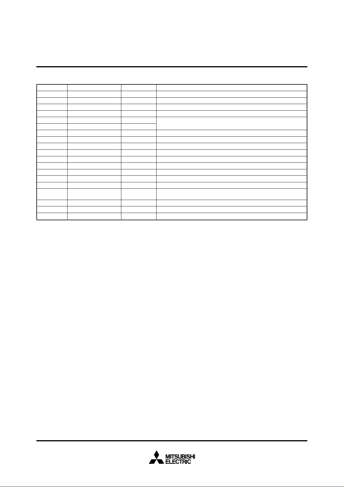
FEATURES
●Number of basic instructions .................................................. 103
●Memory size PROM .............................................124 Kbytes
RAM................................................ 3968 bytes
●Instruction execution time
The fastest instruction at 25 MHz frequency ...................... 160 ns
M37733EHBFS
PROM VERSION OF M37733MHBXXXFP
●Single power supply ...................................................... 5 V ± 1 0%
●Low power dissipation (at 25 MHz frequency)
............................................47.5 mW (Typ.)
●Interrupts ............................................................ 19 types, 7 levels
●Multiple-function 16-bit timer ................................................. 5 + 3
●Serial I/O (UART or clock synchronous) ..................................... 3
●10-bit A-D converter ............................................ 8-channel inputs
●Watchdog timer
●Programmable input/output
(ports P0, P1, P2, P3, P4, P5, P6, P7, P8) ............................... 68
●Clock generating circuit ........................................ 2 circuits built-in
APPLICATION
Control devices for general commercial equipment such as office
automation, office equipment, and so on.
Control devices for general industrial equipment such as
communication equipment, and so on.
Note. Do not use the windowed EPROM version for mass production,
because it is a tool for program development (for evaluation).
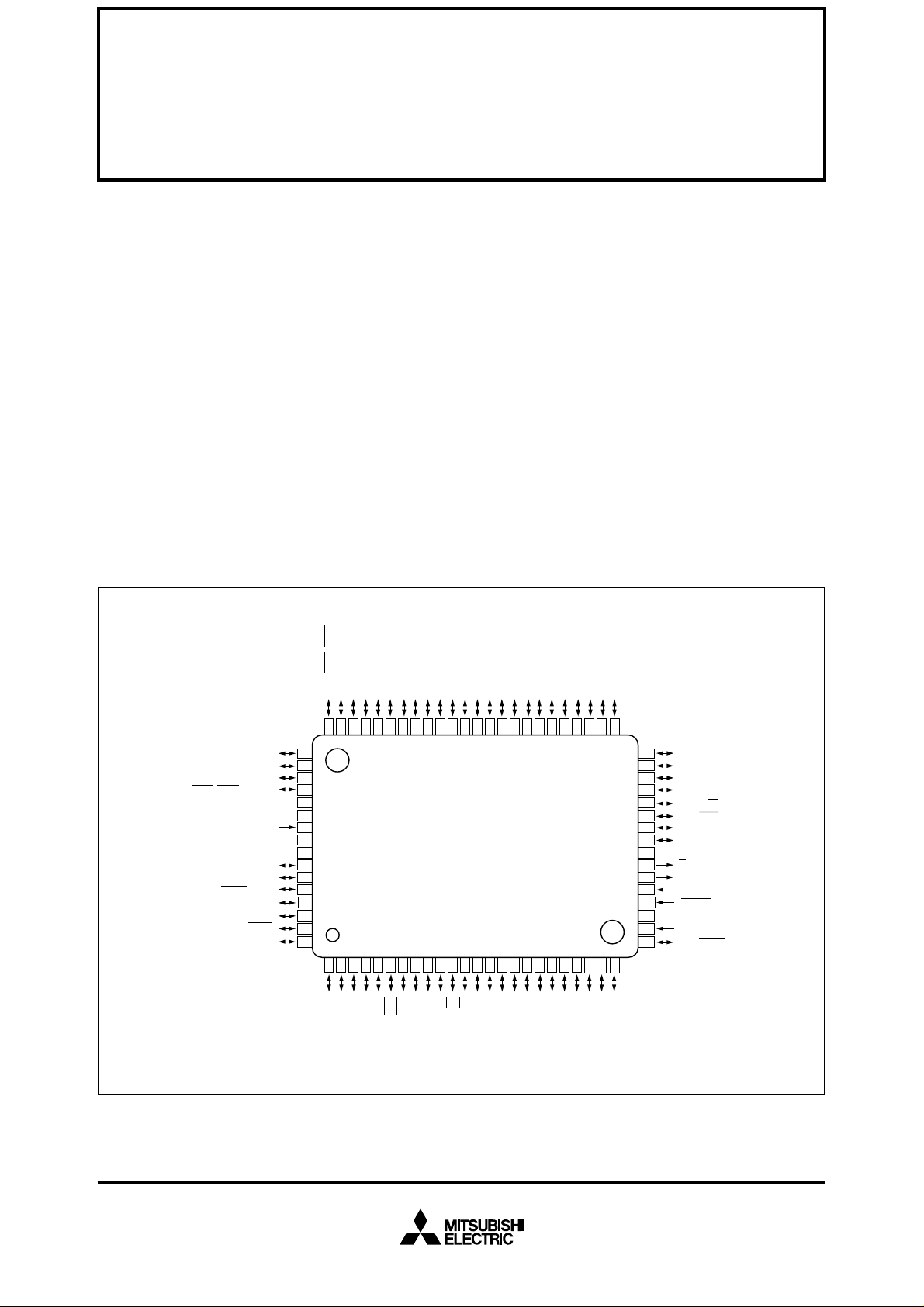
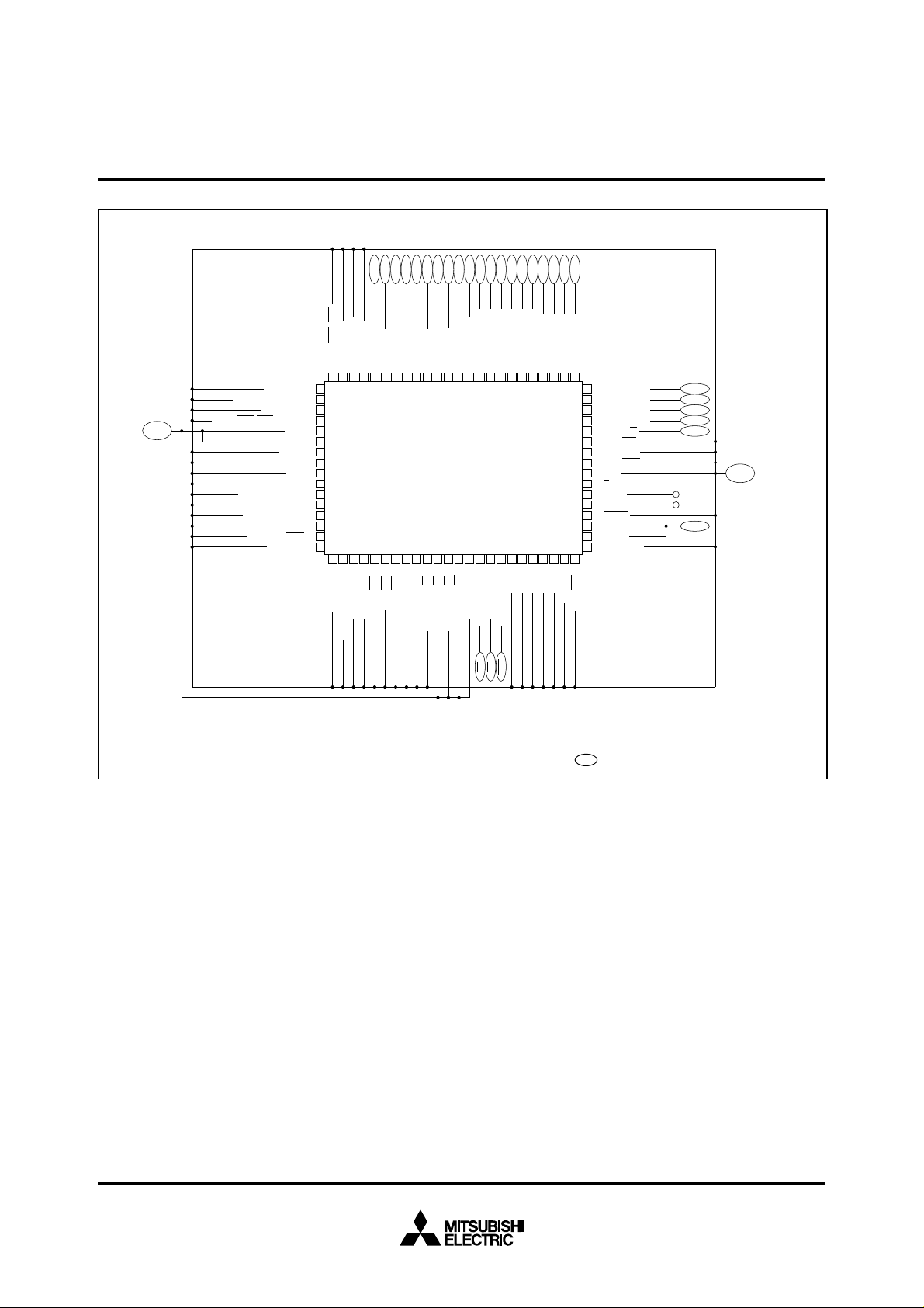
PIN CONFIGURATION (TOP VIEW)
1
RTS
/
1
1
CTS
/
/CLK
4
5
P8
P8
646362
V
REF
V
OUT
65
0
66
0
67
0
6
8
1
69
CC
70
CC
71
72
SS
73
SS
74
IN
75
76
2
77
2
78
2
79
2
80
1
1
2
0
SUB
/AN
/φ
0
IN
P7
/TB2
7
P6
P82/RXD0/CLKS
P8
0
/CTS0/RTS0/
P76/AN6/Xc
P75/AN5/
P83/TXD
P81/CLK
CLKS
AV
V
AV
P77/AN7/Xc
AD
TRG
/TxD
P74/AN4/RxD
P73/AN3/CLK
P72/AN2/CTS
P71/AN
1
D
X
/R
6
P8
3
IN
/TB1
6
P6
1
D
X
/T
7
P8
61
4
IN
/TB0
5
P6
0
1
2
3
4
A
A
/
/
0
1
P0
P0
59
60
5
A
A
A
A
/
/
/
/
2
3
4
5
P0
P0
P0
P0
57
58
56
55
M37733EHBXXXFP
9
8
10
7
6
5
2
1
0
3
IN
KI
OUT
NT
/I
2
P6
/TA4
1
P6
/TA4
0
P6
/
IN
/TA3
7
P5
NT
/I
4
P6
NT
/I
3
P6
6
/A
6
P0
54
11
2
KI
/
OUT
/TA3
6
P5
7
/A
7
P0
53
12
1
KI
/
IN
/TA2
5
P5
8
/D
8
/A
0
P1
52
13
0
KI
/
OUT
/TA2
4
P5
9
/D
9
/A
1
P1
51
14
IN
/TA1
3
P5
10
/D
10
/A
2
P1
50
15
OUT
/TA1
2
P5
11
/D
11
/A
3
P1
49
16
IN
/TA0
1
P5
12
/D
12
/A
4
P1
48
17
OUT
/TA0
0
P5
13
14
15
0
/D
/D
/D
/D
13
14
15
16
/A
/A
/A
/A
5
6
7
0
P1
P1
P1
P2
47
46
44
45
21
18
20
19
P47P46P45P44P4
1
2
3
/D
/D
/D
17
18
19
/A
/A
/A
1
2
3
P2
P2
P2
41
42
43
40
P24/A20/D
39
P25/A21/D
38
P26/A22/D
37
P27/A23/D
36
P30/
35
P31/
34
P32/
33
P33/
32
V
31
E
30
X
29
X
28
RESET
27
CNV
26
BYTE
25
P40/
24
23
22
1
3
/φ
2
RDY
/
1
P4
P4
Outline 80P6N-A
ss
OUT
IN
R/W
BHE
ALE
HLDA
SS
HOLD
4
5
6
7
1
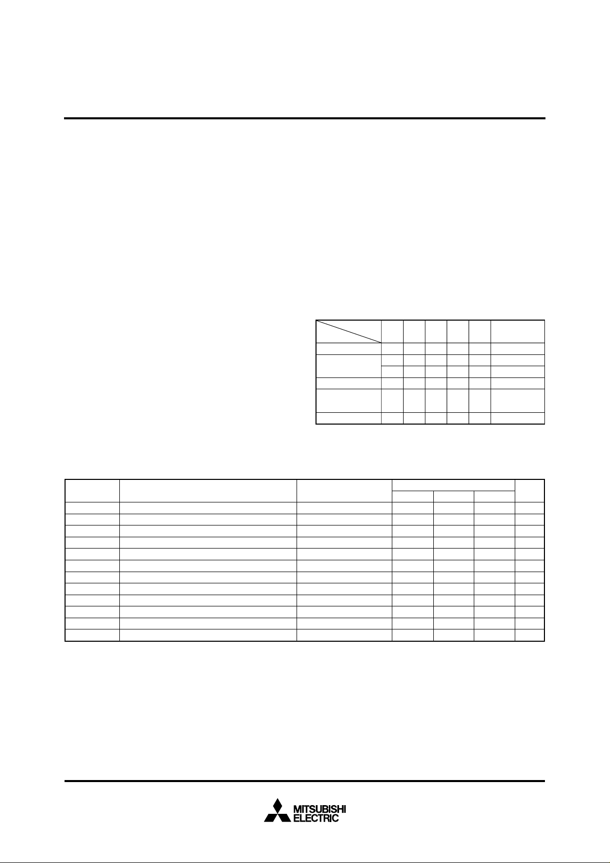
Page 2
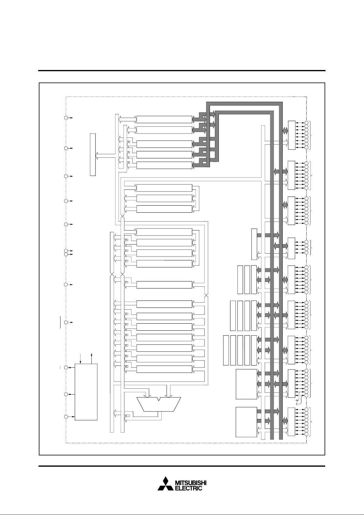
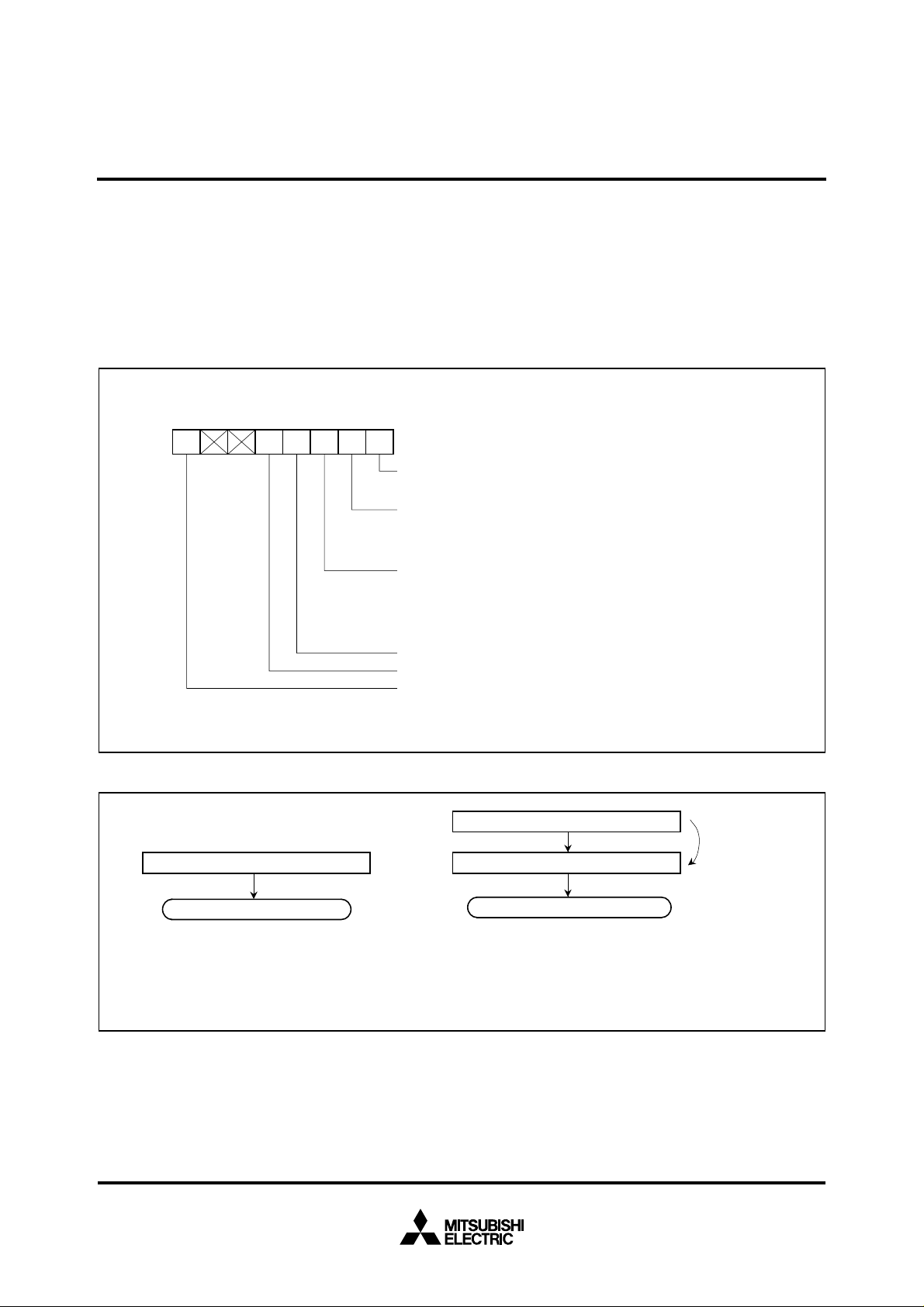
XIN
XOUT
E
RESET
Reset input
VREF
P8(8) P7(8) P5(8)P6(8) P4(8) P3(4)
P2(8) P1(8)
CNVss
BYTE
P0(8)
UART1(9)
UART0(9)
AVSS
(0V)
AVCC
(0V)
V
SS
V
CC
A-D Converter(10)
XCIN
XCOUT
X
CIN
X
COUT
Clock input Clock output
Enable output
Reference
voltage input
External data bus width
selection input
Clock Generating Circuit
Instruction Register(8)
Arithmetic Logic
Unit(16)
Accumulator A(16)
Accumulatcr B(16)
Index Register X(16)
Index Register Y(16)
Stack Pointer S(16)
Direct Page Register DPR(16)
Processor Status Register PS(11)
Input Butter Register IB(16)
Data Bank Register DT(8)
Program Bank Register PG(8)
Program Counter PC(16)
Incrementer/Decrementer(24)
Data Address Register DA(24)
Program Address Register PA(24)
Incrementer(24)
Instruction Queue Buffer Q
2
(8)
Instruction Queue Buffer Q
1
(8)
Instruction Queue Buffer Q
0
(8)
Data Buffer DB
L
(8)
Data Buffer DB
H
(8)
PROM
124 Kbytes
RAM
3968 bytes
Timer TA3(16)
Timer TA4(16)
Timer TA2(16)
Timer TA1(16)
Timer TA0(16)
Watchdog Timer
Timer TB2(16)
Timer TB1(16)
Timer TB0(16)
Address Bus
Data Bus(Odd)
Data Bus(Even)
Input/Output
port P8
Input/Output
port P7
Input/Output
port P6
Input/Output
port P5
Input/Output
port P4
Input/Output
port P3
Input/Output
port P2
Input/Output
port P1
Input/Output
port P0
UART2(9)
MITSUBISHI MICROCOMPUTERS
M37733EHBXXXFP
PRELIMINARY
Notice: This is not a final specification.
Some parametric limits are subject to change.
PROM VERSION OF M37733MHBXXXFP
M37733EHBFS
M37733EHBXXXFP BLOCK DIAGRAM
2
Page 3
MITSUBISHI MICROCOMPUTERS
M37733EHBXXXFP
PRELIMINARY
Notice: This is not a final specification.
Some parametric limits are subject to change.
FUNCTIONS OF M37733EHBXXXFP
Number of basic instructions 103
Instruction execution time 160 ns (the fastest instruction at external clock 25 MHz frequency)
Memory size
Input/Output ports
Multi-function timers
Serial I/O (UART or clock synchronous serial I/O) ✕ 3
A-D converter 10-bit ✕ 1 (8 channels)
Watchdog timer 12-bit ✕ 1
Interrupts
Clock generating circuit
Supply voltage 5 V ± 10%
Power dissipation 47.5 mW (at external clock 25 MHz frequency)
Input/Output characteristic
Memory expansion Maximum 16 Mbytes
Operating temperature range –20 to 85 °C
Device structure CMOS high-performance silicon gate process
Package
Parameter Functions
PROM 124 Kbytes
RAM 3968 bytes
P0 – P2, P4 – P8 8-bit ✕ 8
P3 4-bit ✕ 1
TA0, TA1, TA2, TA3, TA4 16-bit ✕ 5
TB0, TB1, TB2 16-bit ✕ 3
3 external types, 16 internal types
Each interrupt can be set to the priority level (0 – 7.)
2 circuits built-in (externally connected to a ceramic resonator or a
quartz-crystal oscillator)
Input/Output voltage 5 V
Output current 5 mA
M37733EHBXXXFP 80-pin plastic molded QFP (80P6N-A)
M37733EHBFS 80-pin ceramic LCC (with a window) (80D0)
PROM VERSION OF M37733MHBXXXFP
M37733EHBFS
3
Page 4
MITSUBISHI MICROCOMPUTERS
M37733EHBXXXFP
PRELIMINARY
Notice: This is not a final specification.
Some parametric limits are subject to change.
PIN DESCRIPTION
Pin Name Input/Output Functions
Vcc, Power source Apply 5 V ± 10% to Vcc and 0 V to Vss.
Vss
CNVss CNVss input Input This pin controls the processor mode. Connect to Vss for the single-chip mode and the memory
_____
RESET Reset input Input When “L” level is applied to this pin, the microcomputer enters the reset state.
XIN Clock input Input
XOUT Clock output Output
_
E Enable output Output This pin functions as the enable signal output pin which indicates the access status in the internal
BYTE
External data
Input In the memory expansion mode or the microprocessor mode, this pin determines whether the
bus width
selection input
AVcc, Analog power Power source input pin for the A-D converter. Externally connect AVcc to Vcc and AVss to Vss.
AVss source input
REF Reference Input This is reference voltage input pin for the A-D converter.
V
voltage input
0 – P07 I/O port P0 I/O In the single-chip mode, port P0 becomes an 8-bit I/O port. An I/O direction register is available so
P0
0 – P17 I/O port P1 I/O In the single-chip mode, these pins have the same functions as port P0. When the BYTE pin is set
P1
0 – P27 I/O port P2 I/O In the single-chip mode, these pins have the same functions as port P0. In the memory expansion
P2
0 – P33 I/O port P3 I/O In the single-chip mode, these pins have the same function as port P0. In the memory expansion
P3
0 – P47 I/O port P4 I/O In the single-chip mode, these pins have the same functions as port P0. In the memory expansion
P4
0 – P57 I/O port P5 I/O In addition to having the same functions as port P0 in the single-chip mode, these pins also
P5
0 – P67 I/O port P6 I/O In addition to having the same functions as port P0 in the single-chip mode, these pins also
P6
0 – P77 I/O port P7 I/O In addition to having the same functions as port P0 in the single-chip mode, these pins function as
P7
0 – P87 I/O port P8 I/O In addition to having the same functions as port P0 in the single-chip mode, these pins also
P8
expansion mode, and to Vcc for the microprocessor mode.
These are pins of main-clock generating circuit. Connect a ceramic resonator or a quartzcrystal oscillator between X
IN and XOUT. When an external clock is used, the clock source should
be connected to the XIN pin, and the XOUT pin should be left open.
bus. When output level of E signal is “L”, data/instruction read or data write is performed.
_
external data bus has an 8-bit width or a 16-bit width. The data bus has a 16-bit width when “L”
signal is input and an 8-bit width when “H” signal is input.
that each pin can be programmed for input or output. These ports are in the input mode when
reset.
In the memory expansion mode or the microprocessor mode, these pins output address (A0 – A7).
to “L” in the memory expansion mode or the microprocessor mode and external data bus has a
16-bit width, high-order data (D8 – D15) is input/output or an address (A8 – A15) is output. When
the BYTE pin is “H” and an external data bus has an 8-bit width, only address (A8 – A15) is output.
mode or the microprocessor mode, low-order data (D
(A0 – A7) is output .
mode or the microprocessor mode, R/W, BHE, ALE, and HLDA signals are output.
__ ____ _____
mode or the microprocessor mode, P40, P41, and P42 become HOLD and RDY input pins, and a
clock
φ1 output pin, respectively. Functions of the other pins are the same as in the single-chip
mode. However, in the memory expansion mode, P42 can be selected as an I/O port.
function as I/O pins for timers A0 to A3 and input pins for key input interrupt input (KI0 – KI3 ).
function as I/O pins for timer A4, input pins for external interrupt input (INT0 – INT2) and input pins
for timers B0 to B2. P67 also functions as sub-clock φSUB output pin.
input pins for A-D converter. P7
7 have the function as the output pin (XCOUT) and the input pin (XCIN) of the sub-clock (32 kHz)
P7
oscillation circuit, respectively. When P7
2 to P75 also function as I/O pins for UART2. Additionally, P76 and
6 and P77 are used as the XCOUT and XCIN pins, connect
a resonator or an oscillator between the both.
function as I/O pins for UART 0 and UART 1.
PROM VERSION OF M37733MHBXXXFP
0 – D7) is input/output or an address
M37733EHBFS
_____ ____
__ __
____ ____
4
Page 5
MITSUBISHI MICROCOMPUTERS
M37733EHBXXXFP
PRELIMINARY
Notice: This is not a final specification.
Some parametric limits are subject to change.
PIN DESCRIPTION (EPROM MODE)
Pin
VCC, VSS
CNVSS
BYTE
_____
RESET
XIN
XOUT
_
E
AVCC, AVSS
VREF
P00 – P07
P10 – P17
P20 – P27
P30
P31 – P33
P40 – P47
P50 – P57
P60 – P67
P70 – P77
P80 – P87
Power supply
VPP input
VPP input
Reset input
Clock input
Clock output
Enable output
Analog supply input
Reference voltage input
Address input (A0 – A7)
Address input (A8 – A15)
Data I/O (D0 – D7)
Address input (A16)
Input port P3
Input port P4
Control signal input
Input port P6
Input port P7
Input port P8
Name
Input/Output
Input
Input
Input
Input
Output
Output
Input
Input
Input
I/O
Input
Input
Input
Input
Input
Input
Input
PROM VERSION OF M37733MHBXXXFP
Functions
Supply 5V±10% to VCC and 0V to VSS.
Connect to VPP when programming or verifing.
Connect to VPP when programming or verifing.
Connect to VSS.
Connect a ceramic resonator between XIN and XOUT.
Keep open.
Connect AVCC to VCC and AVSS to VSS.
Connect to VSS.
Port P0 functions as the lower 8 bits address input (A0 – A7).
Port P1 functions as the higher 8 bits address input (A8 – A15).
Port P2 functions as the 8 bits data input/output (D0 – D7).
P30 functions as the most significant bit address input (A16).
Connect to VSS.
Connect to VSS.
P50, P51, and P52 function as PGM, OE, and CE input pins respectively.
Connect P5
Connect to VSS.
Connect to VSS.
Connect to VSS.
3, P54, P55, and P56 to VCC. Connect P57 to VSS.
_____ ___ ___
M37733EHBFS
5
Page 6
MITSUBISHI MICROCOMPUTERS
M37733EHBXXXFP
PRELIMINARY
Notice: This is not a final specification.
Some parametric limits are subject to change.
PROM VERSION OF M37733MHBXXXFP
M37733EHBFS
BASIC FUNCTION BLOCKS
The M37733EHBXXXFP has the same functions as the
M37733MHBXXXFP except for the following:
(1) The built-in ROM is PROM.
(2) The status of bit 3 of the oscillation circuit control register 1 (address
6F
16) at a reset is different.
(3) The usage condition of bit 3 of the oscillation circuit control register
1 is different.
76543210
1
0
CC
CC
2
Oscillation circuit control register 1
CC
0
1
Main clock division selection bit
0 : Main clock is divided by 2.
1 : Main clock is not divided by 2.
Main clock external input selection bit
0 : Main-clock oscillation circuit is operating by itself.
Watchdog timer is used at returning from STP state.
1 : Main-clock is input externally.
Watchdog timer is not used at returning from STP state.
Sub clock external input selection bit
0 : Sub-clock oscillation circuit is operating by itself.
Port P7
Watchdog timer is used at returning from STP state.
1 : Sub-clock is input externally.
Port P7
Watchdog timer is not used at returning from STP state.
1 : Always “1” (“1” at reset)
0 : Always “0” (However, writing data “55
Clock prescaler reset bit
Accordingly, refer to the basic function blocks description in the
M37733MHBXXXFP except for Figure 1 (bit configuration of the
oscillation circuit control register 1) and Figure 3 (microcomputer
internal status during reset).
In the M37733EHBXXXFP, bit 3 of the oscillation circuit control
register 1 must be “1”. (Refer to Figure 1.) The status of this bit at
a reset is “1”.
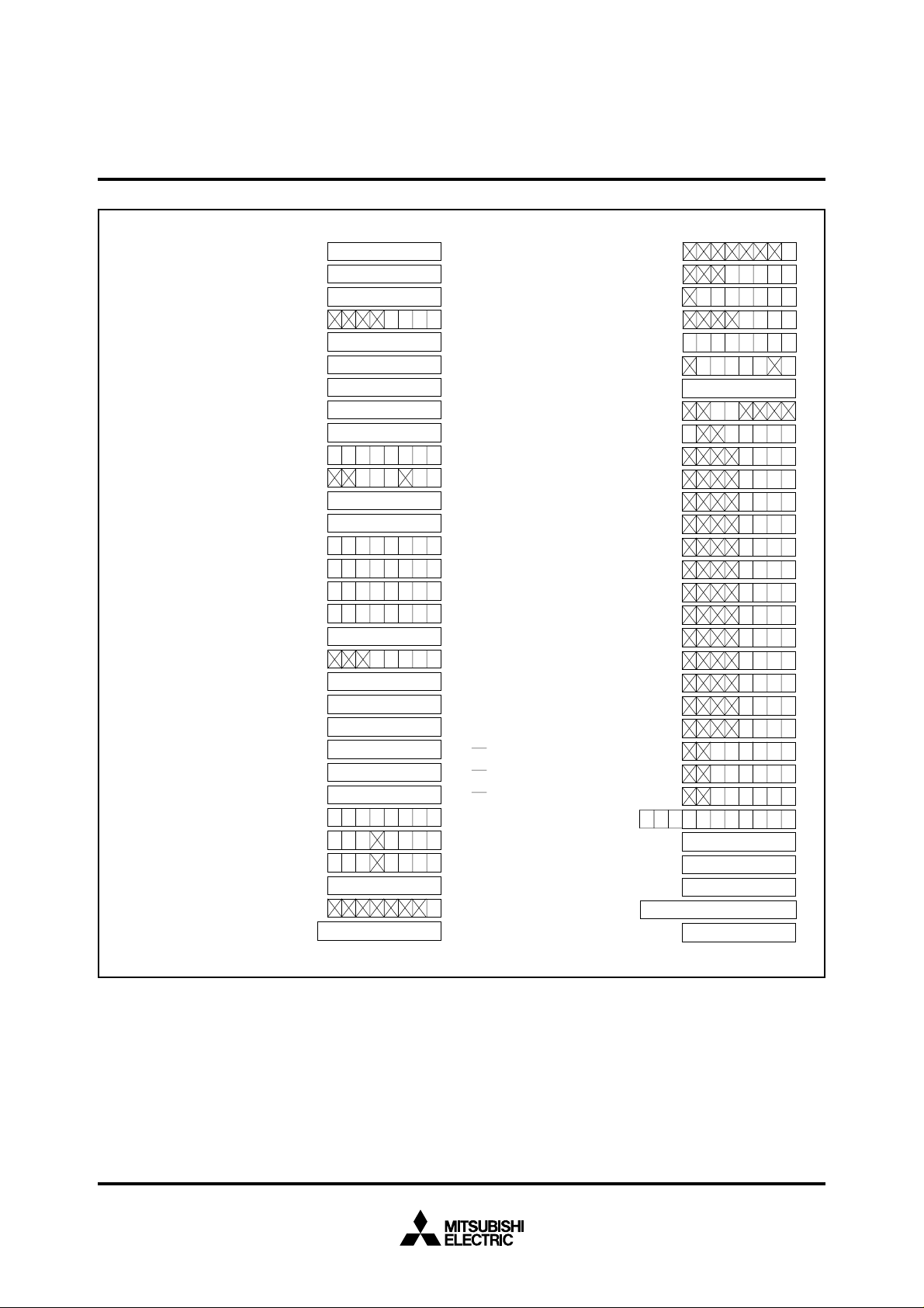
Address
16
6F
Note. Write to the oscillation circuit control
register 1 as the flow shown in Figure 2.
6
functions as X
6
functions as I/O port.
COUT
pin.
16
” shown in Figure 2 is possible.)
Fig. 1 Bit configuration of oscillation circuit control register 1 (corresponding to Figure 63 in data sheet “M37733MHBXXXFP”)
Writing data “55
16
” (LDM instruction)
Next instruction
16
Writing data “8016” (LDM instruction)
Reset clock prescaler
Writing data “0Y
CC
• How to reset clock prescaler • How to write in CC
” (LDM instruction)
2
to CC0 selection bits
2
to CC0 selection bits
Note. “Y” is the sum of bits to be set. For example, when
setting bits 2 and 1 to “1”, “Y” becomes “6”.
Fig. 2 How to write data in oscillation circuit control register 1 (identical with Figure 64 in data sheet “M37733MHBXXXFP”)
6
Page 7
MITSUBISHI MICROCOMPUTERS
M37733EHBXXXFP
PRELIMINARY
Notice: This is not a final specification.
Some parametric limits are subject to change.
PROM VERSION OF M37733MHBXXXFP
M37733EHBFS
Address
Port P0 direction register
Port P1 direction register
Port P2 direction register
Port P3 direction register
Port P4 direction register
Port P5 direction register
Port P6 direction register
Port P7 direction register
Port P8 direction register
A-D control register 0
A-D control register 1
UART 0 transmit/receive mode register
UART 1 transmit/receive mode register
UART 0 transmit/receive
control register 0
UART 1 transmit/receive
control register 0
UART 0 transmit/receive
control register 1
UART 1 transmit/receive
control register 1
Count start flag
One- shot start flag
Up-down flag
Timer A0 mode register
Timer A1 mode register
Timer A2 mode register
Timer A3 mode register
Timer A4 mode register
Timer B0 mode register
Timer B1 mode register
Timer B2 mode register
Processor mode register 0
Processor mode register 1
Watchdog timer register
(0416)
(0516)
(0816)
(0916)
(0C16)
(0D16)
(1016)
(1116)
(1416)
(1E16)
(1F16)
(3016)
(3816)
(3416)
(3C16)
(3516)
(3D16)
(4016)
(4216)
(4416)
(5616)
(5716)
(5816)
(5916)
(5A16)
(5B16)
(5C16)
(5D16)
(5E16)
(5F16)
(6016)
•••
•••
•••
•••
•••
•••
•••
•••
•••
0000
•••
0
•••
•••
•••
•••
0000
•••
0000
•••
0000
•••
•••
•••
•••
•••
•••
•••
•••
•••
•••
001
•••
001 00 00
•••
•••
•••
•••
00
16
00
16
00
16
0000
00
16
00
16
00
16
00
16
00
16
0
00
16
00
00
16
1000
000010
16
00
000 00
00
16
00
16
00
16
00
16
00
16
00
16
0001 00 00
00 00
00
16
FFF
16
???
11
0000
0010
10
0
Address
Watchdog timer frequency selection flag
Memory allocation control register
UART2 transmit/receive mode register
UART2 transmit/receive control register 0
UART2 transmit/receive control register 1
Oscillation circuit control register 0
Port function control register
Serial transmit control register
Oscillation circuit control register 1
A-D/UART2 trans./rece. interrupt control register
UART 0 transmission interrupt control register
UART 0 receive interrupt control register
UART 1 transmission interrupt control register
UART 1 receive interrupt control register
Timer A0 interrupt control register
Timer A1 interrupt control register
Timer A2 interrupt control register
Timer A3 interrupt control register
Timer A4 interrupt control register
Timer B0 interrupt control register
Timer B1 interrupt control register
Timer B2 interrupt control register
INT
0
interrupt control register
INT
1
interrupt control register
INT
2
/Key input interrupt control register
Processor status register (PS)
Program bank register (PG)
H
Program counter (PC
Program counter (PC
Direct page register (DPR)
Data bank register (DT)
)
L
)
(6116)
(6316)
(6416)
(6816)
(69
(6C16)
(6D16)
(6E16)
(6F16)
(7016)
(7116)
(7216)
(7316)
(7416)
(7516)
(7616)
(7716)
(7816)
(7916)
(7A16)
(7B16)
(7C16)
(7D16)
(7E16)
(7F16)
16)•••
•••
0 0
•••
0 000000
•••
•••
0 0100000
0
00
0 01000
0
•••
0
•••
00
00
•••
0
•••
•••
•••
•••
•••
•••
•••
•••
•••
•••
•••
•••
•••
•••
0
•••
0
•••
0
•••
?000
?
Content of FFFF
Content of FFFE
0000
000
00
1
0
00
16
1
0
0000
0000
0000
0000
0000
0000
0000
0000
0000
0000
0000
0000
0000
0
0
0
0
0
0
0
00
16
00
16
00
16
0
0
0
001
00
000
001
000
000
000
000
1??
16
16
Fig. 3 Microcomputer internal status during reset
Contents of other registers and RAM are undefined during reset. Initialize them by software.
7
Page 8
MITSUBISHI MICROCOMPUTERS
M37733EHBXXXFP
PRELIMINARY
Notice: This is not a final specification.
Some parametric limits are subject to change.
PROM VERSION OF M37733MHBXXXFP
M37733EHBFS
EPROM MODE
The M37733EHBXXXFP features an EPROM mode in addition to its
normal modes. When the RESET signal level is “L”, the chip
automatically enters the EPROM mode. Table 1 list the
correspondence between pins and Figure 4 shows the pin
connections in the EPROM mode.
The EPROM mode is the 1M mode for the EPROM that is equivalent
to the M5M27C101K.
When in the EPROM mode, ports P0, P1, P2, P3
CNV
SS, and BYTE are used for the EPROM (equivalent to the
Table 1 Pin function in EPROM mode
M37733EHBXXXFP
VCC
VPP
VSS
Address input
Data I/O
___
CE
___
OE
_____
PGM
_____
VCC
CNVSS, BYTE
VSS
Ports P0, P1, P30
Port P2
P52
P51
P50
0, P50, P51, P52,
M5M27C101K
VCC
VPP
VSS
A0 – A16
D0 – D7
___
CE
___
OE
_____
PGM
M5M27C101K).
When in this mode, the built-in PROM can be programmed or read
from using these pins in the same way as with the M5M27C101K.
This chip does not have Device Identifier Mode, so that set the
corresponding program algorithm. The program area should specify
address 01000
16 – 1FFFF16.
Connect the clock which is either ceramic resonator or external clock
to X
IN pin and XOUT pin.
8
Page 9
MITSUBISHI MICROCOMPUTERS
M37733EHBXXXFP
PRELIMINARY
Notice: This is not a final specification.
Some parametric limits are subject to change.
PROM VERSION OF M37733MHBXXXFP
A6
A7
A0
A1
A2
A3
A8
A4
A9
A5
A10
A11
D0
D1
D2
A13
A14
A12
D3
A15
M37733EHBFS
P81/CLK0
VCC
P80/CTS0/RTS 0/CLKS1
VCC
AVCC
VREF
AVSS
VSS
Fig. 4 Pin connection in EPROM mode
P04/A4
P84/CTS1/RTS 1
P86/RXD1
P87/TXD1
P00/A0
P85/CLK1
↔
↔
↔
↔
↔
62
61
63
64
65
↔ P83/TXD0
66
↔ P82/RXD0/CLKS0
67
↔
68
↔
69
70
71
→
72
73
74
↔ P77/AN7/XCIN
75
↔ P76/AN6/XCOUT
76
↔ P75/AN5/ADTRG /TXD2
77
↔ P74/AN4/RXD2
78
↔ P73/AN3/CLK2
79
↔ P72/AN2/CTS2
80
↔ P71/AN1
60
3
4
5
1
2
↔
↔
↔
↔
↔
P64/INT2
P70/AN0
P66/TB1IN
P65/TB0IN
P67/TB2IN/φSUB
P05/A5
P06/A6
P03/A3
P01/A1
P02/A2
↔
↔
↔
↔
↔
↔
58
57
56
59
54
55
M37733EHBXXXFP
7
8
9
6
10
11
↔
↔
P63/INT1
↔
↔
↔
↔
P62/INT0
P61/TA4IN
P60/TA4OUT
P57/TA3IN/KI3
P56/TA3OUT/KI2
P13/A11/D11
P10/A8/D8
P11/A9/D9
P07/A7
P12/A10/D10
↔
↔
↔
↔
↔
53
52
49
51
50
12
13
14
15
16
↔
↔
↔
↔
↔
P51/TA0IN
P53/TA1IN
P52/TA1OUT
P55/TA2IN/KI1
P54/TA2OUT/KI0
CE
OE
48
17
P14/A12/D12
↔
↔
P50/TA0OUT
PGM
P20/A16/D0
P21/A17/D1
P15/A13/D13
↔
47
18
↔
P47
P22/A18/D2
P16/A14/D14
↔
46
19
↔
P46
P23/A19/D3
P17/A15/D15
↔
↔
↔
↔
↔
45
44
41
42
43
40
↔P24/A20/D4
39
↔P25/A21/D5
38
↔P26/A22/D6
37
↔P27/A23/D7
36
↔P30/R/W
35
↔P31/BHE
34
↔P32/ALE
33
↔P33/HLDA
32
VSS
31
→ E
30
→ XOUT
29
← XIN
28
← RESET
27
CNVSS
26
← BYTE
25
21
20
↔
↔
P45
P44
↔P40/HOLD
22
23
24
↔
↔
↔
φ1
P43
P42/
P41/RDY
D4
D5
D6
D7
A16
VSS
∗
VPP
✽ : Connect to ceramic oscillation circuit.
Outline 80P6N-A
: It is used in the EPROM mode.
9
Page 10
MITSUBISHI MICROCOMPUTERS
M37733EHBXXXFP
PRELIMINARY
Notice: This is not a final specification.
Some parametric limits are subject to change.
PROM VERSION OF M37733MHBXXXFP
M37733EHBFS
FUNCTION IN EPROM MODE
1M mode (equivalent to the M5M27C101K)
Reading
To read the EPROM, set the CE and OE pins to a “L” level. Input the
address of the data (A
to the I/O pins D
__ __
the CE or OE pins are in the “H” state.
0 – D7. The data I/O pins will be floating when either
___ ___
0 – A16) to be read, and the data will be output
Programming
Programming must be performed in 8 bits by a byte program. To
program to the EPROM, set the CE pin to a “L” level and the OE pin to
a “H” level. The CPU will enter the programming mode when 12.5 V
is applied to the V
with pins A
– D7. Set the PGM pin to a “L” level to being programming.
PP pin. The address to be programmed to is selected
0 – A16, and the data to be programmed is input to pins D0
_____
___ ___
Erasing
To erase data on this chip, use an ultraviolet light source with a 2537
Angstrom wave length. The minimum radiation power necessary for
erasing is 15 J/cm
2
.
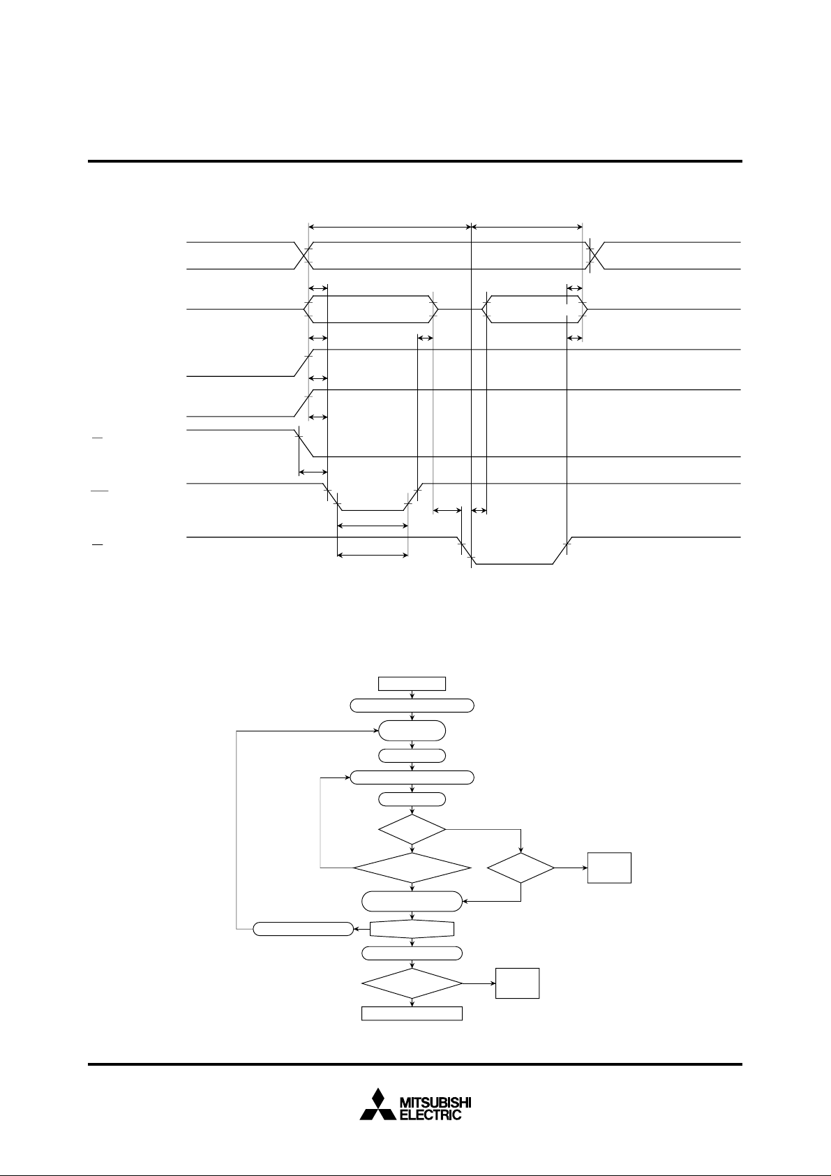
Programming operation
To program the M37733EHBXXXFP, first set VCC = 6 V, VPP = 12.5
V, and set the address to 01000
pulse, check that the data can be read, and if it cannot be read OK,
repeat the procedure, applying a 0.2 ms programming pulse and
checking that the data can be read until it can be read OK. Record
the accumulated number of pulse applied (X) before the data can be
read OK, and then write the data again, applying a further once this
number of pulses (0.2 ✕ X ms).
When this series of programming operations is complete, increment
the address, and continue to repeat the procedure above until the
last address has been reached.
Finally, when all addresses have been programmed, read with V
V
PP = 5 V (or VCC = VPP = 5.5 V).
Table 2. I/O signal in each mode
___CE___OE_____
Pin
Mode
Read-out
Output
Disable
Programming
Programming
Verify
Program Disable
VIL
VIL
VIH
VIL
VIL
VIH
Note 1 : An X indicates either V
16. Apply a 0.2 ms programming
PGM VPP VCC Data I/O
VIL
X
5 V
5 V
VIH
X
5 V
5 V
X
X
5 V
5 V
VIH
VIL
12.5 V
6 V
VIL
VIH
12.5 V
6 V
VIH
VIH
12.5 V
6 V
IL or VIH.
CC =
Output
Floating
Floating
Input
Output
Floating
Programming operation (equivalent to the M5M27C101K)
AC ELECTRICAL CHARACTERISTICS (Ta = 25 ± 5 °C, VCC = 6 V ± 0.25 V, VPP = 12.5 ± 0.3 V, unless otherwise noted)
Symbol Parameter Test conditions
tAS
tOES
tDS
tAH
tDH
tDFP
tVCS
tVPS
tPW
tOPW
tCES
tOE
Address setup time
___
OE setup time
Data setup time
Address hold time
Data hold time
Output enable to output float delay
VCC setup time
VPP setup time
_____
PGM pulse width
_____
PGM over program pulse width
___
CE setup time
Data valid from OE
__
Min.
0.19
0.19
Limits
Typ.
2
2
2
0
2
0
2
2
0.2
2
Max.
130
0.21
5.25
150
Unit
µs
µs
µs
µs
µs
ns
µs
µs
ms
ms
µs
ns
10
Page 11
MITSUBISHI MICROCOMPUTERS
M37733EHBXXXFP
PRELIMINARY
Notice: This is not a final specification.
Some parametric limits are subject to change.
AC waveforms
V
VIH/VOH
VIL/VOL
VPP
VCC
VCC +1
V
VIH
VIH
VIH
IH
VIL
CC
VIL
VIL
VIL
ADDRESS
DATA
PP
V
VCC
CE
PGM
OE
tAS
tVPS
tVCS
tCES
PROGRAM VERIFY
DATA SET
DATA OUTPUT VALID
tDH tDS
tOES tOE
tPW
tOPW
PROM VERSION OF M37733MHBXXXFP
M37733EHBFS
tAH
tDFP
Programming algorithm flow chart
INCREMENT ADDR
START
ADDR=FIRST LOCATION
V
CC
PP
=12.5 V
V
X=0
PROGRAM ONE PULSE OF 0.2 ms
X=X+1
X=25?
NO
FAIL
VERIFY
BYTE
PROGRAM PULSE OF
0.2X ms DURATION
NO
LAST ADDR?
V
CC=VPP
VERIFY
ALL BYTE
DEVICE PASSED
Test conditions for A.C. characteristics
Input voltage : V
IL = 0.45 V, VIH = 2.4 V
Input rise and fall times (10 % – 90 %) : ≤ 20 ns
Reference voltage at timing measurement : Input, Output
“L” = 0.8 V, “H” = 2 V
=6.0 V
YES
PASS
=*5.0 V
PASS
YES
FAIL
VERIFY
BYTE
DEVICE
FAILED
PASS
FAIL
DEVICE
FAILED
*4.5 V ≤ VCC = VPP ≤ 5.5 V
11
Page 12

PRELIMINARY
Notice: This is not a final specification.
Some parametric limits are subject to change.
SAFETY INSTRUCTIONS
(1)Sunlight and fluorescent lamp contain light that can erase written
information. When using in read mode, be sure to cover the
transparent glass portion with a seal or other materials (ceramic
package product).
(2)Mitsubishi Electric corp. provides the seal for covering the
transparent glass. Take care that the seal does not touch the read
pins (ceramic package product).
(3)Clean the transparent glass before erasing. Fingers’ fat and paste
disturb the passage of ultraviolet rays and may affect badly the
erasure capability (ceramic package product).
(4) A high voltage is used for programming. Take care that over-
voltage is not applied. Take care especially at power on.
(5)The programmable M37733EHBFP that is shipped in blank is also
provided. For the M37733EHBFP, Mitsubishi Electric corp. does
not perform PROM programming test and screening following the
assembly processes. To improve reliability after programming,
performing programming and test according to the flow below
before use is recommended.
MITSUBISHI MICROCOMPUTERS
M37733EHBXXXFP
M37733EHBFS
PROM VERSION OF M37733MHBXXXFP
ADDRESSING MODES
The M37733EHBXXXFP has 28 powerful addressing modes. Refer
to the “7700 Family Software Manual” for the details.
MACHINE INSTRUCTION LIST
The M37733EHBXXXFP has 103 machine instructions. Refer to the
“7700 Family Software Manual” for the details.
DATA REQUIRED FOR PROM ORDERING
Please send the following data for writing to PROM.
(1)M37733EHBXXXFP writing to PROM order confirmation form
(2)80P6N mark specification form
(3)ROM data (EPROM 3 sets)
Programming with PROM programmer
Screening
(Leave at 150 °C for 40 hours)
Verify test with PROM programmer
Function check in target device
Caution : Never expose to 150 °C exceeding 100 hours.
(Caution)
12
Page 13

MITSUBISHI MICROCOMPUTERS
M37733EHBXXXFP
PRELIMINARY
Notice: This is not a final specification.
Some parametric limits are subject to change.
ABSOLUTE MAXIMUM RATINGS
Symbol Parameter Conditions Ratings Unit
Vcc Power source voltage –0.3 to +7 V
AVcc Analog power source voltage –0.3 to +7 V
VI
Input voltage RESET, CNVss, BYTE –0.3 to +12 (Note) V
Input voltage P0
V
I
Output voltage
VO
Pd Power dissipation Ta = 25 °C 300 mW
Topr Operating temperature –20 to +85 °C
stg Storage temperature –40 to +150 °C
T
Note. When the EPROM is programmed, input voltage of pins CNVss and BYTE is 13 V respectively.
_____
0 – P07, P10 – P17, P20 – P27,
0 – P33, P40 – P47, P50 – P57,
P3
0 – P67, P70 – P77, P80 – P87,
P6
VREF, XIN
P00 – P07, P10 – P17, P20 – P27,
0 – P33, P40 – P47, P50 – P57,
P3
0 – P67, P70 – P77, P80 – P87,
P6
_
XOUT, E
PROM VERSION OF M37733MHBXXXFP
M37733EHBFS
–0.3 to Vcc + 0.3 V
–0.3 to Vcc + 0.3 V
RECOMMENDED OPERATING CONDITIONS (Vcc = 5 V ± 10%, Ta = –20 to +85 °C, unless otherwise noted)
Symbol Parameter
IN) : Operating 4.5 5.0 5.5
Vcc Power source voltage
f(X
f(XIN) : Stopped, f(XCIN) = 32.768 kHz 2.7 5.5
Min. Typ. Max.
AVcc Analog power source voltage Vcc V
Vss Power source voltage 0V
AVss Analog power source voltage 0 V
IH
V
VIH
VIH
VIL
VIL
VIL
IOH(peak)
High-level input voltage P0
P70 – P77, P80 – P87, XIN, RESET, CNVss, BYTE, XCIN (Note 3)
High-level input voltage P10 – P17, P20 – P27 (in single-chip mode)
High-level input voltage P1
(in memory expansion mode and microprocessor mode)
Low-level input voltage P0
P70 – P77, P80 – P87, XIN, RESET, CNVss, BYTE, XCIN (Note 3)
Low-level input voltage P10 – P17, P20 – P27 (in single-chip mode)
Low-level input voltage P1
(in memory expansion mode and microprocessor mode)
High-level peak output current P0
0 – P07, P30 – P33, P40 – P47, P50 – P57, P60 – P67,
0 – P17, P20 – P27
0 – P07, P30 – P33, P40 – P47, P50 – P57, P60 – P67,
0 – P17, P20 – P27
0 – P07, P10 – P17, P20 – P27, P30 – P33,
0 – P47, P50 – P57, P60 – P67, P70 – P77,
P4
_______
_______
0.8 Vcc
0.8 Vcc
0.5 Vcc
0
0
0
P80 – P87
High-level average output current P00 – P07, P10 – P17, P20 – P27, P30 – P33,
IOH(avg)
P4
0 – P47, P50 – P57, P60 – P67, P70 – P77,
P80 – P87
Low-level peak output current P00 – P07, P10 – P17, P20 – P27, P30 – P33,
IOL(peak)
0 – P43, P54 – P57, P60 – P67, P70 – P77,
P4
P80 – P87
IOL(peak)
Low-level peak output current P44 – P47, P50 – P53
Low-level average output current P00 – P07, P10 – P17, P20 – P27, P30 – P33,
0 – P43, P54 – P57, P60 – P67, P70 – P77,
IOL(avg)
P4
P80 – P87
IOL(avg) Low-level average output current P44 – P47, P50 – P53 15 mA
f(XIN) Main-clock oscillation frequency (Note 4) 25 MHz
CIN) Sub-clock oscillation frequency 32.768 50 kHz
f(X
Notes 1. Average output current is the average value of a 100 ms interval.
2. The sum of I
the sum of I
the sum of I
the sum of I
3. Limits V
4. The maximum value of f(X
OL(peak) for ports P0, P1, P2, P3, and P8 must be 80 mA or less,
OH(peak) for ports P0, P1, P2, P3, and P8 must be 80 mA or less,
OL(peak) for ports P4, P5, P6, and P7 must be 100 mA or less, and
OH(peak) for ports P4, P5, P6, and P7 must be 80 mA or less.
IH and VIL for XCIN are applied when the sub clock external input selection bit = “1”.
IN) = 12.5 MHz when the main clock division selection bit = “1”.
Limits
Vcc
Vcc
Vcc
0.2Vcc
0.2Vcc
0.16Vcc
–10
–5
10
20
5
Unit
V
V
V
V
V
V
V
mA
mA
mA
mA
mA
13
Page 14

MITSUBISHI MICROCOMPUTERS
M37733EHBXXXFP
PRELIMINARY
Notice: This is not a final specification.
Some parametric limits are subject to change.
ELECTRICAL CHARACTERISTICS (Vcc = 5 V, Vss = 0 V, Ta = –20 to 85 °C, f(XIN) = 25 MHz, unless otherwise noted)
Symbol Parameter Test conditions
OH P33, P40 – P47, P50 – P57,IOH = –10 mA 3 V
V
V
OH
High-level output voltage P00 – P07, P10 – P17, P20 – P27,
VOH High-level output voltage P30 – P32
High-level output voltage P0
OH High-level output voltage
V
Low-level output voltage P0
OL P33, P40 – P43, P54 – P57,IOL = 10 mA 2 V
V
VOL Low-level output voltage P44 – P47, P50 – P53 IOL = 20 mA 2 V
VOL
Low-level output voltage P0
VOL Low-level output voltage P30 – P32
OL
V
T+ – VT–
V
VT+ – VT–
Low-level output voltage E
Hysteresis
Hysteresis RESET 0.2 0.5 V
______ ____
HOLD, RDY, TA0IN – TA4IN, TB0IN – TB2IN,
___ ___ ____ ___ ___ ___
INT0 – INT2, ADTRG, CTS0, CTS1, CTS2, CLK0, 0.4 1 V
CLK1, CLK2, KI0 – KI3
_____
VT+ – VT– Hysteresis XIN 0.1 0.4 V
VT+ – VT– Hysteresis XCIN (When external clock is input) 0.1 0.4 V
High-level input current
0 – P07, P10 – P17, P20 – P27, P30 – P33,
IIH
P0
0 – P47, P50 – P57, P60 – P67, P70 – P77,
P4
P80 – P87, XIN, RESET, CNVss, BYTE
Low-level input current
0 – P07, P10 – P17, P20 – P27, P30 – P33,
IIL VI = 0 V
P0
0 – P47, P50 – P53, P60, P61, P65 – P67,
P4
P70 – P77, P80 – P87, XIN, RESET, CNVss, BYTE
IIL Low-level input current P54 – P57, P62 – P64
VRAM RAM hold voltage
0 – P07, P10 – P17, P20 – P27,
P60 – P67, P70 – P77, P80 – P87
P33
_
E
0 – P07, P10 – P17, P20 – P27,
P60 – P67, P70 – P75, P80 – P87
0 – P07, P10 – P17, P20 – P27,
P33
_
__ __
_____
_____
I
OH = –400
IOH = –10 mA 3.1
ICH = –400 µA 4.8
IOH = –10 mA 3.4
IOH = –400 µA 4.8
OL = 2 mA
I
IOL = 10 mA 1.9
IOL = 2 mA 0.43
IOL = 10 mA 1.6
IOL = 2 mA 0.4
I = 5 V
V
V
I = 0 V,
without a pull-up transistor
VI = 0 V,
with a pull-up transistor
When clock is stopped.
PROM VERSION OF M37733MHBXXXFP
m
A 4.7
M37733EHBFS
Min. Typ. Max.
Limits
0.45
–1.0–0.5–0.25
2V
–5
–5
Unit
V
V
V
V
V
V
µA
5
µA
µA
mA
14
Page 15

MITSUBISHI MICROCOMPUTERS
M37733EHBXXXFP
PRELIMINARY
Notice: This is not a final specification.
Some parametric limits are subject to change.
ELECTRICAL CHARACTERISTICS (Vcc = 5 V, Vss = 0 V, Ta = –20 to 85 °C, unless otherwise noted)
Test conditionsSymbol Parameter
VCC = 5 V,
f(X
IN) = 25 MHz (square waveform),
2) = 12.5 MHz),
(f(f
CIN) = 32.768 kHz,
f(X
in operating (Note 1)
CC = 5 V,
V
f(X
IN) = 25 MHz (square waveform),
2) = 1.5625 MHz),
(f(f
CIN) = Stopped,
f(X
in operating (Note 1)
CC = 5V,
In single-chip
CC
I
Power source
current
mode, output pins
are open, and
other pins are V
Notes 1. This applies when the main clock external input selection bit = “1”, the main clock division selection bit = “0”, and the signal output stop
bit = “1”.
2. This applies when the main clock external input selection bit = “1” and the system clock stop bit at wait state = “1”.
3. This applies when CPU and the clock timer are operating with the sub clock (32.768 kHz) selected as the system clock.
4. This applies when the X
COUT drivability selection bit = “0” and the system clock stop bit at wait state = “1”.
V
IN) = 25 MHz (square waveform),
f(X
CIN) = 32.768 kHz,
f(X
SS.
when a WIT instruction is executed (Note 2)
CC = 5 V,
V
IN) : Stopped,
f(X
CIN) : 32.768 kHz,
f(X
in operating (Note 3)
CC = 5 V,
V
IN) : Stopped,
f(X
CIN) : 32.768 kHz,
f(X
when a WIT instruction is executed (Note 4)
Ta = 25 °C,
when clock is stopped
Ta = 85 °C,
when clock is stopped
PROM VERSION OF M37733MHBXXXFP
M37733EHBFS
Limits
Min.
Typ.
9.5
1.3
10
50
5
Max.
19
2.6
100
20
10
20
Unit
mA
mA
µA
µA
µA
1
µA
µA
A–D CONVERTER CHARACTERISTICS
(VCC = AVCC = 5 V, VSS = AVSS = 0 V, Ta = –20 to 85 °C, f(XIN) = 25 MHz (Note), unless otherwise noted)
Symbol Parameter Test conditions
Min. Typ. Max.
— Resolution VREF = VCC 10 Bits
— Absolute accuracy VREF = VCC ± 3 LSB
RLADDER Ladder resistance VREF = VCC 10 25 kΩ
tCONV Conversion time 9.44 µs
VREF Reference voltage 2 VCC V
IA Analog input voltage 0 VREF V
V
Note. This applies when the main clock division selection bit = “0” and f(f
2) = 12.5 MHz.
Limits
Unit
15
Page 16

MITSUBISHI MICROCOMPUTERS
M37733EHBXXXFP
PRELIMINARY
Notice: This is not a final specification.
Some parametric limits are subject to change.
TIMING REQUIREMENTS (VCC = 5 V ± 10%, VSS = 0 V, Ta = –20 to 85 °C, f(XIN) = 25 MHz, unless otherwise noted (Note))
Notes 1. This applies when the main clock division selection bit = “0” and f(f
2. Input signal’s rise/fall time must be 100 ns or less, unless otherwise noted.
2) = 12.5 MHz.
External clock input
Symbol Parameter
tc External clock input cycle time (Note 1) 40 ns
tw(H) External clock input high-level pulse width (Note 2) 15 ns
tw(L) External clock input low-level pulse width (Note 2) 15 ns
tr External clock rise time 8ns
f External clock fall time 8ns
t
Notes 1. When the main clock division selection bit = “1”, the minimum value of tc = 80 ns.
2. When the main clock division selection bit = “1”, values of tw
(H) / tc and tw(L) / tc must be set to values from 0.45 through 0.55.
PROM VERSION OF M37733MHBXXXFP
M37733EHBFS
Limits
Min. Max.
Unit
Single-chip mode
Symbol Parameter
tsu(P0D–E) Port P0 input setup time 60 ns
tsu(P1D–E) Port P1 input setup time 60 ns
tsu(P2D-E) Port P2 input setup time 60 ns
tsu(P3D–E) Port P3 input setup time 60 ns
tsu(P4D–E) Port P4 input setup time 60 ns
tsu(P5D–E) Port P5 input setup time 60 ns
tsu(P6D–E) Port P6 input setup time 60 ns
tsu(P7D–E) Port P7 input setup time 60 ns
tsu(P8D–E) Port P8 input setup time 60 ns
th(E–P0D) Port P0 input hold time 0ns
th(E–P1D) Port P1 input hold time 0ns
th(E–P2D) Port P2 input hold time 0ns
th(E–P3D) Port P3 input hold time 0ns
th(E–P4D) Port P4 input hold time 0ns
th(E–P5D) Port P5 input hold time 0ns
th(E–P6D) Port P6 input hold time 0ns
th(E–P7D) Port P7 input hold time 0ns
h(E–P8D) Port P8 input hold time 0ns
t
Limits
Min. Max.
Unit
Memory expansion mode and microprocessor mode
Symbol Parameter
tsu(D–E) Data input setup time 32 ns
tsu(RDY–φ1)
tsu(HOLD–φ1)
th(E–D) Data input hold time 0ns
th(φ1–RDY)
th(φ1–HOLD)
___
RDY input setup time 55 ns
____
HOLD input setup time 55 ns
___
RDY input hold time 0ns
____
HOLD input hold time 0ns
Limits
Min. Max.
Unit
16
Page 17

MITSUBISHI MICROCOMPUTERS
M37733EHBXXXFP
PRELIMINARY
Notice: This is not a final specification.
Some parametric limits are subject to change.
Timer A input (Count input in event counter mode)
Symbol parameter
tc(TA) TAiIN input cycle time 80 ns
tw(TAH) TAiIN input high-level pulse width 40 ns
w(TAL) TAiIN input low-level pulse width 40 ns
t
Timer A input (Gating input in timer mode)
Symbol parameter
tc(TA) TAiIN input cycle time (Note) 320 ns
tw(TAH) TAiIN input high-level pulse width (Note) 160 ns
w(TAL) TAiIN input low-level pulse width (Note) 160 ns
t
Note. Limits change depending on f(X
IN). Refer to “DATA FORMULAS” on page 19.
PROM VERSION OF M37733MHBXXXFP
M37733EHBFS
Limits
Min. Max.
Limits
Min. Max.
Unit
Unit
Timer A input (External trigger input in one-shot pulse mode)
Symbol parameter
tc(TA) TAiIN input cycle time (Note) 320 ns
tw(TAH) TAiIN input high-level pulse width 80 ns
w(TAL) TAiIN input low-level pulse width 80 ns
t
Note. Limits change depending on f(X
IN). Refer to “DATA FORMULAS” on page 19.
Limits
Min. Max.
Timer A input (External trigger input in pulse width modulation mode)
Symbol parameter
tw(TAH) TAiIN input high-level pulse width 80 ns
w(TAL) TAiIN input low-level pulse width 80 ns
t
Limits
Min. Max.
Timer A input (Up-down input in event counter mode)
Symbol parameter
tc(UP) TAiOUT input cycle time 2000 ns
tw(UPH) TAiOUT input high-level pulse width 1000 ns
tw(UPL) TAiOUT input low-level pulse width 1000 ns
tsu(UP–TIN) TAiOUT input setup time 400 ns
h(TIN–UP) TAiOUT input hold time 400 ns
t
Limits
Min. Max.
Timer A input (Two-phase pulse input in event counter mode)
Symbol parameter
tc(TA) TAjIN input cycle time 800 ns
tsu(TAjIN–TAjOUT) TAjIN input setup time 200 ns
su(TAjOUT–TAjIN) TAjOUT input setup time 200 ns
t
Limits
Min. Max.
Unit
Unit
Unit
Unit
17
Page 18

MITSUBISHI MICROCOMPUTERS
M37733EHBXXXFP
PRELIMINARY
Notice: This is not a final specification.
Some parametric limits are subject to change.
Timer B input (Count input in event counter mode)
Symbol Parameter
tc(TB) TBiIN input cycle time (one edge count) 80 ns
tw(TBH) TBiIN input high-level pulse width (one edge count) 40 ns
tw(TBL) TBiIN input low-level pulse width (one edge count) 40 ns
tc(TB) TBiIN input cycle time (both edges count) 160 ns
tw(TBH) TBiIN input high-level pulse width (both edges count) 80 ns
w(TBL) TBiIN input low-level pulse width (both edges count) 80 ns
t
Timer B input (Pulse period measurement mode)
Symbol Parameter
tc(TB) TBiIN input cycle time (Note) 320 ns
tw(TBH) TBiIN input high-level pulse width (Note) 160 ns
w(TBL) TBiIN input low-level pulse width (Note) 160 ns
t
Note. Limits change depending on f(XIN). Refer to “DATA FORMULAS” on page 19.
PROM VERSION OF M37733MHBXXXFP
M37733EHBFS
Limits
Min. Max.
Limits
Min. Max.
Unit
Unit
Timer B input (Pulse width measurement mode)
Timer B input (Pulse width measurement mode)
Limits
Symbol Parameter
Symbol Parameter
tc(TB) TBiIN input cycle time (Note) 320 ns
tc(TB) TBiIN input cycle time (Note) 320 ns
tw(TBH) TBiIN input high-level pulse width (Note) 160 ns
tw(TBH) TBiIN input high-level pulse width (Note) 160 ns
w(TBL) TBiIN input low-level pulse width (Note) 160 ns
w(TBL) TBiIN input low-level pulse width (Note) 160 ns
t
t
Note. Limits change depending on f(X
A-D trigger input
A-D trigger input
Symbol Parameter
Symbol Parameter
tc(AD)
w(ADL)
t
Serial I/O
Serial I/O
Symbol Parameter
Symbol Parameter
tc(CK) CLKi input cycle time 200 ns
tc(CK) CLKi input cycle time 200 ns
tw(CKH) CLKi input high-level pulse width 100 ns
tw(CKH) CLKi input high-level pulse width 100 ns
tw(CKL) CLK i input low-level pulse width 100 ns
tw(CKL) CLK i input low-level pulse width 100 ns
td(C–Q) TXDi output delay time 80 ns
td(C–Q) TXDi output delay time 80 ns
th(C–Q) TXDi hold time 0ns
th(C–Q) TXDi hold time 0ns
tsu(D–C) RXDi input setup time 30 ns
tsu(D–C) RXDi input setup time 30 ns
h(C–D) RXDi input hold time 90 ns
h(C–D) RXDi input hold time 90 ns
t
t
____
ADTRG input cycle time (minimum allowable trigger) 1000 ns
____
ADTRG input low-level pulse width 125 ns
____ ___
IN). Refer to “DATA FORMULAS” on page 19.
Limits
Min. Max.
Min. Max.
Limits
Limits
Min. Max.
Min. Max.
Limits
Limits
Min. Max.
Min. Max.
Unit
Unit
Unit
Unit
Unit
Unit
External interrupt INTi input, key input interrupt KIi input
Limits
Symbol Parameter
Symbol Parameter
tw(INH)
tw(INL)
tw(KIL)
___
INTi input high-level pulse width 250 ns
___
INTi input low-level pulse width 250 ns
__
KIi input low-level pulse width 250 ns
Limits
Min. Max.
Min. Max.
Unit
Unit
18
Page 19

MITSUBISHI MICROCOMPUTERS
M37733EHBXXXFP
PRELIMINARY
Notice: This is not a final specification.
Some parametric limits are subject to change.
DATA FORMULAS
PROM VERSION OF M37733MHBXXXFP
M37733EHBFS
Timer A input
Symbol Parameter
tc(TA) TAiIN input cycle time
t
w(TAH) TAiIN input high-level pulse width
t
w(TAL) TAiIN input low-level pulse width
(Gating input in timer mode)
Limits
Min. Max.
9
8 ✕ 10
2 · f(f2)
9
4 ✕ 10
2 · f(f2)
9
4 ✕ 10
2 · f(f2)
Timer A input (External trigger input in one-shot pulse mode)
Symbol Parameter
c(TA) TAiIN input cycle time ns
t
Limits
Min. Max.
9
8 ✕ 10
2 · f(f2)
Timer B input (In pulse period measurement mode or pulse width measurement mode)
Symbol Parameter
tc(TB) TBiIN input cycle time
t
w(TBH) TBiIN input high-level pulse width
t
w(TBL) TBiIN input low-level pulse width
Limits
Min. Max.
9
8 ✕ 10
2 · f(f2)
9
4 ✕ 10
2 · f(f2)
9
4 ✕ 10
2 · f(f2)
Unit
ns
ns
ns
Unit
Unit
ns
ns
ns
2) represents the clock f2 frequency.
Note. f(f
For the relation to the main clock and sub clock, refer to Table 9 in data sheet “M37733MHBXXXFP”.
19
Page 20

MITSUBISHI MICROCOMPUTERS
M37733EHBXXXFP
PRELIMINARY
Notice: This is not a final specification.
Some parametric limits are subject to change.
PROM VERSION OF M37733MHBXXXFP
M37733EHBFS
SWITCHING CHARACTERISTICS
(VCC = 5 V ± 10%, VSS = 0 V, Ta = –20 to 85°C, f(XIN) = 25 MHz (Note), unless otherwise noted)
Single-chip mode
Symbol Parameter Test conditions
td(E–P0Q) Port P0 data output delay time 80 ns
td(E–P1Q) Port P1 data output delay time 80 ns
td(E–P2Q) Port P2 data output delay time 80 ns
td(E–P3Q) Port P3 data output delay time 80 ns
td(E–P4Q) Port P4 data output delay time 80 ns
td(E–P5Q) Port P5 data output delay time 80 ns
td(E–P6Q) Port P6 data output delay time 80 ns
td(E–P7Q) Port P7 data output delay time 80 ns
d(E–P8Q) Port P8 data output delay time 80 ns
t
Note. This applies when the main clock division selection bit = “0” and f(f2) = 12.5 MHz.
P 0
P 1
P 2
P 3
P 4
P 5
P 6
P 7
P 8
φ
1
E
Fig. 5
50 pF
Limits
Min. Max.
Unit
Fig. 5 Measuring circuit for ports P0 – P8 and
φ1
20
Page 21

MITSUBISHI MICROCOMPUTERS
M37733EHBXXXFP
PRELIMINARY
Notice: This is not a final specification.
Some parametric limits are subject to change.
Memory expansion mode and microprocessor mode
(VCC = 5 V ± 10%, VSS = 0 V, Ta = 25 °C, f(XIN) = 25 MHz (Note 1), unless otherwise noted)
Symbol Parameter
d(An–E)
t
td(A–E)
th(E–An)
tw(ALE)
tsu(A–ALE)
th(ALE–A)
td(ALE–E)
t
d(E–DQ)
th(E–DQ)
tw(EL)
pxz(E–DZ)
t
tpzx(E–DZ)
td(BHE–E)
td(R/W–E)
th(E–BHE)
th(E–R/W)
td(E–φ1)
td(φ1–HLDA)
Address output delay time
Address output delay time
Address hold time
ALE pulse width
Address output setup time
Address hold time
ALE output delay time
Data output delay time
Data hold time
_
E pulse width
Floating start delay time
Floating release delay time
___
BHE output delay time
_
R/W output delay time
___
BHE hold time
_
R/W hold time
φ1 output delay time
____
HLDA output delay time
Notes 1. This applies when the main clock division selection bit = “0” and f(f2) = 12.5 MHz.
2. No wait : Wait bit = “1”.
Wait 1 : The external memory area is accessed with wait bit = “0” and wait selection bit = “1”.
Wait 0 : The external memory area is accessed with wait bit = “0” and wait selection bit = “0”.
Wait mode Min. Max.
No wait
Wait 1
Wait 0
No wait
Wait 1
Wait 0
No wait
Wait 1
Wait 0
No wait
Wait 1
Wait 0
No wait
Wait 1
Wait 0
No wait
Wait 1
Wait 0
No wait
Wait 1
Wait 0
No wait
Wait 1
Wait 0
No wait
Wait 1
Wait 0
PROM VERSION OF M37733MHBXXXFP
(Note 2)
Test
conditions
Fig. 5
M37733EHBFS
Limits
12
87
12
75
18
22
57
5
45
9
15
4
10
18
50
130
20
12
87
12
87
18
18
018
50
45
Unit
ns
ns
ns
ns
ns
ns
ns
ns
ns
ns
ns
ns
ns
ns
ns
ns
ns
ns
5
ns
ns
ns
ns
ns
ns
ns
ns
ns
21
Page 22

MITSUBISHI MICROCOMPUTERS
M37733EHBXXXFP
PRELIMINARY
Notice: This is not a final specification.
Some parametric limits are subject to change.
Memory expansion mode and microprocessor mode
PROM VERSION OF M37733MHBXXXFP
M37733EHBFS
Bus timing data formulas
(VCC = 5 V ± 10%, VSS = 0 V, Ta = –20 to 85 °C, f(XIN) = 25 MHz (Max., Note 1), unless otherwise noted)
Symbol Parameter
t
d(An–E)
td(A–E)
th(E–An)
tw(ALE)
tsu(A–ALE)
th(ALE–A)
td(ALE–E)
td(E–DQ)
th(E–DQ)
tw(EL)
tpxz(E–DZ)
tpzx(E–DZ)
t
d(BHE–E)
td(R/W–E)
th(E–BHE)
th(E–R/W)
td(E–φ1)
Address output delay time
Address output delay time
Address hold time
ALE pulse width
Address output setup time
Address hold time
ALE output delay time
Data output delay time
Data hold time
_
E pulse width
Floating start delay time
Floating release delay time
___
BHE output delay time
_
R/W output delay time
___
BHE hold time
_
R/W hold time
1 output delay time
φ
Notes 1. This applies when the main-clock division selection bit = “0”.
2. f(f
2) represents the clock f2 frequency.
For the relation to the main clock and sub clock, refer to Table 9 in data sheet “M37733MHBXXXFP”.
Wait mode Min. Max.
No wait
Wait 1
Wait 0
No wait
Wait 1
Wait 0
No wait
Wait 1
Wait 0
No wait
Wait 1
Wait 0
No wait
Wait 1
Wait 0
No wait
Wait 1
Wait 0
No wait
Wait 1
Wait 0
No wait
Wait 1
Wait 0
No wait
Wait 1
Wait 0
1 ✕ 10
2 · f(f2)
3 ✕ 10
2 · f(f2)
1 ✕ 10
2 · f(f2)
3 ✕ 10
2 · f(f2)
1 ✕ 10
2 · f(f2)
1 ✕ 10
2 · f(f2)
2 ✕ 10
2 · f(f2)
1 ✕ 10
2 · f(f2)
2 ✕ 10
2 · f(f2)
1 ✕ 10
2 · f(f2)
1 ✕ 10
2 · f(f2)
1 ✕ 10
2 · f(f2)
2 ✕ 10
2 · f(f2)
4 ✕ 10
2 · f(f2)
1 ✕ 10
2 · f(f2)
1 ✕ 10
2 · f(f2)
3 ✕ 10
2 · f(f2)
1 ✕ 10
2 · f(f2)
3 ✕ 10
2 · f(f2)
1 ✕ 10
2 · f(f2)
1 ✕ 10
2 · f(f2)
9
– 28
9
– 33
9
– 28
9
– 45
9
– 22
9
– 18
9
– 23
9
– 35
9
– 35
9
9
– 25
4
9
– 30
9
– 22
9
– 30
9
– 30
9
– 20
9
– 28
9
– 33
9
– 28
9
– 33
9
– 22
9
– 22
0
45
18
Limits
Unit
ns
ns
ns
ns
ns
ns
ns
ns
ns
ns
ns
ns
ns
ns
ns
ns
ns
ns
5
ns
ns
ns
ns
ns
ns
ns
ns
22
Page 23

MITSUBISHI MICROCOMPUTERS
M37733EHBXXXFP
PRELIMINARY
Notice: This is not a final specification.
Some parametric limits are subject to change.
PROM VERSION OF M37733MHBXXXFP
M37733EHBFS
TIMING DIAGRAM
X
IN
E
Port P0 output
Port P0 input
Port P1 output
Port P1 input
Port P2 output
Port P2 input
Port P3 output
Port P3 input
trt
f
t
c
t
su(P0D–E)
t
su(P1D–E)
t
su(P2D–E)
t
su(P3D–E)
t
d(E–P0Q)
t
h(E–P0D)
t
d(E–P1Q)
t
h(E–P1D)
t
d(E–P2Q)
t
h(E–P2D)
t
d(E–P3Q)
t
h(E–P3D)
t
w(H)
t
w(L)
Port P4 output
Port P4 input
Port P5 output
Port P5 input
Port P6 output
Port P6 input
Port P7 output
Port P7 input
Port P8 output
Port P8 input
t
su(P4D–E)
t
su(P5D–E)
t
su(P6D–E)
t
su(P7D–E)
t
su(P8D–E)
t
d(E–P4Q)
t
h(E–P4D)
t
d(E–P5Q)
t
h(E–P5D)
t
d(E–P6Q)
t
h(E–P6D)
t
d(E–P7Q)
t
h(E–P7D)
t
d(E–P8Q)
t
h(E–P8D)
23
Page 24

MITSUBISHI MICROCOMPUTERS
M37733EHBXXXFP
PRELIMINARY
Notice: This is not a final specification.
Some parametric limits are subject to change.
TAiIN input
OUT
input
TAi
t
w(TAH)
t
w(UPH)
t
c(TA)
t
c(UP)
t
w(TAL)
t
w(UPL)
PROM VERSION OF M37733MHBXXXFP
M37733EHBFS
In event counter mode
TAi
OUT
input
(Up-down input)
TAi
IN
input
(when count by falling)
TAiIN input
(when count by rising)
In event counter mode
(When two-phase pulse input is selected)
TAjIN input
TAj
OUT
input
TBiIN input
t
w(TBH)
t
h(TIN–UP)tsu(UP–TIN)
t
su(TAjIN–TAjOUT)
t
t
c(TB)
t
w(TBL)
t
su(TAjOUT–TAjIN)
c(TA)
t
su(TAjIN–TAjOUT)
t
su(TAjOUT–TAjIN)
24
Page 25

MITSUBISHI MICROCOMPUTERS
M37733EHBXXXFP
PRELIMINARY
Notice: This is not a final specification.
Some parametric limits are subject to change.
AD
TRG
input
CLK
i
t
w(ADL)
t
w(CKH)
t
c(AD)
t
c(CK)
t
w(CKL)
PROM VERSION OF M37733MHBXXXFP
M37733EHBFS
t
h(C–Q)
TxD
RxD
INTi
Kli
i
i
input
input
t
w(INL)
t
w(KNL)
t
d(C–Q)
t
w(INH)
t
su(D–C)
t
h(C–D)
25
Page 26

MITSUBISHI MICROCOMPUTERS
M37733EHBXXXFP
PRELIMINARY
Notice: This is not a final specification.
Some parametric limits are subject to change.
Memory expansion mode and microprocessor mode
(When wait bit = “1”)
φ
1
E
RDY
input
PROM VERSION OF M37733MHBXXXFP
M37733EHBFS
( When wait bit = “0”)
φ
1
E
RDY
input
(When wait bit = “1” or “0” in common)
φ
1
t
su(HOLD–φ1)
HOLD
input
t
su(RDY–φ1)th(φ1–RDY)
t
su(RDY–φ1)th(φ1–RDY)
t
h(φ1–HOLD)
HLDA
26
output
t
d(φ1–HLDA)
Test conditions
CC
= 5 V ± 10%
• V
• Input timing voltage : V
• Output timing voltage : V
IL
= 1.0 V, VIH = 4.0 V
OL =
0.8 V, VOH = 2.0 V
t
d(φ1–HLDA)
Page 27

MITSUBISHI MICROCOMPUTERS
M37733EHBXXXFP
PRELIMINARY
Notice: This is not a final specification.
Some parametric limits are subject to change.
Memory expansion mode and microprocessor mode
(No wait : When wait bit = “1”)
t
t
w(L)
IN
X
φ
1
E
w(H)
t
d(E-φ1)
tft
t
w(EL)
PROM VERSION OF M37733MHBXXXFP
r
t
c
t
d(E-φ1)
M37733EHBFS
An
ALE
Am/Dm
IN
Dm
BHE
t
d(An-E)
Address
t
w(ALE)td(ALE-E)
t
h(ALE-A)
t
su(A-ALE)
Address AddressData
t
d(A-E)
t
d(BHE-E)
t
d(E-DQ)
t
h(E-An)
t
h(E-DQ)
t
h(E-BHE)
Address Address
t
pxz(E-DZ)
t
su(D-E)
Data
t
pzx(E-DZ)
t
Address
h(E-D)
t
t
d(R/W-E)
R/
W
h(E-R/W)
Test conditions
• VCC
= 5 V ± 10%
•
Output timing voltage : VOL = 0.8 V, VOH = 2.0 V
•
Data input DmIN : VIL = 0.8 V, VIH = 2.5 V
27
Page 28

MITSUBISHI MICROCOMPUTERS
M37733EHBXXXFP
PRELIMINARY
Notice: This is not a final specification.
Some parametric limits are subject to change.
Memory expansion mode and microprocessor mode
(Wait 1 : The external memory area is accessed when wait bit = “0” and wait selection bit = “1”.)
t
t
w(L)tw(H)tftr
X
IN
c
φ1
t
d(E–φ1)
t
E
w(EL)
t
d(E–φ1)
PROM VERSION OF M37733MHBXXXFP
M37733EHBFS
An
ALE
Am/Dm
IN
Dm
BHE
R
/W
t
d(An–E)
t
t
su(A–ALE)
t
d(A–E)
t
d(BHE–E)
t
d(R/W–E)
w(ALE)
Address
t
h(E–An)
Address Address
t
d(ALE–E)
t
t
d(E–DQ)
h(ALE–A)
t
h(E–DQ)
Data Address
Address
t
pxz(E–DZ)
t
h(E–BHE)
t
h(E–R/W)
t
su(D–E)
Data
t
pzx(E–DZ)
t
h(E–D)
28
Test conditions
• Vcc = 5 V ± 10%
• Output timing voltage : V
• Data input Dm
IN
: VIL = 0.8 V, VIH = 2.5 V
OL
= 0.8 V, VOH = 2.0 V
Page 29

MITSUBISHI MICROCOMPUTERS
M37733EHBXXXFP
PRELIMINARY
Notice: This is not a final specification.
Some parametric limits are subject to change.
Memory expansion mode and microprocessor mode
(Wait 0 : The external memory area is accessed when wait bit = “0” and wait selection bit = “0”.)
t
w(L)tw(H)tf
X
IN
tct
r
φ1
t
t
w(EL)
d(E–φ1)
t
d(E–φ1)
E
PROM VERSION OF M37733MHBXXXFP
M37733EHBFS
An
ALE
Am/Dm
IN
Dm
BHE
R
/W
t
d(An–E)
t
w(ALE)
t
su(A–ALE)
t
d(A–E)
t
d(BHE–E)
t
d(R/W–E)
t
h(E–An)
Address Address Address
t
d(ALE–E)
t
h(ALE–A)
t
t
d(E–DQ)
h(E–DQ)
t
pxz(E–DZ)
AddressDataAddress
t
su(D–E)
t
pzx(E–DZ)
t
h(E–D)
Address
Data
t
h(E–BHE)
t
h(E–R/W)
Test conditions
• Vcc = 5 V ± 10%
• Output timing voltage : V
IN
• Data input Dm
: VIL = 0.8 V, VIH = 2.5 V
OL
= 0.8 V, VOH = 2.0 V
29
Page 30

MITSUBISHI MICROCOMPUTERS
M37733EHBXXXFP
PRELIMINARY
Notice: This is not a final specification.
Some parametric limits are subject to change.
PACKAGE OUTLINE
PROM VERSION OF M37733MHBXXXFP
M37733EHBFS
30
Page 31

GZZ–SH00–80B<84A0>
ROM number
7700 FAMILY WRITING TO PROM ORDER CONFIRMATION FORM
SINGLE-CHIP 16-BIT MICROCOMPUTER
M37733EHBXXXFP
MITSUBISHI ELECTRIC
Note : Please fill in all items marked
Company
Customer
1. Confirmation
Specify the name of the product being ordered and the type of EPROMs submitted.
Three sets of EPROMs are required for each pattern.
If at least two of the three sets of EPROMs submitted contain the identical data, we will produce writing to PROM based on this
data. We shall assume the responsibility for errors only if the written PROM data on the products we produce differ from this data.
Thus, the customer must be especially careful in verifying the data contained in the EPROMs submitted.
name
Date
issued
Date:
TEL
( )
Date:
Section head
signature
Receipt
Responsible
officer
Issuance
signatures
Supervisor
signature
Supervisor
Checksum code for entire EPROM areas
EPROM Type :
27C201
00000
00010
20000
DATA
Note : Make sure that address 01FFFF16
of the microcomputer’s internal
ROM corresponds to address
3FFFF16 of EPROM.
2. Mark specification
Mark specification must be submitted using the correct form for the type of package being ordered fill out the appropriate
80P6N Mark Specification Form (for M37733EHBXXXFP) and attach to the Writing to PROM Order Confirmation Form.
3. Comments
128K
3FFFF
(1) Set “FF16” in the shaded area.
(2) Address 016 to 0F16 are the area for storing the data on
model designation.This area must be written with the data
shown below.
Address and data are written in hexadecimal notation.
Address
4D
0
33
1
37
2
37
3
33
4
33
5
45
6
48
7
(hexadecimal notation)
Address
42
8
FF
FF
FF
FF
FF
FF
FF
9
A
B
C
D
E
F
Page 32

80P6N (80-PIN QFP) MARK SPECIFICATION FORM
Mitsubishi IC catalog name
Please choose one of the marking types below (A, B, C), and enter the Mitsubishi IC catalog name and the special mark (if needed).
A. Standard Mitsubishi Mark
64
65
Mitsubishi product number
(6-digit, or 7-digit)
80
1
41
40
25
24
B. Customer’s Parts Number + Mitsubishi IC Catalog Name
64
65
80
1
41
40
25
24
Mitsubishi IC catalog name
Customer ’s Parts Number
Note : The fonts and size of characters are standard Mitsubishi type.
Mitsubishi IC catalog name
Notes 1 : The mark field should be written right aligned.
2 : The fonts and size of characters are standard Mitsubishi type.
3 : Customer’ s parts number can be up to 14 alphanumeric char-
acters for capital letters, hyphens, commas, periods and so on.
4 : If the Mitsubishi logo is not required, check the box below.
Mitsubishi logo is not required
C. Special Mark Required
64
65
80
1
Notes1 :If special mark is to be printed, indicate the desired lay-
41
out of the mark in the left figure. The layout will be
duplicated technically as close as possible.
40
Mitsubishi product number (6-digit, or 7-digit) and Mask
ROM number (3-digit) are always marked for sorting the
products.
2 :If special character fonts (e,g., customer ’s trade mark
logo) must be used in Special Mark, check the box below.
25
24
For the new special character fonts, a clean font original
(ideally logo drawing) must be submitted.
Special character fonts required
Page 33

MITSUBISHI MICROCOMPUTERS
M37733EHBXXXFP
PRELIMINARY
Notice: This is not a final specification.
Some parametric limits are subject to change.
PROM VERSION OF M37733MHBXXXFP
M37733EHBFS
Keep safety first in your circuit designs!
¡ Mitsubishi Electric Corporation puts the maximum effort into making semiconductor products better and more reliable, but there is always the possibility that trouble may occur with them. Trouble with
semiconductors may lead to personal injury, fire or property damage. Remember to give due consideration to safety when making your circuit designs, with appropriate measures such as (i) placement of
substitutive, auxiliary circuits, (ii) use of non-flammable material or (iii) prevention against any malfunction or mishap.
Notes regarding these materials
¡ These materials are intended as a reference to assist our customers in the selection of the Mitsubishi semiconductor product best suited to the customer’s application; they do not convey any license under any
intellectual property rights, or any other rights, belonging to Mitsubishi Electric Corporation or a third party.
¡ Mitsubishi Electric Corporation assumes no responsibility for any damage, or infringement of any third-party’s rights, originating in the use of any product data, diagrams, charts or circuit application examples
contained in these materials.
¡ All information contained in these materials, including product data, diagrams and charts, represent information on products at the time of publication of these materials, and are subject to change by Mitsubishi
Electric Corporation without notice due to product improvements or other reasons. It is therefore recommended that customers contact Mitsubishi Electric Corporation or an authorized Mitsubishi Semiconductor
product distributor for the latest product information before purchasing a product listed herein.
¡ Mitsubishi Electric Corporation semiconductors are not designed or manufactured for use in a device or system that is used under circumstances in which human life is potentially at stake. Please contact
Mitsubishi Electric Corporation or an authorized Mitsubishi Semiconductor product distributor when considering the use of a product contained herein for any specific purposes, such as apparatus or systems for
transportation, vehicular, medical, aerospace, nuclear, or undersea repeater use.
¡ The prior written approval of Mitsubishi Electric Corporation is necessary to reprint or reproduce in whole or in part these materials.
¡ If these products or technologies are subject to the Japanese export control restrictions, they must be exported under a license from the Japanese government and cannot be imported into a country other than the
approved destination.
Any diversion or reexport contrary to the export control laws and regulations of Japan and/or the country of destination is prohibited.
¡ Please contact Mitsubishi Electric Corporation or an authorized Mitsubishi Semiconductor product distributor for further details on these materials or the products contained therein.
© 1996 MITSUBISHI ELECTRIC CORP.
H-LF449-A KI-9610 Printed in Japan (ROD)
New publication, effective Oct. 1996.
32
Specifications subject to change without notice.
2
Page 34

REVISION DESCRIPTION LIST M37733EHBXXXFP, M37733EHBFS Datasheet
Rev. Rev.
Revision Description
No. date
1.00 First Edition 970604
1.01 The following are added: 980526
• PROM ORDER CONFIRMATION FORM
• MARK SPECIFICATION FORM
2.00 The following are revised: 980731
Page
P12
Right
Column
Line 2
The M37733EHBXXXFP has 28 powerful
addressing modes. Refer to the MITSUBISHI
SEMICONDUCTORS DATA BOOK SINGLECHIP 16-BIT MICROCOMPUTERS for the details
of each addressing mode.
MACHINE INSTRUCTION LIST
The M37733EHBXXXFP has 103 machine
instructions. Refer to the MITSUBISHI
SEMICONDUCTORS DATA BOOK SINGLECHIP 16-BIT MICROCOMPUTERS for details.
Previous Version
Revised Version
The M37733EHBXXXFP has 28 powerful
addressing modes. Refer to the “7700 Family
Software Manual” for the details.
MACHINE INSTRUCTION LIST
The M37733EHBXXXFP has 103 machine
instructions. Refer to the “7700 Family Software
Manual” for the details.
(1)
 Loading...