

Page 1
The
data sheet
Fast Recovery Diode
Types M3770Z#200 to M3770Z#300
on
the subsequent pages
data for this product.
(Rating Report 94DR02
of
this document is a scanned copy of existing
Issue 1)
This data reflects the old part number for this product which is:
This
part number must NOT be used for ordering purposes - please use the ordering
particulars detailed below.
The following links will direct you to the appropriate outline drawings
W7
Outline
- 37mm clamp height capsule
Outline W42 - 26mm clamp height capsule
Where
any information on the product matrix page differs from that
the product matrix must be considered correct
An electronic data sheet for this product is presently
For
further information on this product, please contact your local ASM or distributor.
Alternatively, please contact Westcode as detailed below.
Ordering Particulars
M3770 Z#
Fixed Type ZC - 37mm clamp height capsule
Code
ZD - 26mm clamp height capsule
Voltage code
V
RRM
20-30
SM20-30C/DXC964.
in
the following data,
in
preparation.
••
/100
0
Fixed Code
Typical Order Code: M3770ZC220, 37mm clamp height capsule, 2200V
IXYS
Semiconductor
Edisonstrar..e 15
D-68623 Lampertheim
Tel: +49 6206 503-0
Fax:
+496206503-627
E-mail: marcom@ixys.de
IXYS
Corporation
3540 Bassett Street
Santa Clara
Tel:
Fax:
E-mail: sales@ixys.net
The
information
permission
In the
Devices
and
limits
CA 95054 USA
+1
(408) 982 0700
+1
(408) 496 0670
contained herein is confidential and
of
and in
interest
of
product
with
a suffix
contained
the
manner
improvement,
code
(2-1etter, 3-letter
in
this report.
GmbH
permitted
An i!lIXYS Company
is
protected by Copyright.
by
the proprietors
Westcode
or
letter/digit/letter combination) added to their
Westcode
reserves the right to
Semiconductors Ltd.
change
E
www.westcode.com
www.ixvs.com
The
infonnation may not be used or disclosed except with
specifications
at
any time
without
prior notice.
generic
code are not necessarily subject to the conditions
E
the
written
VRRMNDRM
Westcode Semiconductors Ltd
Langley Park Way, Langley Park,
Chippenham, Wiltshire, SN15 1GE.
E-mail: WSL.sales@westcode.com
E-mail: WSl.sales@westcode.com
Tel: +44 (0)1249444524
Fax: +44
Westcode Semiconductors
Long Beach CA
(0)1249 659448
3270 Cherry Avenue
90807 USA
+1
(562) 595
Tel:
Fax:
+1
(562) 595 8182
© Westcode Semiconductors
Inc
6971
ltd,
Page 2
I Page Issue
:-
1
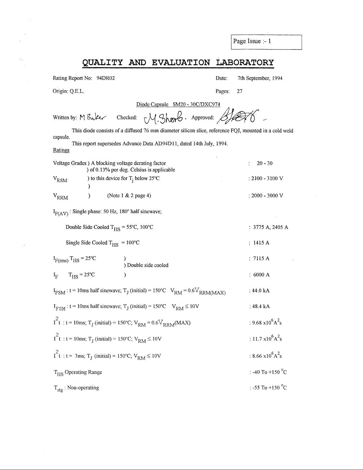
Rating Report
Origin: Q.E.L.
by:
Written
capsule.
Ratings
Voltage
V
RRM
IF(A
M
This diode consists of a diffused
This report supersedes Advance Data AD94Dll, dated
Grades) A blocking voltage derating factor
V)
: Single phase:
Double
QUALITY
No:
94DR02
gJA.,r
) of
0.13% per
to
this device for Tj below
)
)
) (Note 1 & 2 page
50
Hz,
Side Cooled T
AND
Checked: cf{
deg.
180°
=
55°C,
HS
EVALUATION
Diode Capsule
.<3~'
76
mm diameter silicon slice, reference FQJ, mounted
Celsius is applicable
25°C
4)
half sinewave;
100°C
SM20
- 30C/DXC974
Approved:
14th
July,
LABORATORY
Date: 7th September,
Pages:
27
~
1994.
:
2100 -3100
: 2000 - 3000 V
:
3775
20
.-
in
-30
A,
1994
a cold
2405
weld
V
A
Single Side Cooled T
I
: t = lOms halfsinewave; TJ (initial) =
FSM
I
: t = lOms halfsinewave; T
FSM
2
It:
t =
10ms;
TJ (initial) =
2
It:
t =
10ms;
TJ (initial) =
2
It:
t =
3ms;
TJ (initial) =
T
HS
Operating
T
: Non-operating
stg
Range
HS
150°C;
150°C;
150°C;
=
100°C
) Double side cooled
)
150°C
(initial) =
J
V
V
V
RM
RM
RM
150°C
= 0.6V
::;
lOV
::;
lOY
V
= 0.6V RRM(MAX)
RM
VRM::;
~MAX)
lOY
1415
:
:
7115
:
6000
:
44.0 kA
: 48.4 kA
: -40
To
:
-55
To
A
A
A
+150
+150
°c
°c
Page 3
-2-
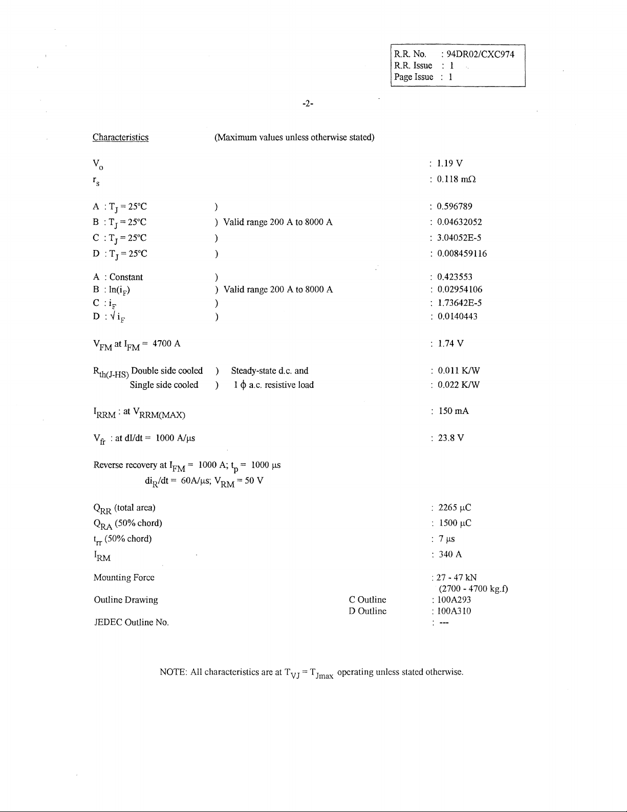
R.R. No. :
R.R. Issue 1
Page Issue : 1
94DR02/CXC974
Characteristics
A
:T
=2SOC
J
B : TJ=25°C
C : T
= 25°C
J
D : TJ=25°C
A : Constant
B : In(iF)
C : iF
D
:"
iF
V
at
IFM
FM
~(J-HS)
I
RRM
= 4700 A
Double side cooled )
Single side cooled )
:
at
VRRM(MAX)
(Maximum
) Valid range 200 A to 8000 A
)
) Valid range 200 A to 8000 A
)
values unless otherwise stated)
)
Steady-state d.c. and
1
<l>
a.c. resistive load
V
1.19
mn
0.118
: 0.596789
: 0.04632052
: 3.04052E-5
: 0.008459116
: 0.423553
: 0.02954106
1.73642E-5
0.0140443
1.74 V
: 0.011 KIW
: 0.022 KIW
150mA
V fr :
at
dIldt = 1000
Reverse recovery
diR/dt =
Q
(total area)
RR
Q
(50% chord)
RA
~
(50% chord)
IRM
Mounting Force
Outline
Drawing
JEDEC Outline No.
Nf!s
at
IFM = 1000 A; tp = 1000
60Nf!s;
NOTE:
V
=
RM
All characteristics are
50
f!s
V
C Outline
D Outline
at
TV J = T Jrnax operating unless stated otherwise.
23.8 V
: 2265).l.C
1500
!lC
: 7
f!S
: 340 A
: 27 - 47 kN
(2700 - 4700 kg.I)
: 100A293
: 100A31O
Page 4
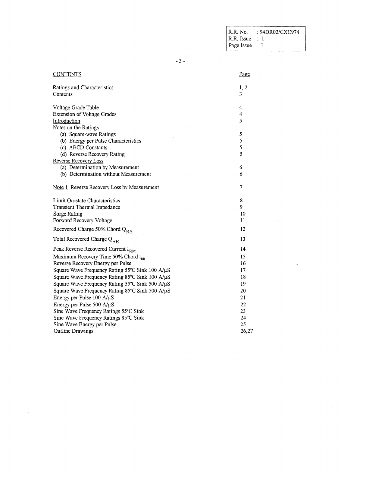
CONTENTS
- 3 -
RR
No.
: 94DR02/CXC974
RR
Issue 1
Page Issue : 1
Ratings and Characteristics
Contents
Voltage Grade Table
Extension of Voltage Grades
Introduction
Notes on the Ratings
(a)
Square-wave Ratings
(b) Energy per Pulse Characteristics
(c)
ABCD
Constants
(d)
Reverse Recovery Rating
Reverse Recovery Loss
(a)
Determination by Measurement
(b) Determination without Measurement
Note I Reverse Recovery Loss by Measurement
Limit On-state Characteristics
Transient Thermal Impedance
Surge Rating
Forward Recovery Voltage
Recovered
Total Recovered Charge Q
Peak Reverse Recovered Current
Maximum Recovery Time 50% Chord
Charge 50% Chord Q
RR
RA
IRM
tRR
Reverse Recovery Energy per Pulse
Square Wave Frequency Rating
Square Wave Frequency Rating
Square Wave Frequency Rating
Square Wave Frequency Rating
Energy per Pulse
Energy per Pulse 500
100
AJ).lS
AJ).lS
Sine Wave Frequency Ratings
Sine
Wave
Frequency Ratings
Wave
Sine
Energy per Pulse
55°C
85°C
55°C
85°C
55°C
85°C
Sink
Sink
Sink 500
Sink 500
Sink
Sink
100
100
Outline Drawings '
A/).lS
AJ).lS
A/).lS
AJ).lS
1,2
3
4
4
5
5
5
5
5
6
6
7
8
9
10
11
12
13
14
15
16
17
18
19
20
21
22
23
24
25
26,27
Page 5
-4-
RR
No. : 94DR02/CXC974
RR
Issue
: 1
Page
Issue
: 1
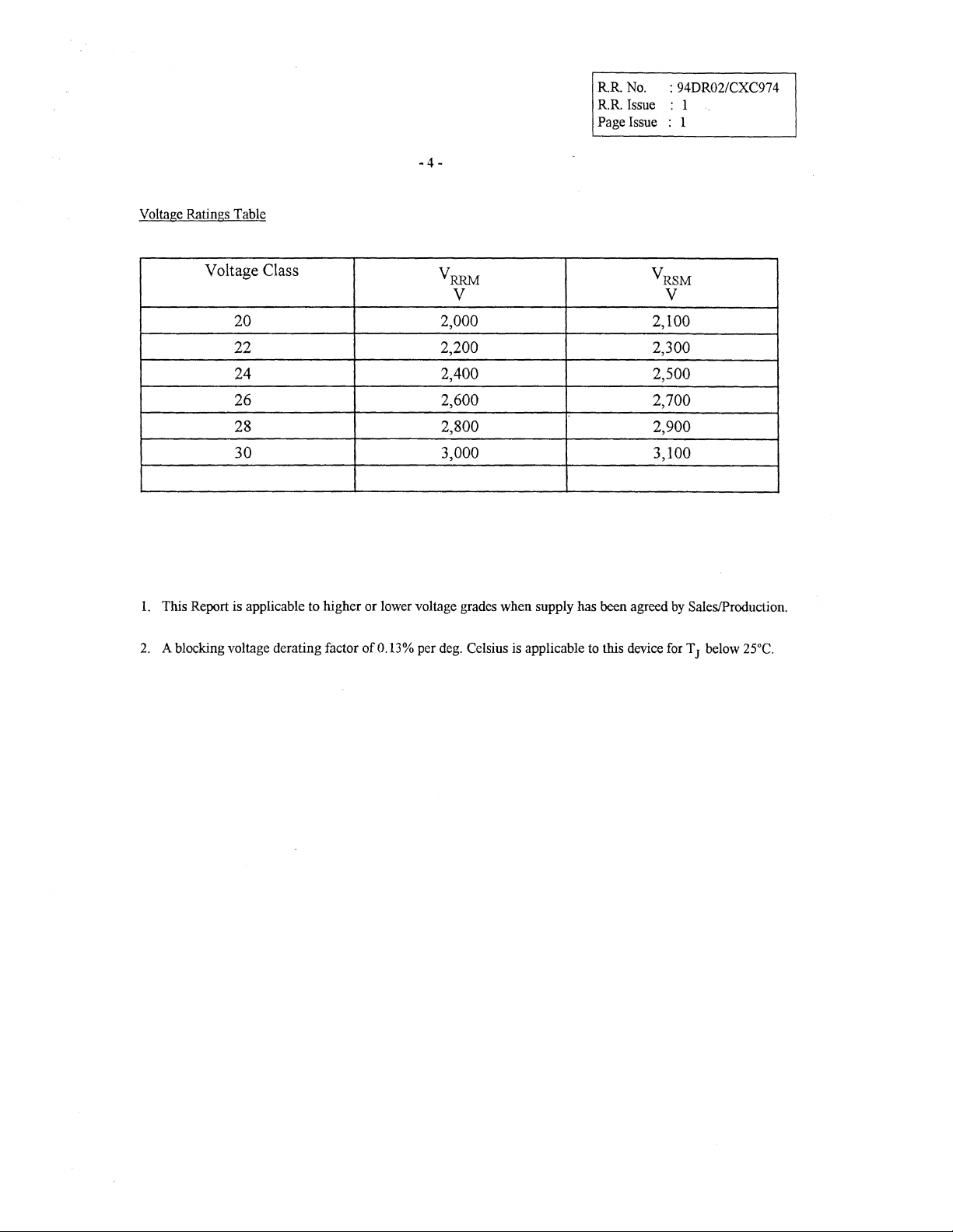
Voltage
Ratings Table
Voltage Class
20 2,000
22 2,200 2,300
24 2,400
26 2,600
28 2,800 2,900
30 3,000 3,100
1.
This
Report
is
applicable to higher
2.
A blocking voltage derating factor
or
lower
of
0.13% per
V
RRM
V
V V
2,100
2,500
2,700
voltage grades when supply has been agreed
deg.
Celsius is applicable
to
this
device
RSM
by
SaleslProduction.
for
TJ below
25°C.
Page 6
INTRODUCTION
- 5 -
R.R
No.
: 94DR02/CXC974
RR
Issue : 1
Page Issue : 1
This diode series comprises fast recovery capsule devices with all diffused silicon slices. All these diodes
controned reverse recovery characteristics with good "K" factors,
applications.
NOTES
frequency ratings.
in
expression for
ON
TIlE
RATINGS
(a) Square wave ratings
are
These ratings
(b) Energy
These curves enable rapid estimation
Let:
Hertz. Let R
Ep
per
be
TSINK = TJ(MAX) - (Ep *
(c) ABCD Constants
These constants (applicable only over current range
the
givcn for leading edge linear rates
pulse characteristics
of
device dissipation
the
Energy
per
pulse for a given current and pulse width,
thl-HS
be
the steady state d.c.
i*
forward characteristic given below:
Rthl-HS)
thennal
resistance (junction to heat sink).
and
are
of
rise
offorward
to
be obtained for conditions
of
V F characteristic
particularly suitable for use
current
of
100
and
500 AiIlS.
not
covered
in
joules. Let f
on
page 8)
be
the repetition rate,
are
the coefficicnts
in
free-wheel
by
have
the
of
..
the
Vj
= A + B.
(d) Reverse recovery ratings
(i)
Q
is based
RA
In
on
(i
50%
j)
+
C.
i j + D.
IRM
chord
r---------------------------------------~
Jif
as
shown below.
: whcre
iF
= instantaneous forward current.
Page 7
-6-
R.R.
No. : 94DR02/CXC974
R.R.
Issue
: 1
Page
Issue
: 1
(ii) Q
(iii) K factor =
Reverse
The
(a)
From
present
waveform
this
is
RR
i.e.
Recovery
following
Detennination
waveforms
during
recovery,
be
TSINK(new) = TSINK(original) - E * (k+
where
k =
0.287
E = Area under
f=
Rated
frequency
Rthl-HS
The total dissipation
=
based
on
a
150
llS
150llS
QRR
= J
iRR.dt
t=O
~~
Loss
procedure
E joules per
reverse
d.c.
is
recommended
by
measurement
of
recovery
an instantaneous reverse
pulse.
(K/W)/s
loss
waveform
in
Hz
at
the
thermal resistance (KIW)
is
now
given
integration
current obtained
A new sink temperature
original sink
by
time
for
per
pulse
W(tot)
use
where it
from
recovery
in
joules
temperature.
= W(original) + E * j
is
a high
loss
can
(W.s.)
necessary
frequency
waveform
then
be
i*
Rth(J-HS»)
to
include
shunt (see
must
be
evaluated
reverse
recovery
Note
1) and
constructed.
from:
reverse
Let the
loss.
area
voltage
under
(b) Determination without
In
circumstances
the additional
Let E be
Let f
then TSINK(new) = .TSINK(Original) - (E *
where
temperature
A suitable
to
a peak
of
Grade,
losses
the
value
be
the operating
T SINK(new)
given
with
R-C
snubber
value
(VRM) of
the
reverse
E injoules
loss
where
of
energy
frequency
is
the
the
frequency
network
0.67
may
MeaSurement
it
is
not
possible
may
be
per reverse
in
Hz
required maximum heat sink temperature and T SINK(original)
ratings.
is
connected
of
the
maximum
be
approximated by a
to
estimated
cycle
across
grade.
curves.
measure
as
in joules
voltage
follows.
(curves
i*
Rth)
the
diode
If
a different
pro
rata adjustment of the
and current
on p 16
to
restrict
grade
conditions,
).
the
transient
is
being used
maximum
or
for
reverse
or
V
RM
value
design
is
the
voltage
is
other than
obtained
purposes,
heat sink
waveform
0.67
from
the
Page 8
NOTE
Reverse
This
care
must
(a)
forward
I
Recovery
device
a.c.
Loss
has a low
be
taken
to
ensure that:
coupled devices such
current.
by
Measurement
reverse recovered charge
as
current transformers are not affected
and
-7-
peak
reverse
RR
No.
RR
Issue
Page
Issue
recovery
current.
by
prior passage of high amplitude
When
: 94DR02/CXC974
1
: I
measuring the charge
(b) A suitable, polarised, clipping circuit
overloading the internal amplifiers
(c)
Measurement of reverse
2.2
ohms
connected across diode anode
by
recovery
must
be
connected
to
the input of the measuring
the relatively high amplitude forward current signal.
waveform
to
cathode.
should
be
carried out with an appropriate
oscilloscope
snubber
of
to
avoid
O.5uF,
Page 9
Page
..
Page
.RR
RR
No.
Issue
No.
Issue
8
1
94DR02
1
10000
CJ)
-
Q)
....
Q)
0-
E
$
.....
c
Q)
....
....
:::J
(,,)
-e
ro
~
0
u..
CJ)
:::J
0
Q)
C
ro
.....
c
ro
.....
CJ)
C
1000
Forward
V
J
/
7
1500C/
V
/
/
I
.
..
Characteristic
V·'
.
:/
J
,
,
,
~
/
,/
.
.
~
,
I
250C
V'"
.
of
Limit
Device
':?'
~
V
/
150°C
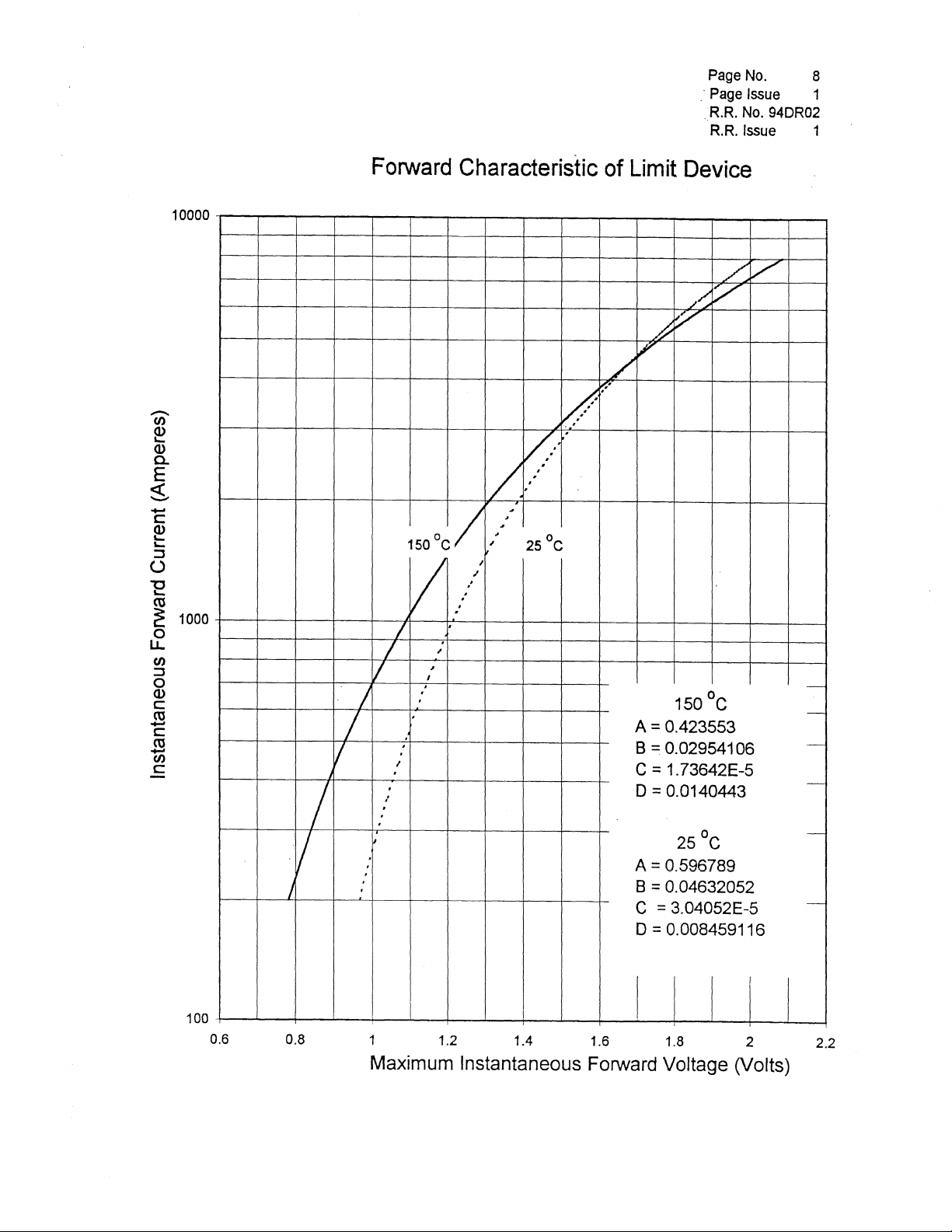
A = 0.423553
B = 0.02954106
C =
1.
73642E-5
0::: 0.0140443
~
V
/~
'/
-
-
.-
-
100
0.6
II
)
0.8
I
25°C
J
I
.
1 1.2 1.4 1.6 1.8 2 2.2
Maximum Instantaneous Forward Voltage (Volts)
A::: 0.596789
8::: 0.04632052
:::
3.04052E-5
C
0=0.008459116
I
I
-
-
I
Page 10

Transient
Thermal
Impedance
(Junction
to
Heat
Sink)
0.1
0.01
~
'-"
OJ
()
c
ro
-0
OJ
a.
E
ro
E
L-
0.001
OJ
..c
I-
0.0001
0.001
--'-
-.-
-_.
--
--
/
L_
V
.-
-_
...
0.022
KJW
S.S.C
0.011
D.S.C
KJW
..,.,/
/""
......
-
:,..-
....
~
v
v
"......,
-
-
!-"
1'
--
V
.....
~
.......
)
.........
V
......
1--'
,/
v
/
--
I
0.01
0.1
Time (Seconds)
1
10
100
:;u
:u
~
C
(l)
::0
~
Z
p
<D C
~
0
;:u
0
N
"0
II)
<0
CD
~
(l)
.....
<0
"U
I»
(l)
Z
0
<D
Page 11

1.00E+()6
Maximum
@
Initial
-
Non-Repetitive
Junction
Temperature
Surge
Current
150°C
2
tVRRM
,
=1DV _
<t;
...
c 1.00E+05
Q.)
~
...
~
...
Vl
::J""
U «
Q.)0')
OJ
0
... ,...
::J
0
C/) -
Q.)
""-
.S
E
C/)
:::J
!t:
E
ro
.-
:r:
~
..¥:
:2
ro
~
Q.)
0.
I-
ro
....
o
100E+04
1.00E+03 1
t::-..
~-..
-..
.................
--
-
-
f-"
---
-
--
3
Duration of Surge (ms)
............::
::::--.
~
l.--
.......
5
b:'1---
_
....
10
::::-
......",
-
~
~
-....:
::::::
~I---
v
./
/'
v"
V
Duration
./
..,/
./
/'/
~
1--'1--'
i.-'
5
of
Surge (Cycles @ 50 Hz)
::::::::::::
10
./
./
~
/'
r-
./
IL
v v
.:::::
::::
,2t:6D%VRRM
I--
-~
::::1--
50
..
~
100
'FSM:VRRM=1DV
'FSM:6D%VRRM
- -
;;0
::u
ii
c
CD
;;0
•
;0
z
0
<0
.:>0.
0
;;0
0
I\)
-0-0
II)
coco
CD
-z
!:l 0
c:
CD
...
II)
CD
0
Page 12

100
...-
en
......
~
Q)
0>
co
......
"0
>
10
~
Q)
>
0
0
Q)
a::
"0
'-
V
L
V
Forward
V
V
V
/
Recovery
(Maximum
/'
j.;'
j.;'
V
/
V
/
V
V
V
V
V
Voltage
Peak)
L
/
V
V
150°C
I
25°C
Page
..
Page
RR.
R.R.
I
Issue
No.
Issue
11
1
94DR02
1
--
~
0
u..
1
100
I
Applied Ramp Rate (AI'tls)
I
1000
I
10000
Page 13

Page
..
Page
RR.No.
RR.
No
Issue
Issue
12
1
94DR02
1
10000
(])
~
co
..c:
o
"0
~
(])
>
o
()
(])
0:::
Maximum
@150
Recovered
°c
Junction
Charge
Qra
Temperature
V
50 % Chord
4000 A
I I
2000 A
~
~
1000 A
V
1000
10
IV
/v
I
v~
~V
V
~
lfv
vV'
VV'
V
[;:v
~
I
Commm~tion
~
V
V
,
Rate
V
/
V
(A/'tJ.s)
/
V
I I
600 A
I I
400 A
I
I
1000
Page 14

-Page
-
Page
RR
RR
No.
Issue
No.
Issue
13
1
94DR02
1
10000
-
U
:::t
'-"
(J.)
e>
ro
..c
U
u
~
(J.)
>
8
(J.)
0::
Maximum
150
,/
t/
Total
DC
Junction
~
/
/
V
/
V
V
Recovered
Temperature
~
~
V
v
V-
V
v
V
Charge
Qrr
V
/
,V
V
V
V
/'
V
V
@
4000 A
I I I
2000 A
1000 A
600 A
400 A
I
I
..
1000
10
V
I
Commutation
100
Rate
(AJ~s)
I
i
1000
Page 15

Page
:
Page
RR.
R.R.
No.
Issue
No.
Issue
14
1
94DR02
1
.........
Ch
~
Q)
c.
E
$
.:E
a::::
.....
c:
~
...
::J
U
~
(1)
>
0
(J
Q)
c:::
Q)
en
...
Q)
>
Q)
c:::
10000
1000
Maximum
@ 150°C
/ /
~
~
V
~
V
Peak
Junction
)/
v
'/
'/
~
V
Recovered
Temperature
§
7/
77
~7/
1/7'
V
Current
6
A
.7/
W V
/
l.7'
V
IRM
2000 A
1000 A
SOOA
400 A
I I
I I
200 A
100
10
100
Commutation Rate diR/dt (AlJls)
1000
Page 16

Maximum Recovery Time trr
Page
..
Page
R.R.No.
R.R.
No
Issue 1
Issue 1
15
94DR02
10
@150
°c
Junction Temperature, 50% Chord
~
~
~
~
i'(
"'
~)o..
~
~
......
I'
~
~
"-
.::::
~
I'-.
~
~
~,
~
~
t'(
~
R
'"
~
4000 A
2000 A
I I
1000A
I I
SOOA
I I
400
A
-
1
10
Commutation Rate (AlJls)
100
100(
Page 17

Page
. Page Issue 1
.
R.R.
.
R.R.
Maximum Reverse recovered Energy Loss Per Pulse
ER
@
150°C
Junction Temperature
16
No.
94DR02
Issue 1
-g
a.
.....
-g
ID
"S
o 0
-,
'-'Q)
(l)
.:.::
fJ)
-
:::J
n..c
r...
-
(l)
.-
n.
>-
.....
C>
r...
(l)
C
W
.0
.....
w
(5
z
10
a.
«I
Q)
C)
«I
~
~
0
...
«I
Q)
a.
~
«I
~
0
'-
a.
Q)
o
a:::
Q)
Snubber 0.5
1
/-IF
L
~
:/
V
& 2.2
V
V
~
.....
V
/
V
./"
n.
i"
./
V
VRM
V
f'
,,/
i-"""
,,/
.....-
=0.67 Voltage Grade
t::::
,..,
r'
,..,
v
,,'/
./
,,"'"
V
./"
/"
/"
/'
/
~
.,,-/
/"
V
L
/"
/'
V
.....
./
2000 A
1000A
I
I
600 A
II
I I
300A
0.1
_.
10
I
i
100
Commutation Rate (A/)ls)
I
100C
Page 18

Frequency vs Pulse Width
. Page
.
Page
RR
RR
No.
Issue
No.
Issue
17
1
94DR02
1
:g
Q)
:c
---
~
c
Q)
:::J
0"'
~
lL.
1.0E+05
1.0E+04
1.0E+03
1.0E+02
"
"
"
~
"
"
Heat
i'.
"
!'..
Sink Temperature 55°C, di/dt 100
r--..r--..
....
6
kA
~
8
'-
kA
10
~
"
'\
kA
\
~
~
~
R
"\
~
100 % Duty Cycle
II
I
I,
~
f'.
I"
r-..
f\
r-..l\l'
"'-
"-
"
" "
I'
i\
l'\
"
,,"-
" "
f"-
.".
l'..
i'."
~'"
t\.."
'"
"
~~
AI'tlS
~
"
"-
i'\
'"
I\.
I\.
"
"
r\:
"
i',1'\
I\.
1'\
K
I'\:
1\
i\. r\
1\
1.0E+01
i.0E-OS
1.0E-04 1.DE-03
Pulse Width (Seconds)
~
1.0E-02
Page 19

Frequency vs Pulse Width
. Page
.
Page
RR
R.R
No.
Issue
No.
Issue
18
1
94DR02
1
1.0E+05
1.0E+04
~
<J.)
J:
-
~
c:
<J.)
1.0E+03
::J
0-
~
U.
"
"'
"-
['\.
"
Heat Sink Temperature 8SoC, di/dt 100
"\,
"\,
I'
"
~
'f',
"
"-
6kA
'-
\:
"
'\.
"-
8kA
'\
'"
\
10kA~
'"
. 1 00 % Duty Cycle
r7
/
,
~
~
~
~
" "
"
"
"
'-
" K
"
~~
'\
\
/
~
"
""
'-'-
"\."
'"
~~
'"'"
~~",
'\
~
~
i\.
A/J.lS
~
~
1.0E+02
1.0E+01
1.0E-OS
~
1.0E-04 1.0E-03
Pulse Width (Seconds)
"'
1']\
~
~
~
K
'\
1\
i\
"-
1'1'.1'
'"
1\
f\
4kA
'"
1\
1\
I'
I'
~
1.0E-02
Page 20

Frequency vs Pulse Width
Page
Page
R.R.
No. 94DR02
R.R.
Issue 1
No.
Issue 1
19
1.0E+OS
1.0E+04
~
Q)
:r.:
'-'
()'
c:
Q)
1.0E+03
::J
0-
~
U.
1.0E+02
"-
"-
4kA
~
"
f----6kA
Heat Sink Temperature
"-
"
"'\.
10
~
"-
,
~
I'...
kA
"-
r-..
"
~
i'..
"-
.....
'\
"
"'
~
"-
"-
"'- "'-
" "
"
,"
I'
8kA
"'"
I
I"
,"'\.
,~
,
~
"
~
"-
"
"
"
SSoC,
100 % Duty Cycle
I
di/dt 500
II
I,
I'\.
'\
~
,
\,
'-
'\
"-
"
"-
"-
"'-"
i"-i\..
"
"-
,,"'\.
"'-
~
1"'-
.~
,
"-
'\.
"'-~
,'"
"
'\
'\
Af't-lS
"'\.
~
r'\.
"-
"
'\
i'..
"
"- "-
"-
'"
'\
'\
i'.~
I"-
I'\.
i\
1\
I\.
\
1.0E+01
1.0E-05
I
1.0E-04 1.0E-03
Pulse Width (Seconds)
i\
I
!
1.0E-02
Page 21

~
c:
~
0-
~
u..
1.0E+OS
1.0E+04
1.0E+03
1.0E+02
"-
,
,
4kA
1-----6
Heat Sink Temperature 85°C, di/dt 500 A/JlS
"-
f'..
"'-
"
",,"
kA I'..
"'-
"
" "-
8kA~
"
I"-
10 kA
'\
Frequency vs Pulse Width
f'.
"-
I,
I"
r--..
r'\"
i'.
"
'-
1"..,
I'
"
r'\
I\.
1'-..
1\"
1"-1"-
"'-
"
~~~
........
"
~
"
~~
"
"-
~
S
"- "-
100 % Duty Cycle
,
~
l\..
~
'""
~
"-
'-
II
r'\
'~~
"
I'
i'..
"
"
K
"-
"'-,
r7
'-
"
"
'\
K
"''''
1")1.
~"
r-...."'-
"-
~
Page
No.
Page
Issue
RR
No.
RR
Issue
l'(
"-
~
"-
~
I'\.
~
~
~
'\.
i'.
l"\
"
l\. 1\
'\.
'\.
"
1\
20
94DR02
I"
l'
f'
1'1'
l'\
I"
I"
[\
1\
1\
1
1
I'
1\
r'I
1.0E+01
1.DE-OS
1.DE-04 1.0E-03
Pulse Width (Seconds)
11\
1.DE-02
Page 22

Energy vs Pulse Width
Page
Page
RR
RR
No.
Issue
No.
Issue
21
1
94DR02
1
Q)
C/)
:::l
c:.
'-
Q)
c.
C/)
~
::J
o
-,
-
>-
~
~
ill
1.0E+03
1.0E+02
1.0E+01
1.0E+OO
Junction Temperature 150
V
/ /
V
,/
/
v
/
/
V
./
/
7
/
"'
/"
/
i/"
/'
17
V
/
,
°e
I..-
i.I
......
1.0-
"'
~lo;'
I?
di/dt 100
/ V
/
7
v v
/'
V/"'
V
V
0
./
./
/
A/J.lS
1/
/
I/v
'/
/
./
~
./
~
v
V
"",v
;-
~
;-~
~
./
./
"
v
10
8k.A
6kA
4kA
2kA
k.A
1.0E-01
1.0E-02
1.0E-05
II
V
V
/
1.0E-04 1.0E-03
1.0E-02
Pulse Width (Seconds)
Page 23

."Page
Page
R.R
RR
No.
Issue
No.
Issue
22
1
94DR02
1
CD
-
!!l
::J
Cl.
L-
CD
C.
(/)
~
:::J
o
...,
--
>-
E>
~
W
1.0E+03
1.0E+02
1.0E+01
1.0E+OO
1.0E-01
Energy
Junction
Temperature
//
[,77/
i;'
"'i;'~
l/
......
L
.,.
/'
;'
V
/'
.........
./
.."
./
/
,/
......
L
./
./
~V/
~
/"
7
.....
1.-
l/
/
.;,.
./
/"
V /
V
V
......
......
vs
......
V /
V
Pulse
150
i;"
v
i;"
./
......
......
/
V
'"
I-."r
V
/
Width
°e,
di/dt
./L
V/./
......
)'''
v.....
......
/'
/'
vV
500
./
/
v/
V
V
./
./
A/Ils
.,.
./
V
/'
V
l/~
;'
;'
/
/
)/
10
kP
i;'
~
.....
1,.0
8kP
8kA
4kA
2kA
.....
V
.....
/
~
~
l/
V
P
v
1.0E-02
1.0E-05
1.0E-04 1.0E-03
Pulse Width (Seconds)
1.0E-02
Page 24

Page
No.
Page Issue 1
R.R.
No. 94DR02
R.R.
Issue 1
23
1.0E+OS
1.0E+04
~
Q)
::r:
---
~
C
Q)
1.0E+03
::::J
0-
~
U.
1.0E+02
4kA
6kA
akA
10 kA
I'\.
-"--
~
"'"
"
r---
---
--
Heat
r'\.
"
r--.
~
--..
r-..
~
---
~
,
..........
-
Frequency
Sink
1\
......
t'-
......
Temperature
i'r--.
,
......
r-....
f'...
,
'-..."
"
""-"
'"
vs
~
~
~
"
"
Pulse
Width
5SoC,
100 % Duty Cycle
1/
II
,
~
~
"
~
"-
~r--.
"'-
I
I
Sine
'"
"
""
"
''"
'"
Wave
0-.
1,\
"
""
..
~
l'-.
1'\
"'-
i'-
"\
~
I'\.
i'\
~i'\
"
1.0E+01
1.0E-05
1.0E-04 1.0E-03
Pulse Width (Seconds)
1.0E-O~
Page 25

: Page
No.
Page
Issue 1
R.R.
No.
R.R.lssue
24
94DR02
1
1.0E+OS
1.0E+04
~
CD
:E:
........
~
C
~
1.0E+03
W
u..
1.0E+02
4kA
6kA
8kA
,
"
"-
r--...
"
r----
r---
10
kA
f'..
~
-......
r---....
I""'-
-
Heat
"
i'\.
"
r......
'"
I'...
r---...
Frequency
Sink
,r--..~
"
,.....
r--.
Temperature
"-
"-
......
,
"-"-
"
"-
"\."
~
"-
1""-
"
.....
vs
~
~
~
'"
""
Pulse
8SoC,
. 100 % Duty Cycle
1/
!/
~
~
~
'"
~
"
"-
"
~,
"
.....
.....
Width
Sine
"-
"
"-"-
~
'-
" '"
",,-
"
Wave
~
"-
~
R
"-
I"-
I~
I\.
['...
"-
~
f'
"'
'\
1'\
l\
"-
I'f'I,
I'
I'
~
1.0E+01
1.0E-OS
1.0E-04 1.0E-03
Pulse Width (Seconds)
"
'"
1.0E-O~
Page 26

.
Page
Page
R.R
RR
No.
Issue
No.
Issue
25
1
94DR02
1
..-
Q)
!!2
::J
0;.
'-
Q)
0-
U)
Q)
::J
a
...,
--
>-
e>
~
UJ
1.0E+03
1.0E+02
1.0E+01
1.0E+OO
1.0E-01
~
~
~
Junction
f.-"
.-
V
....-
vf'
.,,-
,/
-
.",
~,....
~
V
v
1.'/
,/
./
Energy
vs
Temperature
/'
/'
V
/
~
~~
....
./
./
L
V
V
/
V
V
V
v /
i-"
/'
/
Pulse
150
./
/
/
1/
./
/
)/
V
v"""
IL
./
Width
DC,
,,;~
~
1/
./
/
~
/
,,;,r
~
Sine
/
./
./
./
/
Wave
V /
/'
/
V
V
V
/
./
,r
/
,r
10
k.A
~
8kA
./
/
/
/
v
1//
./
/
./
/'
..
,,;
",/
6kA
4kA
2kA
.
1.0E-02
1.0E-05
------
I
I
1.0E-04 1.0E-03
Pulse Width (Seconds)
I
I
I
I
1.0E-02
Page 27

§
INTERNATIONAL
~
G.A.
If)
g§
I-
~
5
~
~
)5
§
DWG
WEIGHT.
FINISH.
DEVICE
CENTRE
DISTRIBUTED
SURFACES
CLAMPING
MOUNTING:
LINE
OUTLINE
No.
1598100H601
1.7kg
NICKEL
OF
OVER
TO
WHICH
FORCE
No.
PLATE
CLAMPING
LOCATION
AREA
DEVICE
FORCE
HOLES
OF
CONTACT.
IS
TO
BE
AND
BE
FLAT
CLAMPED
EVENLY
TO
= 3700±1000kgf. (37±10kN)
-
26
APPLIED
Tal.
ON
BE
0.04
-
ON
WIDE.
CXC974
.CXC15C
CXC18C
CXC20C
CXC21
C
CXC26C
CXC30C
~~------------------------------------~----------------------~
~
z
o
Vi
If)
~
ffi
a.
¢3.6/3.5x3
DEPTH
IN
IN
2-HOLES.
CATHODE
ANODE.
MIN.
AND
ONE
ONE
~
~
--G}--
UNCONTR
~LlED
COP
to
r<)
'--,
L()
<..0
r---
r<)
0
W
U1fU1
I
W'-'
0:::
_
o-w
:::i!I
0
u
o
r
,
MIN
t
t
L 0.8
MIN
P.O.
S
1-
J
)
)
)
I
..
Cl
to
WESTCODE
BOX
57, CHIPPENHAM,
¢73.1
±0.1
"'1.
l
(
(
(
J
¢73.1
±O.1
SEMICONDUCTORS
WILTSHIRE,
-I
SN15
DWG
UL.
•
'CREEP
OVER
CONVOLUTIONS
=
No.
100A293
LTD
..
ENGLAND.
41.5
PATH
MIN.
Page 28

~
INTERNATIONAL
~
G.A.
DWG
~
WEIGHT.
~
FINISH.
6
DEVICE
~
CENTRE
IX
DISTRIBUTED
~
SURFACES
~
CLAMPING
~~------------------------------~--------------------~
u..
0
z
0
Vi
Vl
:i
0::
\oJ
~
Z
MOUNTING:
LINE
OUTLINE
No.
159B100H661
1.2kg
NICKEL
OF
LOCATION
OVER
TO
WHICH
FORCE
No.
-
PLATE
CLAMPING
AREA
DEVICE
FORCE
HOLES
OF
CONTACT.
IS
TO
BE
AND
BE
FLAT
CLAMPED
APPLIED
EVENLY
TO
= 3700±1000kgf. (37±10kN)
27
TOL.
BE
ON
0.04
-
ON
WIDE.
DXC974
.OXC15C
DXC18C
DXC20C
DXC21
C
DXC26C
DXC30C
~3.6/3.5x3
DEPTH
IN
CATHODE
IN
ANODE.
MIN.
2-HOLES,
AND
ONE
ONE
~
~
w
j;
j;
x
~
«
I-
:::E
~
(j
Q
IX
~
Vl
0
\oJ
CD
I-
0
Z
>-
4:
~
Z
0
F
4:
~
0::
e
!1;
IJl
0
..-
..-
"Q
---e----
;E
COMPRESSED
g
HEIGHT
~
8
0.8
MIN
g-H
[w
·;L~t~~.B
!:!]
C'J
~
~
;;
0.8 • ...
MIN
P.O.
BOX
I
WESTCODE
57,
CHIPPENHAM.
~73.1
•
±0.1
~73.1
I
±0.1
SEMICONDUCTORS
WILTSHIRE.
SN15
lJL,
..
,
LTD.,
ENGLAND.
+
'"
CREEP
OVER
COVOlUTIONS
= 25.4
PATH
MIN.
Page 29

Drawing Number – W42
Outline Number – 100A310
Weight 1200g
Westcode Customer Services email: wsl.sales@westcode.com Telephone: +44 (0)1249 444524 Fax: +44 (0)1249 659448
Page 30

Drawing Number – W7
Outline Number – 100A293
Weight 1700g
Westcode Customer Services email: wsl.sales@westcode.com Telephone: +44 (0)1249 444524 Fax: +44 (0)1249 659448
 Loading...