

Datasheet M37540M4-XXXSP, M37540M4-XXXGP, M37540M4-XXXFP, M37540E8SP, M37540E8GP Datasheet (Mitsubishi)
...Page 1
PRELIMINARY
Notice: This is not a final specification.
Some parametric limits are subject to change.
MITSUBISHI MICROCOMPUTERS
7540 Group
SINGLE-CHIP 8-BIT CMOS MICROCOMPUTER
DESCRIPTION
The 7540 Group is the 8-bit microcomputer based on the 740 family
core technology.
The 7540 Group has a serial I/O, 8-bit timers, a 16-bit timer, and an
A-D converter, and is useful for control of home electric appliances
and office automation equipment.
FEATURES
Basic machine-language instructions....................................... 71
•
The minimum instruction execution time .......................... 0.50 µs
•
(at 8 MHz oscillation frequency for the shortest instruction)
Memory size ROM ............................................16K to 32K bytes
•
Programmable I/O ports ........................................................... 29
•
Interrupts .................................................. 15 sources, 15 vectors
•
Timers ............................................................................ 8-bit ✕ 4
•
Serial I/O1 ...................................................................... 8-bit ✕ 1
•
Serial I/O2 ...................................................................... 8-bit ✕ 1
•
A-D converter ................................................ 10-bit ✕ 8 channels
•
Clock generating circuit ............................................. Built-in type
•
RAM ..............................................512 to 768 bytes
(25 in 32-pin version)
(14 sources, 14 vectors for 32-pin version)
16-bit ✕ 1
(UART or Clock-synchronized)
(Clock-synchronized)
(6 channels for 32-pin version)
(low-power dissipation by a ring oscillator enabled)
(connect to external ceramic resonator or quartz-crystal oscillator
permitting RC oscillation)
Watchdog timer ............................................................ 16-bit ✕ 1
•
Power source voltage
•
XIN oscillation frequency at ceramic oscillation, in high-speed mode
At 8 MHz ....................................................................4.0 to 5.5 V
At 4 MHz ....................................................................2.4 to 5.5 V
At 2 MHz ....................................................................2.2 to 5.5 V
XIN oscillation frequency at RC oscillation
At 4 MHz ....................................................................4.0 to 5.5 V
At 2 MHz ....................................................................2.4 to 5.5 V
At 1 MHz ....................................................................2.2 to 5.5 V
Power dissipation ............................................ 25 mW (standard)
•
Operating temperature range ................................... –20 to 85 °C
•
(–40 to 85 °C for extended operating temperature version)
APPLICATION
Office automation equipment, factory automation equipment, home
electric appliances, consumer electronics, car, etc.
Note: Serial I/O2 can be used in the following cases;
(1) Serial I/O1 is not used,
(2) Serial I/O1 is used as UART and BRG output divided by 16 is
selected as the synchronized clock.
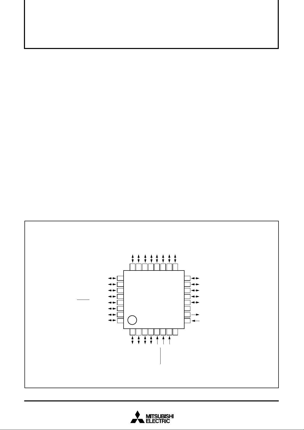
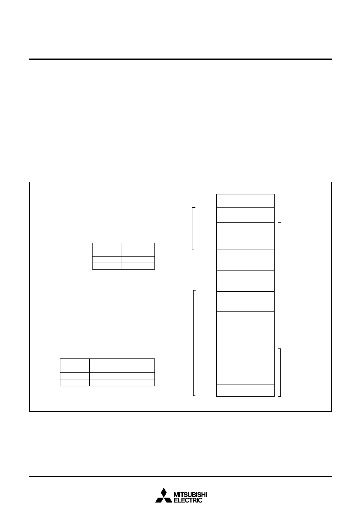
PIN CONFIGURATION (TOP VIEW)
P0
7
P12/S
P13/S
P10/RXD
P11/TXD
CLK1/SCLK2
RDY1/SDATA2
P14/CNTR
P20/
P21/
AN
AN
1
1
0
0
1
OUT
/TX
5
P0
23
2
3
/AN
3
P2
4
P0
22
3
4
/AN
4
P2
3
P0
21
4
5
/AN
5
P2
6
P0
24
25
26
27
M37540M4-XXXGP
28
29
30
31
32
M37540E8GP
1
2
/AN
2
P2
OUT
OUT
/TY
/TZ
1
2
P0
P0
201718
19
7
6
5
REF
V
RESET
1
0
/INT
/CNTR
7
0
P3
P0
8
SS
CC
V
CNV
16
15
14
13
12
11
10
9
P34(LED4)
3
(LED3)
P3
2
(LED2)
P3
P3
1
(LED1)
0
(LED0)
P3
SS
V
X
OUT
X
IN
Package type: 32P6B-A
Fig. 1 M37540M4-XXXGP, M37540E8GP pin configuration
Page 2
PRELIMINARY
Notice: This is not a final specification.
Some parametric limits are subject to change.
MITSUBISHI MICROCOMPUTERS
7540 Group
SINGLE-CHIP 8-BIT CMOS MICROCOMPUTER
P12/S
P13/S
CLK1/SCLK2
RDY1/SDATA2
P14/CNTR
P20/AN
P21/AN
P22/AN
P23/AN
P24/AN
P25/AN
P26/AN
P27/AN
V
REF
RESET
CNV
SS
Vcc
X
IN
X
OUT
V
SS
1
2
10
3
4
5
6
7
8
9
11
12
13
14
15
16
17
18
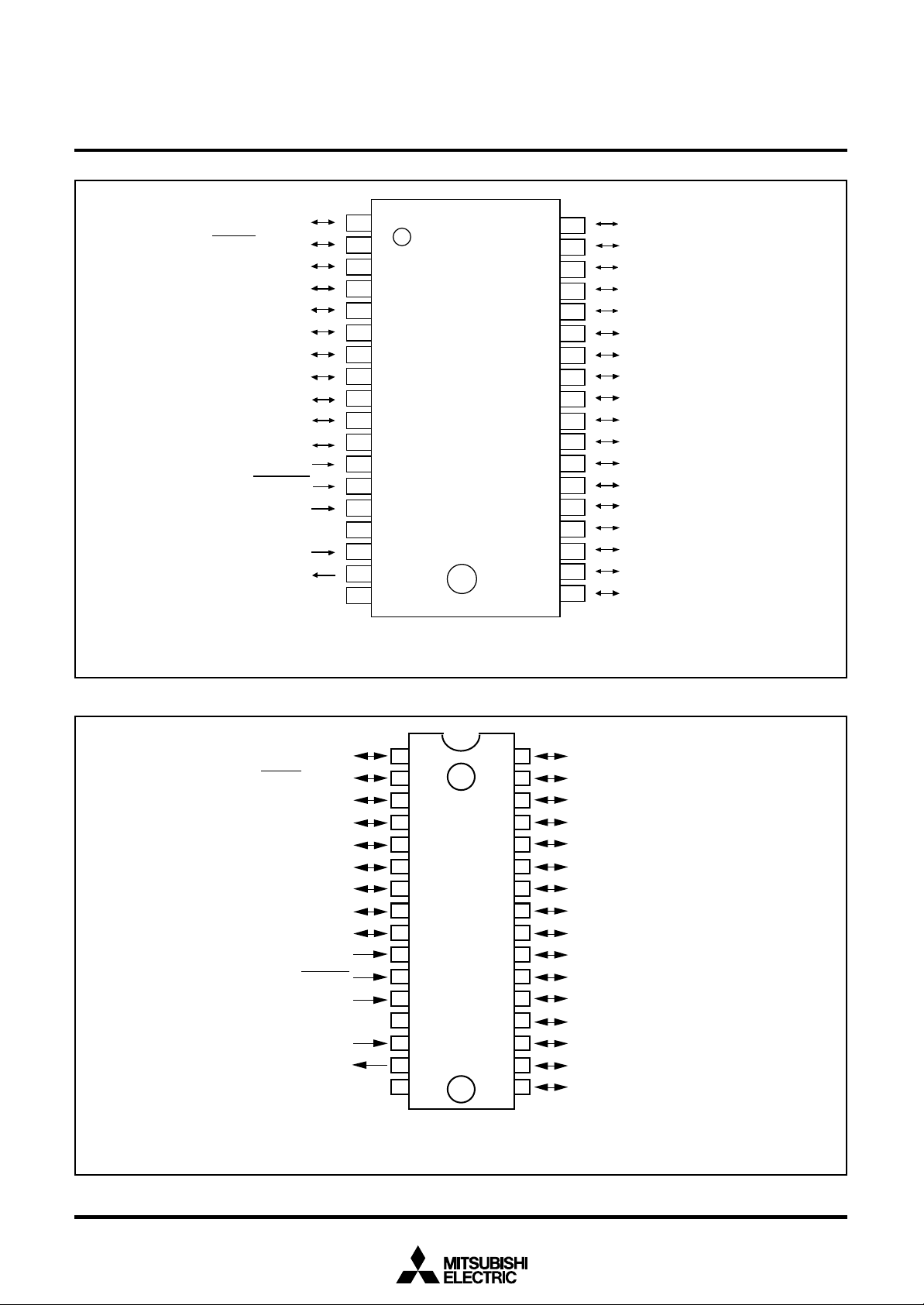
M37540M4-XXXFP
M37540E8FP
0
0
1
2
3
4
5
6
7
36
35
34
33
32
31
30
29
28
27
26
25
24
23
22
21
20
19
P11/TXD
P10/RXD
P0
P0
P0
P0
P03/TX
P02/TZ
P01/TY
1
1
7
6
5
4
OUT
OUT
OUT
P00/CNTR
P37/INT
P3
0
6
(LED6)/INT
P35(LED5)
P3
4
(LED4)
P3
3
(LED3)
P3
2
(LED2)
P31(LED1)
P30(LED0)
1
1
Package type: 36P2R-A
Fig. 2 M37540M4-XXXFP, M37540E8FP pin configuration
P12/S
CLK1/SCLK2
P13/S
RDY1/SDATA2
P14/CNTR
P20/AN
P21/AN
P22/AN
P23/AN
P24/AN
P25/AN
V
REF
RESET
CNV
SS
V
CC
X
X
OUT
V
SS
0
0
1
2
3
4
5
10
11
12
13
14
IN
14
15
15
16
16
Package type: 32P4B
1
2
3
4
5
6
7
8
9
M37540M4-XXXSP
M37540E8SP
32
31
30
29
28
27
26
25
24
23
22
21
20
19
18
17
P11/TXD
1
P10/RXD
P0
7
P0
6
P0
5
P0
4
P03/TX
P02/TZ
P01/TY
P0
P37/INT
0
/CNTR
OUT
OUT
OUT
0
P34(LED4)
P33(LED3)
P3
2
(LED2)
P3
1
(LED1)
P30(LED0)
1
1
Fig. 3 M37540M4-XXXSP, M37540E8SP pin configuration
2
Page 3
PRELIMINARY
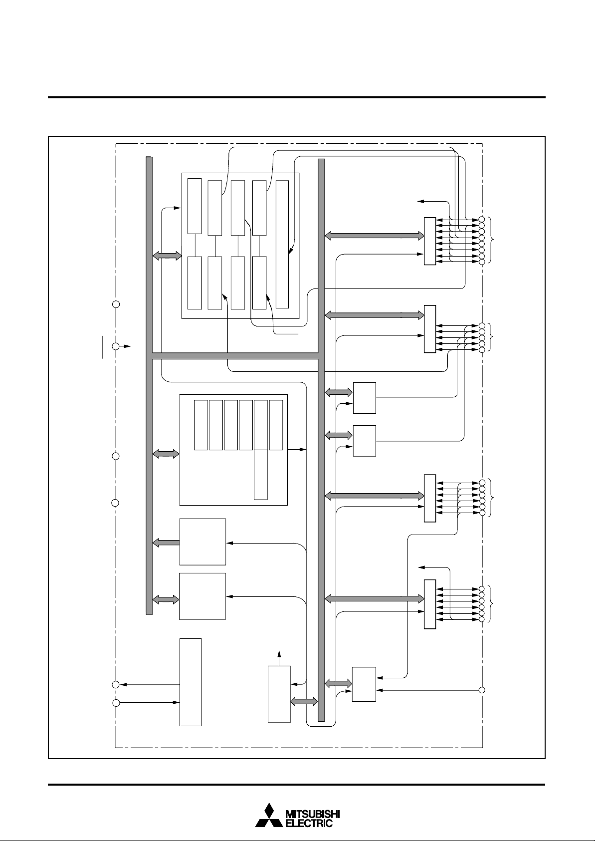
X
IN OUT
X
SI/O1(8)
RAM
ROM
CPU
A
X
Y
S
PC
H
PCLPS
V
SS
11
RESET
6
V
CC
8
7
CNV
SS
P1(5)
30 28 2629 27
32
31
P2(6)
P3(6)
1215 13
5
Reset input
I/O port P2
I/O port P1I/O port P3
Clock generating circuit
Clock input
Clock output
9
10
4
2
3
1
A-D
converter
(10)
V
REF
Watchdog timer
Reset
0
14
INT
0
1617
SI/O2(8)
CNTR
0
I/O port P0
Prescaler Y (8)
Prescaler Z (8)
Timer X (8)
Timer Z (8)
Timer Y (8)
Key-on wakeup
TY
OUT
TZ
OUT
Prescaler X (8)
CNTR
1
Timer A (16)
P0(8)
25
23 21
19
24 22
20 18
INT
0
Timer 1 (8)
Prescaler 1 (8)
TX
OUT
Notice: This is not a final specification.
Some parametric limits are subject to change.
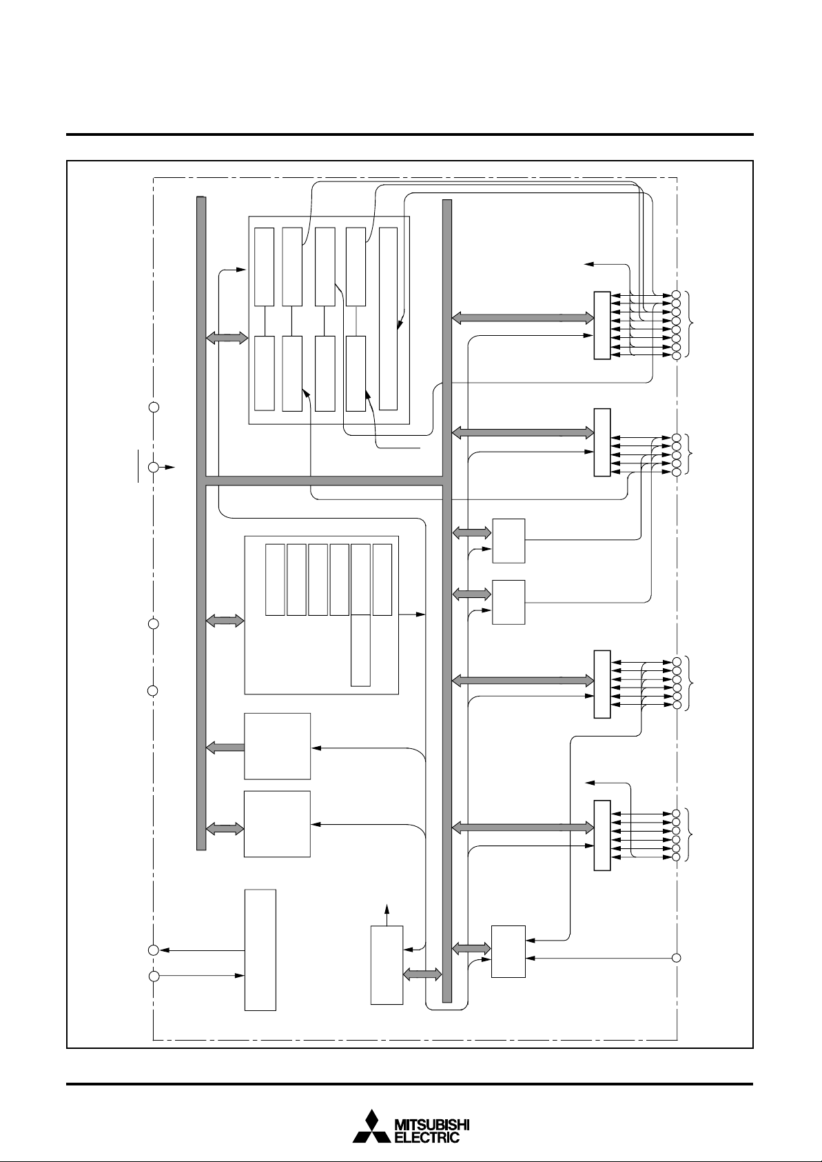
FUNCTIONAL BLOCK
MITSUBISHI MICROCOMPUTERS
7540 Group
SINGLE-CHIP 8-BIT CMOS MICROCOMPUTER
FUNCTIONAL BLOCK DIAGRAM (Package: 32P6B)
Fig. 4 Functional block diagram (32P6B package)
3
Page 4
PRELIMINARY
A-D
converter
(10)
X
IN OUT
X
CPU
V
SS
18
RESET
13
V
CC
15
14
CNV
SS
P0(8)
34
32 30 28
33
31 29 27
P1(5)
31
35
2
36
7
56
4
P2(8)
P3(8)
2023 21 19
12
I/O port P2
I/O port P0I/O port P1I/O port P3
16 17
11
9
10
8
0
22
26 2425
SI/O1(8)
RAM
ROM
A
X
Y
S
PC
H
PCL
PS
Reset input
Clock generating circuit
Clock input Clock output
V
REF
Watchdog timer
Reset
INT
0
SI/O2(8)
CNTR
0
Prescaler Y (8)
Prescaler Z (8)
Timer X (8)
Timer Z (8)
Timer Y (8)
Key-on wakeup
TY
OUT
TZ
OUT
Prescaler X (8)
CNTR
1
Timer A (16)
INT
0
Timer 1 (8)
Prescaler 1 (8)
TX
OUT
INT
1
Notice: This is not a final specification.
Some parametric limits are subject to change.
MITSUBISHI MICROCOMPUTERS
7540 Group
SINGLE-CHIP 8-BIT CMOS MICROCOMPUTER
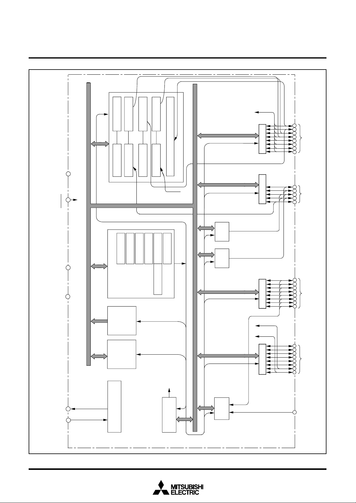
FUNCTIONAL BLOCK DIAGRAM (Package: 36P2R)
Fig. 5 Functional block diagram (36P2R package)
4
Page 5
PRELIMINARY
16
11
13
12
P1(5)
31
31
2
32
5
4
P2(6)
P3(6)
1720 18
10
14
15
9
7
8
6
0
19
2122
P0(8)
30
28 26 24
29
27 25 23
A-D
converter
(10)
X
IN OUT
X
CPU
V
SS
RESET
V
CC
CNV
SS
I/O port P2
I/O port P0I/O port P1
I/O port P3
SI/O1(8)
RAM
ROM
A
X
Y
S
PC
H
PC
L
PS
Reset input
Clock generating circuit
Clock input
Clock output
V
REF
Watchdog timer
Reset
INT
0
SI/O2(8)
CNTR
0
Prescaler Y (8)
Prescaler Z (8)
Timer X (8)
Timer Z (8)
Timer Y (8)
Key-on wakeup
TY
OUT
TZ
OUT
Prescaler X (8)
CNTR
1
Timer A (16)
INT
0
Timer 1 (8)
Prescaler 1 (8)
TX
OUT
Notice: This is not a final specification.
Some parametric limits are subject to change.
MITSUBISHI MICROCOMPUTERS
7540 Group
SINGLE-CHIP 8-BIT CMOS MICROCOMPUTER
FUNCTIONAL BLOCK DIAGRAM (Package: 32P4B)
Fig. 6 Functional block diagram (32P4B package)
5
Page 6
PRELIMINARY
Notice: This is not a final specification.
Some parametric limits are subject to change.
PIN DESCRIPTION
Table 1 Pin description
Pin
Vcc, Vss
VREF
CNVss
RESET
XIN
XOUT
P00/CNTR1
P01/TYOUT
P02/TZOUT
P03/TXOUT
P04–P07
P10/RxD1
P11/TxD1
P12/SCLK1/SCLK2
P13/SRDY1/SDATA2
P14/CNTR0
P20/AN0–
P27/AN7
P30–P35
P36/INT1
P37/INT0
Name
Power source
Analog reference
voltage
CNVss
Reset input
Clock input
Clock output
I/O port P0
I/O port P1
I/O port P2
I/O port P3
MITSUBISHI MICROCOMPUTERS
7540 Group
SINGLE-CHIP 8-BIT CMOS MICROCOMPUTER
Function
•Apply voltage of 2.2–5.5 V to Vcc, and 0 V to Vss.
•Reference voltage input pin for A-D converter
•Chip operating mode control pin, which is always connected to Vss.
•Reset input pin for active “L”
•Input and output pins for main clock generating circuit
•Connect a ceramic resonator or quartz crystal oscillator between the XIN and XOUT pins.
•For using RC oscillator, short between the XIN and XOUT pins, and connect the capacitor and resistor.
•If an external clock is used, connect the clock source to the XIN pin and leave the XOUT pin open.
•8-bit I/O port.
•I/O direction register allows each pin to be individually programmed as either input or output.
•CMOS compatible input level
•CMOS 3-state output structure
•Whether a built-in pull-up resistor is to be used or not can be
determined by program.
•5-bit I/O port
•I/O direction register allows each pin to be individually programmed as either input or output.
•CMOS compatible input level
•CMOS 3-state output structure
•CMOS/TTL level can be switched for P10, P12 and P13
•8-bit I/O port having almost the same function as P0
•CMOS compatible input level
•CMOS 3-state output structure
•8-bit I/O port
•I/O direction register allows each pin to be individually programmed as either input or output.
•CMOS compatible input level (CMOS/TTL level can be switched for P36 and P37).
•CMOS 3-state output structure
•P30 to P36 can output a large current for driving LED.
•Whether a built-in pull-up resistor is to be used or not can be
determined by program.
Function expect a port function
• Key-input (key-on wake up
interrupt input) pins
• Timer Y, timer Z, timer X and
timer A function pin
•Serial I/O1 function pin
•Serial I/O1 function pin
•Serial I/O2 function pin
•Timer X function pin
•Input pins for A-D converter
•Interrupt input pins
6
Page 7
PRELIMINARY
Notice: This is not a final specification.
Some parametric limits are subject to change.
MITSUBISHI MICROCOMPUTERS
7540 Group
SINGLE-CHIP 8-BIT CMOS MICROCOMPUTER
GROUP EXPANSION
Mitsubishi plans to expand the 7540 group as follow:
Memory type
Support for Mask ROM version, One Time PROM version, and Emulator MCU .
ROM size
(bytes)
32K
Under development
16K
Under development
Memory size
ROM/PROM size ................................................ 16 K to 32 K bytes
RAM size................................................................512 to 768 bytes
Package
32P4B ...........................................32-pin shrink plastic molded DIP
32P6B-A...................................... 0.8 mm-pitch plastic molded QFP
36P2R-A ..................................... 0.8 mm-pitch plastic molded SOP
42S1M.....................................42-pin shrink ceramic PIGGY BACK
Under development
M37540E8
M37540M4T
M37540M4
0
384
Note: Products under development•••the development schedule and
specification may be revised without notice.
Fig. 7 Memory expansion plan
Currently supported products are listed below.
Table 2 List of supported products
Product
M37540M4-XXXSP
M37540M4-XXXFP
M37540M4T-XXXFP
M37540M4-XXXGP
M37540M4T-XXXGP
M37540E8SP
M37540E8FP
M37540E8GP
M37540RSS
(P) ROM size (bytes)
ROM size for User ()
16384
(16254)
32768
(32638)
RAM size
(bytes)
512
768
768
Package
32P4B
36P2R-A
32P6B-A
32P4B
36P2R-A
32P6B-A
42S1M
512 768
Remarks
Mask ROM version
Mask ROM version
Mask ROM version (extended operating temperature version)
Mask ROM version
Mask ROM version (extended operating temperature version)
One Time PROM version (blank)
One Time PROM version (blank)
One Time PROM version (blank)
Emulator MCU
RAM size
(bytes)
7
Page 8
PRELIMINARY
Oscillation mode selection bit (Note 1)
0 : Ceramic oscillation
1 : RC oscillation
CPU mode register
(CPUM: address 003B
16
)
Stack page selection bit
0 : 0 page
1 : 1 page
Clock division ratio selection bits
b7 b6
0 0 : f(φ) = f(X
IN
)/2 (High-speed mode)
0 1 : f(φ) = f(X
IN
)/8 (Middle-speed mode)
1 0 : applied from ring oscillator
1 1 : f(φ) = f(X
IN
) (Double-speed mode)(Note 2)
Ring oscillator oscillation control bit
0 : Ring oscillator oscillation enabled
1 : Ring oscillator oscillation stop
X
IN
oscillation control bit
0 : Ceramic or RC oscillation enabled
1 : Ceramic or RC oscillation stop
Processor mode bits (Note 1)
b1 b0
0 0 Single-chip mode
0 1
1 0
1 1
Not available
b7 b0
2: These bits are used only when a ceramic oscillation is selected.
Note 1: The bit can be rewritten only once after releasing reset. After rewriting
it is disable to write any data to the bit. However, by reset the bit is
initialized and can be rewritten, again.
(It is not disable to write any data to the bit for emulator MCU
“M37540RSS”.)
Do not use these when an RC oscillation is selected.
Notice: This is not a final specification.
Some parametric limits are subject to change.
FUNCTIONAL DESCRIPTION
Central Processing Unit (CPU)
The 7540 Group uses the standard 740 family instruction set. Refer
to the table of 740 family addressing modes and machine-language
instructions or the 740 Family Software MANUAL for details on each
instruction set.
Machine-resident 740 family instructions are as follows:
1. The FST and SLW instructions cannot be used.
2. The MUL and DIV instructions can be used.
3. The WIT instruction can be used.
4. The STP instruction can be used.
(This instruction cannot be used while CPU operates by a ring oscillator.)
[CPU mode register] CPUM
The CPU mode register contains the stack page selection bit.
This register is allocated at address 003B16.
MITSUBISHI MICROCOMPUTERS
7540 Group
SINGLE-CHIP 8-BIT CMOS MICROCOMPUTER
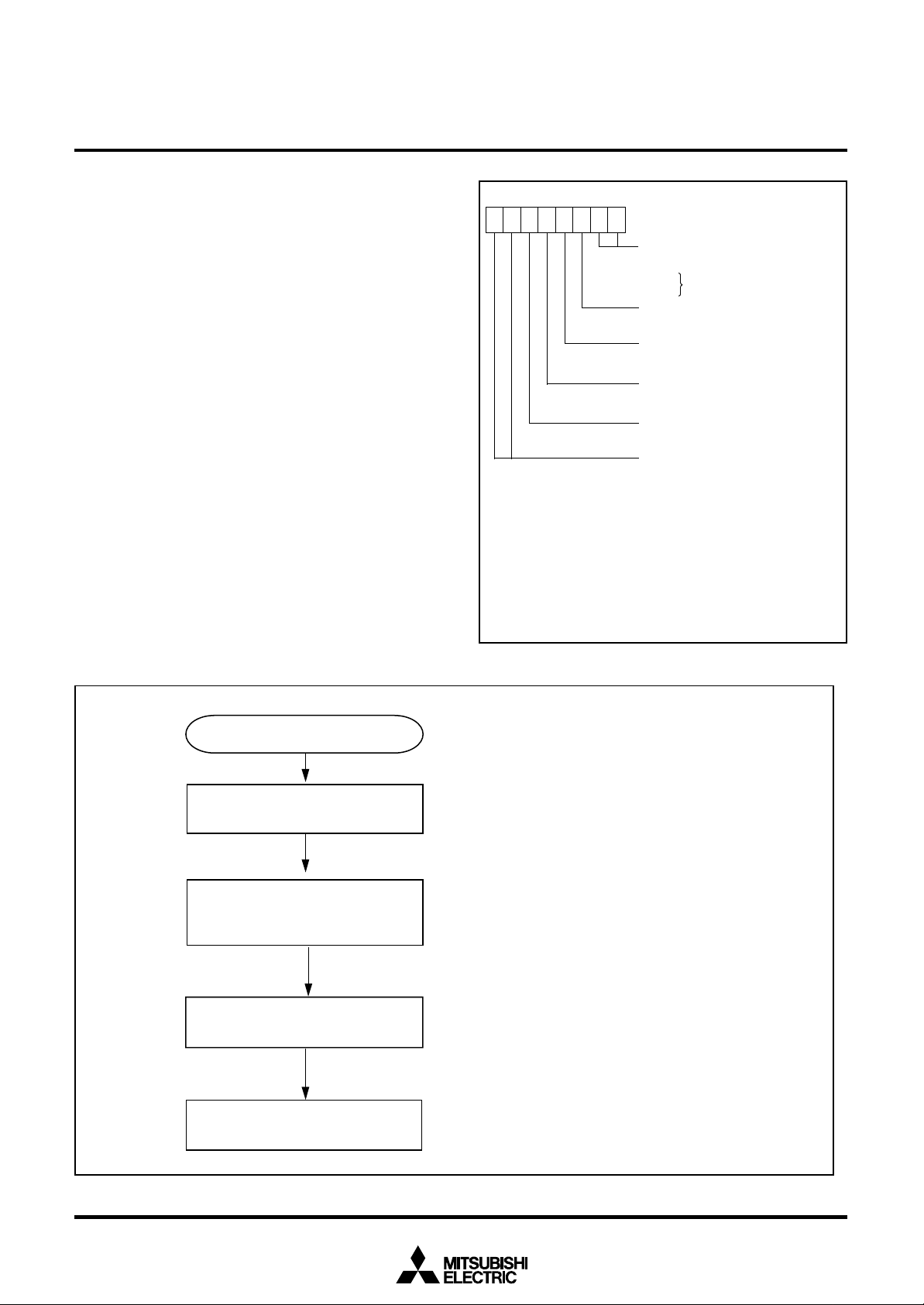
Switching method of CPU mode register
Switch the CPU mode register (CPUM) at the head of program after
releasing Reset in the following method.
After releasing reset
Switch the oscillation mode
selection bit (bit 5 of CPUM)
Fig. 9 Switching method of CPU mode register
8
Wait by ring oscillator operation until
establishment of oscillator clock
Switch the clock division ratio
selection bits (bits 6 and 7 of CPUM)
Main routine
Fig. 8 Structure of CPU mode register
Start with a built-in ring oscillator
An initial value is set as a ceramic
oscillation mode. When it is switched to an
RC oscillation, its oscillation starts.
When using a ceramic oscillation, wait until
establlishment of oscillation from oscillation starts.
When using an RC oscillation, wait time is not
required basically (time to execute the instruction to
switch from a ring oscillator meets the requirement).
Switch to other mode except a ring oscillator.
At the same time, select the double-speed,
high-speed, or middle-speed mode.
Page 9
PRELIMINARY
Notice: This is not a final specification.
Some parametric limits are subject to change.
MITSUBISHI MICROCOMPUTERS
7540 Group
SINGLE-CHIP 8-BIT CMOS MICROCOMPUTER
Memory
Special function register (SFR) area
The SFR area in the zero page contains control registers such as I/O
ports and timers.
RAM
RAM is used for data storage and for a stack area of subroutine calls
and interrupts.
ROM
The first 128 bytes and the last 2 bytes of ROM are reserved for
device testing and the rest is a user area for storing programs.
Interrupt vector area
The interrupt vector area contains reset and interrupt vectors.
RAM area
RAM capacity
(bytes)
512
768
address
XXXX16
023F16
033F16
Zero page
The 256 bytes from addresses 000016 to 00FF16 are called the zero
page area. The internal RAM and the special function registers (SFR)
are allocated to this area.
The zero page addressing mode can be used to specify memory and
register addresses in the zero page area. Access to this area with
only 2 bytes is possible in the zero page addressing mode.
Special page
The 256 bytes from addresses FF0016 to FFFF16 are called the special page area. The special page addressing mode can be used to
specify memory addresses in the special page area. Access to this
area with only 2 bytes is possible in the special page addressing
mode.
000016
SFR area
Zero page
RAM
004016
010016
XXXX
16
Reserved area
044016
Not used
ROM area
ROM capacity
(bytes)
16384
32768
Fig. 10 Memory map diagram
address
YYYY16
C00016
800016
address
ZZZZ16
C08016
808016
ROM
YYYY16
ZZZZ16
FF0016
FFDC16
FFFE16
FFFF16
Reserved ROM area
(128 bytes)
Interrupt vector area
Reserved ROM area
Special page
9
Page 10
PRELIMINARY
Notice: This is not a final specification.
Some parametric limits are subject to change.
MITSUBISHI MICROCOMPUTERS
7540 Group
SINGLE-CHIP 8-BIT CMOS MICROCOMPUTER
Port P0 (P0)
000016
Port P0 direction register (P0D)
000116
Port P1 (P1)
000216
Port P1 direction register (P1D)
000316
Port P2 (P2)
000416
Port P2 direction register (P2D)
000516
Port P3 (P3)
000616
Port P3 direction register (P3D)
000716
000816
000916
000A16
000B16
000C16
000D16
000E16
000F16
001016
001116
001216
001316
001416
001516
Pull-up control register (PULL)
001616
Port P1P3 control register (P1P3C)
001716
Transmit/Receive buffer register (TB/RB)
001816
Serial I/O1 status register (SIO1STS)
001916
Serial I/O1 control register (SIO1CON)
001A16
UART control register (UARTCON)
001B16
Baud rate generator (BRG)
001C16
Timer A mode register (TAM)
001D16
001E16
Timer A (low-order) (TAL)
001F16
Timer A (high-order) (TAH)
Timer Y, Z mode register (TYZM)
002016
Prescaler Y (PREY)
002116
Timer Y secondary (TYS)
002216
Timer Y primary (TYP)
002316
Timer Y, Z waveform output control register (PUM)
002416
Prescaler Z (PREZ)
002516
Timer Z secondary (TZS)
002616
Timer Z primary (TZP)
002716
Prescaler 1 (PRE1)
002816
Timer 1 (T1)
002916
One-shot start register (ONS)
002A16
Timer X mode register (TXM)
002B16
Prescaler X (PREX)
002C16
Timer X (TX)
002D16
Timer count source set register (TCSS)
002E16
002F16
Serial I/O2 control register (SIO2CON)
003016
Serial I/O2 register (SIO2)
003116
003216
003316
A-D control register (ADCON)
003416
A-D conversion register (low-order) (ADL)
003516
A-D conversion register (high-order) (ADH)
003616
003716
MISRG
003816
Watchdog timer control register (WDTCON)
003916
Interrupt edge selection register (INTEDGE)
003A16
CPU mode register (CPUM)
003B16
Interrupt request register 1 (IREQ1)
003C16
Interrupt request register 2 (IREQ2)
003D16
Interrupt control register 1 (ICON1)
003E16
Interrupt control register 2 (ICON2)
003F16
Note : Do not access to the SFR area including nothing.
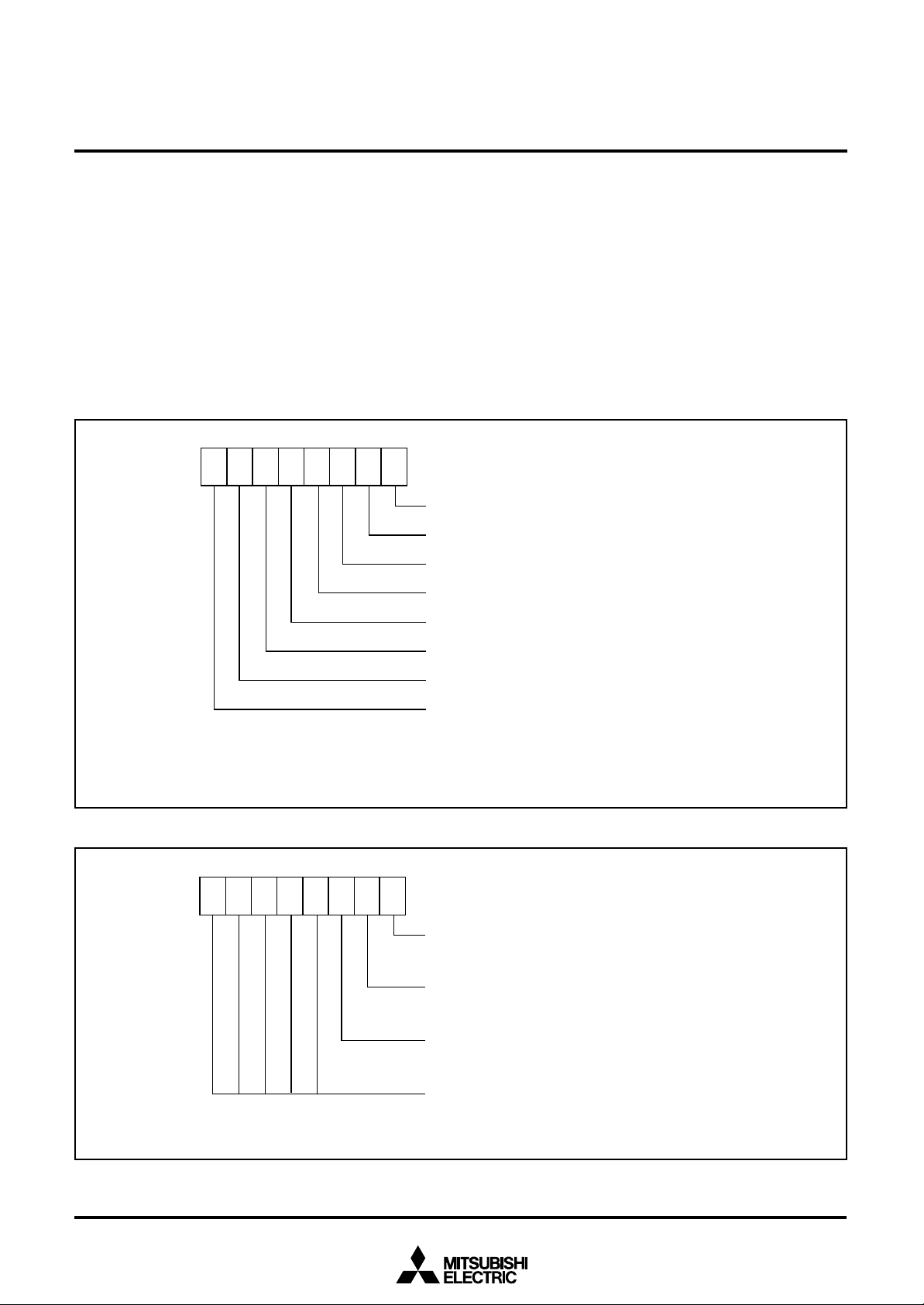
Fig. 11 Memory map of special function register (SFR)
10
Page 11
PRELIMINARY
Notice: This is not a final specification.
Some parametric limits are subject to change.
MITSUBISHI MICROCOMPUTERS
7540 Group
SINGLE-CHIP 8-BIT CMOS MICROCOMPUTER
I/O Ports
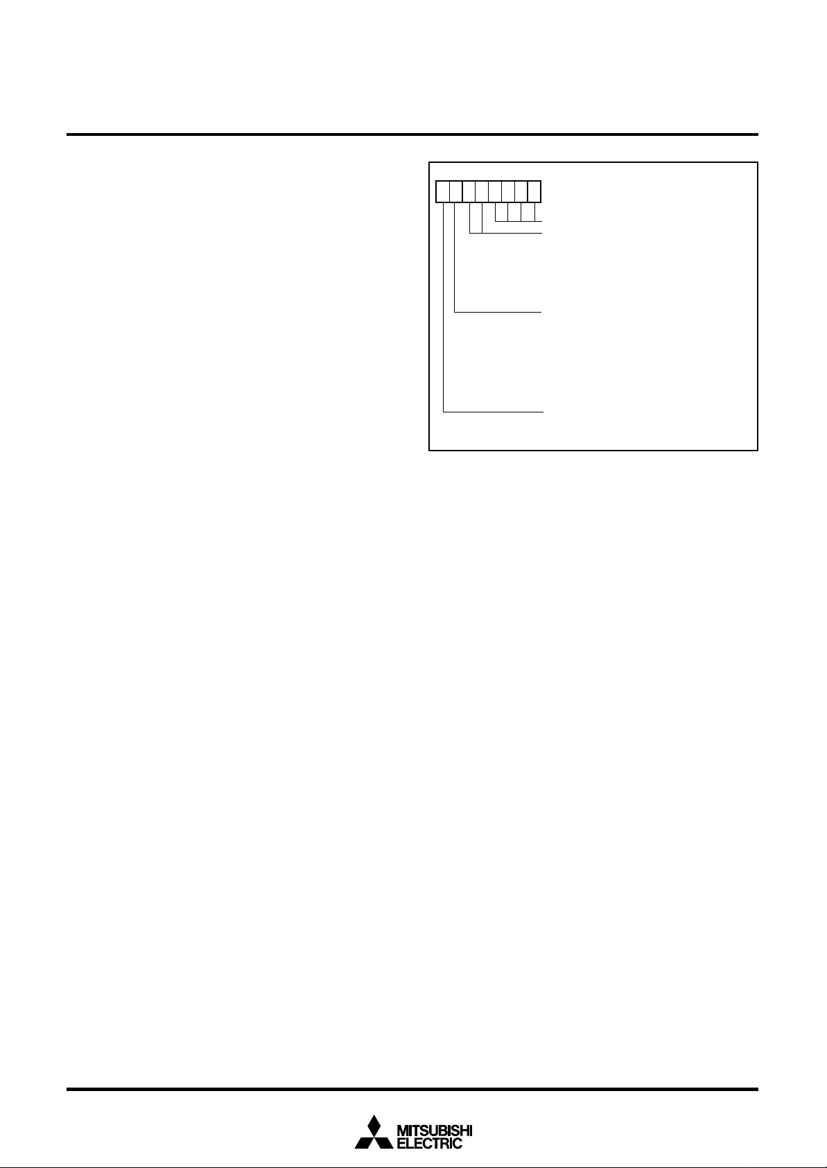
[Direction registers] PiD
The I/O ports have direction registers which determine the input/output direction of each pin. Each bit in a direction register corresponds
to one pin, and each pin can be set to be input or output.
When “1” is set to the bit corresponding to a pin, this pin becomes an
output port. When “0” is set to the bit, the pin becomes an input port.
When data is read from a pin set to output, not the value of the pin
itself but the value of port latch is read. Pins set to input are floating,
and permit reading pin values.
If a pin set to input is written to, only the port latch is written to and the
pin remains floating.
b7 b0
Pull-up control register
(PULL: address 0016
[Pull-up control register] PULL
By setting the pull-up control register (address 001616), ports P0 and
P3 can exert pull-up control by program. However, pins set to output
are disconnected from this control and cannot exert pull-up control.
[Port P1P3 control register] P1P3C
By setting the port P1P3 control register (address 001716), a CMOS
input level or a TTL input level can be selected for ports P10, P12,
P13, P36, and P37 by program.
16
, initial value: 0016)
P00 pull-up control bit
P0
1
pull-up control bit
P0
2
, P03 pull-up control bit
P0
4
– P07 pull-up control bit
P3
0
– P33 pull-up control bit
Note 1: Pins set to output ports are disconnected from pull-up control.
5
2: Set the P3
Fig. 12 Structure of pull-up control register
, P36 pull-up control bit to “1” (initial value: “0”) for 32-pin version.
b7 b0
Note: Keep setting the P36/INT1 input level selection bit
to “0” (initial value) for 32-pin version.
P3
4
pull-up control bit
P3
5
, P36 pull-up control bit
P3
7
pull-up control bit
Port P1P3 control register
(P1P3C: address 0017
P37/INT0 input level selection bit
0 : CMOS level
1 : TTL level
6
/INT1 input level selection bit
P3
0 : CMOS level
1 : TTL level
P1
0
,P12,P13 input level selection bit
0 : CMOS level
1 : TTL level
Not used
16
, initial value: 0016)
0 : Pull-up Off
1 : Pull-up On
Fig. 13 Structure of port P1P3 control register
11
Page 12
PRELIMINARY
Notice: This is not a final specification.
Some parametric limits are subject to change.
Table 3 I/O port function table
Pin
P00/CNTR1
P01/TYOUT
P02/TZOUT
P03/TXOUT
P04–P07
P10/RxD1
P11/TxD1
P12/SCLK1/SCLK2
P13/SRDY1/SDATA2
P14/CNTR0
P20/AN0–P27/AN7
P30–P35
P36/INT1
P37/INT0
Note: Ports P10, P12, P13, P36, and P37 are CMOS/TTL level.
Name
I/O port P0
I/O port P1
I/O port P2
I/O port P3
Input/output
I/O individual
bits
I/O format
•CMOS compatible input
level
•CMOS 3-state output
(Note)
MITSUBISHI MICROCOMPUTERS
7540 Group
SINGLE-CHIP 8-BIT CMOS MICROCOMPUTER
Non-port function
Key input interrupt
Serial I/O1 function
input/output
Serial I/O2 function
input/output
Timer X function
input/output
A-D conversion
input
External interrupt
input
Related SFRs Diagram No.
Pull-up control register
Timer Y mode register
Timer Z mode register
Timer X mode register
Timer Y,Z waveform output control register
Timer A mode register
Serial I/O1 control register
Serial I/O1 control register
Serial I/O2 control register
Timer X mode register
A-D control register
Interrupt edge selection
register
(1)
(2)
(3)
(4)
(5)
(6)
(7)
(8)
(9)
(10)
(11)
(12)
12
Page 13
PRELIMINARY
Notice: This is not a final specification.
Some parametric limits are subject to change.
MITSUBISHI MICROCOMPUTERS
7540 Group
SINGLE-CHIP 8-BIT CMOS MICROCOMPUTER
(1)Port P00
Data bus
(3)Port P03
Data bus
Pull-up control
Direction
register
Port latch
Direction
register
Port latch
Timer output
CNTR1 interrupt input
To key input interrupt
generating circuit
Pull-up control
P0
3
/TX
output valid
To key input interrupt
generating circuit
OUT
(2)Ports P01, P02
Pull-up control
Direction
register
Data bus Port latch
Pulse output mode
Timer output
To key input interrupt
generating circuit
(4)Ports P04–P07
Pull-up control
Direction
register
Data bus
Port latch
To key input interrupt
generating circuit
(5)Port P10
Serial I/O1 enable bit
Receive enable bit
Data bus
Direction
register
Port latch
Serial I/O1 input
(7)Port P12
CLK2
pin
S
Serial I/O1 synchronous
clock selection bit
Serial I/O1 enable bit
Serial I/O1 mode selection bit
Serial I/O1 enable bit
Data bus
Serial I/O1, serial I/O2 clock output
selection bit
Direction
register
Port latch
Serial I/O1, serial I/O2 clock input
P10, P12, P13, P36, and P37 input level are switched to the CMOS/TTL level by the port P1P3 control register.
*
Fig. 14 Block diagram of ports (1)
P1
0
, P12, P13
input level
selection bit
*
P1
0
, P12, P13
input level
selection bit
(6)Port P11
1/TxD1
P-channel output disable bit
P1
Serial I/O1 enable bit
Transmit enable bit
Direction
register
Data bus
Port latch
Serial I/O1 output
*
13
Page 14
PRELIMINARY
Notice: This is not a final specification.
Some parametric limits are subject to change.
MITSUBISHI MICROCOMPUTERS
7540 Group
SINGLE-CHIP 8-BIT CMOS MICROCOMPUTER
(8) Port P1
DATA2
S
Serial I/O mode selection bit
Data bus
3
output in operation signal
DATA2
pin selection bit
S
Serial I/O1 enable bit
S
RDY1
output enable bit
Serial I/O1 ready output
Serial I/O2 output
(10) Ports P20–P2
Data bus
Direction
register
Port latch
7
Direction
register
Port latch
Serial I/O2 input
P10, P12, P13
input level
selection bit
*
(9) Port P1
Data bus
4
Pulse output mode
(11) Ports P30–P3
Data bus
Direction
register
Port latch
Timer output
5
Pull-up control
Direction
register
Port latch
CNTR0 interrupt input
A-D converter input
(12) Ports P36, P3
Data bus
P10, P12, P13, P36, and P37 input level are switched to the CMOS/TTL level by the port P1P3 control register.
*
7
Pull-up control
Direction
register
Port latch
INT interrupt input
Fig. 15 Block diagram of ports (2)
Analog input pin
selection bit
P3 input level
selection bit
*
14
Page 15
PRELIMINARY
Notice: This is not a final specification.
Some parametric limits are subject to change.
MITSUBISHI MICROCOMPUTERS
7540 Group
SINGLE-CHIP 8-BIT CMOS MICROCOMPUTER
Interrupts
Interrupts occur by 15 different sources : 5 external sources, 9 internal sources and 1 software source.
Interrupt control
All interrupts except the BRK instruction interrupt have an interrupt
request bit and an interrupt enable bit, and they are controlled by the
interrupt disable flag. When the interrupt enable bit and the interrupt
request bit are set to “1” and the interrupt disable flag is set to “0”, an
interrupt is accepted.
The interrupt request bit can be cleared by program but not be set.
The interrupt enable bit can be set and cleared by program.
The reset and BRK instruction interrupt can never be disabled with
any flag or bit. All interrupts except these are disabled when the interrupt disable flag is set.
When several interrupts occur at the same time, the interrupts are
received according to priority.
Table 4 Interrupt vector address and priority
Vector addresses (Note 1)
Interrupt source
Reset (Note 2)
Serial I/O1 receive
Serial I/O1 transmit
INT0
INT1 (Note 3)
Key-on wake-up
CNTR0
CNTR1
Timer X
Timer Y
Timer Z
Timer A
Serial I/O2
A-D conversion
Timer 1
Reserved area
BRK instruction
Note 1: Vector addressed contain internal jump destination addresses.
2: Reset function in the same way as an interrupt with the highest priority.
3: It is an interrupt which can use only for 36 pin version.
Priority
1
2
3
4
5
6
7
8
9
10
11
12
13
14
15
16
17
High-order
FFFD16
FFFB16
FFF916
FFF716
FFF516
FFF316
FFF116
FFEF16
FFED16
FFEB16
FFE916
FFE716
FFE516
FFE316
FFE116
FFDF16
FFDD16
Low-order
FFFC16
FFFA16
FFF816
FFF616
FFF416
FFF216
FFF016
FFEE16
FFEC16
FFEA16
FFE816
FFE616
FFE416
FFE216
FFE016
FFDE16
FFDC16
Interrupt request generating conditions
At reset input
At completion of serial I/O1 data receive
At completion of serial I/O1 transmit shift or
when transmit buffer is empty
At detection of either rising or falling edge of
INT0 input
At detection of either rising or falling edge of
INT1 input
At falling of conjunction of input logical level for
port P0 (at input)
At detection of either rising or falling edge of
CNTR0 input
At detection of either rising or falling edge of
CNTR1 input
At timer X underflow
At timer Y underflow
At timer Z underflow
At timer A underflow
At completion of transmit/receive shift
At completion of A-D conversion
At timer 1 underflow
Not available
At BRK instruction execution
Interrupt operation
Upon acceptance of an interrupt the following operations are automatically performed:
1. The processing being executed is stopped.
2. The contents of the program counter and processor status register are automatically pushed onto the stack.
3. The interrupt disable flag is set and the corresponding interrupt
request bit is cleared.
4. Concurrently with the push operation, the interrupt destination
address is read from the vector table into the program counter.
Notes on use
When the active edge of an external interrupt (INT0, INT1,CNTR0) is
set, the interrupt request bit may be set.
Therefore, please take following sequence:
1. Disable the external interrupt which is selected.
2. Change the active edge in interrupt edge selection register. (in
case of CNTR0: Timer X mode register, in case of CNTR1: Timer
A mode register)
3. Clear the set interrupt request bit to “0”.
4. Enable the external interrupt which is selected.
Remarks
Non-maskable
Valid only when serial I/O1 is selected
Valid only when serial I/O1 is selected
External interrupt
(active edge selectable)
External interrupt
(active edge selectable)
External interrupt (valid at falling)
External interrupt
(active edge selectable)
External interrupt
(active edge selectable)
STP release timer underflow
Non-maskable software interrupt
15
Page 16
PRELIMINARY
Notice: This is not a final specification.
Some parametric limits are subject to change.
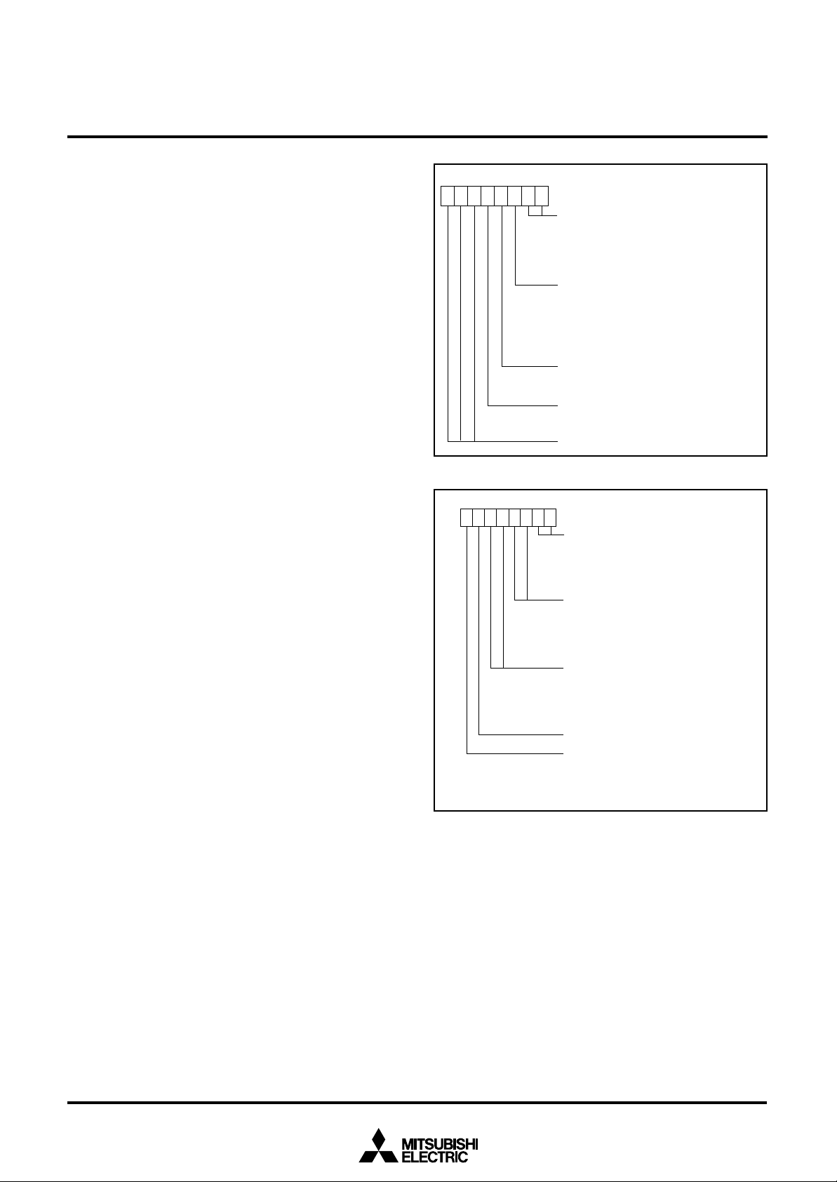
Interrupt request bit
Interrupt enable bit
Interrupt disable flag I
MITSUBISHI MICROCOMPUTERS
7540 Group
SINGLE-CHIP 8-BIT CMOS MICROCOMPUTER
Fig. 16 Interrupt control
b7 b0
b7 b0
b7 b0
BRK instruction
Reset
Interrupt edge selection register
(INTEDGE : address 003A
INT0 interrupt edge selection bit
0 : Falling edge active
1 : Rising edge active
INT
1
interrupt edge selection bit
0 : Falling edge active
1 : Rising edge active
Not used (returns “0” when read)
P0
0
key-on wakeup enable bit
0 : Key-on wakeup enabled
1 : Key-on wakeup disabled
Interrupt request register 1
(IREQ1 : address 003C
Serial I/O1 receive interrupt request bit
Serial I/O1 transmit interrupt request bit
INT0 interrupt request bit
INT
1
interrupt request bit
Key-on wake up interrupt request bit
CNTR
0
interrupt request bit
CNTR
1
interrupt request bit
Timer X interrupt request bit
Interrupt request register 2
(IREQ2 : address 003D
Timer Y interrupt request bit
Timer Z interrupt request bit
Timer A interrupt request bit
Serial I/O2 interrupt request bit
A-D conversion interrupt request bit
Timer 1 interrupt request bit
Not used (returns “0” when read)
16
)
16
)
16
)
Interrupt request
0 : No interrupt request issued
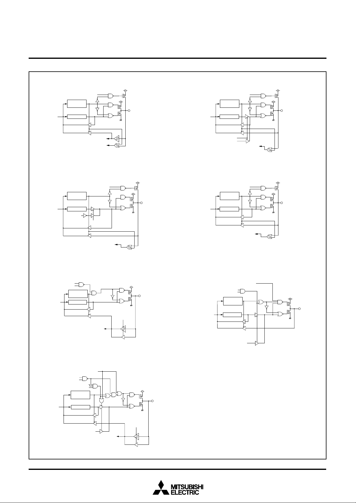
1 : Interrupt request issued
0 : No interrupt request issued
1 : Interrupt request issued
b7 b0
b7 b0
Interrupt control register 1
(ICON1 : address 003E
Serial I/O1 receive interrupt enable bit
Serial I/O1 transmit interrupt enable bit
INT
0
interrupt enable bit
INT
1
interrupt enable bit
Key-on wake up interrupt enable bit
CNTR
0
CNTR
1
Timer X interrupt enable bit
Interrupt control register 2
(ICON2 : address 003F
Timer Y interrupt enable bit
Timer Z interrupt enable bit
Timer A interrupt enable bit
Serial I/O2 interrupt enable bit
A-D conversion interrupt enable bit
Timer 1 interrupt enable bit
Not used (returns “0” when read)
(Do not write “1” to this bit)
Fig. 17 Structure of Interrupt-related registers
16
16
)
interrupt enable bit
interrupt enable bit
16
)
0 : Interrupts disabled
1 : Interrupts enabled
0 : Interrupts disabled
1 : Interrupts enabled
Page 17
PRELIMINARY
Notice: This is not a final specification.
Some parametric limits are subject to change.
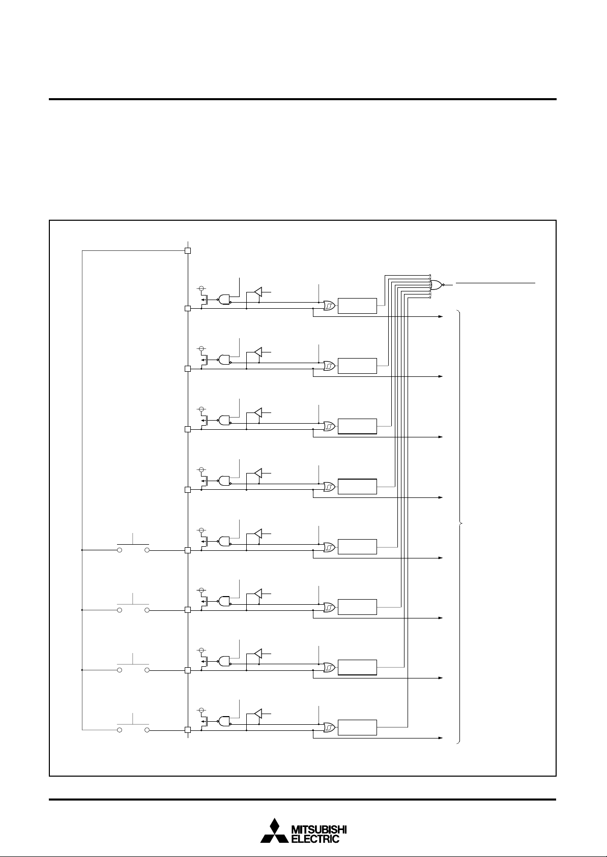
Key Input Interrupt (Key-On Wake-Up)
A key-on wake-up interrupt request is generated by applying “L” level
to any pin of port P0 that has been set to input mode.
In other words, it is generated when the AND of input level goes from
“1” to “0”. An example of using a key input interrupt is shown in Figure 18, where an interrupt request is generated by pressing one of
the keys provided as an active-low key matrix which uses ports P00
to P03 as input ports.
Port PXx
“L” level output
PULL register
bit 3 = “0”
***
Port P0
P07 output
latch
7
Port P0
Direction register = “1”
7
Falling edge
detection
MITSUBISHI MICROCOMPUTERS
7540 Group
SINGLE-CHIP 8-BIT CMOS MICROCOMPUTER
Key input interrupt request
P0
P0
P0
P0
P0
P0
P0
6
output
5
output
4
output
3
2
1
0
input
input
input
input
PULL register
bit 3 = “0”
***
PULL register
bit 3 = “0”
***
PULL register
bit 3 = “0”
***
PULL register
bit 2 = “1”
***
PULL register
bit 2 = “1”
***
PULL register
bit 1 = “1”
***
PULL register
bit 0 = “1”
***
Port P0
Direction register = “1”
Port P0
6
latch
Port P0
Direction register = “1”
Port P0
5
latch
Port P0
Direction register = “1”
Port P0
4
latch
Port P0
Direction register = “0”
Port P0
3
latch
Port P0
Direction register = “0”
Port P0
2
latch
Port P0
Direction register = “0”
Port P0
1
latch
Port P0
Direction register = “0”
Port P0
0
latch
6
5
4
3
2
1
0
Falling edge
detection
Falling edge
detection
Falling edge
detection
Falling edge
detection
Falling edge
detection
Falling edge
detection
Falling edge
detection
Port P0
Input read circuit
* P-channel transistor for pull-up
** CMOS output buffer
Fig. 18 Connection example when using key input interrupt and port P0 block diagram
17
Page 18
PRELIMINARY
Notice: This is not a final specification.
Some parametric limits are subject to change.
MITSUBISHI MICROCOMPUTERS
7540 Group
SINGLE-CHIP 8-BIT CMOS MICROCOMPUTER
Timers
The 7540 Group has 5 timers: timer 1, timer A, timer X, timer Y and
timer Z.
The division ratio of every timer and prescaler is 1/(n+1) provided
that the value of the timer latch or prescaler is n.
All the timers are down count timers. When a timer reaches “0”, an
underflow occurs at the next count pulse, and the corresponding timer
latch is reloaded into the timer. When a timer underflows, the interrupt request bit corresponding to each timer is set to “1”.
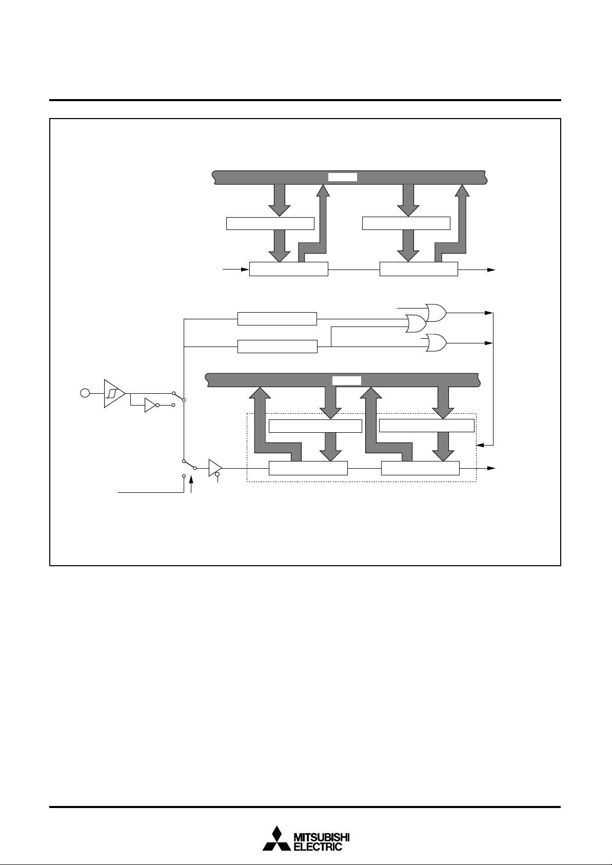
●Timer 1
Prescaler 1 always counts f(XIN)/16. Timer 1 always counts the
prescaler 1 output and periodically sets the interrupt request bit.
●Timer A
Timer A is a 16-bit timer that can be selected in one of four modes.
• Timer Mode
The timer counts f(XIN)/16.
• Period Measurement Mode
CNTR1 interrupt request is generated at rising/falling edge of
CNTR1 pin input signal. Simultaneously, the value in timer A latch
is reloaded in timer A and timer A continues counting down. Except for the above-mentioned, the operation in period measurement mode is the same as in timer mode.
The timer value just before the reloading at rising/falling of CNTR1
pin input signal is retained until the timer A is read once after the
reload.
The rising/falling timing of CNTR1 pin input signal is found by CNTR1
interrupt.
b7 b0
Timer A mode register
(TAM : address 001D
Not used (return “0” when read)
Timer A operating mode bits
b5 b4
0 0 : Timer mode
0 1 : Period measurement mode
1 0 : Event counter mode
1 1 : Pulse width HL continuously
measurement mode
CNTR
1
active edge switch bit
0 : Count at rising edge in event counter mode
Measure the falling edge period in period
measurement mode
Falling edge active for CNTR
1 : Count at falling edge in event counter mode
Measure the rising edge period in period
measurement mode
Rising edge active for CNTR
Timer A stop control bit
0 : Count start
1 : Count stop
Fig. 19 Structure of timer A mode register
16
)
1
interrupt
1
interrupt
• Event Counter Mode
The timer counts signals input through the CNTR1 pin.
Except for this, the operation in event counter mode is the same
as in timer mode.
• Pulse Width HL Continuously Measure-ment Mode
CNTR1 interrupt request is generated at both rising and falling
edges of CNTR1 pin input signal. Except for this, the operation in
pulse width HL continuously measurement mode is the same as in
period measurement mode.
■ Note
● CNTR1 interrupt active edge selection
CNTR1 interrupt active edge depends on the CNTR1 active edge
switch bit. However, in pulse width HL continuously measurement
mode, CNTR1 interrupt request is generated at both rising and
falling edges of CNTR1 pin input signal regardless of the setting of
CNTR1 active edge switch bit.
18
Page 19
PRELIMINARY
Notice: This is not a final specification.
Some parametric limits are subject to change.
MITSUBISHI MICROCOMPUTERS
7540 Group
SINGLE-CHIP 8-BIT CMOS MICROCOMPUTER
●Timer X
Timer X can be selected in one of 4 operating modes by setting the
timer X mode register.
• Timer Mode
The timer counts the signal selected by the timer X count source
selection bits.
• Pulse Output Mode
The timer counts the signal selected by the timer X count source
selection bits, and outputs a signal whose polarity is inverted each
time the timer value reaches “0”, from the CNTR0 pin.
When the CNTR0 active edge switch bit is “0”, the output of the
CNTR0 pin is started with an “H” output. At “1”, this output is started
with an “L” output. When using a timer in this mode, set the port
P14 direction register to output mode. Also, in the pulse output
mode, the inverted waveform of pulse output from CNTR0 pin can
be output from TXOUT pin by setting the P03/TXOUT output valid
bit to “1” . When using a timer in this mode, set the port P03 direction register to output mode.
• Event Counter Mode
The operation in the event counter mode is the same as that in
the timer mode except that the timer counts the input signal from
the CNTR0 pin.
When the CNTR0 active edge switch bit is “0”, the timer counts
the rising edge of the CNTR0 pin. When this bit is “1”, the timer
counts the falling edge of the CNTR0 pin.
• Pulse Width Measurement Mode
When the CNTR0 active edge switch bit is “0”, the timer counts
the signal selected by the timer X count source selection bit while
the CNTR0 pin is “H”. When this bit is “1”, the timer counts the
signal while the CNTR0 pin is “L”.
In any mode, the timer count can be stopped by setting the timer
X count stop bit to “1”. Each time the timer overflows, the interrupt
request bit is set.
b7 b0
Timer X mode register
(TXM : address 002B
Timer X operating mode bits
b1 b0
0 0 : Timer mode
0 1 : Pulse output mode
1 0 : Event counter mode
1 1 : Pulse width measurement mode
CNTR
0
active edge switch bit
0 : Interrupt at falling edge
Count at rising edge
(in event counter mode)
1 : Interrupt at rising edge
Count at falling edge
(in event counter mode)
Timer X count stop bit
0 : Count start
1 : Count stop
P03/TX
OUT
0 : Output invalid (I/O port)
1 : Output valid (Inverted CNTR
Not used (return “0” when read)
output valid bit
Fig. 20 Structure of timer X mode register
b7 b0
Timer count source set register
(TCSS : address 002E
Timer X count source selection bits
b1 b0
0 0 : f(X
0 1 : f(X
1 0 : f(X
1 1 : Not available
Timer Y count source selection bits
b3 b2
0 0 : f(X
0 1 : f(X
1 0 : Ring oscillator output (Note)
1 1 : Not available
Timer Z count source selection bits
b5 b4
0 0 : f(X
0 1 : f(X
1 0 : Timer Y underflow
1 1 : Not available
Fix this bit to “0”.
Not used (return “0” when read)
IN)/16
IN)/2
IN)
IN)/16
IN)/2
IN)/16
IN)/2
16
16)
)
0
output)
Note : System operates using a ring oscillator as a count source by setting
the ring oscillator to oscillation enabled by bit 3 of CPUM.
Fig. 21 Timer count source set register
19
Page 20

PRELIMINARY
Notice: This is not a final specification.
Some parametric limits are subject to change.
MITSUBISHI MICROCOMPUTERS
7540 Group
SINGLE-CHIP 8-BIT CMOS MICROCOMPUTER
●Timer Y
Timer Y is an 8-bit timer and can be selected in one of 2 operating
modes by setting the timer Y, Z mode register (TYZM).
• Timer mode
• Programmable waveform generation mode
The division ratio of timer Y and prescaler Y is 1/(n+1) provided that
the value of the timer latch or prescaler Y latch is n.
(1)Timer mode
• Mode select
Timer mode is selected by setting timer Y operation mode bit (b0)
of TYZM to “0”.
• Count source select
The count source is f(XIN)/2 or f(XIN)/16.
• Interrupt
When an underflow occurs, timer Y interrupt request bit (b0) of
IREQ2 is set to “1”.
• Operation description
After reset release, timer Y is operating because the timer Y count
stop bit (b3) of TYZM is “0”. Timer operation is stopped by setting
b3 of TYZM to “1”. In the timer mode, the timer count value is set
by timer Y primary latch (TYP). When a value is set to TYP while
timer is stopped, the setting value is written to latch and timer simultaneously.
When timer Y reaches “00”, an underflow occurs at the next count
pulse, and the timer Y latch is reloaded into the timer and count
continues. When timer value is changed during the count operation, either “writing to latch and timer simultaneously” or “writing to
only latch” can be selected by setting the timer Y write control bit
(b2) of TYZM. When selecting “writing to only latch”, the timer count
value is changed after the next underflow.
(2)Programmable waveform generation mode
• Mode select
Timer mode is selected by setting timer Y operation mode bit (b0)
of TYZM to “1”.
When this mode is selected, set timer Y write control bit (b2) of
TYZM to “1” (“writing to only latch” selected).
• Count source select
The count source is f(XIN)/2 or f(XIN)/16.
• Interrupt
When an underflow occurs, timer Y interrupt request bit (b0) of
IREQ is set to “1”.
• Operation description
After reset release, timer Y is operating because the timer Y count
stop bit (b3) of TYZM is “0”. MCU operates in the programmable
waveform generation mode when timer Y operation mode bit (b0)
of TYZM is set to “1” and b3 to “0” after timer Y operation is stopped
by setting b3 of TYZM to “1”.
In the programmable waveform generation mode, timer counts the
setting value of timer Y primary latch (TYP) and the setting value
of timer Y secondary latch (TYS) alternately, the waveform inverted
each time TYP and TYS underflow is output from TYOUT pin. The
active edge of output waveform is set by the timer Y output level
latch (b4) of the timer Y, Z waveform output control register (PUM).
When “0” is set to b4 of PUM, the initial state of timer at stop is “L”,
and “H” interval by the setting value of TYP or “L” interval by the
setting value of TYS is output alternately. When “1” is set to b4 of
PUM, the initial state of timer at stop is “H”, and “L” interval by the
setting value of TYP or “H” interval by the setting value of TYS is
output alternately.
Also, in this mode, the primary interval and the secondary interval
of the output waveform can be extended respectively for 0.5 cycle
of timer count source clock by setting the timer Y primary waveform extension control bit (b0) and the timer Y secondary waveform extension control bit (b1) of PUM to “1”. As a result, the waveforms of more accurate resolution can be output.
When b0 and b1 of PUM are used, the frequency and duty of the
output waveform are as follows;
Waveform frequency:
FTYOUT = (2 ✕ TMCL)/(2 ✕ (TYP+1) + 2 ✕ (TYS) + (EXPYP + EXPYS))
Duty:
DTYOUT = (2 ✕ (TYP + 1)) + EXPYP)/(2 ✕ (TYS + 1) + EXPYS))
TMCL: Timer Y count clock f(XIN)/2 or f(XIN)/16
TYP: Timer Y primary latch (8 bits)
TYS: Timer Y secondary latch (8 bits)
EXPYP: Timer Y primary waveform extension control bit (1 bit)
EXPYS: Timer Y secondary waveform extension control bit (1 bit)
When using the programmable waveform generation mode, note
the following;
Notes on using the programmable waveform generation mode
• When setting and changing TYP, TYS, EXPYP and EXPYS, write
to TYP at last because the setting to them is executed all at once
by writing to TYP. Even when TYP is not changed, write the same
value. The value is reloaded to timer at the beginning of the next
primary interval.
• Set by software in order not to execute the writing to timer Y primary and the timing of timer underflow simultaneously. When reading the timer Y secondary, the undefined value is read out. However, while timer counts the setting value of the timer Y secondary,
the count values at the secondary interval can be identified by
reading the timer Y primary.
• In this mode, set port P01 which is also used as TYOUT pin to output.
• B0 and b1 of PUM can be used only when “0016” is set to prescaler
Y.
20
Page 21

PRELIMINARY
Notice: This is not a final specification.
Some parametric limits are subject to change.
MITSUBISHI MICROCOMPUTERS
7540 Group
SINGLE-CHIP 8-BIT CMOS MICROCOMPUTER
●Timer Z
Timer Z is an 8-bit timer and can be selected in one of 4 operating
modes by setting the timer YZ mode register (TYZM).
• Timer mode
• Programmable waveform generation mode
• Programmable one-shot generation mode
• Programmable wait one-shot generation mode
The division ratio of timer Z and prescaler Z is 1/(n+1) provided that
the value of the timer Z latch or prescaler Z latch is n.
(1)Timer mode
• Mode select
Timer mode is selected by setting timer Z operation mode bits
(b5,b4) of TYZM to “00”.
• Count source select
The count source is f(XIN)/2, f(XIN)/16 or timer Y underflow.
• Interrupt
When an underflow occurs, timer Z interrupt request bit (b1) of
IREQ2 is set to “1”.
• Operation description
After reset release, timer Z is operating because the timer Z count
stop bit (b7) is “0”. Timer operation is stopped by setting b7 of
TYZM to “1”. In the timer mode, the timer count value is set by
timer Z primary latch (TZP). When a value is set to TZP while timer
is stopped, the setting value is written to latch and timer simultaneously.
When timer Z reaches “00”, an underflow occurs at the next count
pulse, and the timer Z latch is reloaded into the timer and count
continues. When timer value is changed during the count operation, either “writing to latch and timer simultaneously” or “writing to
only latch” can be selected by setting the timer Z write control bit
(b6) of TYZM. When selecting “writing to only latch”, the timer count
value is changed after the next underflow.
In the programmable waveform generation mode, timer counts the
setting value of timer Z primary latch (TZP) and the setting value
of timer Z secondary latch (TZS) alternately, the waveform inverted
each time TZP and TZS underflow is output from TZOUT pin. The
active edge of output waveform is set by the timer Z output level
latch (b5) of the timer Y, Z waveform output control register (PUM).
When “0” is set to b5 of PUM, the initial state of timer at stop is “L”,
and “H” interval by the setting value of TZP or “L” interval by the
setting value of TZS is output alternately. When “1” is set to b5 of
PUM, the initial state of timer at stop is “H”, and “L” interval by the
setting value of TZP or “H” interval by the setting value of TZS is
output alternately.
Also, in this mode, the primary interval and the secondary interval
of the output waveform can be extended respectively for 0.5 cycle
of timer count source clock by setting the timer Z primary waveform extension control bit (b2) and the timer Z secondary waveform extension control bit (b3) of PUM to “1”. As a result, the waveforms of more accurate resolution can be output.
When b2 and b3 of PUM are used, the frequency and duty of the
output waveform are as follows;
Waveform frequency:
FTZOUT = (2 ✕ TMCL)/(2 ✕ (TZP + 1)+2 ✕ (TZS) + (EXPZP + EXPZS))
Duty:
DTZOUT = (2 ✕ (TZP + 1)) + EXPZP)/(2 ✕ (TZS+1) + EXPZS))
TMCL: Timer Z count clock f(XIN)/2 or f(XIN)/16
TZP: Timer Z primary latch (8 bits)
TZS: Timer Z secondary latch (8 bits)
EXPZP: Timer Z primary waveform extension control bit (1 bit)
EXPZS: Timer Z secondary waveform extension control bit (1 bit)
When using the programmable waveform generation mode, note
the following;
(2)Programmable waveform generation mode
• Mode select
Timer mode is selected by setting timer Z operation mode bits
(b5,b4) of TYZM to “01”.
When this mode is selected, set timer Z write control bit (b6) of
TYZM to “1” (“writing to only latch” selected).
• Count source select
The count source is f(XIN)/2, f(XIN)/16 or timer Y underflow.
• Interrupt
When an underflow occurs, timer Z interrupt request bit (b1) of
IREQ is set to “1”.
• Operation description
After reset release, timer Z is operating because the timer Z count
stop bit (b7) of TYZM is “0”. MCU operates in the programmable
waveform generation mode when timer Z operation mode bits (b5,
b4) of TYZM is set to “01” and b7 to “0” after timer Z operation is
stopped by setting b7 of TYZM to “1”.
Notes on using the programmable waveform generation mode
• When setting and changing TZP, TZS, EXPZP and EXPZS, write
to TZP at last because the setting to them is executed all at once
by writing to TZP. Even when TZP is not changed, write the same
value. The value is reloaded to timer at the beginning of the next
primary interval.
• Set by software in order not to execute the writing to timer Z primary and the timing of timer underflow simultaneously. When reading the timer Z secondary, the undefined value is read out. However, while timer counts the setting value of the timer Z secondary,
the count values at the secondary interval can be identified by
reading the timer Z primary.
• In this mode, set port P02 which is also used as TZOUT pin to output.
• B2 and b3 of PUM can be used only when “0016” is set to prescaler
Z and f(XIN)/2 or f(XIN)/16 is selected as the timer Z count source.
21
Page 22

PRELIMINARY
Notice: This is not a final specification.
Some parametric limits are subject to change.
MITSUBISHI MICROCOMPUTERS
7540 Group
SINGLE-CHIP 8-BIT CMOS MICROCOMPUTER
(3)Programmable one-shot generation mode
• Mode select
Timer mode is selected by setting timer Z operation mode bits
(b5,b4) of TYZM to “10”.
When this mode is selected, set timer Z write control bit (b6) of
TYZM to “1” (“writing to only latch” selected).
• Count source select
The count source is f(XIN)/2, f(XIN)/16 or timer Y underflow.
• Interrupt
When an underflow occurs, timer Z interrupt request bit (b1) of
IREQ2 is set to “1”.
• Operation description
After reset release, timer Z is operating because the timer Z count
stop bit (b7) of TYZM is “0”. MCU operates in the programmable
one-shot generation mode when timer Z operation mode bits (b5,
b4) of TYZM is set to “10” after timer Z operation is stopped by
setting b7 of TYZM to “1”.
Timer Z is enabled to accept the one-shot start trigger when “0” is
written to b7 of TYZM after the timer count value is set to the timer
Z primary latch (TZP). In this state, when “1” is written to the timer
Z one-shot start bit (b0) of the one-shot start register (ONS), timer
Z starts count operation, at the same time, the output of TZOUT pin
is inverted. Timer Z counts down the value of TZP and stops after
the output of TZOUT pin is inverted to the same level as the initial
state when an underflow occurs. In this time, the next one-shot
pulse can be output by writing b0 of ONS to “1” because this bit is
initialized to “0”.
The active edge of the output waveform from TZOUT pin is set by
the timer Z output level latch (b5) of PUM. When “0” is set to b5 of
PUM, the initial level of timer at stop is “L” and “H” is output at the
same time when timer starts. “H” is output in the count interval of
TZP, and the output is inverted to “L” and stopped when an underflow occurs.
Also, when “1” is set to b5 of PUM, the initial level of timer at stop
is “H” and “L” is output at the same time when timer starts. “L” is
output in the count interval of TZP, and the output is inverted to “H”
and stopped when an underflow occurs.
When the INT0 pin one-shot trigger control bit (b6) of PUM is set
to “1”, the one-shot pulse can be output by using the input of INT0
pin as a trigger. The active edge of the pulse input to INT0 pin as
the trigger can be selected by the INT0 pin one-shot trigger active
edge selection bit (b7) of PUM. The trigger is accepted and the
one-shot pulse is generated by the falling edge of INT0 pin input
when “0” is set to b7 of PUM or the rising edge of INT0 pin input
when “1” is set to the b7 of PUM.
Also, the INT0 interrupt occurs when the trigger is input from the
INT0 pin by setting the INT0 interrupt edge selection bit (b0) of the
interrupt edge selection register (INTEDGE) and the INT0 interrupt enable bit (b2) of the interrupt control register 1 (ICON1). Even
when the trigger by the INT0 pin input is selected, the one-shot
pulse can be output by writing to b0 of ONS.
Also, in this mode, the waveform output interval of the one-shot
pulse can be extended for 0.5 cycle of timer count source clock by
setting the timer Z primary waveform extension control bit (b2) to
“1”. As a result, the waveforms of more accurate resolution can be
output.
When using the programmable one-shot generation mode, note
the following;
Notes on using the programmable one-shot generation mode
• When setting and changing TZP and EXPZS, write to TZP at last
because the setting to them is executed all at once by writing to
TZP. Even when TZP is not changed, write the same value. The
value is reloaded to timer at the beginning of the next primary interval.
• Set by software in order not to execute the writing to timer Z primary and the timing of timer underflow simultaneously. When reading the timer Z secondary, the undefined value is read out. However, while timer counts the setting value of the timer Z secondary,
the count values at the secondary interval can be identified by
reading the timer Z primary.
• In this mode, set port P02 which is also used as TZOUT pin to output.
• B2 of PUM can be used only when “0016” is set to prescaler Z and
f(XIN)/2 or f(XIN)/16 is selected as the timer Z count source.
22
Page 23

PRELIMINARY
Notice: This is not a final specification.
Some parametric limits are subject to change.
MITSUBISHI MICROCOMPUTERS
7540 Group
SINGLE-CHIP 8-BIT CMOS MICROCOMPUTER
(4)Programmable wait one-shot generation mode
• Mode select
Timer mode is selected by setting timer Z operation mode bits
(b5,b4) of TYZM to “11”.
When this mode is selected, set timer Z write control bit (b6) of
TYZM to “1” (“writing to only latch” selected).
• Count source select
The count source is f(XIN)/2, f(XIN)/16 or timer Y underflow.
• Interrupt
When an underflow occurs, timer Z interrupt request bit (b1) of
IREQ is set to “1”.
• Operation description
After reset release, timer Z is operating because the timer Z count
stop bit (b7) of TYZM is “0”. MCU operates in the programmable
wait one-shot generation mode when timer Z operation mode bits
(b5, b4) of TYZM is set to “11” after timer Z operation is stopped by
setting b7 of TYZM to “1”.
Timer Z is enabled to accept the one-shot start trigger when “0” is
written to b7 of TYZM after the timer count values are set to the
timer Z primary latch (TZP) and the timer Z secondary latch (TZS).
In this state, when “1” is written to the timer Z one-shot start bit
(b0) of ONS, timer Z starts count operation. Unlike the programmable one-shot generation mode, the output of TZOUT pin is not
changed until the timer counts TZP and an underflow occurs.
When the timer Z counts TZP and an underflow occurs, TZS is
reloaded to timer, at the same time, the output of the TZOUT pin is
inverted.
Timer Z counts down the value of TZP and stops after the output
of TZOUT pin is inverted to the same level as the initial state when
an underflow occurs. In this time, the next one-shot pulse can be
output by writing b0 of ONS to “1” because this bit is initialized to
“0”.
The active edge of the output waveform from TZOUT pin is set by
the timer Z output level latch (b5) of PUM. When “0” is set to b5 of
PUM, the initial level of timer at stop and the TZP count interval
are “L” and inverted to “H” at the same time when an underflow
occurs. “H” is output in the count interval of TZS, and the output is
inverted to “L” and stopped when an underflow occurs.
Also, when “1” is set to b5 of PUM, the initial level of timer at stop
and the TZP count interval are “H” and inverted to “L” at the same
time when an underflow occurs. “L” is output in the count interval
of TZS, and the output is inverted to “H” and stopped when an
underflow occurs.
When the INT0 pin one-shot trigger control bit (b6) of PUM is set
to “1”, the one-shot pulse can be output by using the input of INT0
pin as a trigger. The active edge of the pulse input to INT0 pin as
the trigger can be selected by the INT0 pin one-shot trigger active
edge selection bit (b7) of PUM. The trigger is accepted and the
one-shot pulse is generated by the falling edge of INT0 pin input
when “0” is set to b7 of PUM or the rising edge of INT0 pin input
when “1” is set to the b7 of PUM.
Also, the INT0 interrupt occurs when the trigger is input from the
INT0 pin by setting the INT0 interrupt edge selection bit (b0) of the
interrupt edge selection register (INTEDGE) and the INT0 interrupt enable bit (b2) of the interrupt control register 1 (ICON1). Even
when the trigger by the INT0 pin input is selected, the one-shot
pulse can be output by writing to b0 of ONS.
Also, in this mode, the waveform output interval of the one-shot
pulse can be extended for 0.5 cycle of timer count source clock by
setting the timer Z primary waveform extension control bit (b2) to
“1”. As a result, the waveforms of more accurate resolution can be
output.
When using the programmable wait one-shot generation mode,
note the following;
Notes on using the programmable wait one-shot generation mode
• When setting and changing TZP, TZS, EXPZP and EXPZS, write
to TZP at last because the setting to them is executed all at once
by writing to TZP. Even when TZP is not changed, write the same
value. The value is reloaded to timer at the beginning of the next
primary interval.
• Set by software in order not to execute the writing to timer Z primary and the timing of timer underflow simultaneously. When reading the timer Z secondary, the undefined value is read out. However, while timer counts the setting value of the timer Z secondary,
the count values at the secondary interval can be identified by
reading the timer Z primary.
• In this mode, set port P02 which is also used as TZOUT pin to output.
• B2 of PUM can be used only when “0016” is set to prescaler Z and
f(XIN)/2 or f(XIN)/16 is selected as the timer Z count source.
23
Page 24

PRELIMINARY
Notice: This is not a final specification.
Some parametric limits are subject to change.
MITSUBISHI MICROCOMPUTERS
7540 Group
SINGLE-CHIP 8-BIT CMOS MICROCOMPUTER
b7 b0
Timer Y, Z mode register
(TYZM : address 0020
Timer Y operation mode bit
0 : Timer mode
1 : Programmable waveform generation mode
Not used (return “0” when read)
Timer Y write control bit
0 : Write to latch and timer simultaneously
1 : Write to only latch
Timer Y count stop bit
0 : Count start
1 : Count stop
Timer Z count source selection bits
b5 b4
0 0 : Timer mode
0 1 : Programmable waveform generation mode
1 0 : Programmable one-shot generation mode
1 1 : Programmable wait one-shot generation mode
Timer Z write control bit
0 : Write to latch and timer simultaneously
1 : Write to only latch
Timer Z count stop bit
0 : Count start
1 : Count stop
16
)
Fig. 22 Structure of timer Y, Z mode register
b7 b0
Timer Y, Z waveform output control register
(PUM : address 0024
Timer Y primary waveform extension control bit
0 : Waveform not extended
1 : Waveform extended
Timer Y secondary waveform extension control bit
0 : Waveform not extended
1 : Waveform extended
Timer Z primary waveform extension control bit
0 : Waveform not extended
1 : Waveform extended
Timer Z secondary waveform extension control bit
0 : Waveform not extended
1 : Waveform extended
Timer Y output level latch
0 : “L” output
1 : “H” output
Timer Z output level latch
0 : “L” output
1 : “H” output
INT0 pin one-shot trigger control bit
0 : INT0 pin one-shot trigger invalid
1 : INT0 pin one-shot trigger valid
INT0 pin one-shot trigger active edge selection bit
0 : Falling edge trigger
1 : Rising edge trigger
16
)
Fig. 23 Structure of timer YZ waveform output control register
b7 b0
One-shot start register
(ONS : address 002A
16
)
Timer Z one-shot start bit
0 : One-shot stop
@
1 : One-shot start
@@@@
Not used (return “0” when read)
Fig. 24 Structure of one-shot start register
24
Page 25
PRELIMINARY
Notice: This is not a final specification.
Some parametric limits are subject to change.
MITSUBISHI MICROCOMPUTERS
7540 Group
SINGLE-CHIP 8-BIT CMOS MICROCOMPUTER
Data bus
P00/CNTR
CNTR1 active
edge switch bit
)/16
Timer A operation mode bit
f(X
1
IN
f(XIN)/16
Timer A count
stop bit
Prescaler 1 latch (8)
Prescaler 1 (8)
Rising edge detected
Falling edge detected
Timer A (low-order) latch (8)
Timer A (low-order) (8)
Timer 1 latch (8)
Timer 1 (8)
Pulse width HL
continuously
measurement mode
Period measurement mode
Data bus
Timer A (high-order) latch (8)
Timer A (high-order) (8)
Timer 1 interrupt
request bit
Timer A interrupt
request bit
Fig. 25 Block diagram of timer 1 and timer A
25
Page 26

PRELIMINARY
Notice: This is not a final specification.
Some parametric limits are subject to change.
MITSUBISHI MICROCOMPUTERS
7540 Group
SINGLE-CHIP 8-BIT CMOS MICROCOMPUTER
Data bus
P03/TX
OUT
P0
Port P0
3
direction
register
Ring oscillator clock RING
(ring oscillator output
in Fig. 47, 48)
P14/CNTR
0
Port P14 direction
register
Port P03 latch
3/TXOUT output valid
Timer Y count
source selection bits
f(XIN)/16
f(X
IN
)/2
P01/TY
OUT
f(XIN)/16
f(X
IN
)/2
f(XIN)
Timer X count
source selection bits
CNTR
edge switch bit
Pulse output mode
Timer Y count
stop bit
Port P0
1
direction
register
Pulse width
measurement
mode
0
active
“0”
“1”
Port P1
latch
Programmable waveform
gengeration mode
4
Prescaler Y latch (8)
Prescaler Y (8)
Port P01 latch
Event
counter
mode
CNTR0 active
edge switch bit
Timer mode
Pulse output
mode
Timer X count stop bit
“1”
“0”
Q
Toggle flip-flop
Q
Timer Y output level latch
Prescaler X latch (8)
Prescaler X (8)
Q
Toggle flip-flop
Q
Timer Y primary latch (8)
T
R
Data bus
T
Timer X latch (8)
Timer X (8)
Writing to timer X latch
Pulse output mode
Timer Y secondary latch (8)
Timer Y (8)
Timer Y primary waveform
extension control bit
Waveform extension function
Timer Y secondary
waveform extension
control bit
Timer X
interrupt
request bit
CNTR
interrupt
request bit
Timer Y
interrupt
request bit
0
Prescaler Z latch (8)
Timer Z count
source selection bits
f(XIN)/16
f(XIN)/2
0 pin trigger active edge
INT
P3
7
/INT
P02/TZ
0
One-shot pulse
trigger input
OUT
2
direction
Port P0
register
Programmable waveform generation mode
Programmable one-shot generation mode
selection bit
Port P02 latch
Fig. 26 Block diagram of timer X, timer Y and timer Z
26
Prescaler Z (8)
Timer Z count
stop bit
Data bus
Timer Z primary latch (8)
Programmable one-shot generation mode
Programmable wait one-shot generation mode
Q
Toggle flip flop
Q
Timer Z output
level latch
T
Timer Z secondary latch (8)
Timer Z one-shot start bit
Timer Z primary waveform
extenstion control bit
Waveform extension function
Timer Z secondary waveform
extenstion control bit
Timer Z (8)
Timer Z
interrupt
request bit
INT0
interrupt
request bit
Page 27

PRELIMINARY
Notice: This is not a final specification.
Some parametric limits are subject to change.
MITSUBISHI MICROCOMPUTERS
7540 Group
SINGLE-CHIP 8-BIT CMOS MICROCOMPUTER
Serial I/O
●Serial I/O1
Serial I/O1 can be used as either clock synchronous or asynchronous (UART) serial I/O. A dedicated timer is also provided for baud
rate generation.
Data bus
Address 0018
Shift clock
Serial I/O1 synchronous
clock selection bit
Frequency division ratio 1/(n+1)
Baud rate generator
Transmit shift register
Transmit buffer register
Data bus
P10/RXD
P12/S
X
IN
3/SRDY1
P1
P11/TXD
CLK1
1
BRG count source selection bit
F/F
1
Receive buffer register
Receive shift register
1/4
Falling-edge detector
(1) Clock Synchronous Serial I/O Mode
Clock synchronous serial I/O1 mode can be selected by setting
the serial I/O1 mode selection bit of the serial I/O1 control register
(bit 6) to “1”.
For clock synchronous serial I/O 1, the transmitter and the receiver must use the same clock. If an internal clock is used, transfer is started by a write signal to the TB/RB.
16
Address 001C
Shift clock
Address 0018
Serial I/O1 control register
Receive buffer full flag (RBF)
Receive interrupt request (RI)
Clock control circuit
1/4
16
Clock control circuit
Transmit interrupt source selection bit
Serial I/O1 status register
16
Address 001A
Transmit shift completion flag (TSC)
Transmit interrupt request (TI)
Transmit buffer empty flag (TBE)
Address 0019
16
16
Fig. 27 Block diagram of clock synchronous serial I/O1
Transfer shift clock
(1/2 to 1/2048 of the internal
clock, or an external clock)
Serial output TxD
Serial input RxD
Receive enable signal S
Write pulse to receive/transmit
buffer register (address 0018
Notes
1: As the transmit interrupt (TI), which can be selected, either when the transmit buffer has emptied (TBE=1) or after
the transmit shift operation has ended (TSC=1), by setting the transmit interrupt source selection bit (TIC) of the
serial I/O1 control register.
2: If data is written to the transmit buffer register when TSC=0, the transmit clock is generated continuously and serial
data is output continuously from the TxD pin.
3: The receive interrupt (RI) is set when the receive buffer full flag (RBF) becomes “1” .
RDY1
16
)
TBE = 0
TBE = 1
TSC = 0
D
0
D
D
0
D
Fig. 28 Operation of clock synchronous serial I/O1 function
D
1
D
2
D
3
D
4
D
5
D
6
1
D
2
D
3
D
4
D
5
D
6
7
D
7
RBF = 1
TSC = 1
Overrun error (OE)
detection
27
Page 28

PRELIMINARY
Notice: This is not a final specification.
Some parametric limits are subject to change.
(2) Asynchronous Serial I/O (UART) Mode
Clock asynchronous serial I/O mode (UART) can be selected by
clearing the serial I/O1 mode selection bit of the serial I/O1 control
register to “0”.
Eight serial data transfer formats can be selected, and the transfer
formats used by a transmitter and receiver must be identical.
The transmit and receive shift registers each have a buffer, but the
two buffers have the same address in memory. Since the shift
register cannot be written to or read from directly, transmit data is
written to the transmit buffer register, and receive data is read from
the receive buffer register.
The transmit buffer register can also hold the next data to be transmitted, and the receive buffer register can hold a character while
the next character is being received.
Data bus
MITSUBISHI MICROCOMPUTERS
7540 Group
SINGLE-CHIP 8-BIT CMOS MICROCOMPUTER
P1
0/RXD1
P1
2/SCLK1
P11/TXD
ST detector
BRG count source selection bit
X
IN
1
Character length selection bit
7 bits
8 bits
Serial I/O1 synchronous clock selection bit
1/4
Character length selection bit
Fig. 29 Block diagram of UART serial I/O1
Address 0018
OE
16
Receive buffer register
Receive shift register
PE FE
SP detector
Frequency division ratio 1/(n+1)
Baud rate generator
Address 001C
ST/SP/PA generator
Transmit shift register
Transmit buffer register
Data bus
Serial I/O1 control register
16
1/16
Address
Address 001A
Receive buffer full flag (RBF)
Receive interrupt request (RI)
1/16
Clock control circuit
Transmit shift completion flag (TSC)
Transmit interrupt source selection bit
Transmit buffer empty flag (TBE)
0018
Serial I/O1 status register
16
16
UART control register
Address 001B
Transmit interrupt request (TI)
0019
Address
16
16
28
Page 29

PRELIMINARY
Notice: This is not a final specification.
Some parametric limits are subject to change.
Transmit or receive clock
MITSUBISHI MICROCOMPUTERS
7540 Group
SINGLE-CHIP 8-BIT CMOS MICROCOMPUTER
Transmit buffer write
Receive buffer read
signal
TBE=0 TBE=0
TSC=0
TBE=1
Serial output TXD
signal
Serial input R
Notes
XD
1: Error flag detection occurs at the same time that the RBF flag becomes “1” (at 1st stop bit, during reception).
2: As the transmit interrupt (TI), when either the TBE or TSC flag becomes “1,” can be selected to occur depending on the setting of the transmit
interrupt source selection bit (TIC) of the serial I/O1 control register.
3: The receive interrupt (RI) is set when the RBF flag becomes “1.”
4: After data is written to the transmit buffer when TSC=1, 0.5 to 1.5 cycles of the data shift cycle is necessary until changing to TSC=0.
ST SP
1 start bit
7 or 8 data bit
1 or 0 parity bit
1 or 2 stop bit (s)
ST
Fig. 30 Operation of UART serial I/O1 function
[Transmit buffer register/receive buffer register (TB/RB)] 001816
The transmit buffer register and the receive buffer register are located at the same address. The transmit buffer is write-only and the
receive buffer is read-only. If a character bit length is 7 bits, the MSB
of data stored in the receive buffer is “0”.
TBE=1
SP
RBF=1
STD0 D1
D0 D1
RBF=0
STD0 D1 SP D0 D1
✽
Generated at 2nd bit in 2-stop-bit mode
TSC=1
RBF=1
SP
✽
[UART control register (UARTCON)] 001B16
The UART control register consists of four control bits (bits 0 to 3)
which are valid when asynchronous serial I/O is selected and set the
data format of an data transfer and one bit (bit 4) which is always
valid and sets the output structure of the P11/TXD1, P12/SCLK1 pin.
[Serial I/O1 status register (SIO1STS)] 001916
The read-only serial I/O1 status register consists of seven flags (bits
0 to 6) which indicate the operating status of the serial I/O1 function
and various errors.
Three of the flags (bits 4 to 6) are valid only in UART mode.
The receive buffer full flag (bit 1) is cleared to “0” when the receive
buffer register is read.
If there is an error, it is detected at the same time that data is transferred from the receive shift register to the receive buffer register,
and the receive buffer full flag is set. A write to the serial I/O1 status
register clears all the error flags OE, PE, FE, and SE (bit 3 to bit 6,
respectively). Writing “0” to the serial I/O1 enable bit SIOE (bit 7 of
the serial I/O1 control register) also clears all the status flags, including the error flags.
All bits of the serial I/O1 status register are initialized to “0” at reset,
but if the transmit enable bit (bit 4) of the serial I/O1 control register
has been set to “1”, the transmit shift completion flag (bit 2) and the
transmit buffer empty flag (bit 0) become “1”.
[Serial I/O1 control register (SIO1CON)] 001A16
The serial I/O1 control register consists of eight control bits for the
serial I/O1 function.
[Baud rate generator (BRG)] 001C16
The baud rate generator determines the baud rate for serial transfer.
The baud rate generator divides the frequency of the count source
by 1/(n + 1), where n is the value written to the baud rate generator.
29
Page 30
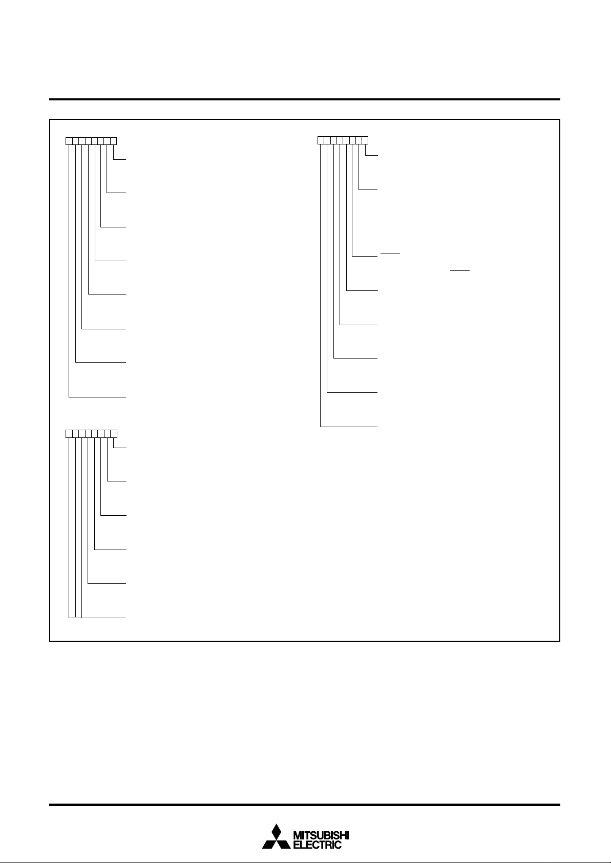
PRELIMINARY
Notice: This is not a final specification.
Some parametric limits are subject to change.
MITSUBISHI MICROCOMPUTERS
7540 Group
SINGLE-CHIP 8-BIT CMOS MICROCOMPUTER
b7
b0
Serial I/O1 status register
(SIO1STS : address 001916)
b7
Transmit buffer empty flag (TBE)
0: Buffer full
1: Buffer empty
Receive buffer full flag (RBF)
0: Buffer empty
1: Buffer full
Transmit shift completion flag (TSC)
0: Transmit shift in progress
1: Transmit shift completed
Overrun error flag (OE)
0: No error
1: Overrun error
Parity error flag (PE)
0: No error
1: Parity error
Framing error flag (FE)
0: No error
1: Framing error
Summing error flag (SE)
0: (OE) U (PE) U (FE)=0
1: (OE) U (PE) U (FE)=1
Not used (returns “1” when read)
b0
Serial I/O1 control register
(SIO1CON : address 001A
16
)
BRG count source selection bit (CSS)
IN
)
0: f(X
IN
)/4
1: f(X
Serial I/O1 synchronous clock selection bit (SCS)
0: BRG output divided by 4 when clock synchronous
serial I/O is selected, BRG output divided by 16
when UART is selected.
1: External clock input when clock synchronous serial
I/O is selected, external clock input divided by 16
when UART is selected.
RDY1
output enable bit (SRDY)
S
3
pin operates as ordinary I/O pin
0: P1
3
pin operates as S
1: P1
RDY1
output pin
Transmit interrupt source selection bit (TIC)
0: Interrupt when transmit buffer has emptied
1: Interrupt when transmit shift operation is completed
Transmit enable bit (TE)
0: Transmit disabled
1: Transmit enabled
Receive enable bit (RE)
0: Receive disabled
1: Receive enabled
Serial I/O1 mode selection bit (SIOM)
0: Clock asynchronous (UART) serial I/O
1: Clock synchronous serial I/O
b7
b0
UART control register
(UARTCON : address 001B
Character length selection bit (CHAS)
0: 8 bits
1: 7 bits
Serial I/O1 enable bit (SIOE)
16
)
0: Serial I/O1 disabled
0
(pins P1
to P13 operate as ordinary I/O pins)
1: Serial I/O1 enabled
0
(pins P1
to P13operate as serial I/O pins)
Parity enable bit (PARE)
0: Parity checking disabled
1: Parity checking enabled
Parity selection bit (PARS)
0: Even parity
1: Odd parity
Stop bit length selection bit (STPS)
0: 1 stop bit
1: 2 stop bits
1/TXD1
P-channel output disable bit (POFF)
P1
0: CMOS output (in output mode)
1: N-channel open drain output (in output mode)
Not used (return “1” when read)
Fig. 31 Structure of serial I/O1-related registers
30
Page 31

PRELIMINARY
Notice: This is not a final specification.
Some parametric limits are subject to change.
MITSUBISHI MICROCOMPUTERS
7540 Group
SINGLE-CHIP 8-BIT CMOS MICROCOMPUTER
●Serial I/O2
The serial I/O2 function can be used only for clock synchronous serial I/O.
For clock synchronous serial I/O2 the transmitter and the receiver
must use the same clock. When the internal clock is used, transfer is
started by a write signal to the serial I/O2 register.
Note: Serial I/O2 can be used in the following cases;
(1) Serial I/O1 is not used,
(2) Serial I/O1 is used as UART and BRG output divided by 16 is
selected as the synchronized clock.
[Serial I/O2 control register] SIO2CON
The serial I/O2 control register contains 8 bits which control various
serial I/O functions.
• Set “0” to bit 3 to receive.
• At reception, clear bit 7 to “0” by writing a dummy data to the serial
I/O2 register after completion of shift.
b7 b0
Serial I/O2 control register
(SIO2CON: address 0030
Internal synchronous clock selection bits
000 : f(X
001 : f(X
010 : f(X
011 : f(X
110 : f(X
111 : f(X
S
DATA2
0 : I/O port / S
1 : S
IN
)/8
IN
)/16
IN
)/32
IN
)/64
IN
)/128
IN
)/256
pin selection bit (Note)
DATA2
DATA2
output
Not used
(returns “0” when read)
Transfer direction selection bit
0 : LSB first
1 : MSB first
S
CLK2
pin selection bit
0 : External clock (S
1 : Internal clock (S
CLK2
CLK2
Transmit / receive shift completion flag
0 : shift in progress
1 : shift completed
Note : When using it as a S
DATA
input, set the port P13
direction register to “0”.
Fig. 32 Structure of serial I/O2 control registers
16
)
input
is an input)
is an output)
XIN
P12/SCLK2
P13/SDATA2
CLK2 pin selection bit
S
“0”
P12 latch
“1”
SDATA2 pin selection bit
“0”
P13 latch
“1”
DATA2 pin selection bit
S
SCLK
SCLK2 pin
selection bit
1/8
1/16
1/32
1/64
Divider
1/128
1/256
“1”
Internal synchronous
clock selection bits
“0”
Serial I/O counter 2 (3)
Serial I/O shift register 2 (8)
Data bus
Serial I/O2
interrupt request
Fig. 33 Block diagram of serial I/O2
31
Page 32

PRELIMINARY
Notice: This is not a final specification.
Some parametric limits are subject to change.
Serial I/O2 operation
By writing to the serial I/O2 register (address 003116) the serial I/O2
counter is set to “7”.
After writing, the SDATA2 pin outputs data every time the transfer
clock shifts from “H” to “L”. And, as the transfer clock shifts from “L”
to “H”, the SDATA2 pin reads data, and at the same time the contents
of the serial I/O2 register are shifted by 1 bit.
When the internal clock is selected as the transfer clock source, the
following operations execute as the transfer clock counts up to 8.
• Serial I/O2 counter is cleared to “0”.
• Transfer clock stops at an “H” level.
• Interrupt request bit is set.
• Shift completion flag is set.
Also, the SDATA2 pin is in a high impedance state after the data transfer
is completed.
When the external clock is selected as the transfer clock source, the
interrupt request bit is set as the transfer clock counts up to 8, but
external control of the clock is required since it does not stop. Notice
that the SDATA2 pin is not in a high impedance state on the completion of data transfer.
Also, after the receive operation is completed, the transmit/receive
shift completion flag is cleared by reading the serial I/O2 register. At
transmit, the transmit/receive shift completion flag is cleared and the
transmit operation is started by writing to serial I/O2 register.
MITSUBISHI MICROCOMPUTERS
7540 Group
SINGLE-CHIP 8-BIT CMOS MICROCOMPUTER
Synchronous clock
Transfer clock
Serial I/O2 register
write signal
DATA2
at serial I/O2
S
output transmit
S
DATA2
at serial I/O2
input receive
: When the internal clock is selected as the transfer, the S
Fig. 34 Serial I/O2 timing (LSB first)
(Note)
D
0
D
1
D
2
D
3
D
4
D
5
D6D
7
Serial I/O2 interrupt request bit set
Transmit/receive shift completion flag set
DATA2
pin is in a high impedance state after the data transfer is completed.Note
32
Page 33

PRELIMINARY
Notice: This is not a final specification.
Some parametric limits are subject to change.
MITSUBISHI MICROCOMPUTERS
7540 Group
SINGLE-CHIP 8-BIT CMOS MICROCOMPUTER
A-D Converter
The functional blocks of the A-D converter are described below.
[A-D conversion register] AD
The A-D conversion register is a read-only register that stores the
result of A-D conversion. Do not read out this register during an A-D
conversion.
[A-D control register] ADCON
The A-D control register controls the A-D converter. Bit 2 to 0 are
analog input pin selection bits. Bit 4 is the AD conversion completion
bit. The value of this bit remains at “0” during A-D conversion, and
changes to “1” at completion of A-D conversion.
A-D conversion is started by setting this bit to “0”.
[Comparison voltage generator]
The comparison voltage generator divides the voltage between AVSS
and VREF by 1024, and outputs the divided voltages.
[Channel selector]
The channel selector selects one of ports P27/AN7 to P20/AN0, and
inputs the voltage to the comparator.
[Comparator and control circuit]
The comparator and control circuit compares an analog input voltage with the comparison voltage and stores its result into the A-D
conversion register. When A-D conversion is completed, the control
circuit sets the AD conversion completion bit and the AD interrupt
request bit to “1”. Because the comparator is constructed linked to a
capacitor, set f(XIN) to 500 kHz or more during A-D conversion.
b7 b0
A-D control register
(ADCON : address 0034
Analog input pin selection bits
000 : P2
001 : P21/AN
010 : P22/AN
011 : P23/AN
100 : P24/AN
101 : P25/AN
110 : P26/AN6 (Note)
111 : P2
Not used (returns “0” when read)
AD conversion completion bit
0 : Conversion in progress
1 : Conversion completed
Not used (returns “0” when read)
Note: These can be used only for 36 pin version.
0
/AN
7
/AN7 (Note)
16
0
1
2
3
4
5
Fig. 35 Structure of A-D control register
Read 8-bit (Read only address 003516)
b7 b0
(Address 003516)
Read 10-bit (read in order address 003616, 003516)
(Address 003616)
(Address 003516)
Note: High-order 6-bit of address 003616 returns “0” when read.
b9 b8 b7 b6 b5 b4 b3 b2
b7
b7
b7 b6 b5 b4 b3 b2 b1 b0
)
b0
b9 b8
b0
Data bus
A-D control register
(Address 0034
P20/AN
0
P21/AN
1
P22/AN
2
P23/AN
3
P24/AN
4
P25/AN
5
P26/AN
P27/AN
6
7
Channel selector
Fig. 37 Block diagram of A-D converter
b7 b0
16
)
3
A-D control circuit
Comparator
A-D conversion register (high-order)
A-D conversion register (low-order)
Resistor ladder
V
REF
Fig. 36 Structure of A-D conversion register
A-D interrupt request
(Address 0036
(Address 0035
10
V
SS
16
)
16
)
33
Page 34
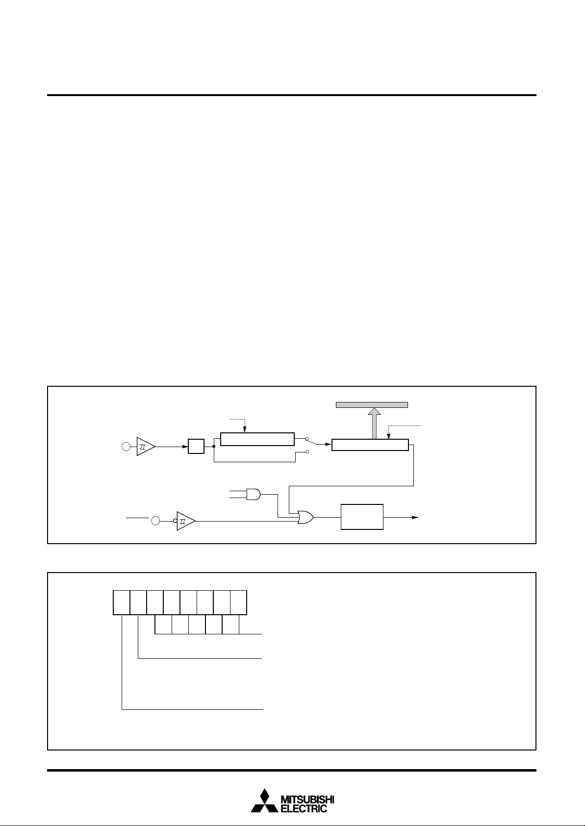
PRELIMINARY
Notice: This is not a final specification.
Some parametric limits are subject to change.
MITSUBISHI MICROCOMPUTERS
7540 Group
SINGLE-CHIP 8-BIT CMOS MICROCOMPUTER
Watchdog Timer
The watchdog timer gives a means for returning to a reset status
when the program fails to run on its normal loop due to a runaway.
The watchdog timer consists of an 8-bit watchdog timer H and an 8bit watchdog timer L, being a 16-bit counter.
Standard operation of watchdog timer
The watchdog timer stops when the watchdog timer control register
(address 003916) is not set after reset. Writing an optional value to
the watchdog timer control register (address 003916) causes the
watchdog timer to start to count down. When the watchdog timer H
underflows, an internal reset occurs. Accordingly, it is programmed
that the watchdog timer control register (address 003916) can be set
before an underflow occurs.
When the watchdog timer control register (address 003916) is read,
the values of the high-order 6-bit of the watchdog timer H, STP instruction disable bit and watchdog timer H count source selection bit
are read.
Initial value of watchdog timer
By a reset or writing to the watchdog timer control register (address
003916), the watchdog timer H is set to “FF16” and the watchdog
timer L is set to “FF16”.
Operation of watchdog timer H count source selection bit
A watchdog timer H count source can be selected by bit 7 of the
watchdog timer control register (address 003916). When this bit is
“0”, the count source becomes a watchdog timer L underflow signal.
The detection time is 131.072 ms at f(XIN)=8 MHz.
When this bit is “1”, the count source becomes f(XIN)/16. In this
case, the detection time is 512 µs at f(XIN)=8 MHz.
This bit is cleared to “0” after reset.
Operation of STP instruction disable bit
When the watchdog timer is in operation, the STP instruction can be
disabled by bit 6 of the watchdog timer control register (address
003916).
When this bit is “0”, the STP instruction is enabled.
When this bit is “1”, the STP instruction is disabled, and an internal
reset occurs if the STP instruction is executed.
Once this bit is set to “1”, it cannot be changed to “0” by program.
This bit is cleared to “0” after reset.
Write “FF
watchdog timer
control register
XIN
STP Instruction disable bit
RESET
Fig. 38 Block diagram of watchdog timer
1/16
STP Instruction
b7 b0
16” to the
Watchdog timer L (8)
Data bus
Write "FF
16" to the
“0”
“1”
Watchdog timer H count
source selection bit
Watchdog timer H (8)
Reset
circuit
watchdog timer
control register
Internal reset
Watchdog timer control register
16
(WDTCON: address 0039
)
Watchdog timer H (read only for high-order 6-bit)
STP instruction disable bit
0 : STP instruction enabled
1 : STP instruction disabled
Fig. 39 Structure of watchdog timer control register
34
Watchdog timer H count source selection bit
0 : Watchdog timer L underflow
IN
1 : f(X
)/16
Page 35

PRELIMINARY
Notice: This is not a final specification.
Some parametric limits are subject to change.
MITSUBISHI MICROCOMPUTERS
7540 Group
SINGLE-CHIP 8-BIT CMOS MICROCOMPUTER
Reset Circuit
The microcomputer is put into a reset status by holding the RESET
______
pin at the “L” level for 2 µs or more when the power source voltage is
2.2 to 5.5 V and XIN is in stable oscillation.
After that, this reset status is released by returning the RESET pin to
______
the “H” level. The program starts from the address having the contents of address FFFD16 as high-order address and the contents of
address FFFC16 as low-order address.
In the case of f(φ) ≤ 4 MHz, the reset input voltage must be 0.8 V or
less when the power source voltage passes 4.0 V.
In the case of f(φ) ≤ 2 MHz, the reset input voltage must be 0.48 V or
less when the power source voltage passes 2.4 V.
In the case of f(φ) ≤ 1 MHz, the reset input voltage must be 0.44 V or
less when the power source voltage passes 2.2 V.
Power source
voltage
V
RESET
RESET
CC
0 V
Reset input
voltage
0 V
Note : Reset release voltage Vcc = 2.2 V
V
CC
Fig. 40 Example of reset circuit
Poweron
(Note)
0.2 V
CC
Power source
voltage
detection circuit
Clock from built-in
ring oscillator RING
f
RESET
OUT
RESET
SYNC
Address
Data
Fig. 41 Timing diagram at reset
??
8-13 clock cycles
???
?? ADLAD
Notes
???
1 : A built-in ring oscillator applies about RING•2 MHz, f•250 kHz frequency clock
at average of Vcc = 5 V.
2 : The mark “?” means that the address is changeable depending on the previous state.
3 : These are all internal signals except RESET.
FFFC FFFD
ADH,AD
H
L
Reset address from the
vector table
35
Page 36

PRELIMINARY
Notice: This is not a final specification.
Some parametric limits are subject to change.
MITSUBISHI MICROCOMPUTERS
7540 Group
SINGLE-CHIP 8-BIT CMOS MICROCOMPUTER
(1)
Port P0 direction register
(2)
Port P1 direction register
(3)
Port P2 direction register
(4)
Port P3 direction register
(5)
Pull-up control register
(6)
Port P1P3 control register
(7)
Serial I/O1 status register
(8)
Serial I/O1 control register
(9)
UART control register
(10)
Timer A mode register
(11)
Timer A (low-order)
(12)
Timer A (high-order)
(13)
Timer Y, Z mode register
(14)
Prescaler Y
(15)
Timer Y secondary
(16)
Timer Y primary
(17)
Timer Y, Z waveform output control register
(18)
Prescaler Z
(19)
Timer Z secondary
(20)
Timer Z primary
(21)
Prescaler 1
(22)
Timer 1
(23)
One-shot start register
(24)
Timer X mode register
(25)
Prescaler X
(26)
Timer X
Timer count source set register
(27)
Serial I/O2 control register
(28)
Serial I/O2 register
(29)
(30)
A-D control register
(31)
MISRG
(32)
Watchdog timer control register
(33)
Interrupt edge selection register
(34)
CPU mode register
(35)
Interrupt request register 1
(36)
Interrupt request register 2
(37)
Interrupt control register 1
Interrupt control register 2
(38)
Processor status register
(39)
Program counter
(40)
Address
0001
16
0003
16
0005
16
0007
16
0016
16
0017
16
0019
16
16
001A
001B
16
001D
16
001E
16
001F
16
0020
16
0021
16
0022
16
0023
16
0024
16
0025
16
0026
16
0027
16
0028
16
0029
16
002A
16
002B
16
002C
16
002D
16
002E
16
16
0030
0031
16
16
0034
0038
16
0039
16
003A
16
16
003B
003C
16
003D
16
003E
16
16
003F
(PS)
(PCH)
L
)
(PC
Register contents
0016
XXX0 0000
0016
0016
0016
16
00
10000001
0216
11100000
0016
FF16
FF16
0016
FF16
FF16
FF16
0016
FF16
FF16
FF16
FF16
0116
0016
0016
FF16
FF16
0016
0016
0016
1016
0016
00111111
0016
10000000
0016
0016
0016
0016
XXXXX1XX
Contents of address FFFD
Contents of address FFFC
Note X : Undefined
16
16
Fig. 42 Internal status of microcomputer at reset
36
Page 37

PRELIMINARY
Notice: This is not a final specification.
Some parametric limits are subject to change.
MITSUBISHI MICROCOMPUTERS
7540 Group
SINGLE-CHIP 8-BIT CMOS MICROCOMPUTER
Clock Generating Circuit
An oscillation circuit can be formed by connecting a resonator between XIN and XOUT, and an RC oscillation circuit can be formed by
connecting a resistor and a capacitor.
Use the circuit constants in accordance with the resonator
manufacturer's recommended values. No external resistor is needed
between XIN and XOUT since a feed-back resistor exists on-chip.
Set the constants of the resistor and capacitor when an RC oscillator
is used, so that a frequency variation due to LSI variation and resistor and capacitor variations may not exceed the standard input frequency.
●Oscillation control
• Stop mode
When the STP instruction is executed, the internal clock f stops at
an “H” level and the XIN oscillator stops. At this time, timer 1 is set
to “0116” and prescaler 1 is set to “FF16” when the oscillation stabilization time set bit after release of the STP instruction is “0”. On the
other hand, timer 1 and prescaler 1 are not set when the above bit
is “1”. Accordingly, set the wait time fit for the oscillation stabilization time of the oscillator to be used. f(XIN)/16 is forcibly connected
to the input of prescaler 1. When an external interrupt is accepted,
oscillation is restarted but the internal clock f remains at “H” until
timer 1 underflows. As soon as timer 1 underflows, the internal
clock f is supplied. This is because when a ceramic oscillator is
used, some time is required until a start of oscillation. In case oscillation is restarted by reset, no wait time is generated. So apply an
“L” level to the RESET pin while oscillation becomes stable.
Also, the STP instruction cannot be used while CPU is operating by
a ring oscillator.
●Switch of ceramic and RC oscillations
After releasing reset the operation starts by starting a built-in ring
oscillator. Then, a ceramic oscillation or an RC oscillation is selected
by setting bit 5 of the CPU mode register.
●Double-speed mode
When a ceramic oscillation is selected, a double-speed mode can be
used. Do not use it when an RC oscillation is selected.
●CPU mode register
Bits 5, 1 and 0 of CPU mode register are used to select oscillation
mode and to control operation modes of the microcomputer. In order
to prevent the dead-lock by error-writing (ex. program run-away), these
bits can be rewritten only once after releasing reset. After rewriting it
is disable to write any data to the bit. (The emulator MCU
“M37540RSS” is excluded.)
Also, when the read-modify-write instructions (SEB, CLB) are executed to bits 2 to 4, 6 and 7, bits 5, 1 and 0 are locked.
●Clock division ratio, XIN oscillation control,
ring oscillator control
The state transition shown in Fig. 49 can be performed by setting the
clock division ratio selection bits (bits 7 and 6), XIN oscillation control
bit (bit 4), ring oscillator oscillation control bit (bit 3) of CPU mode
register. Be careful of notes on use in Fig. 49.
• Wait mode
If the WIT instruction is executed, the internal clock f stops at an “H”
level, but the oscillator does not stop. The internal clock restarts if
a reset occurs or when an interrupt is received. Since the oscillator
does not stop, normal operation can be started immediately after
the clock is restarted. To ensure that interrupts will be received to
release the STP or WIT state, interrupt enable bits must be set to
“1” before the STP or WIT instruction is executed.
When the STP status is released, prescaler 1 and timer 1 will start
counting clock which is XIN divided by 16, so set the timer 1 interrupt enable bit to “0” before the STP instruction is executed.
Note
For use with the oscillation stabilization set bit after release of the
STP instruction set to “1”, set values in timer 1 and prescaler
1 after fully appreciating the oscillation stabilization time of the
oscillator to be used.
37
Page 38

PRELIMINARY
Notice: This is not a final specification.
Some parametric limits are subject to change.
XIN
C
IN
Fig. 43 External circuit of ceramic resonator
X
OUT
MITSUBISHI MICROCOMPUTERS
7540 Group
SINGLE-CHIP 8-BIT CMOS MICROCOMPUTER
b7 b0
MISRG(address 003816)
Oscillation stabilization time set bit after
release of the STP instruction
0: Set “01
in prescaler 1 automatically
1: Not set automatically
Reserved bits (return “0” when read)
(Do not write “1” to these bits)
Not used (return “0” when read)
C
OUT
Fig. 46 Structure of MISRG
16
” in timer1, and “FF16”
X
IN XOUT
Fig. 44 External circuit of RC oscillation
XIN
External oscillation
circuit
CC
V
V
SS
X
OUT
Open
R
C
Fig. 45 External clock input circuit
38
Page 39

PRELIMINARY
Notice: This is not a final specification.
Some parametric limits are subject to change.
X
IN
MITSUBISHI MICROCOMPUTERS
7540 Group
SINGLE-CHIP 8-BIT CMOS MICROCOMPUTER
X
OUT
Rf
Ring oscillator
(Note)
SRQ
STP instruction
Rd
1/2
High-speed mode
Double-speed mode
1/8
Ring oscillator mode
instruction
1/4
WIT
1/2
Main clock division
ratio selection bit
Middle-speed mode
Q
S
R
Reset
Interrupt disable flag l
Interrupt request
Note: Ring oscillator is used only for starting.
Fig. 47 Block diagram of internal clock generating circuit (for ceramic resonator)
Prescaler 1
S
Q
R
Timer 1
Timing φ
(Internal clock)
STP instruction
X
OUT
Delay
X
IN
Ring oscillator
(Note)
SRQ
STP instruction
1/2
High-speed mode
Double-speed mode
1/8
Ring oscillator mode
instruction
1/4
WIT
1/2
Main clock division
ratio selection bit
Middle-speed mode
S
R
Reset
Interrupt disable flag l
Interrupt request
Fig. 48 Block diagram of internal clock generating circuit (for RC oscillation)
Prescaler 1
Timer 1
Timing φ
(Internal clock)
Q
Note: Ring oscillator is used only for starting.
S
Q
R
STP instruction
39
Page 40

PRELIMINARY
Notice: This is not a final specification.
Some parametric limits are subject to change.
CM4←1
MITSUBISHI MICROCOMPUTERS
7540 Group
SINGLE-CHIP 8-BIT CMOS MICROCOMPUTER
2
State 1
Operation clock source: X
X
IN
oscillation enabled
Ring oscillator stop
CM3←1
CM7,6←NOT(102)
2
CM4←0
CM3←1
2
CM7,6←10
2
CM4←1
2
Notes on switch of clock
(1) Execute the state transition from state 3 to state 2 after stabilizing X
(2) Do not execute the state transition shown
(3) In operation clock source = X
middle-speed mode can be selected for the CPU clock division ratio.
(4) In operation clock source = ring oscillator, the middle-speed mode is selected for
the CPU clock division ratio.
(5) Do not stop the clock selected as the operation clock because of setting of CM3, 4.
IN
CM7,6←10
CM3←0
2
2
State 2
Operation clock source: X
X
IN
oscillation enabled
Ring oscillator enalbed
CM7,6←NOT(102)
CM7,6←NOT(102)
CM4←0
IN, the double-speed mode, high-speed mode, and
IN
2
.
2
CM3←0
2
CM4←1
2
CM7,6←10
State 3 (initial state after reset)
Operation clock source: Ring oscillator
IN
oscillation enabled
X
Ring oscillator enalbed
IN oscillation.
2
CM4←0
CM7,6←10
CM4←1
CM3←0
CM7,6←NOT(102)
2
CM3←1
CM3←1
2
State 4 (low power dissipation mode
2
2
2
2
CM4←1
2
by ring oscillator)
Operation clock source: Ring oscillator
IN
oscillation stop
X
Ring oscillator enalbed
CM3←1
2
Fig. 49 State transition
40
Page 41

PRELIMINARY
Notice: This is not a final specification.
Some parametric limits are subject to change.
MITSUBISHI MICROCOMPUTERS
7540 Group
SINGLE-CHIP 8-BIT CMOS MICROCOMPUTER
NOTES ON PROGRAMMING
Processor Status Register
The contents of the processor status register (PS) after reset are
undefined except for the interrupt disable flag I which is “1”. After
reset, initialize flags which affect program execution. In particular, it
is essential to initialize the T flag and the D flag because of their
effect on calculations.
Interrupts
The contents of the interrupt request bit do not change even if the
BBC or BBS instruction is executed immediately after they are
changed by program because this instruction is executed for the previous contents. For executing the instruction for the changed contents, execute one instruction before executing the BBC or BBS instruction.
Decimal Calculations
• For calculations in decimal notation, set the decimal mode flag D to
“1”, then execute the ADC instruction or SBC instruction. In this
case, execute SEC instruction, CLC instruction or CLD instruction
after executing one instruction before the ADC instruction or SBC
instruction.
• In the decimal mode, the values of the N (negative), V (overflow)
and Z (zero) flags are invalid.
A-D Converter
The comparator uses internal capacitors whose charge will be lost if
the clock frequency is too low.
Make sure that f(XIN) is 500kHz or more during A-D conversion.
Do not execute the STP instruction during A-D conversion.
Instruction Execution Timing
The instruction execution time can be obtained by multiplying the
frequency of the internal clock φ by the number of cycles mentioned
in the machine-language instruction table.
The frequency of the internal clock φ is the same as that of the XIN in
double-speed mode, twice the XIN cycle in high-speed mode and 8
times the XIN cycle in middle-speed mode.
CPU Mode Register
The oscillation mode selection bit and processor mode bits can be
rewritten only once after releasing reset. However, after rewriting it is
disable to write any value to the bit. (Emulator MCU is excluded.)
When a ceramic oscillation is selected, a double-speed mode of the
clock division ratio selection bits can be used. Do not use it when an
RC oscillation is selected.
State transition
Do not stop the clock selected as the operation clock because of
setting of CM3, 4.
Timers
• When n (0 to 255) is written to a timer latch, the frequency division
ratio is 1/(n+1).
• When a count source of timer X, timer Y or timer Z is switched, stop
a count of timer X.
Ports
• The values of the port direction registers cannot be read.
That is, it is impossible to use the LDA instruction, memory operation instruction when the T flag is “1”, addressing mode using direction register values as qualifiers, and bit test instructions such
as BBC and BBS.
It is also impossible to use bit operation instructions such as CLB
and SEB and read/modify/write instructions of direction registers
for calculations such as ROR.
For setting direction registers, use the LDM instruction, STA instruction, etc.
• P26/AN6, P27/AN7, P35 (LED5), P36/INT1 pins do not exist in the
32-pin version. Stabilize the internal level by setting the port direction registers of these ports to output or setting P35, P36 pull-up
control bits of the pull-up control register (PULL) to ON by program.
NOTES ON USE
Handling of Power Source Pin
In order to avoid a latch-up occurrence, connect a capacitor suitable
for high frequencies as bypass capacitor between power source pin
(Vcc pin) and GND pin (Vss pin). Besides, connect the capacitor to
as close as possible. For bypass capacitor which should not be located too far from the pins to be connected, a ceramic capacitor of
0.01 µF to 0.1 µF is recommended.
One Time PROM Version
The CNVss pin is connected to the internal memory circuit block by a
low-ohmic resistance, since it has the multiplexed function to be a
programmable power source pin (VPP pin) as well.
To improve the noise reduction, connect a track between CNVss pin
and Vss pin with 1 to 10 kΩ resistance.
The mask ROM version track of CNVss pin has no operational interference even if it is connected via a resistor.
41
Page 42

PRELIMINARY
Notice: This is not a final specification.
Some parametric limits are subject to change.
MITSUBISHI MICROCOMPUTERS
7540 Group
SINGLE-CHIP 8-BIT CMOS MICROCOMPUTER
DATA REQUIRED FOR MASK ORDERS
The following are necessary when ordering a mask ROM production:
(1) Mask ROM Order Confirmation Form
(2) Mark Specification Form
(3) Data to be written to ROM, in EPROM form
(three identical copies)
ROM PROGRAMMING METHOD
The built-in PROM of the blank One Time PROM version can be
read or programmed with a general-purpose PROM programmer using a special programming adapter. Set the address of PROM programmer in the user ROM area.
Table 5 Special programming adapter
Package
32P4B
32P6B-A
36P2R-A
The PROM of the blank One Time PROM version is not tested or
screened in the assembly process and following processes. To ensure proper operation after programming, the procedure shown in
Figure 50 is recommended to verify programming.
Programming with
PROM programmer
Screening (Caution)
(150 °C for 40 hours)
Name of Programming Adapter
PCA7435SPG02
PCA7435GPG02
PCA7435FPG02
Verification with PROM
programmer
Functional check in
target device
Caution:
Fig. 50 Programming and testing of One Time PROM version
The screening temperature is far higher
than the storage temperature. Never
expose to 150 °C exceeding 100 hours.
42
Page 43
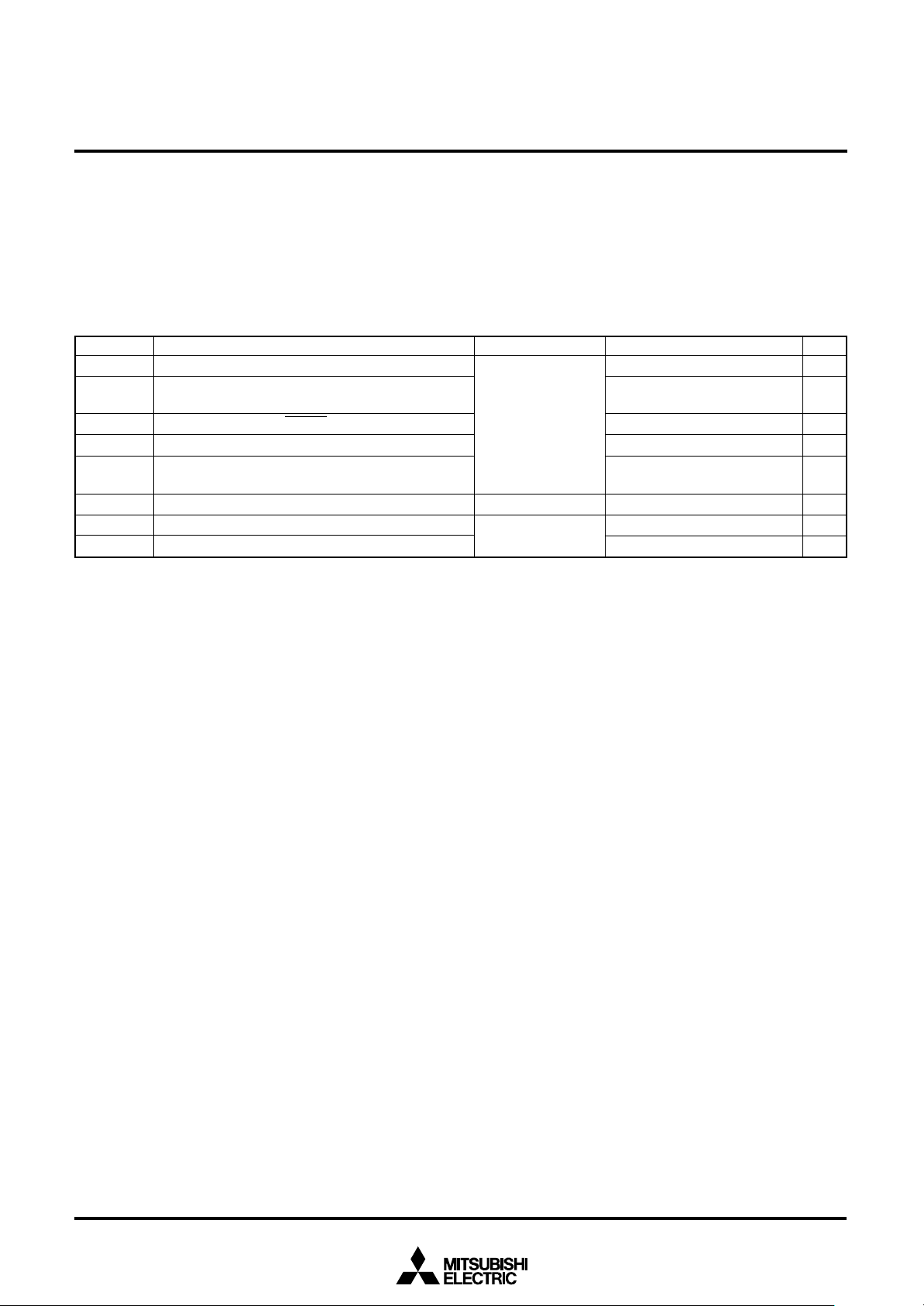
MITSUBISHI MICROCOMPUTERS
PRELIMINARY
Notice: This is not a final specification.
Some parametric limits are subject to change.
ELECTRICAL CHARACTERISTICS
1.7540Group (General purpose)
Applied to: M37540M4-XXXFP/SP/GP, M37540E8FP/SP/GP
Absolute Maximum Ratings (General purpose)
Table 6 Absolute maximum ratings
Symbol
VCC
VI
VI
VI
VO
Pd
Topr
Tstg
Note 1:It is a rating only for the One Time PROM version. Connect to VSS for the mask ROM version.
2: 200 mW for the 32P6B package product.
Power source voltage
Input voltage P00–P07, P10–P14, P20–P27,
Input voltage RESET, XIN
Input voltage CNVSS (Note 1)
Output voltage P00–P07, P10–P14, P20–P27,
Power dissipation
Operating temperature
Storage temperature
Parameter
P30–P37, VREF
P30–P37, XOUT
All voltages are
based on VSS.
Output transistors
are cut off.
Ta = 25°C
SINGLE-CHIP 8-BIT CMOS MICROCOMPUTER
Conditions
7540 Group
Ratings
–0.3 to 7.0
–0.3 to VCC + 0.3
–0.3 to VCC + 0.3
–0.3 to 13
–0.3 to VCC + 0.3
300 (Note 2)
–20 to 85
–40 to 125
Unit
V
V
V
V
V
mW
°C
°C
43
Page 44

MITSUBISHI MICROCOMPUTERS
7540 Group
PRELIMINARY
Notice: This is not a final specification.
Some parametric limits are subject to change.
Recommended Operating Conditions (General purpose)
Table 7 Recommended operating conditions (1) (VCC = 2.2 to 5.5 V, Ta = –20 to 85 °C, unless otherwise noted)
Symbol Parameter Unit
VCC
VSS
VREF
VIH
VIH
VIH
VIL
VIL
VIL
VIL
∑IOH(peak)
∑IOL(peak)
∑IOL(peak)
∑IOH(avg)
∑IOL(avg)
∑IOL(avg)
Note 1: Vcc = 4.0 to 5.5V
2: The total output current is the sum of all the currents flowing through all the applicable ports. The total average current is an average
Power source voltage
Power source voltage (RC)
Power source voltage
Analog reference voltage
“H” input voltage P00–P07, P10–P14, P20–P27,
“H” input voltage (TTL input level selected) P10, P12, P13, P36, P37 (Note 1)
“H” input voltage RESET, XIN
“L” input voltage P00–P07, P10–P14, P20–P27,
“L” input voltage (TTL input level selected) P10, P12, P13, P36, P37 (Note 1)
“L” input voltage RESET, CNVSS
“L” input voltage XIN
“H” total peak output current (Note 2) P00–P07, P10–P14, P20–P27,
“L” total peak output current (Note 2) P00–P07, P10–P14, P20–P27,
“L” total peak output current (Note 2) P30–P36
“H” total average output current (Note 2) P00–P07, P10–P14, P20–P27,
“L” total average output current (Note 2) P00–P07, P10–P14, P20–P27,
“L” total average output current (Note 2) P30–P36
value measured over 100 ms. The total peak current is the peak value of all the currents.
(ceramic)
f(XIN) =
8 MHz (High-, Middle-speed mode)
f(XIN) =
4 MHz (High-, Middle-speed mode)
f(XIN) = 2 MHz
f(XIN) = 4 MHz (Doublef(XIN) = 2 MHz (Doublef(XIN) = 1 MHz (Doublef(XIN) = 4 MHz (
f(XIN) = 2 MHz (
f(XIN) = 1 MHz (
(High-, Middle-speed mode)
speed mode
speed mode
speed mode
High-, Middle-speed mode
High-, Middle-speed mode
High-, Middle-speed mode
P30–P37
P30–P37
P30–P37
P37
P30–P37
P37
SINGLE-CHIP 8-BIT CMOS MICROCOMPUTER
Limits
Min.
4.0
2.4
2.2
)
)
)
)
)
)
4.0
2.4
2.2
4.0
2.4
2.2
2.0
0.8VCC
2.0
0.8VCC
0
0
0
0
Typ. Max.
5.0
5.0
5.0
5.0
5.0
5.0
5.0
5.0
5.0
0
5.5
5.5
5.5
5.5
5.5
5.5
5.5
5.5
5.5
VCC
VCC
VCC
VCC
0.3VCC
0.8
0.2VCC
0.16VCC
–80
80
60
–40
40
30
V
V
V
V
V
V
V
V
V
V
V
V
V
V
V
V
V
V
mA
mA
mA
mA
mA
mA
44
Page 45
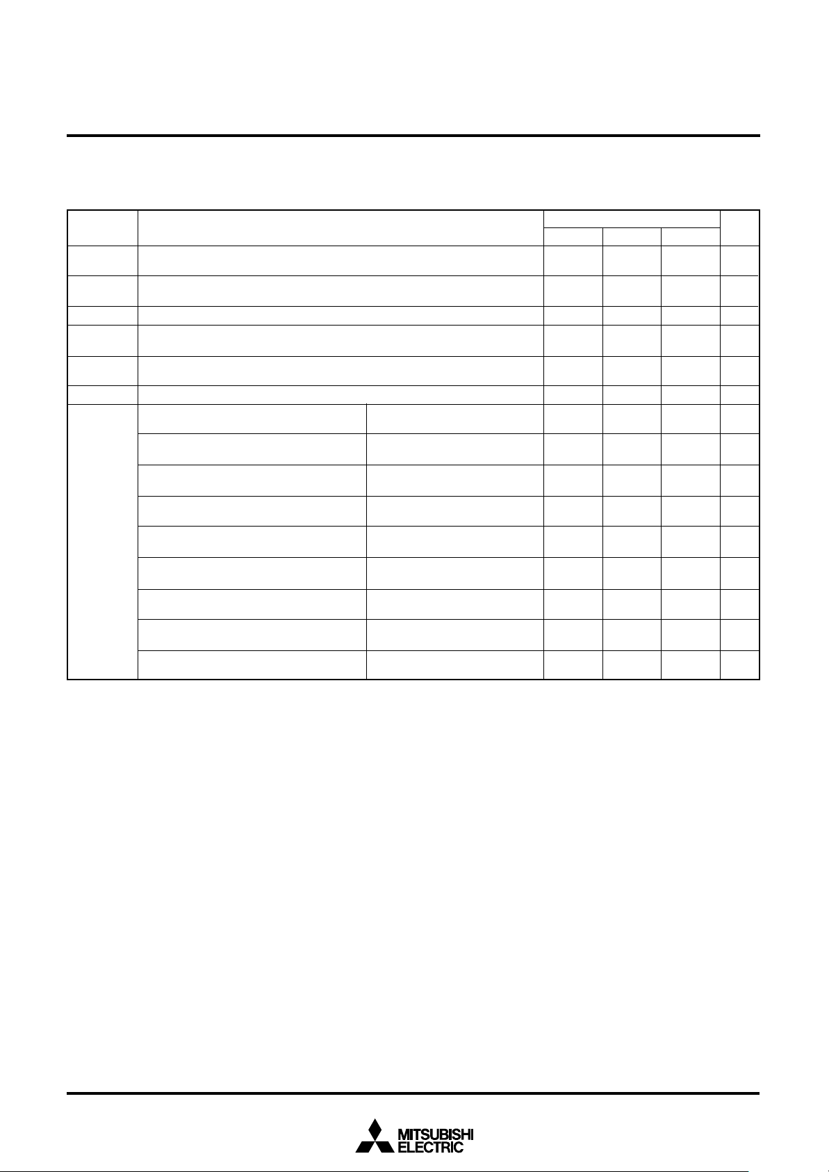
MITSUBISHI MICROCOMPUTERS
PRELIMINARY
Notice: This is not a final specification.
Some parametric limits are subject to change.
Recommended Operating Conditions (General purpose)(continued)
Table 8 Recommended operating conditions (2) (VCC = 2.2 to 5.5 V, Ta = –20 to 85 °C, unless otherwise noted)
Symbol Parameter
IOH(peak)
IOL(peak)
IOL(peak)
IOH(avg)
IOL(avg)
IOL(avg)
f(XIN)
Notes 1: The peak output current is the peak current flowing in each port.
2: The average output current IOL (avg), IOH (avg) in an average value measured over 100 ms.
3: When the oscillation frequency has a duty cycle of 50 %.
“H” peak output current (Note 1) P00–P07, P10–P14, P20–P27,
P30–P37
“L” peak output current (Note 1) P00–P07, P10–P14, P20–P27,
P37
“L” peak output current (Note 1) P30–P36
“H” average output current (Note 2) P00–P07, P10–P14, P20–P27,
P30–P37
“L” average output current (Note 2) P00–P07, P10–P14, P20–P27,
P37
“L” average output current (Note 2) P30–P36
Internal clock oscillation frequency (Note 3) VCC = 4.0 to 5.5 V
at ceramic oscillation or external clock input Double-speed mode
Internal clock oscillation frequency (Note 3) VCC = 2.4 to 5.5 V
at ceramic oscillation or external clock input Double-speed mode
Internal clock oscillation frequency (Note 3) VCC = 2.2 to 5.5 V
at ceramic oscillation or external clock input Double-speed mode
Internal clock oscillation frequency (Note 3) VCC = 4.0 to 5.5 V
at ceramic oscillation or external clock input High-, Middle-speed mode
Internal clock oscillation frequency (Note 3) VCC = 2.4 to 5.5 V
at ceramic oscillation or external clock input High-, Middle-speed mode
Internal clock oscillation frequency (Note 3) VCC = 2.2 to 5.5 V
at ceramic oscillation or external clock input High-, Middle-speed mode
Internal clock oscillation frequency (Note 3) VCC = 4.0 to 5.5 V
at RC oscillation High-, Middle-speed mode
Internal clock oscillation frequency (Note 3) VCC = 2.4 to 5.5 V
at RC oscillation High-, Middle-speed mode
Internal clock oscillation frequency (Note 3) VCC = 2.2 to 5.5 V
at RC oscillation High-, Middle-speed mode
SINGLE-CHIP 8-BIT CMOS MICROCOMPUTER
Limits
7540 Group
Max.Typ.Min.
–10
10
30
–5
5
15
4
2
1
8
4
2
4
2
1
Unit
mA
mA
mA
mA
mA
mA
MHz
MHz
MHz
MHz
MHz
MHz
MHz
MHz
MHz
45
Page 46

MITSUBISHI MICROCOMPUTERS
7540 Group
PRELIMINARY
Notice: This is not a final specification.
Some parametric limits are subject to change.
Electrical Characteristics (General purpose)
Table 9 Electrical characteristics (VCC = 2.2 to 5.5 V, VSS = 0 V, Ta = –20 to 85 °C, unless otherwise noted)
Symbol Parameter
VOH
VOL
VOL
VT+–VT–
VT+–VT–
VT+–VT–
IIH
IIH
IIH
IIL
IIL
IIL
IIL
VRAM
ICC
Notes 1: P11 is measured when the P11/TXD1 P-channel output disable bit of the UART control register (bit 4 of address 001B16) is “0”.
2: RXD1, SCLK1, SCLK2, SDATA2, INT0, and INT1 have hysteresises only when bits 0 to 2 of the port P1P3 control register are set to “0”
3: It is available only when operating key-on wake up.
“H” output voltage P00–P07, P10–P14, P20–P27,
“L” output voltage P00–P07, P10–P14, P20–P27,
“L” output voltage P30–P36
Hysteresis CNTR0, CNTR1, INT0, INT 1(Note 2)
Hysteresis RXD, SCLK1, SCLK2, SDATA2 (Note 2)
Hysteresis
“H” input current P00–P07, P10–P14, P20–P27,
“H” input current RESET
“H” input current XIN
“L” input current P00–P07, P10–P14, P20–P27,
“L” input current RESET, CNVSS
“L” input current XIN
“L” input current P00–P07, P30–P37
RAM hold voltage
Power source current
(CMOS level).
P30–P37 (Note 1)
P37
P00–P07 (Note 3)
RESET
P30–P37
P30–P37
High-speed mode, f(XIN) = 8 MHz
Output transistors “off”
High-speed mode, f(XIN) = 2 MHz, VCC = 2.2 V
Output transistors “off”
Double-speed mode, f(XIN) = 4 MHz
Output transistors “off”
Middle-speed mode, f(XIN) = 8 MHz
Output transistors “off”
f(XIN) = 8 MHz (in WIT state), functions except
timer 1 disabled, Output transistors “off”
f(XIN) = 2 MHz, VCC = 2.2 V (in WIT state)
Output transistors “off”
Increment when A-D conversion is executed
f(XIN) = 8 MHz, VCC = 5 V
All oscillation stopped (in STP state)
Output transistors “off”
Test conditions
IOH = –5 mA
VCC = 4.0 to 5.5 V
IOH = –1.0 mA
VCC = 2.2 to 5.5 V
IOL = 5 mA
VCC = 4.0 to 5.5 V
IOL = 1.5 mA
VCC = 4.0 to 5.5 V
IOL = 1.0 mA
VCC = 2.2 to 5.5 V
IOL = 15 mA
VCC = 4.0 to 5.5 V
IOL = 1.5 mA
VCC = 4.0 to 5.5 V
IOL = 10 mA
VCC = 2.2 to 5.5 V
VI = VCC
(Pin floating. Pull up
transistors “off”)
VI = VCC
VI = VCC
VI = VSS
(Pin floating. Pull up
transistors “off”)
VI = VSS
VI = VSS
VI = VSS
(Pull up transistors “on”)
When clock stopped
SINGLE-CHIP 8-BIT CMOS MICROCOMPUTER
Limits
Min. Typ. Max.
VCC–1.5
VCC–1.0
1.5
0.3
1.0
2.0
0.3
1.0
0.4
0.5
0.5
5.0
5.0
4.0
–5.0
–5.0
–4.0
Ta = 25 °C
Ta = 85 °C
–0.2
2.0
5.0
TBD
5.0
2.0
1.6
TBD
0.7
0.1
–0.5
5.5
TBD
TBD
TBD
TBD
1.0
10
Unit
V
V
V
V
V
V
V
V
V
V
V
µA
µA
µA
µA
µA
µA
mA
V
mA
mA
mA
mA
mA
mA
mA
µA
µA
46
Page 47
MITSUBISHI MICROCOMPUTERS
7540 Group
PRELIMINARY
Notice: This is not a final specification.
Some parametric limits are subject to change.
A-D Converter Characteristics (General purpose)
Table 10 A-D Converter characteristics (1) (VCC = 2.7 to 5.5 V, VSS = 0 V, Ta = –20 to 85 °C, unless otherwise noted)
Symbol Parameter
Resolution
—
—
VOT
VFST
tCONV
RLADDER
IVREF
II(AD)
Linearity error
Differential nonlinear error
Zero transition voltage
Full scale transition voltage
Conversion time
Ladder resistor
Reference power source input current
A-D port input current
VCC = 2.7 to 5.5 V
Ta = 25 °C
VCC = 2.7 to 5.5 V
Ta = 25 °C
VCC = VREF = 5.12 V
VCC = VREF = 3.072 V
VCC = VREF = 5.12 V
VCC = VREF = 3.072 V
VREF = 5.0 V
VREF = 3.0 V
SINGLE-CHIP 8-BIT CMOS MICROCOMPUTER
Limits
Min. Typ. Max.
0
0
5105
3060
50
30
5
3
5115
3069
35
150
10—
±3
±0.9
20
15
5125
3075
122
200
12090
5.0
UnitTest conditions
Bits
LSB
LSB
mV
mV
mV
mV
tc(XIN)
kΩ
µA
µA
47
Page 48

MITSUBISHI MICROCOMPUTERS
7540 Group
PRELIMINARY
Notice: This is not a final specification.
Some parametric limits are subject to change.
Timing Requirements (General purpose)
Table 11 Timing requirements (1) (VCC = 4.0 to 5.5 V, VSS = 0 V, Ta = –20 to 85 °C, unless otherwise noted)
Symbol Parameter
tW(RESET)
tC(XIN)
tWH(XIN)
tWL(XIN)
tC(CNTR0)
tWH(CNTR0)
tWL(CNTR0)
tC(CNTR1)
tWH(CNTR1)
tWL(CNTR1)
tC(SCLK1)
tWH(SCLK1)
tWL(SCLK1)
tsu(RxD1–SCLK1)
th(RxD1–SCLK1)
tC(SCLK2)
tWH(SCLK2)
tWL(SCLK2)
tsu(SDATA2–SCLK2)
th(SCLK2–SDATA2)
Note: In this time, bit 6 of the serial I/O1 control register (address 001A16) is set to “1” (clock synchronous serial I/O1 is selected).
When bit 6 of the serial I/O1 control register is “0” (clock asynchronous serial I/O1 is selected), the rating values are divided by 4.
Reset input “L” pulse width
External clock input cycle time
External clock input “H” pulse width
External clock input “L” pulse width
CNTR0 input cycle time
CNTR0, INT0, INT1, input “H” pulse width
CNTR0, INT0, INT1, input “L” pulse width
CNTR1 input cycle time
CNTR1 input “H” pulse width
CNTR1 input “L” pulse width
Serial I/O1 clock input cycle time (Note)
Serial I/O1 clock input “H” pulse width (Note)
Serial I/O1 clock input “L” pulse width (Note)
Serial I/O1 input set up time
Serial I/O1 input hold time
Serial I/O2 clock input cycle time
Serial I/O2 clock input “H” pulse width
Serial I/O2 clock input “L” pulse width
Serial I/O2 input set up time
Serial I/O2 input hold time
SINGLE-CHIP 8-BIT CMOS MICROCOMPUTER
Limits
Min. Typ. Max.
2
125
50
50
200
80
80
200
80
80
2000
950
950
400
200
1000
400
400
200
200
Unit
µs
ns
ns
ns
ns
ns
ns
ns
ns
ns
ns
ns
ns
ns
ns
ns
ns
ns
ns
ns
48
Page 49

MITSUBISHI MICROCOMPUTERS
7540 Group
PRELIMINARY
Notice: This is not a final specification.
Some parametric limits are subject to change.
Table 12 Timing requirements (2) (VCC = 2.2 to 5.5 V or 2.4 to 5.5 V, VSS = 0 V, Ta = –20 to 85 °C, unless otherwise noted)
Symbol Parameter Unit
tW(RESET)
tC(XIN)
tWH(XIN)
tWL(XIN)
tC(CNTR0)
tWH(CNTR0)
tWL(CNTR0)
tC(CNTR1)
tWH(CNTR1)
tWL(CNTR1)
tC(SCLK1)
tWH(SCLK1)
tWL(SCLK1)
tsu(SDATA1–SCLK1)
th(SCLK1–SDATA1)
tC(SCLK2)
tWH(SCLK2)
tWL(SCLK2)
tsu(SDATA2–SCLK2)
th(SCLK2–SDATA2)
Reset input “L” pulse width
External clock input cycle time VCC = 2.2 to 5.5 V
VCC = 2.4 to 5.5 V
External clock input “H” pulse width VCC = 2.2 to 5.5 V
VCC = 2.4 to 5.5 V
External clock input “L” pulse width VCC = 2.2 to 5.5 V
VCC = 2.4 to 5.5 V
CNTR0 input cycle time VCC = 2.2 to 5.5 V
VCC = 2.4 to 5.5 V
CNTR0, INT0, INT1, input “H” pulse width VCC = 2.2 to 5.5 V
VCC = 2.4 to 5.5 V
CNTR0, INT0, INT1, input “L” pulse width VCC = 2.2 to 5.5 V
VCC = 2.4 to 5.5 V
CNTR1 input cycle time VCC = 2.2 to 5.5 V
VCC = 2.4 to 5.5 V
CNTR1 input “H” pulse width VCC = 2.2 to 5.5 V
VCC = 2.4 to 5.5 V
CNTR1 input “L” pulse width VCC = 2.2 to 5.5 V
VCC = 2.4 to 5.5 V
Serial I/O1 clock input cycle time VCC = 2.2 to 5.5 V
VCC = 2.4 to 5.5 V
Serial I/O1 clock input “H” pulse width VCC = 2.2 to 5.5 V
VCC = 2.4 to 5.5 V
Serial I/O1 clock input “L” pulse width VCC = 2.2 to 5.5 V
VCC = 2.4 to 5.5 V
Serial I/O1 input set up time
Serial I/O1 input hold time
Serial I/O2 clock input cycle time VCC = 2.2 to 5.5 V
VCC = 2.4 to 5.5 V
Serial I/O2 clock input “H” pulse width VCC = 2.2 to 5.5 V
VCC = 2.4 to 5.5 V
Serial I/O2 clock input “L” pulse width VCC = 2.2 to 5.5 V
VCC = 2.4 to 5.5 V
Serial I/O2 input set up time
Serial I/O2 input hold time
SINGLE-CHIP 8-BIT CMOS MICROCOMPUTER
Limits
Min.
2
500
250
200
100
200
100
1000
500
460
230
460
230
TBD
TBD
TBD
TBD
TBD
TBD
TBD
TBD
TBD
TBD
TBD
TBD
TBD
TBD
4000
2000
1900
950
1900
950
400
400
Typ.
Max.
µs
ns
ns
ns
ns
ns
ns
ns
ns
ns
ns
ns
ns
ns
ns
ns
ns
ns
ns
ns
ns
ns
ns
ns
ns
ns
ns
ns
ns
ns
ns
ns
ns
ns
ns
49
Page 50

MITSUBISHI MICROCOMPUTERS
PRELIMINARY
Notice: This is not a final specification.
Some parametric limits are subject to change.
Switching Characteristics (General purpose)
Table 13 Switching characteristics (1) (VCC = 4.0 to 5.5 V, VSS = 0 V, Ta = –20 to 85 °C, unless otherwise noted)
Symbol Parameter
tWH(SCLK1)
tWL(SCLK1)
td(SCLK1–TxD1)
tv(SCLK1–TxD1)
tr(SCLK1)
tf(SCLK1)
tWH(SCLK2)
tWL(SCLK2)
td(SCLK2–SDATA2)
tv(SCLK2–SDATA2)
tr(SCLK2)
tf(SCLK2)
tr(CMOS)
tf(CMOS)
Note 1: Pin XOUT is excluded.
Serial I/O1 clock output “H” pulse width
Serial I/O1 clock output “L” pulse width
Serial I/O1 output delay time
Serial I/O1 output valid time
Serial I/O1 clock output rising time
Serial I/O1 clock output falling time
Serial I/O2 clock output “H” pulse width
Serial I/O2 clock output “L” pulse width
Serial I/O2 output delay time
Serial I/O2 output valid time
Serial I/O2 clock output rising time
Serial I/O2 clock output falling time
CMOS output rising time (Note 1)
CMOS output falling time (Note 1)
SINGLE-CHIP 8-BIT CMOS MICROCOMPUTER
Limits
Min. Typ. Max.
tC(SCLK1)/2–30
tC(SCLK1)/2–30
–30
tC(SCLK2)/2–30
tC(SCLK2)/2–30
0
10
10
7540 Group
Unit
ns
ns
140
30
30
140
30
30
30
30
ns
ns
ns
ns
ns
ns
ns
ns
ns
ns
ns
ns
Table 14 Switching characteristics (2) (VCC = 2.2 to 5.5 V, VSS = 0 V, Ta = –20 to 85 °C, unless otherwise noted)
Symbol Parameter
tWH(SCLK1)
tWL(SCLK1)
td(SCLK1–TxD1)
tv(SCLK1–TxD1)
tr(SCLK1)
tf(SCLK1)
tWH(SCLK2)
tWL(SCLK2)
td(SCLK2–SDATA2)
tv(SCLK2–SDATA2)
tr(SCLK2)
tf(SCLK2)
tr(CMOS)
tf(CMOS)
Note 1: Pin XOUT is excluded.
Measured
output pin
Serial I/O1 clock output “H” pulse width
Serial I/O1 clock output “L” pulse width
Serial I/O1 output delay time
Serial I/O1 output valid time
Serial I/O1 clock output rising time
Serial I/O1 clock output falling time
Serial I/O2 clock output “H” pulse width
Serial I/O2 clock output “L” pulse width
Serial I/O2 output delay time
Serial I/O2 output valid time
Serial I/O2 clock output rising time
Serial I/O2 clock output falling time
CMOS output rising time (Note 1)
CMOS output falling time (Note 1)
Min.
TBD
TBD
TBD
tC(SCLK2)/2–50
tC(SCLK2)/2–50
0
Limits
Typ. Max.
20
20
TBD
TBD
TBD
350
50
50
50
50
Unit
ns
ns
ns
ns
ns
ns
ns
ns
ns
ns
ns
ns
ns
ns
100 pF
/ / /
CMOS output
Switching characteristics measurement circuit diagram (General purpose)
50
Page 51

PRELIMINARY
Notice: This is not a final specification.
Some parametric limits are subject to change.
CNTR
0
CNTR
1
0.8VCC
0.8VCC
tWH(CNTR0)
tWH(CNTR1)
MITSUBISHI MICROCOMPUTERS
7540 Group
SINGLE-CHIP 8-BIT CMOS MICROCOMPUTER
tC(CNTR0)
tWL(CNTR0)
0.2VCC
tC(CNTR1)
tWL(CNTR1)
0.2VCC
INT0, INT
1
RESET
X
IN
S
CLK1
RXD1 (at receive)
tf
tWH(CNTR0)
0.8VCC
tW(RESET)
0.2VCC
tC(XIN)
tWH(XIN)
0.8VCC
tC(SCLK1)
tWL(SCLK1) tWH(SCLK1)
0.2VCC
tsu(SDATA1-SCLK1)th(SCLK1-SDATA1)
0.8VCC
0.2VCC
tr
tWL(CNTR0)
0.2VCC
0.8VCC
tWL(XIN)
0.2VCC
0.8VCC
TXD1 (at transmit)
S
CLK2
S
DATA2
(at receive)
S
DATA2
(at transmit)
Fig. 51 Timing chart (General purpose)
td(SCLK1-SDATA1)
tf
0.2VCC
td(SCLK2-SDATA2)
tC(SCLK2)
tWL(SCLK2) tWH(SCLK2)
tsu(SDATA2-SCLK2)th(SCLK2-SDATA2)
0.8VCC
0.2VCC
tr
0.8VCC
tv(SCLK1-SDATA1)
tv(SCLK2-SDATA2)
51
Page 52

MITSUBISHI MICROCOMPUTERS
PRELIMINARY
Notice: This is not a final specification.
Some parametric limits are subject to change.
ELECTRICAL CHARACTERISTICS
2.7540Group (Extended operating temperature version)
Applied to: M37540M4T-XXXFP/GP
Absolute Maximum Ratings (Extended operating temperature version)
Table 15 Absolute maximum ratings
Symbol
VCC
VI
VI
VO
Pd
Topr
Tstg
Note : 200 mW for the 32P6B package product.
Power source voltage
Input voltage P00–P07, P10–P14, P20–P27,
Input voltage RESET, XIN, CNVSS
Output voltage P00–P07, P10–P14, P20–P27,
Power dissipation
Operating temperature
Storage temperature
Parameter
P30–P37, VREF
P30–P37, XOUT
All voltages are
based on VSS.
Output transistors
are cut off.
Ta = 25°C
SINGLE-CHIP 8-BIT CMOS MICROCOMPUTER
Conditions
7540 Group
Ratings
–0.3 to 7.0
–0.3 to VCC + 0.3
–0.3 to VCC + 0.3
–0.3 to VCC + 0.3
300 (Note)
–40 to 85
–65 to 150
Unit
V
V
V
V
mW
°C
°C
52
Page 53

MITSUBISHI MICROCOMPUTERS
7540 Group
PRELIMINARY
Notice: This is not a final specification.
Some parametric limits are subject to change.
Recommended Operating Conditions (Extended operating temperature version)
Table 16 Recommended operating conditions (1) (VCC = 2.2 to 5.5 V, Ta = –40 to 85 °C, unless otherwise noted)
Symbol Parameter Unit
VCC
VSS
VREF
VIH
VIH
VIH
VIL
VIL
VIL
VIL
∑IOH(peak)
∑IOL(peak)
∑IOL(peak)
∑IOH(avg)
∑IOL(avg)
∑IOL(avg)
Note 1: Vcc = 4.0 to 5.5V
2: The total output current is the sum of all the currents flowing through all the applicable ports. The total average current is an average
Power source voltage
Power source voltage (RC)
Power source voltage
Analog reference voltage
“H” input voltage P00–P07, P10–P14, P20–P27,
“H” input voltage (TTL input level selected) P10, P12, P13, P36, P37 (Note 1)
“H” input voltage RESET, XIN
“L” input voltage P00–P07, P10–P14, P20–P27,
“L” input voltage (TTL input level selected) P10, P12, P13, P36, P37 (Note 1)
“L” input voltage RESET, CNVSS
“L” input voltage XIN
“H” total peak output current (Note 2) P00–P07, P10–P14, P20–P27,
“L” total peak output current (Note 2) P00–P07, P10–P14, P20–P27,
“L” total peak output current (Note 2) P30–P36
“H” total average output current (Note 2) P00–P07, P10–P14, P20–P27,
“L” total average output current (Note 2) P00–P07, P10–P14, P20–P27,
“L” total average output current (Note 2) P30–P36
value measured over 100 ms. The total peak current is the peak value of all the currents.
(ceramic)
f(XIN) =
8 MHz (High-, Middle-speed mode)
f(XIN) =
4 MHz (High-, Middle-speed mode)
f(XIN) = 2 MHz
f(XIN) = 4 MHz (Doublef(XIN) = 2 MHz (Doublef(XIN) = 4 MHz (
f(XIN) = 2 MHz (
(High-, Middle-speed mode)
speed mode
speed mode
High-, Middle-speed mode
High-, Middle-speed mode
P30–P37
P30–P37
P30–P37
P37
P30–P37
P37
SINGLE-CHIP 8-BIT CMOS MICROCOMPUTER
Limits
Min.
4.0
2.4
2.2
)
)
)
)
4.0
2.4
4.0
2.4
2.0
0.8VCC
2.0
0.8VCC
0
0
0
0
Typ. Max.
5.0
5.0
5.0
5.0
5.0
5.0
5.0
0
5.5
5.5
5.5
5.5
5.5
5.5
5.5
VCC
VCC
VCC
VCC
0.3VCC
0.8
0.2VCC
0.16VCC
–80
80
60
–40
40
30
V
V
V
V
V
V
V
V
V
V
V
V
V
V
V
V
mA
mA
mA
mA
mA
mA
53
Page 54

MITSUBISHI MICROCOMPUTERS
7540 Group
PRELIMINARY
Notice: This is not a final specification.
Some parametric limits are subject to change.
Recommended Operating Conditions (Extended operating temperature version)
Table 17 Recommended operating conditions (2) (VCC = 2.2 to 5.5 V, Ta = –40 to 85 °C, unless otherwise noted)
Symbol Parameter
IOH(peak)
IOL(peak)
IOL(peak)
IOH(avg)
IOL(avg)
IOL(avg)
f(XIN)
Notes 1: The peak output current is the peak current flowing in each port.
2: The average output current IOL (avg), IOH (avg) in an average value measured over 100 ms.
3: When the oscillation frequency has a duty cycle of 50 %.
“H” peak output current (Note 1) P00–P07, P10–P14, P20–P27,
P30–P37
“L” peak output current (Note 1) P00–P07, P10–P14, P20–P27,
P37
“L” peak output current (Note 1) P30–P36
“H” average output current (Note 2) P00–P07, P10–P14, P20–P27,
P30–P37
“L” average output current (Note 2) P00–P07, P10–P14, P20–P27,
P37
“L” average output current (Note 2) P30–P36
Internal clock oscillation frequency (Note 3) VCC = 4.0 to 5.5 V
at ceramic oscillation or external clock input Double-speed mode
Internal clock oscillation frequency (Note 3) VCC = 2.4 to 5.5 V
at ceramic oscillation or external clock input Double-speed mode
Internal clock oscillation frequency (Note 3) VCC = 4.0 to 5.5 V
at ceramic oscillation or external clock input High-, Middle-speed mode
Internal clock oscillation frequency (Note 3) VCC = 2.4 to 5.5 V
at ceramic oscillation or external clock input High-, Middle-speed mode
Internal clock oscillation frequency (Note 3) VCC = 2.2 to 5.5 V
at ceramic oscillation or external clock input High-, Middle-speed mode
Internal clock oscillation frequency (Note 3) VCC = 4.0 to 5.5 V
at RC oscillation High-, Middle-speed mode
Internal clock oscillation frequency (Note 3) VCC = 2.4 to 5.5 V
at RC oscillation High-, Middle-speed mode
SINGLE-CHIP 8-BIT CMOS MICROCOMPUTER
Limits
Max.Typ.Min.
–10
10
30
–5
15
Unit
mA
mA
mA
mA
5
4
2
8
4
2
4
2
mA
mA
MHz
MHz
MHz
MHz
MHz
MHz
MHz
54
Page 55

MITSUBISHI MICROCOMPUTERS
7540 Group
PRELIMINARY
Notice: This is not a final specification.
Some parametric limits are subject to change.
Electrical Characteristics (Extended operating temperature version)
Table 18 Electrical characteristics (VCC = 2.2 to 5.5 V, VSS = 0 V, Ta = –40 to 85 °C, unless otherwise noted)
Symbol Parameter
VOH
VOL
VOL
VT+–VT–
VT+–VT–
VT+–VT–
IIH
IIH
IIH
IIL
IIL
IIL
IIL
VRAM
ICC
Notes 1: P11 is measured when the P11/TXD1 P-channel output disable bit of the UART control register (bit 4 of address 001B16) is “0”.
2: RXD1, SCLK1, SCLK2, SDATA2, INT0, and INT1 have hysteresises only when bits 0 to 2 of the port P1P3 control register are set to “0”
3: It is available only when operating key-on wake up.
“H” output voltage P00–P07, P10–P14, P20–P27,
“L” output voltage P00–P07, P10–P14, P20–P27,
“L” output voltage P30–P36
Hysteresis CNTR0, CNTR1, INT0, INT 1(Note 2)
Hysteresis RXD1, SCLK1, SCLK2, SDATA2 (Note 2)
Hysteresis
“H” input current P00–P07, P10–P14, P20–P27,
“H” input current RESET
“H” input current XIN
“L” input current P00–P07, P10–P14, P20–P27,
“L” input current RESET, CNVSS
“L” input current XIN
“L” input current P00–P07, P30–P37
RAM hold voltage
Power source current
(CMOS level).
P30–P37 (Note 1)
P37
P00–P07 (Note 3)
RESET
P30–P37
P30–P37
High-speed mode, f(XIN) = 8 MHz
Output transistors “off”
High-speed mode, f(XIN) = 2 MHz, VCC = 2.2 V
Output transistors “off”
Double-speed mode, f(XIN) = 4 MHz
Output transistors “off”
Middle-speed mode, f(XIN) = 8 MHz
Output transistors “off”
f(XIN) = 8 MHz (in WIT state), functions except
timer 1 disabled, Output transistors “off”
f(XIN) = 2 MHz, VCC = 2.2 V (in WIT state)
Output transistors “off”
Increment when A-D conversion is executed
f(XIN) = 8 MHz, VCC = 5 V
All oscillation stopped (in STP state)
Output transistors “off”
Test conditions
IOH = –5 mA
VCC = 4.0 to 5.5 V
IOH = –1.0 mA
VCC = 2.2 to 5.5 V
IOL = 5 mA
VCC = 4.0 to 5.5 V
IOL = 1.5 mA
VCC = 4.0 to 5.5 V
IOL = 1.0 mA
VCC = 2.2 to 5.5 V
IOL = 15 mA
VCC = 4.0 to 5.5 V
IOL = 1.5 mA
VCC = 4.0 to 5.5 V
IOL = 10 mA
VCC = 2.2 to 5.5 V
VI = VCC
(Pin floating. Pull up
transistors “off”)
VI = VCC
VI = VCC
VI = VSS
(Pin floating. Pull up
transistors “off”)
VI = VSS
VI = VSS
VI = VSS
(Pull up transistors “on”)
When clock stopped
SINGLE-CHIP 8-BIT CMOS MICROCOMPUTER
Limits
Min. Typ. Max.
VCC–1.5
VCC–1.0
1.5
0.3
1.0
2.0
0.3
1.0
0.4
0.5
0.5
5.0
5.0
4.0
–5.0
–5.0
–4.0
Ta = 25 °C
Ta = 85 °C
–0.2
2.0
5.0
TBD
5.0
2.0
1.6
TBD
0.7
0.1
–0.5
5.5
TBD
TBD
TBD
TBD
1.0
10
Unit
V
V
V
V
V
V
V
V
V
V
V
µA
µA
µA
µA
µA
µA
mA
V
mA
mA
mA
mA
mA
mA
mA
µA
µA
55
Page 56

MITSUBISHI MICROCOMPUTERS
7540 Group
PRELIMINARY
Notice: This is not a final specification.
Some parametric limits are subject to change.
A-D Converter Characteristics (Extended operating temperature version)
Table 19 A-D Converter characteristics (1) (VCC = 2.7 to 5.5 V, VSS = 0 V, Ta = –40 to 85 °C, unless otherwise noted)
Symbol Parameter
Resolution
—
—
VOT
VFST
tCONV
RLADDER
IVREF
II(AD)
Linearity error
Differential nonlinear error
Zero transition voltage
Full scale transition voltage
Conversion time
Ladder resistor
Reference power source input current
A-D port input current
VCC = 2.7 to 5.5 V
Ta = 25 °C
VCC = 2.7 to 5.5 V
Ta = 25 °C
VCC = VREF = 5.12 V
VCC = VREF = 3.072 V
VCC = VREF = 5.12 V
VCC = VREF = 3.072 V
VREF = 5.0 V
VREF = 3.0 V
SINGLE-CHIP 8-BIT CMOS MICROCOMPUTER
Limits
Min. Typ. Max.
0
0
5105
3060
50
30
5
3
5115
3069
35
150
10—
±3
±0.9
20
15
5125
3075
122
200
12090
5.0
UnitTest conditions
Bits
LSB
LSB
mV
mV
mV
mV
tc(XIN)
kΩ
µA
µA
56
Page 57

MITSUBISHI MICROCOMPUTERS
7540 Group
PRELIMINARY
Notice: This is not a final specification.
Some parametric limits are subject to change.
Timing Requirements (Extended operating temperature version)
Table 20 Timing requirements (1) (VCC = 4.0 to 5.5 V, VSS = 0 V, Ta = –40 to 85 °C, unless otherwise noted)
Symbol Parameter
tW(RESET)
tC(XIN)
tWH(XIN)
tWL(XIN)
tC(CNTR0)
tWH(CNTR0)
tWL(CNTR0)
tC(CNTR1)
tWH(CNTR1)
tWL(CNTR1)
tC(SCLK1)
tWH(SCLK1)
tWL(SCLK1)
tsu(RxD1–SCLK1)
th(RxD1–SCLK1)
tC(SCLK2)
tWH(SCLK2)
tWL(SCLK2)
tsu(SDATA2–SCLK2)
th(SCLK2–SDATA2)
Note: In this time, bit 6 of the serial I/O1 control register (address 001A16) is set to “1” (clock synchronous serial I/O1 is selected).
When bit 6 of the serial I/O1 control register is “0” (clock asynchronous serial I/O1 is selected), the rating values are divided by 4.
Reset input “L” pulse width
External clock input cycle time
External clock input “H” pulse width
External clock input “L” pulse width
CNTR0 input cycle time
CNTR0, INT0, INT1, input “H” pulse width
CNTR0, INT0, INT1, input “L” pulse width
CNTR1 input cycle time
CNTR1 input “H” pulse width
CNTR1 input “L” pulse width
Serial I/O1 clock input cycle time (Note)
Serial I/O1 clock input “H” pulse width (Note)
Serial I/O1 clock input “L” pulse width (Note)
Serial I/O1 input set up time
Serial I/O1 input hold time
Serial I/O2 clock input cycle time
Serial I/O2 clock input “H” pulse width
Serial I/O2 clock input “L” pulse width
Serial I/O2 input set up time
Serial I/O2 input hold time
SINGLE-CHIP 8-BIT CMOS MICROCOMPUTER
Limits
Min. Typ. Max.
2
125
50
50
200
80
80
200
80
80
2000
950
950
400
200
1000
400
400
200
200
Unit
µs
ns
ns
ns
ns
ns
ns
ns
ns
ns
ns
ns
ns
ns
ns
ns
ns
ns
ns
ns
57
Page 58

MITSUBISHI MICROCOMPUTERS
7540 Group
PRELIMINARY
Notice: This is not a final specification.
Some parametric limits are subject to change.
Table 21 Timing requirements (2) (VCC = 2.2 to 5.5 V or 2.4 to 5.5 V, VSS = 0 V, Ta = –40 to 85 °C, unless otherwise noted)
Symbol Parameter Unit
tW(RESET)
tC(XIN)
tWH(XIN)
tWL(XIN)
tC(CNTR0)
tWH(CNTR0)
tWL(CNTR0)
tC(CNTR1)
tWH(CNTR1)
tWL(CNTR1)
tC(SCLK1)
tWH(SCLK1)
tWL(SCLK1)
tsu(SDATA1–SCLK1)
th(SCLK1–SDATA1)
tC(SCLK2)
tWH(SCLK2)
tWL(SCLK2)
tsu(SDATA2–SCLK2)
th(SCLK2–SDATA2)
Reset input “L” pulse width
External clock input cycle time VCC = 2.2 to 5.5 V
VCC = 2.4 to 5.5 V
External clock input “H” pulse width VCC = 2.2 to 5.5 V
VCC = 2.4 to 5.5 V
External clock input “L” pulse width VCC = 2.2 to 5.5 V
VCC = 2.4 to 5.5 V
CNTR0 input cycle time VCC = 2.2 to 5.5 V
VCC = 2.4 to 5.5 V
CNTR0, INT0, INT1, input “H” pulse width VCC = 2.2 to 5.5 V
VCC = 2.4 to 5.5 V
CNTR0, INT0, INT1, input “L” pulse width VCC = 2.2 to 5.5 V
VCC = 2.4 to 5.5 V
CNTR1 input cycle time VCC = 2.2 to 5.5 V
VCC = 2.4 to 5.5 V
CNTR1 input “H” pulse width VCC = 2.2 to 5.5 V
VCC = 2.4 to 5.5 V
CNTR1 input “L” pulse width VCC = 2.2 to 5.5 V
VCC = 2.4 to 5.5 V
Serial I/O1 clock input cycle time VCC = 2.2 to 5.5 V
VCC = 2.4 to 5.5 V
Serial I/O1 clock input “H” pulse width VCC = 2.2 to 5.5 V
VCC = 2.4 to 5.5 V
Serial I/O1 clock input “L” pulse width VCC = 2.2 to 5.5 V
VCC = 2.4 to 5.5 V
Serial I/O1 input set up time
Serial I/O1 input hold time
Serial I/O2 clock input cycle time VCC = 2.2 to 5.5 V
VCC = 2.4 to 5.5 V
Serial I/O2 clock input “H” pulse width VCC = 2.2 to 5.5 V
VCC = 2.4 to 5.5 V
Serial I/O2 clock input “L” pulse width VCC = 2.2 to 5.5 V
VCC = 2.4 to 5.5 V
Serial I/O2 input set up time
Serial I/O2 input hold time
SINGLE-CHIP 8-BIT CMOS MICROCOMPUTER
Limits
Min.
2
500
250
200
100
200
100
1000
500
460
230
460
230
TBD
TBD
TBD
TBD
TBD
TBD
TBD
TBD
TBD
TBD
TBD
TBD
TBD
TBD
4000
2000
1900
950
1900
950
400
400
Typ.
Max.
µs
ns
ns
ns
ns
ns
ns
ns
ns
ns
ns
ns
ns
ns
ns
ns
ns
ns
ns
ns
ns
ns
ns
ns
ns
ns
ns
ns
ns
ns
ns
ns
ns
ns
ns
58
Page 59

MITSUBISHI MICROCOMPUTERS
PRELIMINARY
Notice: This is not a final specification.
Some parametric limits are subject to change.
Switching Characteristics (Extended operating temperature version)
Table 22 Switching characteristics (1) (VCC = 4.0 to 5.5 V, VSS = 0 V, Ta = –40 to 85 °C, unless otherwise noted)
Symbol Parameter
tWH(SCLK1)
tWL(SCLK1)
td(SCLK1–TxD1)
tv(SCLK1–TxD1)
tr(SCLK1)
tf(SCLK1)
tWH(SCLK2)
tWL(SCLK2)
td(SCLK2–SDATA2)
tv(SCLK2–SDATA2)
tr(SCLK2)
tf(SCLK2)
tr(CMOS)
tf(CMOS)
Note 1: Pin XOUT is excluded.
Serial I/O1 clock output “H” pulse width
Serial I/O1 clock output “L” pulse width
Serial I/O1 output delay time
Serial I/O1 output valid time
Serial I/O1 clock output rising time
Serial I/O1 clock output falling time
Serial I/O2 clock output “H” pulse width
Serial I/O2 clock output “L” pulse width
Serial I/O2 output delay time
Serial I/O2 output valid time
Serial I/O2 clock output rising time
Serial I/O2 clock output falling time
CMOS output rising time (Note 1)
CMOS output falling time (Note 1)
SINGLE-CHIP 8-BIT CMOS MICROCOMPUTER
Limits
Min. Typ. Max.
tC(SCLK1)/2–30
tC(SCLK1)/2–30
–30
tC(SCLK2)/2–30
tC(SCLK2)/2–30
0
10
10
7540 Group
Unit
ns
ns
140
30
30
140
30
30
30
30
ns
ns
ns
ns
ns
ns
ns
ns
ns
ns
ns
ns
Table 23 Switching characteristics (2) (VCC = 2.2 to 5.5 V, VSS = 0 V, Ta = –40 to 85 °C, unless otherwise noted)
Symbol Parameter
tWH(SCLK1)
tWL(SCLK1)
td(SCLK1–TxD1)
tv(SCLK1–TxD1)
tr(SCLK1)
tf(SCLK1)
tWH(SCLK2)
tWL(SCLK2)
td(SCLK2–SDATA2)
tv(SCLK2–SDATA2)
tr(SCLK2)
tf(SCLK2)
tr(CMOS)
tf(CMOS)
Note 1: Pin XOUT is excluded.
Measured
output pin
Serial I/O1 clock output “H” pulse width
Serial I/O1 clock output “L” pulse width
Serial I/O1 output delay time
Serial I/O1 output valid time
Serial I/O1 clock output rising time
Serial I/O1 clock output falling time
Serial I/O2 clock output “H” pulse width
Serial I/O2 clock output “L” pulse width
Serial I/O2 output delay time
Serial I/O2 output valid time
Serial I/O2 clock output rising time
Serial I/O2 clock output falling time
CMOS output rising time (Note 1)
CMOS output falling time (Note 1)
Min.
TBD
TBD
TBD
tC(SCLK2)/2–50
tC(SCLK2)/2–50
0
Limits
Typ. Max.
20
20
TBD
TBD
TBD
350
50
50
50
50
Unit
ns
ns
ns
ns
ns
ns
ns
ns
ns
ns
ns
ns
ns
ns
100 pF
/ / /
CMOS output
Switching characteristics measurement circuit diagram (General purpose)
59
Page 60

PRELIMINARY
Notice: This is not a final specification.
Some parametric limits are subject to change.
CNTR
0
CNTR
1
0.8VCC
0.8VCC
tWH(CNTR0)
tWH(CNTR1)
MITSUBISHI MICROCOMPUTERS
7540 Group
SINGLE-CHIP 8-BIT CMOS MICROCOMPUTER
tC(CNTR0)
tWL(CNTR0)
0.2VCC
tC(CNTR1)
tWL(CNTR1)
0.2VCC
INT0, INT
1
RESET
X
IN
S
CLK1
RXD1 (at receive)
tf
tWH(CNTR0)
0.8VCC
tW(RESET)
0.2VCC
tC(XIN)
tWH(XIN)
0.8VCC
tC(SCLK1)
0.8VCC
0.2VCC
tr
tWL(SCLK1) tWH(SCLK1)
0.2VCC
tsu(SDATA1-SCLK1)th(SCLK1-SDATA1)
tWL(CNTR0)
0.2VCC
0.8VCC
tWL(XIN)
0.2VCC
0.8VCC
td(SCLK1-SDATA1)
TXD1 (at transmit)
S
S
S
CLK2
DATA2
DATA2
tf
(at receive)
td(SCLK2-SDATA2)
(at transmit)
tWL(SCLK2) tWH(SCLK2)
0.2VCC
tsu(SDATA2-SCLK2)th(SCLK2-SDATA2)
Fig. 52 Timing chart (Extended operating temperature version)
60
tC(SCLK2)
0.8VCC
0.2VCC
tv(SCLK1-SDATA1)
tr
0.8VCC
tv(SCLK2-SDATA2)
Page 61

PRELIMINARY
Notice: This is not a final specification.
Some parametric limits are subject to change.
PACKAGE OUTLINE
MITSUBISHI MICROCOMPUTERS
7540 Group
SINGLE-CHIP 8-BIT CMOS MICROCOMPUTER
36P2R-A
EIAJ Package Code
SSOP36-P-450-0.80
E
E
H
G
Z
1
JEDEC Code
–
36 19
1
Weight(g)
0.53
D
e
y
b
z
Detail G
Plastic 36pin 450mil SSOP
Lead Material
Alloy 42
1
e
F
Recommended Mount Pad
Symbol
18
A
A
A
1
A
2
b
c
2
A
A
1
D
E
e
E
H
L
L
1
1
L
L
c
Detail F
z
Z
1
y
b
2
e
1
I
2
e
b
2
2
I
Dimension in Millimeters
Min Nom Max
–
.050
–
.350
.130
.814
.28
–
.6311
.30
–
–
–
–
–
–
.02
.40
.150
.015
.48
.80
.9311
.50
.7651
0.7
–
–
.42
–
–
.50
.20
.215
.68
–
.2312
.70
–
–
0.85
.150
0° –10°
–.50–
–
.271
.4311
–
–
–
32P6B-A Plastic 32pin 7✕7mm body LQFP
EIAJ Package Code
LQFP32-P-77-0.80
32 25
1
8
9
b
HD
D
e
x
JEDEC Code
–
16
y
M
Weight(g)
0.17
24
E
E
H
17
F
Lead Material
Alloy 42
A
A2
A1
Detail F
M
D
e
b2
ME
I2
Recommended Mount Pad
Symbol
L1
A3
c
L
Lp
Dimension in Millimeters
Min Nom Max
A1
A
––
2
–
A
0
b
c
D
E
e
–
D
H
H
E
L
L
1
Lp 0.45
A3
b
M
M
––
–
x
–
y
–
2
I
2
1.0
D
E
–
0.1
1.4
0.8
1.0
0.6
0.25
–
–
–
0.5
7.4
7.4
1.7
0.2
0.450.350.3
0.1750.1250.105
7.17.06.9
7.17.06.9
–
9.29.08.8
9.29.08.8
0.70.50.3
0.75
–
0.2
0.1
10°0°
––
––
––
––
61
Page 62

PRELIMINARY
Notice: This is not a final specification.
Some parametric limits are subject to change.
MITSUBISHI MICROCOMPUTERS
7540 Group
SINGLE-CHIP 8-BIT CMOS MICROCOMPUTER
32P4B
EIAJ Package Code
SDIP32-P-400-1.78
SEATING PLANE
JEDEC Code
32
1
LA
– 2.2
Weight(g)
D
e
Plastic 32pin 400mil SDIP
Lead Material
Alloy 42/Cu Alloy
17
E
16
Symbol
2
A
1
A
1
b
b
b
2
Dimension in Millimeters
Min Nom Max
A
A
A
b
b
D
E
e
– – 5.08
0.51 – –
1
2
–3.8–
0.35 0.45 0.55
b
0.9 1.0 1.3
1
2
0.63 0.73 1.03
0.22 0.27 0.34
c
27.8 28.0 28.2
8.75 8.9 9.05
e
– 1.778 –
1
– 10.16 –
3.0 – –
L
0° –15°
c
1
e
62
Page 63

MITSUBISHI MICROCOMPUTERS
7540 Group
SINGLE-CHIP 8-BIT CMOS MICROCOMPUTER
Keep safety first in your circuit designs!
• Mitsubishi Electric Corporation puts the maximum effort into making semiconductor products better and more reliable, but there is always the possibility that trouble may occur with them. Trouble with
semiconductors may lead to personal injury, fire or property damage. Remember to give due consideration to safety when making your circuit designs, with appropriate measures such as (i) placement of
substitutive, auxiliary circuits, (ii) use of non-flammable material or (iii) prevention against any malfunction or mishap.
Notes regarding these materials
• These materials are intended as a reference to assist our customers in the selection of the Mitsubishi semiconductor product best suited to the customer’s application; they do not convey any license under any
intellectual property rights, or any other rights, belonging to Mitsubishi Electric Corporation or a third party.
• Mitsubishi Electric Corporation assumes no responsibility for any damage, or infringement of any third-party’s rights, originating in the use of any product data, diagrams, charts or circuit application examples
contained in these materials.
• All information contained in these materials, including product data, diagrams and charts, represent information on products at the time of publication of these materials, and are subject to change by Mitsubishi
Electric Corporation without notice due to product improvements or other reasons. It is therefore recommended that customers contact Mitsubishi Electric Corporation or an authorized Mitsubishi Semiconductor
product distributor for the latest product information before purchasing a product listed herein.
• Mitsubishi Electric Corporation semiconductors are not designed or manufactured for use in a device or system that is used under circumstances in which human life is potentially at stake. Please contact
Mitsubishi Electric Corporation or an authorized Mitsubishi Semiconductor product distributor when considering the use of a product contained herein for any specific purposes, such as apparatus or systems for
transportation, vehicular, medical, aerospace, nuclear, or undersea repeater use.
• The prior written approval of Mitsubishi Electric Corporation is necessary to reprint or reproduce in whole or in part these materials.
• If these products or technologies are subject to the Japanese export control restrictions, they must be exported under a license from the Japanese government and cannot be imported into a country other than the
approved destination.
Any diversion or reexport contrary to the export control laws and regulations of Japan and/or the country of destination is prohibited.
• Please contact Mitsubishi Electric Corporation or an authorized Mitsubishi Semiconductor product distributor for further details on these materials or the products contained therein.
© 1999 MITSUBISHI ELECTRIC CORP.
New publication, effective Nov. 1999.
Specifications subject to change without notice.
Page 64

REVISION HISTORY 7540 Group DATA SHEET
Rev. Rev.
No. date
1.0 First Edition 991122
Revision Description
(1/1)
 Loading...