


MITSUBISHI MICROCOMPUTERS
M37271MF-XXXSP
M37271EF-XXXSP, M37271EFSP
SINGLE-CHIP 8-BIT CMOS MICROCOMPUTER with CLOSED CAPTION DECODER
and ON-SCREEN DISPLAY CONTROLLER
DESCRIPTION
The M37271MF-XXXSP is a single-chip microcomputer designed with
CMOS silicon gate technology. It is housed in a 52-pin shrink plastic
molded DIP.
In addition to their simple instruction sets, the ROM, RAM and I/O
addresses are placed on the same memory map to enable easy programming.
The M37271MF-XXXSP has a OSD function and a data slicer function, so it is useful for a channel selection system for TV with a closed
caption decoder. The features of the M37271EF-XXXSP and the
M37271EFSP are similar to those of the M37271MF-XXXSP except
that these chips have a built-in PROM which can be written electrically.
FEATURES
Number of basic instructions .....................................................71
•
Memory size
•
The minimum instruction execution time
•
.......................................... 0.5
Power source voltage .................................................. 5 V ± 10 %
•
Subroutine nesting............................................. 128 levels (Max.)
•
Interrupts....................................................... 18 types, 16 vectors
•
8-bit timers .................................................................................. 6
•
Programmable I/O ports (Ports P0, P1, P2, P30, P31) .............. 26
•
Input ports (Ports P40–P46, P63, P64)......................................... 9
•
Output ports (Ports P52–P55) ......................................................4
•
12 V withstand ports ..................................................................11
•
LED drive ports ........................................................................... 2
•
Serial I/O ............................................................ 8-bit ✕ 1 channel
•
Multi-master I2C-BUS interface ............................... 1 (2 systems)
•
A-D converter (8-bit resolution) ................................... 4 channels
•
PWM output circuit...........................................................8-bit ✕ 7
•
Interrupt interval determination circuit ......................................... 1
•
Power dissipation
•
In high-speed mode .......................................................... 165mW
(at VCC = 5.5V, 8MHz oscillation frequency, CRT on, and Data
slicer on)
In low-speed mode .......................................................... 0.33mW
(at VCC = 5.5V, 32kHz oscillation frequency)
Data slicer
•
ROM ........................................................60 K bytes
RAM........................................................1024 bytes
ROM for OSD ....................................... 14464 bytes
RAM for OSD ......................................... 1920 bytes
µs
(at 8 MHz oscillation frequency)
OSD function
•
Display characters ...............................40 characters ✕ 16 lines
Kinds of characters ..................................................... 320 kinds
(In EXOSD mode, they can be combined with 32 kinds of extra
fonts)
Dot structure ........................................CC mode : 16 ✕ 26 dots
OSD mode : 16 ✕ 20 dots
EXOSD mode : 16 ✕ 26 dots
Kinds of character sizes................................CC mode : 2 types
OSD mode : 14 types
EXOSD mode : 6 types
It can be specified by a character unit (maximum 7 kinds).
Character font coloring, character background coloring
It can be specified by a screen unit (maximum 7 kinds).
Extra font coloring, raster coloring, border coloring
Kinds of character colors ............... CC mode : 7 kinds (R, G, B)
OSD mode : 15 kinds (R, G, B, I)
EXOSD mode : 7 kinds (R, G, B, I1, I2)
Display position
Horizontal................................................................ 256 levels
Vertical .................................................................. 1024 levels
Attribute...................... CC mode : smooth italic, underline, flash
OSD mode : border
EXOSD mode : border,
extra font (32 kinds)
Automatic solid space function
Window function
Dual layer OSD function
APPLICATION
TV with a closed caption decoder
MITSUBISHI MICROCOMPUTERS
M37271MF-XXXSP
M37271EF-XXXSP, M37271EFSP
SINGLE-CHIP 8-BIT CMOS MICROCOMPUTER with CLOSED CAPTION DECODER
and ON-SCREEN DISPLAY CONTROLLER
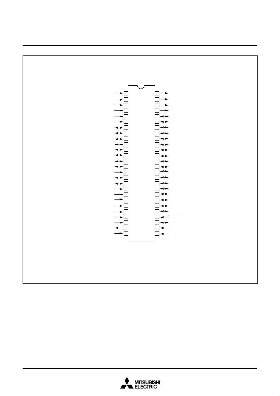
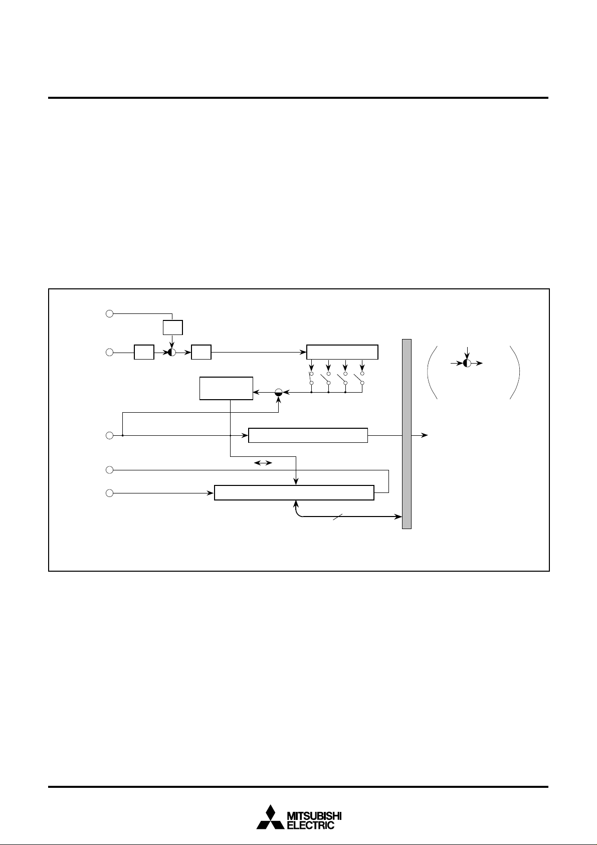
PIN CONFIGURATION (TOP VIEW)
SYNC
H
V
SYNC
P40/AD4
P4
1
/INT2
P4
2
/TIM2
P4
3
/TIM3
P2
4
/AD3
P2
5
/AD2
P26/AD1
P2
P00/PWM4
P0
1
/PWM5
P0
2
/PWM6
7/SIN
P1
P44/INT1
5/SOUT
P4
P4
6/SCLK
AV
HLF
RVCO
V
HOLD
CV
CNV
X
X
OUT
V
CC
SS
SS
1
2
3
4
5
6
M37271EF-XXXSP, M37271EFSP
7
8
9
10
7
11
12
13
14
15
16
17
18
19
20
21
22
IN
23
IN
24
25
26
52
P52/R
51
P5
3
/G
4
/B
P5
50
P5
5
49
48
47
M37271MF-XXXSP
46
45
44
43
42
41
40
39
38
37
36
35
34
33
32
31
30
29
28
27
/OUT1
P0
4
/PWM0
P0
5
/PWM1
P06/PWM2
P07/PWM3
0
P2
1
P2
P2
2
P2
3
0
/OUT2
P1
1
/SCL1
P1
2
/SCL2
P1
P1
3
/SDA1
P1
4
/SDA2
5
/I1
P1
P1
6
/I2/INT3
P0
3
0
P3
P31
RESET
4
/OSC2/X
P6
P63/OSC1/X
V
CC
COUT
CIN
Outline 52P4B
2
Clock input Clock output
X
IN
X
OUT
Reset input
AV
CC
V
CC
V
SS
CNV
SS
Pins for data slicer
Clock output for OSD/
sub-clock output
Input ports P6
3
, P6
4
OSC1 OSC2
Clock input for OSD/
sub-clock input
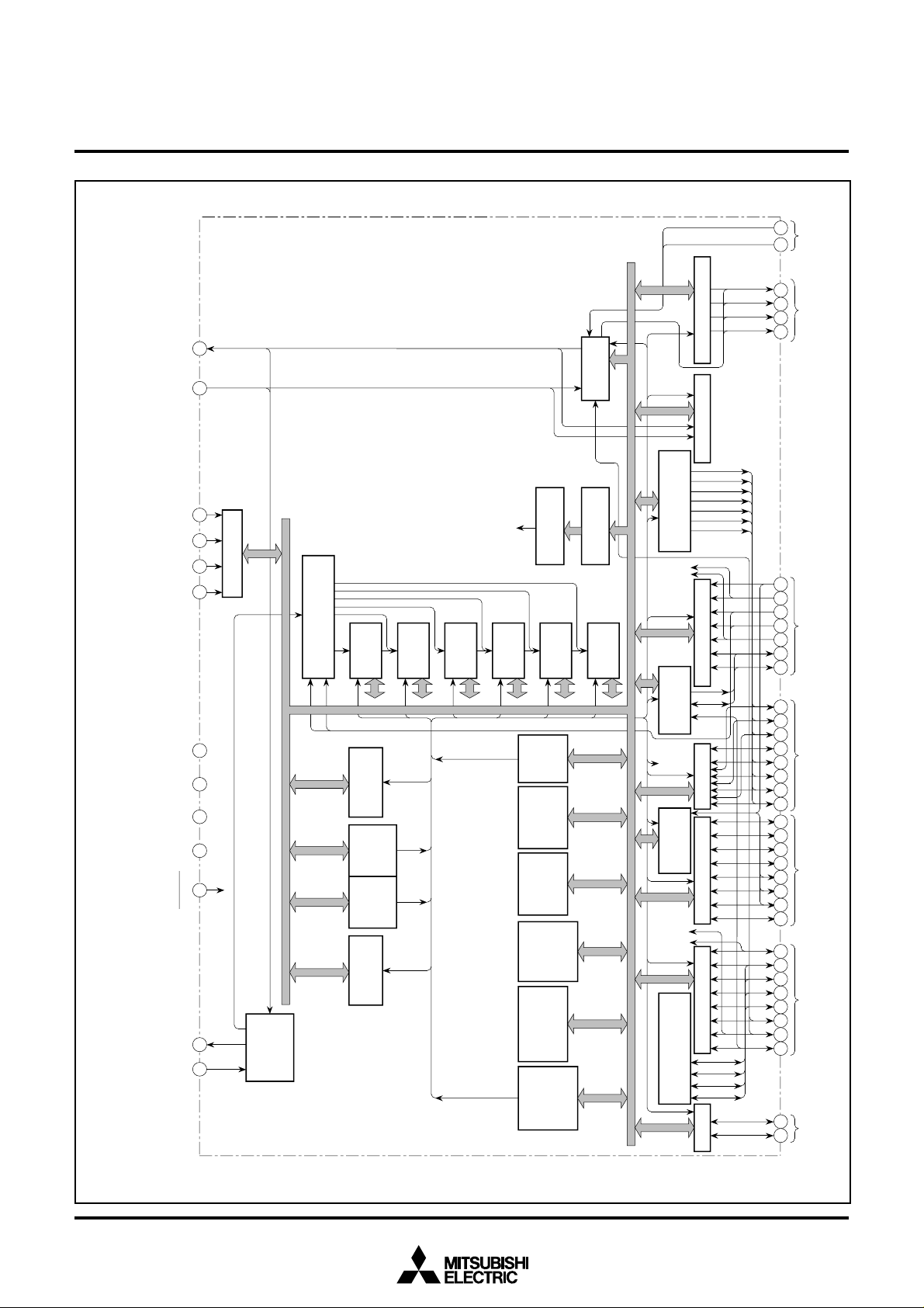
P1 (8)
Multi-master
I
2
C-BUS interface
P3 (2)
SDA1
SCL2
SCL1
SDA2
P2 (8)
P0 (8)
P4 (7)
S
IN
S
CLK
S
OUT
SI/O (8)
P6 (2)
INT1
INT2
PWM6
PWM5
PWM4
PWM3
PWM2
PWM1
PWM0
P5 (4)
OUT1
B
G
R
H
SYNC
V
SYNC
OUT2
A-D
converter
8-bit
PWM circuit
8-bit
arithmetic
and
logical unit
Accumulator
A (8)
Timer 6
T6 (8)
Timer 5
T5 (8)
Timer 4
T4 (8)
Timer 3
T3 (8)
Timer 2
T2 (8)
Timer 1
T1 (8)
Timer count source
selection circuit
TIM2
TIM3
Data slicer
Instruction
register (8)
Instruction
decoder
Control signal
CRT circuit
Processor
status
register
PS (8)
Stack
pointer
S (8)
Index
register
Y (8)
Index
register
X (8)
ROM
60 K bytes
Program
counter
PC
L
(8)
Progam
counter
PC
H
(8)
RAM
1024 bytes
Data bus
Clock
generating
circuit
24 25
30
RESET
18 27 26 23
CV
IN
22 21 20 19
V
HOLD
RVCO
HLF
28 29
Address bus
31 14 34 35 36 37 38 39 40 10 9 8 7 41 42 43 44 45 46 47 48 33 13 12 11 17 16 15 6 5 4 3 49 50 51 52 2 1
I/O ports
P3
0
, P3
1
I/O port P1 I/O port P2 I/O port P0 Input ports P4
0
–P4
6
Output port P5
Sync
signal input
INT3
32
MITSUBISHI MICROCOMPUTERS
M37271MF-XXXSP
M37271EF-XXXSP, M37271EFSP
SINGLE-CHIP 8-BIT CMOS MICROCOMPUTER with CLOSED CAPTION DECODER
and ON-SCREEN DISPLAY CONTROLLER
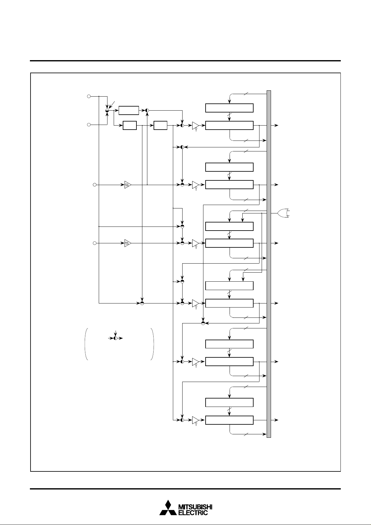
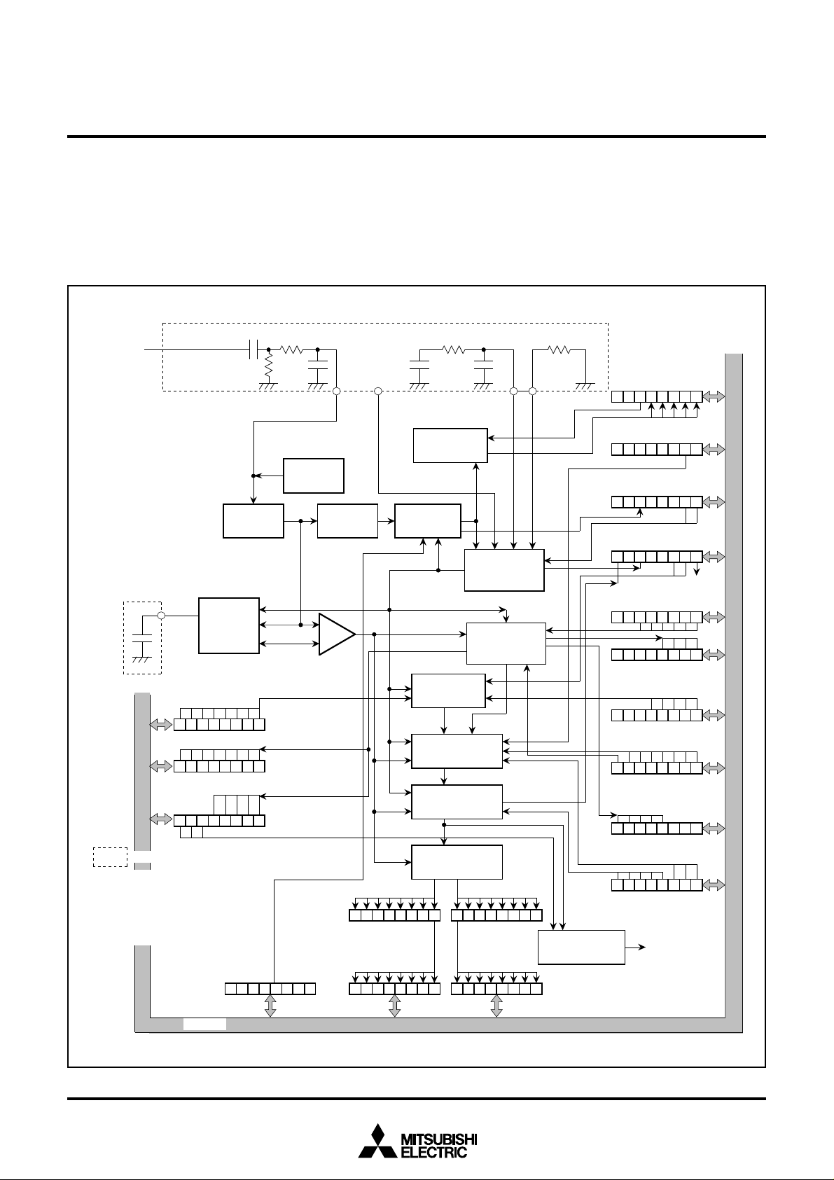
FUNCTIONAL BLOCK DIAGRAM of M37271MF-XXXSP
3
MITSUBISHI MICROCOMPUTERS
M37271MF-XXXSP
M37271EF-XXXSP, M37271EFSP
SINGLE-CHIP 8-BIT CMOS MICROCOMPUTER with CLOSED CAPTION DECODER
and ON-SCREEN DISPLAY CONTROLLER
FUNCTIONS
Parameter
Number of basic instructions
Instruction execution time
Clock frequency
Memory size
Input/Output ports
Serial I/O
Multi-master I2C-BUS interface
A-D converter
PWM output circuit
Timers
Subroutine nesting
Interrupt interval determination circuit
Interrupt
Clock generating circuit
Data slicer
ROM
RAM
OSD ROM
OSD RAM
P00–P02,
P04–P07
P03
P10, P15–P17
P11–P14
P2
P30, P31
P40–P44
P45, P46
P52–P55
P63
P64
I/O
I/O
I/O
I/O
I/O
I/O
Input
Input
Output
Input
Input
71
0.5 µs (the minimum instruction execution time, at 8 MHz oscillation frequency)
8 MHz (maximum)
60 K bytes
1024 bytes
14464 bytes
1920 bytes
7-bit ✕ 1 (N-channel open-drain output structure, can be used as PWM
output pins)
1-bit ✕ 1 (CMOS input/output structure)
4-bit ✕ 1 (CMOS input/output structure, can be used as OSD output pin,
INT input pin, serial input pin)
4-bit ✕ 1 (N-channel open-drain output structure, can be used as multi-
master I2C-BUS interface)
8-bit ✕ 1 (CMOS input/output structure, can be used as A-D input pins)
2-bit ✕ 1 (CMOS input/output structure)
5-bit ✕ 1 (can be used as A-D input pins, INT input pins, external clock
input pins)
2-bit ✕ 1 (N-channel open-drain output structure when serial I/O is used,
can be used as serial I/O pins)
4-bit ✕ 1 (CMOS output structure, can be used as OSD output)
1-bit ✕ 1 (can be used as sub-clock input pin, OSD clock input pin)
1-bit ✕ 1 (CMOS output structure when LC is oscillating, can be used as
sub-clock output pin, OSD clock output pin)
8-bit ✕ 1
1
4 channels (8-bit resolution)
8-bit ✕ 7
8-bit timer ✕ 6
128 levels (maximum)
1
External interrupt ✕ 3, Internal timer interrupt ✕ 6, Serial I/O interrupt ✕ 1,
OSD interrupt ✕ 1, Multi-master I2C-BUS interface interrupt ✕ 1,
Data slicer interrupt ✕ 1, f(XIN)/4092 interrupt ✕ 1, VSYNC interrupt ✕ 1, AD conversion interrupt ✕ 1, BRK instruction interrupt ✕ 1
2 built-in circuits (externally connected a ceramic resonator or a quartzcrystal oscillator)
Built in
Functions
4
MITSUBISHI MICROCOMPUTERS
M37271MF-XXXSP
M37271EF-XXXSP, M37271EFSP
SINGLE-CHIP 8-BIT CMOS MICROCOMPUTER with CLOSED CAPTION DECODER
FUNCTIONS (continued)
and ON-SCREEN DISPLAY CONTROLLER
OSD function
Power source voltage
Power dissipation
Operating temperature range
Device structure
Package
In high-speed
mode
In low-speed
mode
In stop mode
Number of display characters
Dot structure
Kinds of characters
Kinds of character sizes
Kinds of character colors
Display position (horizontal, vertical)
OSD ON
OSD OFF
OSD OFF
Data slicer ON
Data slicer OFF
Data slicer OFF
40 characters ✕ 16 lines
CC mode: 16 ✕ 26 dots (character part : 16 ✕ 20 dots)
OSD mode: 16 ✕ 20 dots
EXOSD mode: 16 ✕ 26 dots
320 kinds
(In EXOSDmode, they can be combined with 32 kinds of extra fonts)
CC mode: 2 kinds
OSD mode: 14 kinds
EXOSD mode: 6 kinds
CC mode: 7 kinds (R, G, B)
OSD mode: 15 kinds (R, G, B, I1)
EXOSD mode: 7 kinds (R, G, B, I1, I2)
256 levels (horizontal) ✕ 1024 levels (vertical)
5 V ± 10 %
165 mW typ. (at oscillation frequency fCPU = 8 MHz, fOSD = 13 MHz)
82.5 mW typ. (at oscillation frequency fCPU = 8 MHz)
0.33mW typ. (at oscillation frequency fCLK = 32 kHz, f(XIN) = stopped)
0.055 mW (maximum)
–10 °C to 70 °C
CMOS silicon gate process
52-pin shrink plastic molded DIP
5
MITSUBISHI MICROCOMPUTERS
M37271MF-XXXSP
M37271EF-XXXSP, M37271EFSP
SINGLE-CHIP 8-BIT CMOS MICROCOMPUTER with CLOSED CAPTION DECODER
and ON-SCREEN DISPLAY CONTROLLER
PIN DESCRIPTION
Pin Name Name
VCC,
AVCC,
VSS.
CNVSS
_____
RESET
XIN
XOUT
P00/PWM4–
P02/PWM6,
P03,
P04/PWM0–
P07/PWM3
P10/OUT2,
P11/SCL1,
P12/SCL2,
P13/SDA1,
P14/SDA2,
P15/I1,
P16/I2/INT3,
P17/SIN
P20–P23
P24/AD3–
P26/AD1,
P27
Power source
CNVSS
Reset input
Clock input
Clock output
I/O port P0
PWM output
I/O port P1
OSD output
Multi-master
I2C-BUS interface
Serial I/O data
input
I/O port P2
Analog input
Input/
Output
Input
Input
Output
I/O
Output
I/O
Output
Output
Input
I/O
Input
Apply voltage of 5 V ± 10 % (typical) to VCC and AVCC, and 0 V to VSS.
This is connected to VSS.
To enter the reset state, the reset input pin must be kept at a “L” for 2 µs or more (under
normal VCC conditions).
If more time is needed for the quartz-crystal oscillator to stabilize, this “L” condition should
be maintained for the required time.
This chip has an internal clock generating circuit. To control generating frequency, an
external ceramic resonator or a quartz-crystal oscillator is connected between pins XIN and
XOUT. If an external clock is used, the clock source should be connected to the XIN pin and
the XOUT pin should be left open.
Port P0 is an 8-bit I/O port with direction register allowing each I/O bit to be individually
programmed as input or output. At reset, this port is set to input mode. The output structure
of P03 is CMOS output, that of P00–P02 and P04–P07 are N-channel open-drain output.
The note out of this Table gives a full of port P0 function.
Pins P00–P02 and P04–P07 are also used as PWM output pins PWM4–PWM6 and PWM0–
PWM3 respectively. The output structure is N-channel open-drain output.
Port P1 is an 8-bit I/O port and has basically the same functions as port P0. The output
structure of P10 and P15–P17 is CMOS output, that of P11–P14 is N-channel open-drain
output.
Pins P10, P15, P16 are also used as OSD output pins OUT2, I1, I2 respectively. The output
structure is CMOS output.
Pins P11–P14 are used as SCL1, SCL2, SDA1 and SDA2 respectively, when multi-master
I2C-BUS interface is used. The output structure is N-channel open-drain output.
P17 pin is also used as serial I/O data input pin SIN.
Port P2 is an 8-bit I/O port and has basically the same functions as port P0. The output
structure is CMOS output.
Pins P24–P26 are also used as analog input pins AD3–AD1 respectively.
P30, P31
P40/AD4,
P41/INT2,
P42/TIM2,
P43/TIM3,
P44/INT1,
P45/SOUT,
P46/SCLK,
P52/R,P53/G,
P54/B,
P55/OUT1
I/O port P3
Input port P4
Analog input
External interrupt
input
External clock input
Serial I/O data
output
Serial I/O
synchronizing clock
input/output
Output port P5
OSD output
I/O
Input
Input
Input
Input
Output
I/O
Output
Output
Ports P30 and P31 are a 2-bit I/O port and has basically the same functions as port P0. The
output structure is CMOS output.
Ports P40–P46 are a 7-bit input port.
P40 pin is also used as analog input pin AD4.
Pins P41, P44 are also used as external interrupt input INT2, INT1.
Pins P42 and P43 are also used as external clock input pins TIM2, TIM3 respectively.
P45 pin is used as serial I/O data output pin SOUT. The output structure is N-channel open-
drain output.
P46 pin is used as serial I/O synchronizing clock input/output pin SCLK. The output struc-
ture is N-channel open-drain output.
Ports P52–P55 are a 4-bit output port. The output structure is CMOS output.
Pins P52–P55 are also used as OSD output pins R, G, B, OUT1 respectively.
6
MITSUBISHI MICROCOMPUTERS
M37271MF-XXXSP
M37271EF-XXXSP, M37271EFSP
SINGLE-CHIP 8-BIT CMOS MICROCOMPUTER with CLOSED CAPTION DECODER
PIN DESCRIPTION (continued)
P63/OSC1/
XCIN,
P64/OSC2/
XCOUT
CVIN
VHOLD
RVCO
HLF
HSYNC
VSYNC
Note : As shown in the memory map (Figure 3), port P0 is accessed as a memory at address 00C016 of zero page. Port P0 has the port P0
Input port
Clock input for OSD
Clock output for OSD
Sub-clock output
Sub-clock input
I/O for data slicer
HSYNC input
VSYNC input
direction register (address 00C116 of zero page) which can be used to program each bit as an input (“0”) or an output (“1”). The pins
programmed as “1” in the direction register are output pins. When pins are programmed as “0,” they are input pins. When pins are
programmed as output pins, the output data are written into the port latch and then output. When data is read from the output pins, the
output pin level is not read but the data of the port latch is read. This allows a previously-output value to be read correctly even if the
output “L” voltage has risen, for example, because a light emitting diode was directly driven. The input pins are in the floating state, so the
values of the pins can be read. When data is written into the input pin, it is written only into the port latch, while the pin remains in the
floating state.
Input
Input
Output
Output
Input
Input
Input
Input
Input
Ports P63 and P64 are 2-bit input port.
P63 pin is also used as OSD clock input pin OSC1.
P64 pin is also used as OSD clock output pin OSC2. The output structure is CMOS output.
P64 pin is also used as sub-clock output pin XCOUT. The output structure is CMOS output.
P63 pin is also used as sub-clock input pin XCIN.
Input composite video signal through a capacitor.
Connect a capacitor between VHOLD and VSS.
Connect a resistor between RVCO and VSS.
Connect a filter using of a capacitor and a resistor between HLF and VSS.
This is a horizontal synchronizing signal input for OSD.
This is a vertical synchronizing signal input for OSD.
and ON-SCREEN DISPLAY CONTROLLER
7
MITSUBISHI MICROCOMPUTERS
M37271MF-XXXSP
M37271EF-XXXSP, M37271EFSP
SINGLE-CHIP 8-BIT CMOS MICROCOMPUTER with CLOSED CAPTION DECODER
and ON-SCREEN DISPLAY CONTROLLER
FUNCTIONAL DESCRIPTION
Central Processing Unit (CPU)
The M37271MF-XXXSP uses the standard 740 family instruction set.
Refer to the table of 740 family addressing modes and machine instructions or the SERIES 740 < Software > User’s Manual for details
on the instruction set.
Machine-resident 740 family instructions are as follows:
The FST, SLW instruction cannot be used.
The MUL, DIV, WIT and STP instruction can be used.
70
11 00
CPU mode register
(CPUM (CM) : address 00FB
Processor mode bits
b1 b0
0 0 : Single-chip mode
0 1 :
1 0 :
1 1 :
Stack page selection bit (Note)
0 : Zero page
1 : 1 page
Fix these bits to “1.”
COUT drivability selection bit
X
0 : Low drive
1 : High drive
Main colock (X
0 : Oscillating
1 : Stopped
Internal system clock selection bit
0 : X
1 : X
CPU Mode Register
The CPU mode register contains the stack page selection bit and
internal system clock selection bit. The CPU mode register is allocated at address 00FB16.
16)
Not available
IN–XOUT) stop bit
IN–XOUT selected (high-speed mode)
CIN–XCOUT selected (low-speed mode)
Note: Please beware of this bit when programming because it
Fig. 1. Structure of CPU mode register
is set to “1” after the reset release.
8
MITSUBISHI MICROCOMPUTERS
M37271MF-XXXSP
M37271EF-XXXSP, M37271EFSP
SINGLE-CHIP 8-BIT CMOS MICROCOMPUTER with CLOSED CAPTION DECODER
and ON-SCREEN DISPLAY CONTROLLER
MEMORY
Special Function Register (SFR) Area
The special function register (SFR) area in the zero page contains
control registers such as I/O ports and timers.
RAM
RAM is used for data storage and for stack area of subroutine calls
and interrupts.
ROM
ROM is used for storing user programs as well as the interrupt vector
area.
RAM for OSD
RAM for display is used for specifying the character codes and colors to display.
ROM for OSD
ROM for display is used for storing character data.
0000
16
Zero page
RAM
(1024 bytes)
RAM for OSD (Note)
(1920 bytes)
00C0
00FF
0200
023F
0300
053F
0800
0FFF
1000
16
16
16
16
16
16
16
16
16
SFR1 area
SFR2 area
Not used
Not used
Interrupt Vector Area
The interrupt vector area contains reset and interrupt vectors.
Zero Page
The 256 bytes from addresses 000016 to 00FF16 are called the zero
page area. The internal RAM and the special function registers (SFR)
are allocated to this area.
The zero page addressing mode can be used to specify memory and
register addresses in the zero page area. Access to this area with
only 2 bytes is possible in the zero page addressing mode.
Special Page
The 256 bytes from addresses FF0016 to FFFF16 are called the special page area. The special page addressing mode can be used to
specify memory addresses in the special page area. Access to this
area with only 2 bytes is possible in the special page addressing
mode.
10000
ROM for OSD
(14464 bytes)
10800
1567F
18000
16
16
16
16
Not used
Not used
ROM
(60 K bytes)
Fig. 2. Memory map
FF00
FFDE
FFFF
16
16
Interrupt vector area
16
Special page
1E43F
1FFFF
16
16
Not used
9
MITSUBISHI MICROCOMPUTERS
M37271MF-XXXSP
M37271EF-XXXSP, M37271EFSP
SINGLE-CHIP 8-BIT CMOS MICROCOMPUTER with CLOSED CAPTION DECODER
and ON-SCREEN DISPLAY CONTROLLER
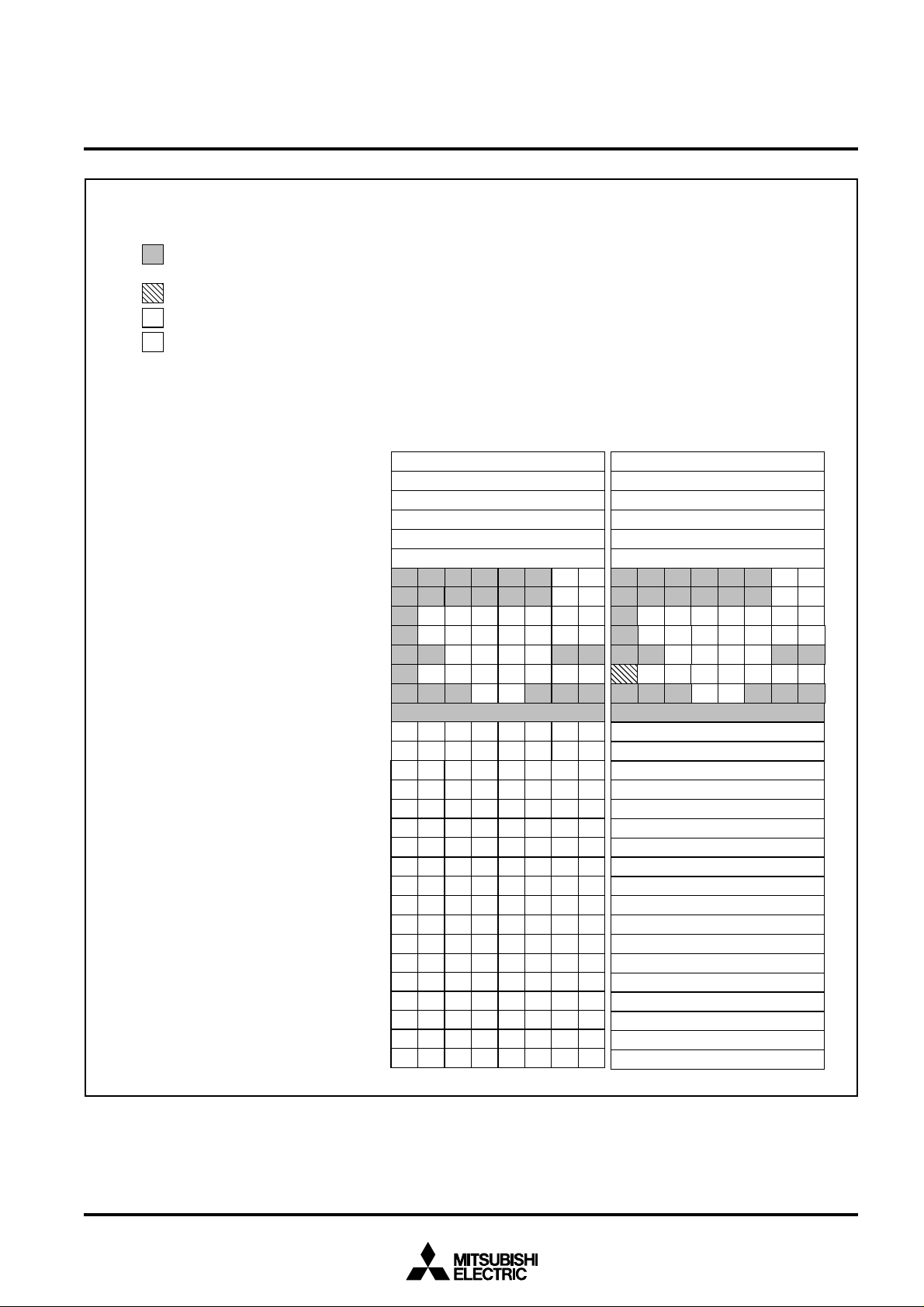
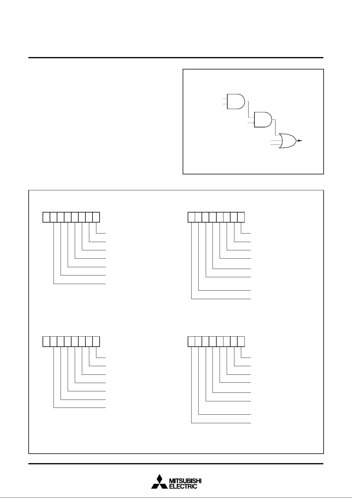
■SFR1 area (addresses C016 to DF16)
: Nothing is allocated
: Fix this bit to “0” ( do not write “1”)
: “0” immediately after reset
0
?
: undefined immediately after reset
Address
C0
16
C1
16
C2
16
C3
16
C4
16
C5
16
C6
16
C7
16
C8
16
C9
16
CA
16
CB
16
CC
16
CD
16
CE
16
CF
16
D0
16
D1
16
D2
16
D3
16
D4
16
D5
16
D6
16
D7
16
D8
16
D9
16
DA
16
DB
16
DC
16
DD
16
DE
16
DF
16
Register
Port P0 (P0)
Port P0 direction register (D0)
Port P1 (P1)
Port P1 direction register (D1)
Port P2 (P2)
Port P2 direction register (D2)
Port P3 (P3)
Port P3 direction register (D3)
Port P4 (P4)
Port P4 direction register (D4)
Port P5 (P5)
OSD port control register (PF)
Port P6 (P6)
OSD control register (OC)
Horizontal position register (HP)
Block control register 1 (BC1)
Block control register 2 (BC2)
Block control register 3 (BC3)
Block control register 4 (BC4)
Block control register 5 (BC5)
Block control register 6 (BC6)
Block control register 7 (BC7)
Block control register 8 (BC8)
Block control register 9 (BC9)
Block control register 10 (BC10)
Block control register 11 (BC11)
Block control register 12 (BC12)
Block control register 13 (BC13)
Block control register 14 (BC14)
Block control register 15 (BC15)
Block control register 16 (BC16)
b7
Bit allocation State immediately after reset
OUT1OUT2
OC6OC7 OC4OC5 OC2OC3 OC0OC1
HP6HP7 HP4HP5 HP2HP3 HP0HP1
b0
b7
b0
?
16
00
?
16
00
?
16
00
???
?????
00000000
????????
0000000
???????
RI2I1GB
00000000
0
?
????????
?
00
16
00
16
BC11BC12BC13BC14BC15BC16BC17BC18
BC21BC22BC23BC24BC25BC26BC27BC28
BC31BC32BC33BC34BC35BC36BC37BC38
BC41BC42BC43BC44BC45BC46BC47BC48
BC51BC52BC53BC54BC55BC56BC57BC58
BC61BC62BC63BC64BC65BC66BC67BC68
BC71BC72BC73BC74BC75BC76BC77BC78
BC81BC82BC83BC84BC85BC86BC87BC88
BC91BC92BC93BC94BC95BC96BC97BC98
BC101BC102BC103BC104BC105BC106BC107BC108
BC111BC112BC113BC114BC115BC116BC117BC118
BC121BC122BC123BC124BC125BC126BC127BC128
BC131BC132BC133BC134BC135BC136BC137BC138
BC141BC142BC143BC144BC145BC146BC147BC148
BC151BC152BC153BC154BC155BC156BC157BC158
BC161BC162BC163BC164BC165BC166BC167BC168
?
?
?
?
?
?
?
?
?
?
?
?
?
?
?
?
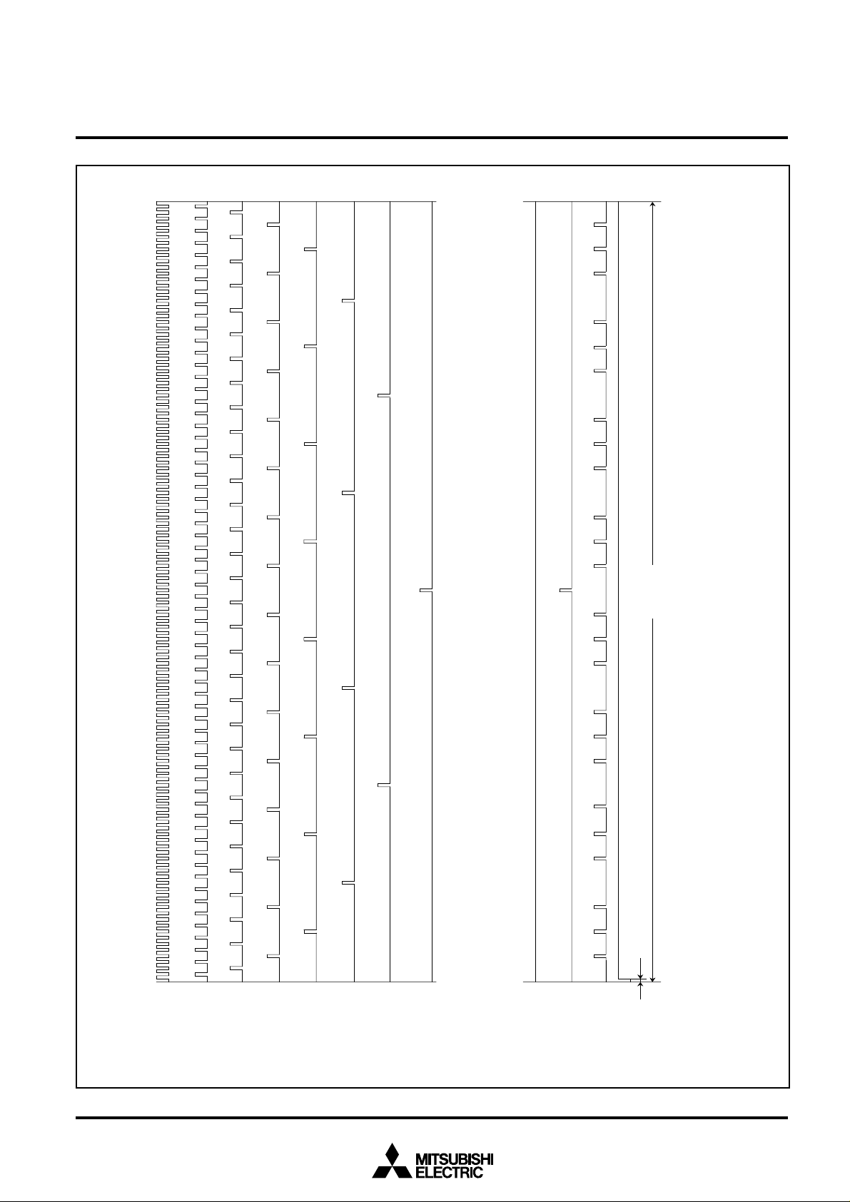
Fig. 3. Memory map of special function register 1 (SFR1) (1)
10
SINGLE-CHIP 8-BIT CMOS MICROCOMPUTER with CLOSED CAPTION DECODER
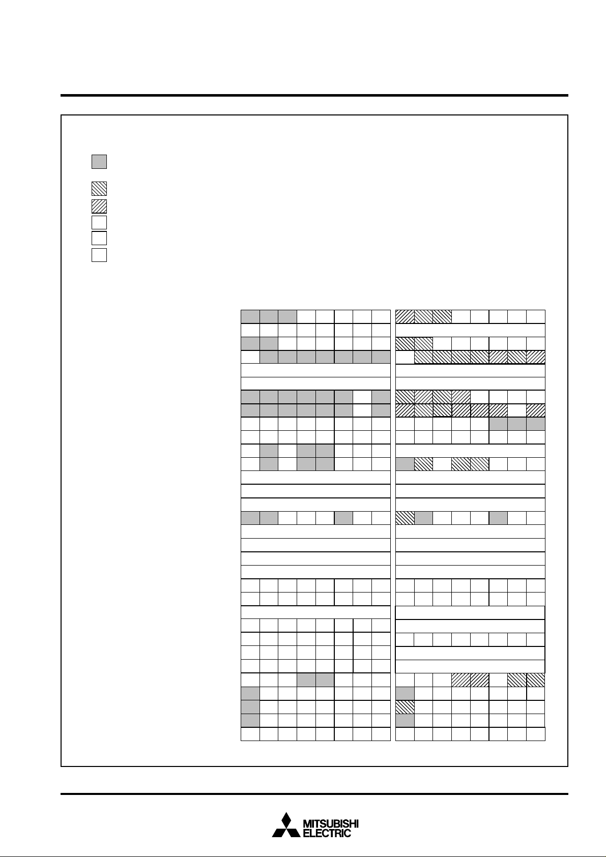
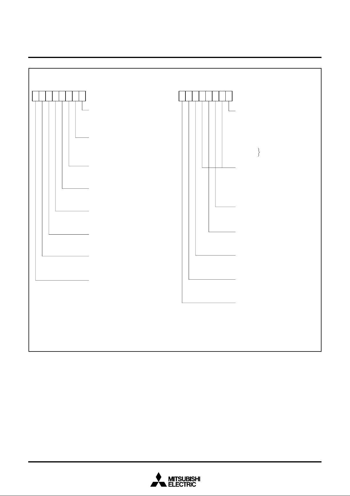
■SFR1 area (addresses E016 to FF16)
: Nothing is allocated
: Fix this bit to “0” ( do not write “1”)
: Fix this bit to “1” ( do not write “0”)
: “0” immediately after reset
0
: “1” immediately after reset
1
?
: undefined immediately after reset
MITSUBISHI MICROCOMPUTERS
M37271MF-XXXSP
M37271EF-XXXSP, M37271EFSP
and ON-SCREEN DISPLAY CONTROLLER
Address Register
Caption position register (CP)
E0
16
Start bit position register (SP)
E1
16
E2
16
Window register (WN)
E3
16
Sync slice register (SSL)
E4
16
Data register 1 (CD1)
E5
16
Data register 2 (CD2)
E6
16
Clock run-in register 1 (CR1)
Clock run-in register 2 (CR2)
E7
16
Clock run-in detect register 1 (CRD1)
E8
16
Clock run-in detect register 2 (CRD2)
E9
16
Data slicer control register 1 (DSC1)
EA
16
Data slicer control register 2 (DSC2)
EB
16
EC
16
Data register 3 (CD3)
Data register 4 (CD4)
ED
16
A-D conversion register (AD)
EE
16
EF
16
A-D control register (ADCON)
F0
16
Timer 1 (TM1)
Timer 2 (TM2)
F1
16
F2
16
Timer 3 (TM3)
F3
16
Timer 4 (TM4)
F4
16
Timer mode register 1 (TM1)
F5
16
Timer mode register 2 (TM2)
I2C
F6
F7
F8
F9
FA
FB
FC
FD
FE
FF
data shift register (S0)
16
16
I2C
address register (S0D)
I2C
status register (S1)
16
I2C
control register (S1D)
16
I2C
clock control register (S2)
16
16
CPU mode
16
Interrupt request
16
Interrupt request
Interrupt control
16
16
Interrupt control
register (CPUM)
register 1 (ICON1)
register 2 (ICON2)
b7
register 1 (IREQ1)
register 2 (IREQ2)
SSL7
ACK
Bit allocation State immediately after reset
b0
b7
1 00?? ?? ?
CP0CP1CP2CP3CP4
00
SP0SP1SP2SP3SP4SP5SP6SP7
0 0000 00 0
WN0WN1WN2WN3WN4WN5
16
0 0000 01 1
?
?
CR11
CR21
0 1010000
1 00111 10
CRD10CRD11CRD12CRD15CRD17CRD15 CRD15CRD15
000 00 00 0
CRD20CRD21CRD22CRD25CRD27CRD25 CRD25CRD25
000 01 00 1
DSC10DSC11DSC12DSC15DSC17
DSC20DSC21DSC22DSC25DSC27
? 0000 00 0
0
00
00
?
16
16
?
ADVREF
ADV
TM15TM16TM17
TM25
TM26TM27
ADSTR
ADIN0ADIN1
TM10TM11TM12TM13TM14
TM20TM21TM22TM23TM24
?000?000
16
FF
07
16
FF
16
07
16
00000000
00000000
?
BSEL0BSEL1
ACK
BIT
ADE
10 BIT
SAD
FAST
MODE
IICRT56R
IICET56ET56S
INT2R
CK0
1MSR
1MSE
CM2
SAD0SAD1SAD2SAD3SAD4SAD5SAD6 RBW
LRBAD0AASALPINBBTRXMST
BC0BC1BC2ES0ALS
CCR0CCR1CCR2CCR3CCR4
CM0CM1CM7 CM5CM6
TM1RTM2RTM3RTM4RCRTRVSCRADR
INT1R
DSRSIOR
TM1ETM2ETM3ETM4ECRTEVSCE
INT1EDSESIOEINT2E
0
0111 00
0000 0000
0000 00
00
0000 0000
0000 0000
00
16
000001?0
00
16
00
16
CK0
b0
1
Fig. 4. Memory map of special function register 1 (SFR2) (2)
11
MITSUBISHI MICROCOMPUTERS
M37271MF-XXXSP
M37271EF-XXXSP, M37271EFSP
SINGLE-CHIP 8-BIT CMOS MICROCOMPUTER with CLOSED CAPTION DECODER
and ON-SCREEN DISPLAY CONTROLLER
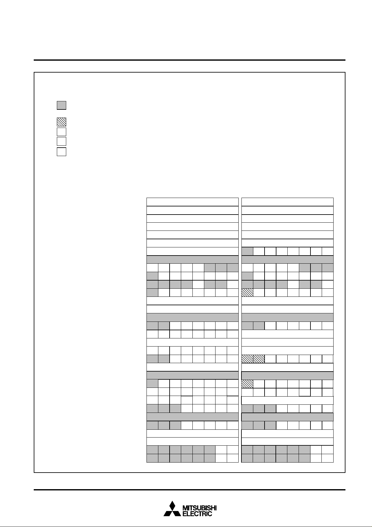
■SFR2 area (addresses 20016 to 21F16)
: Nothing is allocated
: Fix this bit to “0” ( do not write “1”)
: “0” immediately after reset
0
: “1” immediately after reset
1
?
: undefined immediately after reset
Address Register
200
201
202
203
204
205
206
207
208
209
20A
20B
20C
20D
20E
20F
210
211
212
213
214
215
216
217
218
219
21A
21B
21C
21D
21E
21F
PWM0 register (PWM0)
16
16
PWM1 register (PWM1)
16
PWM2 register (PWM2)
16
PWM3 register (PWM3)
16
PWM4 register (PWM4)
16
PWM5 register (PWM5)
16
PWM6 register (PWM6)
16
Clock run-in detect register (CRD3)
16
16
Clock run-in register (CR3)
16
PWM mode register 1 (PN)
16
PWM mode register 2 (PW)
16
Timer 5 (TM5)
Timer 6 (TM6)
16
16
Sync pulse counter register (SYC)
16
Data slicer control register 3 (DSC3)
16
Interrupt interval determination register (RI)
16
Interrupt interval determination control register (RE)
16
Serial I/O mode register (SM)
16
Serial I/O register (SIO)
16
16
16
Clock source control register (CS)
16
I/O polarity control register (PC)
16
Raster color register (RC)
Extra font color register (EC)
16
16
16
Border color register (FC)
Window H register 1 (WH1)
16
16
Window L register 1 (WH1)
Window H register 2 (WH2)
16
Window L register 2 (WH2)
16
b7
Bit allocation State immediately after reset
DSC36 DSC34DSC33
INT3
INT3
AD/INT3
AD/INT3
SEL
SEL
POL
POL
INT3
AD/INT3
SEL
POL
INT3
AD/INT3
SEL
POL
INT3
AD/INT3
SEL
POL
INT3
AD/INT3
SEL
POL
INT3
AD/INT3
SEL
POL
CRD31CRD32CRD33CRD34CRD35
POL
FC2
b0
b7
b0
?
?
?
?
?
?
? 0000 00 0
?
0 0000 00 0
??? ?? ?? ?
ENABLE
? ???0 ?? 0
0 ???? ?? ?
PW0PW1PW2PW3PW4PW5PW6
07
16
FF
16
?
SYC0
SYC1SYC2SYC3SYC4SYC5
DSC30DSC31DSC32DSC37 DSC35
?000000?
00
16
?
00
RE0RE1RE2RE3RE4RE5
RE1RE2RE3RE4RE5
SM0RE1RE2RE3SM4RE5
SM1SM2SM3SM5
16
000000 00
?
?
RE1RE2RE3RE5
CS0CS4 CS1CS2CS3CS5CS6
PC0RE1RE2RE3PC4RE5
PC1PC2PC3PC5PC6PC7
RC0RE1RE2RE3RC4RE5
RC1RC2RC3RC5RC6RC7
RE1RE2RE3RE5
00
?0 ???? ??
010000 00
16
0? ? ?00 00
?
FC0FC1FC3FC4
0? ? ?00 00
?
?
WH20WH21
???
WL20WL21
??????
?????
??
Fig. 5. Memory map of special function register 2 (SFR2) (1)
12
MITSUBISHI MICROCOMPUTERS
M37271MF-XXXSP
M37271EF-XXXSP, M37271EFSP
SINGLE-CHIP 8-BIT CMOS MICROCOMPUTER with CLOSED CAPTION DECODER
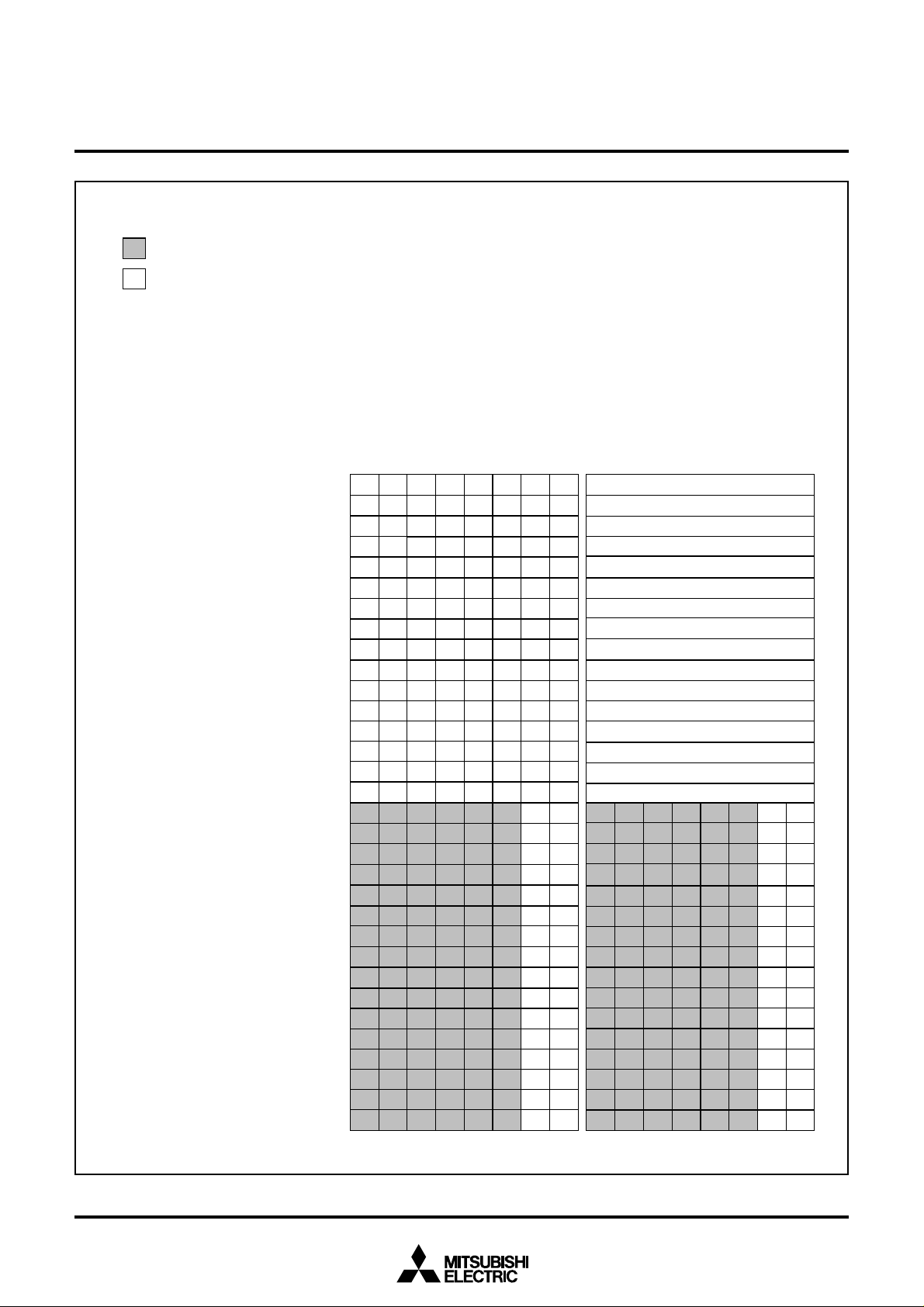
■SFR2 area (addresses 22016 to 23F16)
: Nothing is allocated
?
: undefined immediately after reset
and ON-SCREEN DISPLAY CONTROLLER
Address Register
220
221
222
223
224
225
226
227
228
229
22A
22B
22C
22D
22E
22F
230
231
232
233
234
235
236
237
238
239
23A
23B
23C
23D
23E
23F
Vertical position register 1
16
Vertical position register 1
16
Vertical position register 1
16
Vertical position register 14 (VP14)
16
Vertical position register 1
16
Vertical position register 1
16
Vertical position register 1
16
Vertical position register 18 (VP18)
16
Vertical position register 1
16
Vertical position register 1
16
Vertical position register 1
16
Vertical position register 1
16
Vertical position register 1
16
Vertical position register 1
16
Vertical position register 1
16
Vertical position register 1
16
Vertical position register 2
16
Vertical position register 2
16
Vertical position register 2
16
Vertical position register 2
16
16
Vertical position register 2
16
Vertical position register 2
Vertical position register 27 (VP27)
16
16
Vertical position register 2
Vertical position register 2
16
Vertical position register 2
16
Vertical position register 2
16
Vertical position register 2
16
Vertical position register 2
16
Vertical position register 2
16
16
Vertical position register 2
16
Vertical position register 2
(VP11)
1
(VP12)
2
(VP13)
3
(VP15)
5
(VP16)
6
(VP17)
7
(VP19)
9
(VP110)
10
(VP111)
11
(VP112)
12
(VP113)
13
(VP114)
14
(VP115)
15
(VP116)
16
(VP21)
1
(VP22)
2
(VP23)
3
(VP24)
4
(VP25)
5
(VP26)
6
(VP28)
8
(VP29)
9
(VP210)
10
(VP211)
11
(VP212)
12
(VP213)
13
(VP214)
14
(VP215)
15
(VP216)
16
b7
Bit allocation State immediately after reset
b0
b7
VP111
VP112VP113VP114VP115VP116VP117VP118
VP121VP122VP123VP124VP125VP126VP127VP128
VP131VP132VP133VP134VP135VP136VP137VP138
VP141VP142VP143VP144VP145VP146VP147VP148
VP151VP152VP153VP154VP155VP156VP157VP158
VP161VP162VP163VP164VP165VP166VP167VP168
VP171VP172VP173VP174VP175VP176VP177VP178
VP181VP182VP183VP184VP185VP186VP187VP188
VP191VP192VP193VP194VP195VP196VP197VP198
VP1101VP1102VP1103VP1104VP1105VP1106VP1107VP1108
VP1111VP1112VP1113VP1114VP1115VP1116VP1117VP1118
VP1121VP1122VP1123VP1124VP1125VP1126VP1127VP1128
VP1131VP1132VP1133VP1134VP1135VP1136VP1137VP1138
VP1141VP1142VP1143VP1144VP1145VP1146VP1147VP1148
VP1151VP1152VP1153VP1154VP1155VP1156VP1157VP1158
VP1161VP1162VP1163VP1164VP1165VP1166VP1167VP1168
VP211VP212
VP221VP222
VP231VP232
VP241VP242
VP251VP252
VP261VP262
VP271VP272
VP281VP282
VP291VP292
VP2101VP2102
VP2111VP2112
VP2121VP2122
VP2131VP2132
VP2141VP2142
VP2151VP2152
VP2161VP2162
?
?
?
?
?
?
?
?
?
?
?
?
?
?
?
?
b0
????????
????????
????????
????????
????????
????????
????????
????????
????????
????????
????????
????????
????????
????????
????????
????????
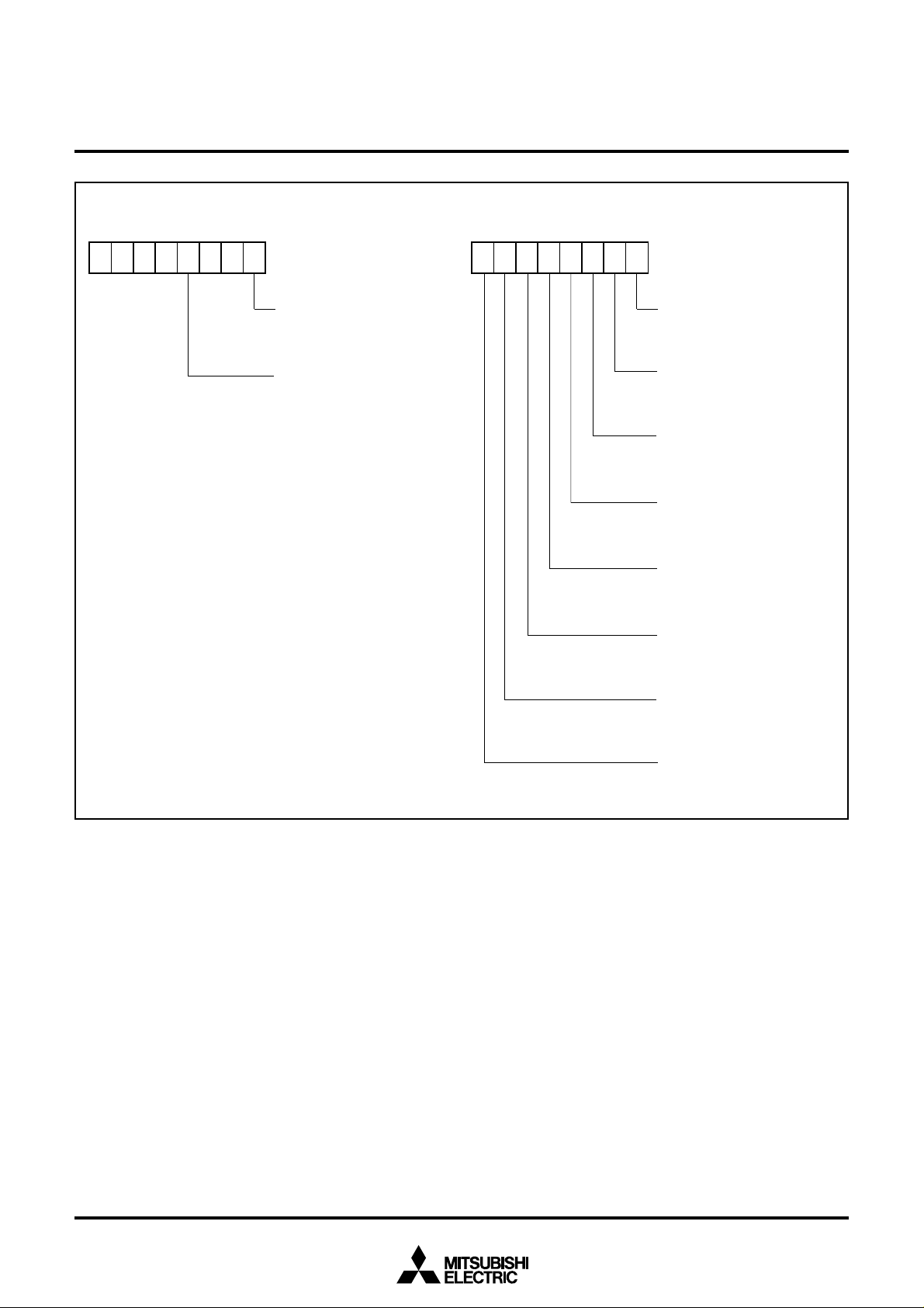
Fig. 6. Memory map of special function register 2 (SFR2) (2)
13
MITSUBISHI MICROCOMPUTERS
M37271MF-XXXSP
M37271EF-XXXSP, M37271EFSP
SINGLE-CHIP 8-BIT CMOS MICROCOMPUTER with CLOSED CAPTION DECODER
and ON-SCREEN DISPLAY CONTROLLER
: Nothing is allocated
1
: “1” immediately after reset
?
: undefined immediately after reset
Register
b7
Processor status register (PS)
Program counter (PCH)
Program counter (PCL)
Fig. 7. Internal state of processor status register and program counter at reset
Bit allocation State immediately after reset
I ZCDBTVN???????
b0
b7
Contents of address FFFF
Contents of address FFFE
b0
1
16
16
14
MITSUBISHI MICROCOMPUTERS
M37271MF-XXXSP
M37271EF-XXXSP, M37271EFSP
SINGLE-CHIP 8-BIT CMOS MICROCOMPUTER with CLOSED CAPTION DECODER
and ON-SCREEN DISPLAY CONTROLLER
INTERRUPTS
Interrupts can be caused by 18 different sources consisting of 4 external, 12 internal, 1 software, and reset. Interrupts are vectored interrupts with priorities shown in Table 1. Reset is also included in the
table because its operation is similar to an interrupt.
When an interrupt is accepted,
(1) The contents of the program counter and processor status
register are automatically stored into the stack.
(2) The interrupt disable flag I is set to “1” and the corresponding
interrupt request bit is set to “0.”
(3) The jump destination address stored in the vector address enters
the program counter.
Other interrupts are disabled when the interrupt disable flag is set to
“1.”
All interrupts except the BRK instruction interrupt have an interrupt
request bit and an interrupt enable bit. The interrupt request bits are
in interrupt request registers 1 and 2 and the interrupt enable bits are
in interrupt control registers 1 and 2. Figure 8 shows the structure of
the interrupt-related registers.
Interrupts other than the BRK instruction interrupt and reset are accepted when the interrupt enable bit is “1,” interrupt request bit is “1,”
and the interrupt disable flag is “0.” The interrupt request bit can be
set to “0” by a program, but not set to “1.” The interrupt enable bit can
be set to “0” and “1” by a program.
Reset is treated as a non-maskable interrupt with the highest priority.
Figure 9 shows interrupt control.
Interrupt Causes
(1) VSYNC and OSD interrupts
The VSYNC interrupt is an interrupt request synchronized with
the vertical sync signal.
The OSD interrupt occurs after character block display to the
CRT is completed.
(2) INT1, INT2, INT3 interrupts
With an external interrupt input, the system detects that the level
of a pin changes from “L” to “H” or from “H” to “L,” and generates
an interrupt request. The input active edge can be selected by
bits 3, 4 and 6 of the interrupt interval determination control register (address 021216) : when this bit is “0,” a change from “L” to
“H” is detected; when it is “1,” a change from “H” to “L” is detected. Note that all bits are cleared to “0” at reset.
(3) Timer 1, 2, 3 and 4 interrupts
An interrupt is generated by an overflow of timer 1, 2, 3 or 4.
(4) Serial I/O interrupt
This is an interrupt request from the clock synchronous serial
I/O function.
(5) f(XIN)/4096 interrupt
This interrupt occurs regularly with a f(XIN)/4096 period. Set bit 0
of the PWM mode register 1 to “0.”
(6) Data slicer interrupt
An interrupt occurs when slicing data is completed.
(7) Multi-master I2C-BUS interface interrupt
This is an interrupt request related to the multi-master I2C-BUS
interface.
(8) A-D conversion interrupt
An interrupt occurs at the completion of A-D conversion. Since
A-D conversion interrupt and the INT3 interrupt share the same
vector, an interrupt source is selected by bit 7 of the interrupt
interval determination control register (address 021216).
Table 1. Interrupt vector addresses and priority
Interrupt source
Reset
OSD interrupt
INT1 interrupt
Data slicer interrupt
Serial I/O interrupt
Timer 4 interrupt
f(XIN)/4096 interrupt
VSYNC interrupt
Timer 3 interrupt
Timer 2 interrupt
Timer 1 interrupt
A-D convertion · INT3 interrupt
INT2 interrupt
Multi-master I2C-BUS interface interrupt
Timer 5 · 6 interrupt
BRK instruction interrupt
Priority
1
2
3
4
5
6
7
8
9
10
11
12
13
14
15
16
Vector addresses
FFFF16, FFFE16
FFFD16, FFFC16
FFFB16, FFFA16
FFF916, FFF816
FFF716, FFF616
FFF516, FFF416
FFF316, FFF216
FFF116, FFF016
FFEF16, FFEE16
FFED16, FFEC16
FFEB16, FFEA16
FFE916, FFE816
FFE716, FFE616
FFE516, FFE416
FFE316, FFE216
FFDF16, FFDE16
Remarks
Non-maskable
Active edge selectable
Active edge selectable
Active edge selectable
Active edge selectable
Non-maskable (software interrupt)
15
MITSUBISHI MICROCOMPUTERS
M37271MF-XXXSP
M37271EF-XXXSP, M37271EFSP
SINGLE-CHIP 8-BIT CMOS MICROCOMPUTER with CLOSED CAPTION DECODER
and ON-SCREEN DISPLAY CONTROLLER
(9)Timer 5 · 6 interrupt
An interrupt is generated by an overflow of timer 5 or 6. Their
priorities are same, and can be switched by software.
(10)BRK instruction interrupt
This software interrupt has the least significant priority. It does
not have a corresponding interrupt enable bit, and it is not affected by the interrupt disable flag I (non-maskable).
Interrupt request bit
Interrupt enable bit
Interrupt disable flag I
BRK instruction
Reset
Interrupt
request
Fig. 9. Interrupt control
7
0
Interrupt request register 1
(IREQ1: address 00FC
Timer 1 interrupt request bit
Timer 2 interrupt request bit
Timer 3 interrupt request bit
Timer 4 interrupt request bit
OSD interrupt request bit
V
SYNC
interrupt request bit
A-D conversion ⋅ INT3 interrupt
request bit
7
16
)
0
0
Interrupt request register 2
(IREQ2: address 00FD
16
)
INT1 interrupt request bit
Data slicer interrupt request bit
Serial I/O interrupt request bit
f(XIN)/4096 interrupt request bit
INT2 interrupt request bit
Multi-master I2C-BUS
interface interrupt request bit
Timer 5 ⋅ 6 interrupt request bit
Fix this bit to “0.”
0 : No interrupt request issued
1 : Interrupt request issued
7
0
Interrupt control register 1
( ICON1: address 00FE
Timer 1 interrupt enable bit
Timer 2 interrupt enable bit
Timer 3 interrupt enable bit
Timer 4 interrupt enable bit
OSD interrupt enable bit
V
SYNC
interrupt enable bit
A-D conversion ⋅ INT3 interrupt
request bit
Fig. 8. Structure of interrupt-related registers
16
7
16
)
0 : Interrupt disabled
1 : Interrupt enabled
0
Interrupt control register 2
( ICON2 : address 00FF
INT1 interrupt enable bit
Data slicer interrupt enable bit
Serial I/O interrupt enable bit
f(XIN)/4096 interrupt enable bit
INT2 interrupt enable bit
2
Multi-master I
C-BUS
interface enable bit
Timer 5 ⋅ 6 interrupt enable bit
Timer 5 ⋅ 6 interrupt switch bit
0 : Timer 5
1 : Timer 6
16
)

MITSUBISHI MICROCOMPUTERS
M37271MF-XXXSP
M37271EF-XXXSP, M37271EFSP
SINGLE-CHIP 8-BIT CMOS MICROCOMPUTER with CLOSED CAPTION DECODER
and ON-SCREEN DISPLAY CONTROLLER
TIMERS
The M37271MF-XXXSP has 6 timers: timer 1, timer 2, timer 3,
timer 4, timer 5, and timer 6. All timers are 8-bit timers with the 8-bit
timer latch. The timer block diagram is shown in Figure 11.
All of the timers count down and their divide ratio is 1/(n+1), where n
is the value of timer latch. The value is set to a timer at the same time
by writing a count value to the corresponding timer latch (addresses
00F016 to 00F316 : timers 1 to 4, addresses 020C16 and 020D16 :
timers 5 and 6).
The count value is decremented by 1. The timer interrupt request bit
is set to “1” by a timer overflow at the next count pulse after the count
value reaches “0016”.
(1) Timer 1
Timer 1 can select one of the following count sources:
f(XIN)/16 or f(XCIN)/16
•
f(XIN)/4096 or f(XCIN)/4096
•
External clock from the P42/TIM2 pin
•
The count source of timer 1 is selected by setting bits 5 and 0 of the
timer mode register 1 (address 00F416). Either f(XIN) or f(XCIN) is
selected by bit 7 of the CPU mode register.
Timer 1 interrupt request occurs at timer 1 overflow.
(2) Timer 2
Timer 2 can select one of the following count sources:
f(XIN)/16 or f(XCIN)/16
•
Timer 1 overflow signal
•
External clock from the P42/TIM2 pin
•
The count source of timer 2 is selected by setting bits 4 and 1 of the
timer mode register 1 (address 00F416). Either f(XIN) or f(XCIN) is
selected by bit 7 of the CPU mode register. When timer 1 overflow
signal is a count source for the timer 2, the timer 1 functions as an 8bit prescaler.
Timer 2 interrupt request occurs at timer 2 overflow.
(3) Timer 3
Timer 3 can select one of the following count sources:
f(XIN)/16 or f(XCIN)/16
•
f(XCIN)
•
External clock from the P43/TIM3 pin
•
The count source of timer 3 is selected by setting bit 0 of the timer
mode register 2 (address 00F516) and bit 6 at address 00C716. Either f(XIN) or f(XCIN) is selected by bit 7 of the CPU mode register.
Timer 3 interrupt request occurs at timer 3 overflow.
(5) Timer 5
Timer 5 can select one of the following count sources:
f(XIN)/16 or f(XCIN)/16
•
Timer 2 overflow signal
•
Timer 4 overflow signal
•
The count source of timer 3 is selected by setting bit 6 of the timer
mode register 1 (address 00F416) and bit 7 of the timer mode register 2 (address 00F516). Either f(XIN) or f(XCIN) is selected by bit 7 of
the CPU mode register.
Timer 5 interrupt request occurs at timer 5 overflow.
(6) Timer 6
Timer 6 can select one of the following count sources:
f(XIN)/16 or f(XCIN)/16
•
Timer 5 overflow signal
•
The count source of timer 6 is selected by setting bit 7 of the timer
mode register 1 (address 00F416). Either f(XIN) or f(XCIN) is selected
by bit 7 of the CPU mode register. When timer 5 overflow signal is a
count source for the timer 6, the timer 5 functions as an 8-bit prescaler.
Timer 6 interrupt request occurs at timer 6 overflow.
At reset, timers 3 and 4 are connected by hardware and “FF16” is
automatically set in timer 3; “0716” in timer 4. The f(XIN) ✽ /16 is selected as the timer 3 count source. The internal reset is released by
timer 4 overflow at these state, the internal clock is connected.
At execution of the STP instruction, timers 3 and 4 are connected by
hardware and “FF16” is automatically set in timer 3; “0716” in timer 4.
However, the f(XIN) ✽ /16 is not selected as the timer 3 count source.
So set both bit 0 of the timer mode register 2 (address 00F516) and
bit 6 at address 00C716 to “0” before the execution of the STP instruction (f(XIN) ✽ /16 is selected as the timer 3 count source). The
internal STP state is released by timer 4 overflow at these state, the
internal clock is connected.
Because of this, the program starts with the stable clock.
✽ : When bit 7 of the CPU mode register (CM7) is “1,” f(XIN) be-
comes f(XCIN).
The structure of timer-related registers is shown in Figure 10.
(4) Timer 4
Timer 4 can select one of the following count sources:
f(XIN)/16 or f(XCIN)/16
•
f(XIN)/2 or f(XCIN)/2
•
f(XCIN)
•
The count source of timer 3 is selected by setting bits 4 and 1 of the
timer mode register 2 (address 00F516). Either f(XIN) or f(XCIN) is
selected by bit 7 of the CPU mode register. When timer 3 overflow
signal is a count source for the timer 4, the timer 3 functions as an 8bit prescaler.
Timer 4 interrupt request occurs at timer 4 overflow.
17
70
Timer mode register 1
(TMR1 : address 00F416)
Timer 1 count source selection bit 1
0 : f(X
IN
)/16 or f(X
CIN
)/16 (Note)
1 : Count source selected by bit 5
of TMR1
Timer 2 count source selection bit 1
0 : Count source selected by bit 4 of
TMR1
1 : External clock from P42/TIM2 pin
Timer 1 count stop bit
0 : Count start
1 : Count stop
Timer 2 count stop bit
0 : Count start
1 : Count stop
Timer 2 count source selection bit 2
0 : f(XIN)/16 or f(X
CIN
)/16 (Note)
1 : Timer 1 overflow
Timer 1 count source selection bit 2
0 : f(XIN)/4096 or f(X
CIN
)/4096 (Note)
1 : External clock from P42/TIM2
pin
Timer 5 count source selection bit 2
0 : Timer 2 overflow
1 : Timer 4 overflow
Timer 6 count source selection bit
0 : f(XIN)/16 or f(X
CIN
)/16 (Note)
1 : Timer 5 overflow
70
Timer mode register 2
(TMR2 : address 00F5
16
)
Timer 3 count stop bit
0 : Count start
1 : Count stop
Timer 4 count stop bit
0 : Count start
1 : Count stop
Timer 5 count stop bit
0 : Count start
1 : Count stop
Timer 6 count stop bit
0 : Count start
1 : Count stop
Timer 5 count source selection bit 1
0 : f(XIN)/16 or f(X
CIN
)/16 (Note)
1 : Count source selected by bit 6
of TMR1
Timer 3 count source selection bit
0 0 : f(XIN)/16 or f(X
CIN
)/16 (Note)
1 0 : f(X
CIN
)
0 1 :
1 1 :
(Bit 6 at
address
00C7
16
)
External clock from
P43/TIM3 pin
Timer 4 count source selection bits
b4 b1
0 0 : Timer 3 overflow
0 1 : f(XIN)/16 or f(X
CIN
)/16 (Note)
1 0 : f(XIN)/2 or f(X
CIN
)/2 (Note)
1 1 : f(X
CIN
)
b0
Note : Either f(X
IN
) or f(X
CIN
) is selected by bit 7 of the CPU mode register.
MITSUBISHI MICROCOMPUTERS
M37271MF-XXXSP
M37271EF-XXXSP, M37271EFSP
SINGLE-CHIP 8-BIT CMOS MICROCOMPUTER with CLOSED CAPTION DECODER
and ON-SCREEN DISPLAY CONTROLLER
Fig. 10. Structure of timer-related registers
18
MITSUBISHI MICROCOMPUTERS
M37271MF-XXXSP
M37271EF-XXXSP, M37271EFSP
CIN
X
XIN
P42/TIM2
SINGLE-CHIP 8-BIT CMOS MICROCOMPUTER with CLOSED CAPTION DECODER
CM7
1/2
TMR15
1/8
TMR10
TMR12
TMR14
Timer 2 latch (8)
TMR11
TMR13
1/4096
and ON-SCREEN DISPLAY CONTROLLER
Data bus
8
Timer 1 latch (8)
8
Timer 1 (8)
8
8
8
Timer 2 (8)
8
Timer 1
interrupt request
Timer 2
interrupt request
P4
3/TIM3
Selection gate : Connected to
TMR1 : Timer mode register 1
TMR2 : Timer mode register 2
TM3EL : Timer 3 count source
switch bit (address 00C7
CM : CPU mode register
TMR21
black colored
side at reset
16)
TMR20
TMR24
TMR27
TM3EL
TMR22
TMR21
TMR23
TMR16
TMR25
Timer 3 latch (8)
8
Timer 3 (8)
Timer 4 latch (8)
8
Timer 4 (8)
Timer 5 latch (8)
8
Timer 5 (8)
8
FF16
8
8
0716
8
8
8
8
Reset
STP instruction
Timer 3
interrupt request
Timer 4
interrupt request
Timer 5
interrupt request
Notes 1: “H” pulse width of external clock inputs TIM2 and TIM3 needs 4 machine cycles or more.
2: When the external clock source is selected, timers 1, 2, and 3 are counted at a rising edge of input signal.
3: In the stop mode or the wait mode, external clock inputs TIM2 and TIM3 cannot be used.
Fig. 11. Timer block diagram
TMR17
TMR26
Timer 6 latch (8)
8
Timer 6 (8)
Timer 6
interrupt request
8
19
MITSUBISHI MICROCOMPUTERS
M37271MF-XXXSP
M37271EF-XXXSP, M37271EFSP
SINGLE-CHIP 8-BIT CMOS MICROCOMPUTER with CLOSED CAPTION DECODER
and ON-SCREEN DISPLAY CONTROLLER
SERIAL I/O
The M37271MF-XXXSP has a built-in serial I/O which can either transmit or receive 8-bit data in serial in the clock synchronous mode.
The serial I/O block diagram is shown in Figure 12. The synchronizing clock I/O pin (SCLK), and data output pin (SOUT) also function as
port P4, data input pin (SIN) also functions as port P1.
Bit 2 of the serial I/O mode register (address 021316) selects whether
the synchronizing clock is supplied internally or externally (from the
P46/SCLK pin). When an internal clock is selected, bits 1 and 0 select
whether f(XIN) is divided by 8, 16, 32, or 64. To use P45/SOUT and
P46/SCLK pins for serial I/O, set the corresponding bits of the port P4
direction register (address 00C916) to “0.” To use P17/SIN pin for
serial I/O, set the corresponding bit of the port P1 direction register
(address 00C316) to “0.”
X
CIN
1/2
X
P46/S
CLK
IN
1/2
CM7
1/2
Synchronization
circuit
SM2
S
Serial I/O counter (8)
The operation of the serial I/O function is described below. The function of the serial I/O differs depending on the clock source; external
clock or internal clock.
Data bus
Frequency divider
1/2
1/81/4 1/16
SM1
SM0
Selection gate: Connect to
black colored
side at reset.
CM : CPU mode register
SM : Serial I/O mode register
Serial I/O
interrupt request
P45/S
OUT
: LSB
MSB
SM5
(Note)
P17/S
IN
Serial I/O shift register (8)
(Address 021416)
8
Note : When the data is set in the serial I/O register (address 021416), the register functions as the serial I/O shift register.
Fig. 12. Serial I/O block diagram
20
MITSUBISHI MICROCOMPUTERS
M37271MF-XXXSP
M37271EF-XXXSP, M37271EFSP
SINGLE-CHIP 8-BIT CMOS MICROCOMPUTER with CLOSED CAPTION DECODER
Internal clock—the serial I/O counter is set to “7” during write cycle
into the serial I/O register (address 021416), and transfer clock goes
“H” forcibly. At each falling edge of the transfer clock after the write
cycle, serial data is output from the SOUT pin. Transfer direction can
be selected by bit 5 of the serial I/O mode register. At each rising
edge of the transfer clock, data is input from the SIN pin and data in
the serial I/O register is shifted 1 bit.
After the transfer clock has counted 8 times, the serial I/O counter
becomes “0” and the transfer clock stops at “H.” At this time the interrupt request bit is set to “1.”
External clock—when an external clock is selected as the clock
source, the interrupt request is set to “1” after the transfer clock has
counted 8 times. However, transfer operation does not stop, so control the clock externally. Use the external clock of 500kHz or less
with a duty cycle of 50%.
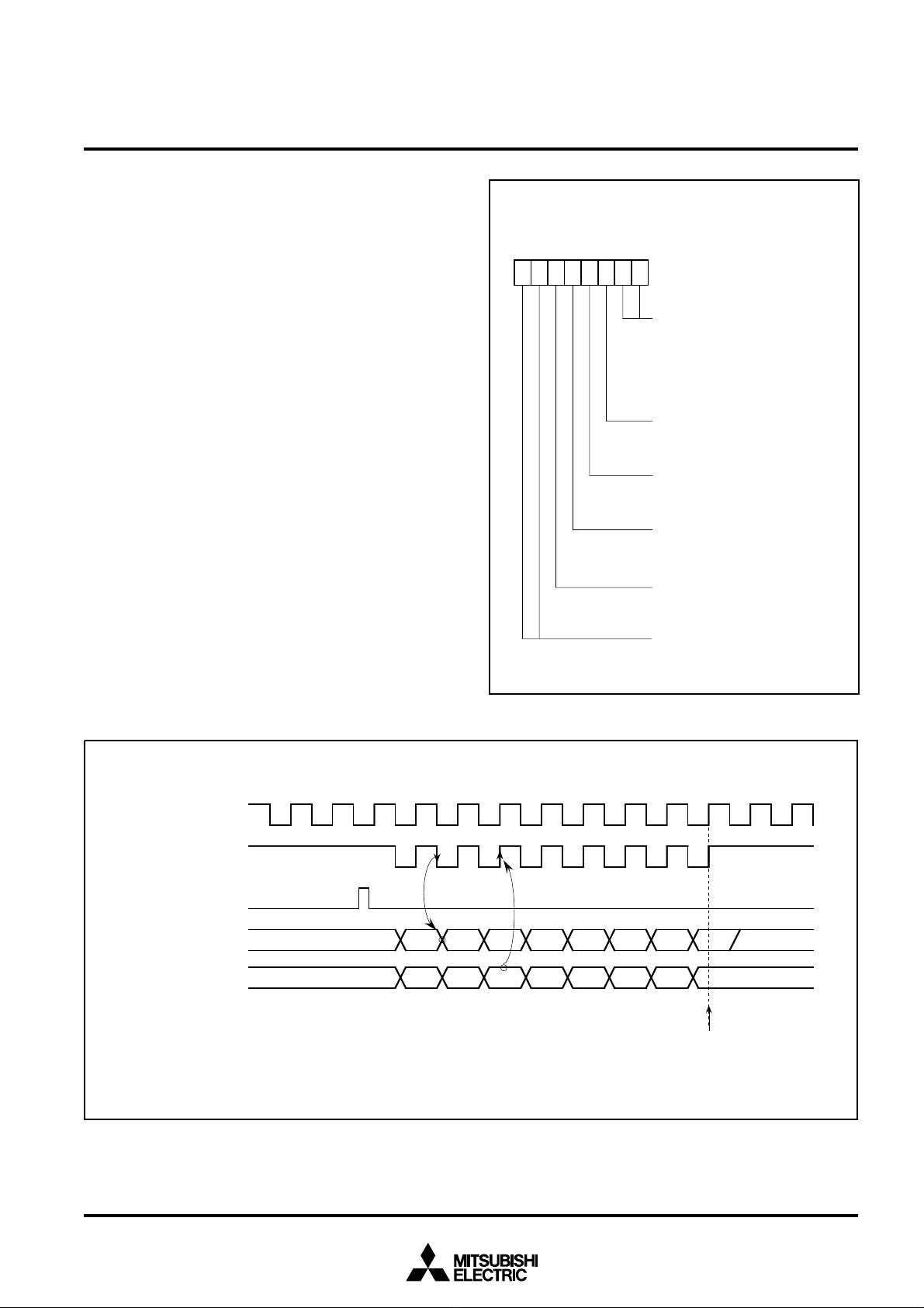
The serial I/O timing is shown in Figure 13. When using an external
clock for transfer, the external clock must be held at “H” for initializing
the serial I/O counter. When switching between an internal clock and
an external clock, do not switch during transfer. Also, be sure to initialize the serial I/O counter after switching.
Notes 1: On programming, note that the serial I/O counter is set by
writing to the serial I/O register with the bit managing instructions as SEB and CLB instructions.
2: When an external clock is used as the synchronizing clock,
write transmit data to the serial I/O register at “H” of the
transfer clock input level.
7
0
and ON-SCREEN DISPLAY CONTROLLER
0
0
Serial I/O mode register
(SM : address 0213
Internal synchronizing clock
selection bits
b1 b0
0 0 : f(X
IN)/8 or f(XCIN)/8
0 1 : f(XIN)/16 or f(XCIN)/16
1 0 : f(X
IN)/32 or f(XCIN)/32
1 1 : f(XIN)/64 or f(XCIN)/64
Synchronizing clock selection bit
0 : External clock
1 : Internal clock
Port function selection bit
1, P13 functions as port
0 : P1
1 : SCL1, SDA1
Port function selection bit
0 : P12, P14 functions as port
1 : SCL2, SDA2
Transfer direction selection bit
0 : LSB first
1 : MSB first
Fix these bits to “0”
16)
Synchroninzing clock
Transfer clock
Serial I/O register
write signal
Serial I/O output
S
Serial I/O input
Note : When an internal clock is selected, the S
S
OUT
IN
Fig. 13. Serial I/O timing (for LSB first)
Fig. 14. Structure of serial I/O mode register
D
0
D
1
D
2
D
3
D
4
D
OUT
pin is at high-impedance after transfer is completed.
(Note)
5
D
6
D
7
Interrupt request bit is set to “1”
21

MITSUBISHI MICROCOMPUTERS
M37271MF-XXXSP
M37271EF-XXXSP, M37271EFSP
SINGLE-CHIP 8-BIT CMOS MICROCOMPUTER with CLOSED CAPTION DECODER
and ON-SCREEN DISPLAY CONTROLLER
PWM OUTPUT FUNCTION
The M37271MF-XXXSP is equipped with seven 8-bit PWMs (PWM0–
PWM6). PWM0–PWM6 have the same circuit structure and an 8-bit
resolution with minimum resolution bit width of 4 µs (for f(XIN) = 8
MHz) and repeat period of 1024 µs.
Figure 15 shows the PWM block diagram. The PWM timing generating circuit applies individual control signals to PWM0–PWM6 using
f(XIN) divided by 2 as a reference signal.
(1) Data Setting
When outputting PWM0–PWM6, set 8-bit output data in the PWMi
register (i means 0 to 6; addresses 020016 to 020616).
(2) Transmitting Data from Register to PWM circuit
Data transfer from the 8-bit PWM register to 8-bit PWM circuit is
executed at writing data to the register.
The signal output from the 8-bit PWM output pin corresponds to the
contents of this register.
(3) Operating of 8-bit PWM
The following is the explanation about PWM operation.
At first, set the bit 0 of PWM mode register 1 (address 020A16) to “0”
(at reset, bit 0 is already set to “0” automatically), so that the PWM
count source is supplied.
PWM0–PWM3 are also used as pins P04–P07, PWM4–PWM6 are
also used as pins P00–P02, respectively. Set the corresponding bits
of the port P0 direction register to “1” (output mode). And select each
output polarity by bit 3 of the PWM mode register 1 (address 020A16).
Then, set bits 7 to 0 of the PWM output control register 2 to “1”
(PWM output).
The PWM waveform is output from the PWM output pins by setting
these registers.
Figure 16 shows the 8-bit PWM timing. One cycle (T) is composed
of 256 (28) segments. The 8 kinds of pulses relative to the weight of
each bit (bits 0 to 7) are output inside the circuit during 1 cycle. Refer
to Figure 16 (a). The 8-bit PWM outputs waveform which is the logical sum (OR) of pulses corresponding to the contents of bits 0 to 7 of
the 8-bit PWM register. Several examples are shown in Figure 16
(b). 256 kinds of output (“H” level area: 0/256 to 255/256) are selected by changing the contents of the PWM register. A length of
entirely “H” output cannot be output, i.e. 256/256.
(4) Output after Reset
At reset, the output of ports P00–P02 and P04–P07 is in the highimpedance state, port P50 outputs “L,” and the contents of the PWM
register and the PWM circuit are undefined. Note that after reset, the
PWM output is undefined until setting the PWM register.
22
MITSUBISHI MICROCOMPUTERS
M37271MF-XXXSP
M37271EF-XXXSP, M37271EFSP
Data bus
X
PWM0 register
(Address 0200
SINGLE-CHIP 8-BIT CMOS MICROCOMPUTER with CLOSED CAPTION DECODER
16
PWM timing
generating
circuit
)
IN
1/2
ENABLE
b7 b0
and ON-SCREEN DISPLAY CONTROLLER
Selection gate :
Connected to
black colored
side at reset.
Inside of
8
8-bit PWM circuit
PWM1 register (Address 020116)
PWM2 register (Address 020216)
PWM3 register (Address 020316)
PWM4 register (Address 020416)
PWM5 register (Address 020516)
PWM6 register (Address 020616)
is as same contents with the others.
POL
P0
D0
4
4
PW0
D0
P0
5
5
PW1
D0
P0
6
6
PW2
D0
P0
7
7
PW3
D0
P0
0
0
PW4
D0
P0
1
1
PW5
D0
P0
2
2
PW6
: PWM mode register 1 (address 020A
PN
: PWM mode register 2 (address 020B
PW
: Port P0 register (address 00C0
P0
: Port P0 direction register (address 00C1
D0
16
)
PWM0
PWM1
PWM2
PWM3
PWM4
PWM5
PWM6
16
16
)
)
16
)
Fig. 15. PWM block diagram
23
(a) Pulses showing the weight of each bit
1 3 5 7 9 20 30 40 50 60 70 80 90 100 110 120 130 140 150 160 170 180 190 200 210 220 230 240 250 255
4 12 20 28 36 44 52 60 68 76 84 92 100 108 116 124 132 140 148 156 164 172 180 188 196 204 212 220 228 236 244 252
8
16 48 80 112 144 176 208 240
24
40 56
72 88
104 120
136 152
168 184
200 216
232 248
32
96
160
224
64
192
Bit 7
2 6 10 14 18 22 26 30 34 38 42 46 50 54 58 62 66 70 74 78 82 86 90 94 98 102 106 110 114 118 122 126 130 134 138 142 146 150 154 158 162 166 170 174 178 182 186 190 194 198 202 206 210 214 218 222 226 230 234 238 242 246 250 254
Bit 6
Bit 5
Bit 4
Bit 3
Bit 2
Bit 1
128
Bit 0
PWM output t = 4
µ
s T = 1024
µ
s
f(X
IN
) = 8 MHz
(b) Example of 8-bit PWM
t
00
16
(0)
01
16
(1)
18
16
(24)
FF
16
(255)
T = 256 t
MITSUBISHI MICROCOMPUTERS
M37271MF-XXXSP
M37271EF-XXXSP, M37271EFSP
SINGLE-CHIP 8-BIT CMOS MICROCOMPUTER with CLOSED CAPTION DECODER
and ON-SCREEN DISPLAY CONTROLLER
Fig. 16. 8-bit PWM timing
24
MITSUBISHI MICROCOMPUTERS
M37271MF-XXXSP
M37271EF-XXXSP, M37271EFSP
SINGLE-CHIP 8-BIT CMOS MICROCOMPUTER with CLOSED CAPTION DECODER
PWM mode register 1
(PN: address 020A
16
)
0
and ON-SCREEN DISPLAY CONTROLLER
07
PWM mode register 2
(PW: address 020B
16
)
PWM count source selection bit
0 : Count source supply
1 : Count source stop
PWM output polarity selection bit
0 : Positive polarity
1 : Negative polarity
P04/PWM0 output selection bit
0 : P0
4
output
1 : PWM0 output
5
/PWM1 output selection bit
P0
5
0 : P0
output
1 : PWM1 output
P0
6
/PWM2 output selection bit
6
0 : P0
output
1 : PWM2 output
P0
7
/PWM3 output selection bit
7
0 : P0
output
1 : PWM3 output
P0
0
/PWM4 output selection bit
0
0 : P0
output
1 : PWM4 output
1
/PWM5 output selection bit
P0
1
0 : P0
output
1 : PWM5 output
P0
2
/PWM6 output selection bit
2
0 : P0
output
1 : PWM6 output
Fig. 17. Structure of PWM-related registers
Fix this bit to “0.”
25
MITSUBISHI MICROCOMPUTERS
M37271MF-XXXSP
M37271EF-XXXSP, M37271EFSP
SINGLE-CHIP 8-BIT CMOS MICROCOMPUTER with CLOSED CAPTION DECODER
and ON-SCREEN DISPLAY CONTROLLER
A-D CONVERTER
(1)A-D Conversion Register (AD)
A-D conversion reigister is a read-only register that stores the result
of an A-D conversion. This register should not be read during A-D
conversion.
(2)A-D Control Register (ADCON)
The A-D control register controls A-D conversion. Bits 1 and 0 of this
register select analog input pins. When these pins are not used as
anlog input pins, they are used as ordinary I/O pins. Bit 3 is the A-D
conversion completion bit, A-D conversion is started by writing “0” to
this bit. The value of this bit remains at “0” during an A-D conversion,
then changes to “1” when the A-D conversion is completed.
Bit 4 controls connection between the resistor ladder and VCC. When
not using the A-D converter, the resistor ladder can be cut off from
the internal VCC by setting this bit to “0.” This can realize the lowpower dissipation.
(3)Comparison Voltage Generator (Resistor
Ladder)
The voltage generator divides the voltage between VSS and VCC by
256, and outputs the divided voltages to the comparator as the reference voltage Vref.
(4)Channel Selector
The channel selector connects an analog input pin selected by bits 1
and 0 of the A-D control register to the comparator.
(5)Comparator and Control Circuit
The conversion result of the analog input voltage and the reference
voltage “Vref” is stored in the A-D conversion register. The A-D conversion completion bit and A-D conversion interrupt request bit are
set to “1” at the completion of A-D conversion.
70
0
Fig. 18. Structure of A-D control register
A-D control register
(ADCON: address 00EF16)
Analog input pin selection bits
b1 b0
0 0 : P26/AD1
0 1 : P25/AD2
1 0 : P24/AD3
1 1 : P40/AD4
A-D conversion completion bit
0 : Conversion in purogress
1 : Conversion completed
VCC connection selection bit
0 : OFF
1 : ON
Fix this bit to “0.”
A-D control register
(address 00EF
P26/AD1
5
/AD2
P2
4
/AD3
P2
P4
0
/AD4
Fig. 19. A-D comparator block diagram
16
)
Comparator
Channel selector
Data bus
b7 b0
2
A-D control circuit
A-D conversion register
Switch tree
Resistor ladder
VSSV
8
(address 00EE16)
CC
A-D conversion
interrupt request
26
MITSUBISHI MICROCOMPUTERS
M37271MF-XXXSP
M37271EF-XXXSP, M37271EFSP
SINGLE-CHIP 8-BIT CMOS MICROCOMPUTER with CLOSED CAPTION DECODER
and ON-SCREEN DISPLAY CONTROLLER
(6) Conversion Method
1Set bit 7 of the interrupt interval determination control register (ad-
dress 021216) to “1” to generate an interrupt request at completion of A-D conversion.
2Set the A-D conversion · INT3 interrupt request bit to “0” (even
when A-D conversion is started, the A-D conversion · INT3 interrupt bit is not set to “0” automatically).
3When using A-D conversion interrupt, enable interrupts by setting
A-D conversion · INT3 interrupt request bit to “1” and setting the
interrupt disable flag to “0.”
4Set the VCC connection selection bit to “1” to connect VCC to the
resistor ladder.
5Select analog input pins by setting the analog input selection bit of
the A-D control register.
6Set the A-D conversion completion bit to “0.” This write operation
starts the A-D conversion. Do not read the A-D conversion register during the A-D conversion.
7Verify the completion of the conversion by the state (“1”) of the
A-D conversion completion bit, that (“1”) of A-D conversion · INT3
interrupt bit, or the occurrence of an A-D conversion interrupt.
8Read the A-D conversion register to obtain the conversion results.
Note : When the ladder resistor is disconnect from VCC, set the VCC
connection selection bit to “0” between steps 7and 8.
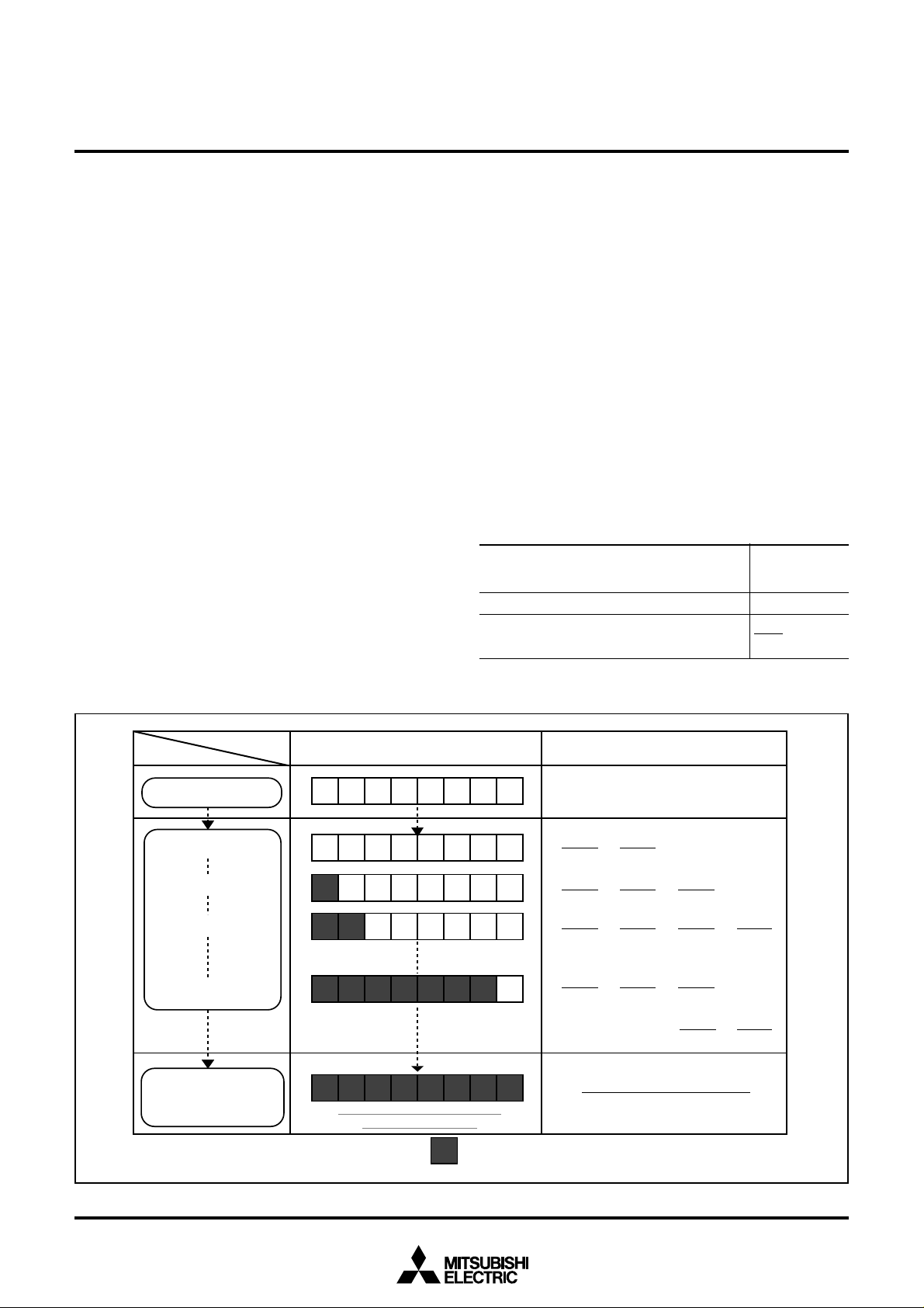
(7) Internal Operation
At the time when the A-D conversion starts, the following operations
are automatically performed.
1The A-D conversion register is set to “0016.”
2The most significant bit of the A-D conversion register becomes
“1, ” and the comparison voltage “Vref” is input to the comparator.
At this point, Vref is compared with the analog input voltage “VIN .”
3Bit 7 is determined by the comparison result as follows.
When Vref < VIN : bit 7 holds “1”
When Vref > VIN : bit 7 becomes “0”
With the above operations, the analog value is converted into a digital value. The A-D conversion terminates in a maximum 50 machine
cycles (12.5 µs at f(XIN) = 8 MHz) after it starts, and the conversion
result is stored in the A-D conversion register.
An A-D conversion interrupt request occurs at the same time of A-D
conversion completion, the A-D conversion · INT3 interrupt request
bit becomes “1.” The A-D conversion completion bit also becomes
“1.”
Table 2. Expression for Vref and VREF
A-D conversion register contents “n”
(decimal notation)
00
Note: VREF indicates the voltage of internal VCC.
VREF
256
Vref (V)
✕ (n – 0.5)1 to 255
A-D conversion start
1st comparison start
2nd comparison start
3rd comparison start
Contents of A-D conversion register
00000000
1
0000000
1000000
1
12
100000
Reference voltage (V
V
REF
–
2
V
REF
±
2
V
REF
±
2
V
REF
8th comparison start
A-D conversion completion
(8th comparison completion)
Fig. 20. Changes in A-D conversion register and comparison voltage during A-D conversion
1234567
1
12345678
Digital value corresponding to
analog input voltage.
m
: Value determined by mth (m = 1 to 8) result
±±±
2
V
REF
512
V
REF
4
V
REF
4
V
REF
4
.......
ref
)
[V]
0
V
REF
–
512
V
REF
±
8
V
REF
8
REF
V
±
256
V
REF
–
512
.....
REF
V
–
512
27
MITSUBISHI MICROCOMPUTERS
M37271MF-XXXSP
M37271EF-XXXSP, M37271EFSP
SINGLE-CHIP 8-BIT CMOS MICROCOMPUTER with CLOSED CAPTION DECODER
and ON-SCREEN DISPLAY CONTROLLER
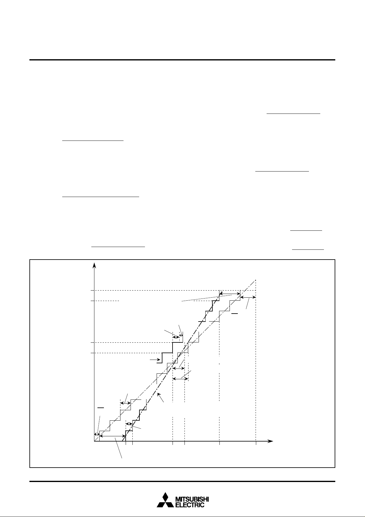
(8) Definition of A-D Conversion Accuracy
The definition of A-D conversion accuracy is described below.
1Relative accuracy
· Zero transition error (V0T)
The deviation of the input voltage at which A-D conversion output
data changes from “0” to “1,” from the corresponding ideal A-D
conversion characteristics between 0 and VREF.
V0T =
· Full-scale transition error (VFST)
The deviation of the input voltage at which A-D conversion output
data changes from “255” to “254,” from the corresponding ideal AD conversion characteristics between 0 and VREF.
VFST =
· Non-linearity error
The deviation of the actual A-D conversion characteristics, from the
ideal A-D conversion characteristics between V0 and V254.
Non-linearity error =
(V0 –1/2 ✕ VREF/256)
1LSB
(VREF – 3/2 ✕ VREF/256) – V254
1LSB
Vn – (1LSB ✕ n + V0)
1LSB
[LSB]
[LSB]
[LSB]
· Differential non-linearity error
The deviation of the input voltage required to change output data
by “1,” from the corresponding ideal A-D conversion characteristics between 0 and VREF.
(Vn+1 – Vn) – 1LSB
1LSB
2Absolute accuracy
· Absolute accuracy error
The deviation of the actual A-D conversion characteristics, from the
ideal A-D conversion characteristics between 0 and VREF.
Absolute accuracy error =
Note: The analog input voltage “Vn” at which A-D conversion output
data changes from “n” to “n + 1” (n ; 0 to 254) is as follows
(refer to Figure 18).
1LSB with respect to relative accuracy =
1LSBA with respect to absolute accuracy =
Vn – 1LSBA ✕ (n+1/2)
1LSBA
V254 – V0
254
VREF
256
[LSB]Differential non-linearity error =
[LSB]
[V]
[V]
Output
data
255
254
n+1
n
Actual A-D
conversion
characteristics
1
2
0
Full-scale transition error
(V
FST
)
Differential nonlinearity error
A
1LSB
A
LSB
1LSB
V
0
V
1
Zero transition error (V0T)
1LSB
Non-linearity error
Absolute accuracy
Ideal A-D conversion characteristics
between V
VnV
0
and V
n+1
254
V
254
3
LSB
A
2
Analog input
V
REF
voltage (V)
Fig. 21. Definition of A-D conversion precision
28
MITSUBISHI MICROCOMPUTERS
M37271MF-XXXSP
M37271EF-XXXSP, M37271EFSP
SINGLE-CHIP 8-BIT CMOS MICROCOMPUTER with CLOSED CAPTION DECODER
and ON-SCREEN DISPLAY CONTROLLER
DATA SLICER
The M37271MF-XXXSP includes the data slicer function for the
closed caption decoder (referred to as the CCD). This function takes
out the caption data superimposed in the vertical blanking interval of
a composite video signal. A composite video signal which makes
the sync chip’s polarity negative is input to the CVIN pin.
Composite
video
signal
Hundred of kiloohms
to 1 MΩ
V
HOLD
1000 pF
External circuit
Note: Make the length of wiring which is
connected to V
and CV
so that a leakage current may
not be generated when mounting
a resistor or a capacitor on each
pin.
HOLD, HLF, RVCO
IN pin as short as possible
Sync slice
(address
0.1µF
Low-pass
filter
Reference
voltage
generating
circuit
register 3
00E316)
0000101
470Ω
IN
CV
Clamping
circuit
Sync slice
circuit
+
–
Comparator
Data slicer control
register 3
(address 0210
Clock run-in detect
register 3
(address 0208
Clock run-in
register 3
(address 0209
Data register 2
(address 00E5
16)
16)
16)
16)
560 pF
Data register 4
(address 00ED
1µF
H
When the data slicer function is not used, the data slicer circuit can
be cut off by setting bit 0 of the data slicer control register 1 (address
00EA16) to “0.” Also, the timing signal generating circuit can be cut
off by setting bit 0 of data slicer control register 2 (address 00EB16)
to “0.” These settings can realize the low-power dissipation.
1 kΩ
200 pF
SYNC
Synchronizing
signal counter
Synchronizing
separation
circuit
Timing signal
generating
circuit
Clock run-in
determination
circuit
Data slice line
specification
circuit
Start bit detecting
circuit
Data clock
generating circuit
16-bit shift register
high-order low-order
Data register 1
(address 00E4
16)
15 kΩ
HLF RVCO
16)
Interrupt request
generating circuit
Data register 3
(address 00EC
Sync pulse counter
register
16
(address 020F
)
Clock run-in register 2
16
(address 00E7
)
01 0111
Data slicer control register 2
16
(address 00EB
00
)
0
Data slicer control register 1
16
(address 00EA
)
000
Data slicer ON/OFF
Window register
(address 00E2
16
)
00
0101
Clock run-in register 1
(address 00E6
16
)
100
Caption position register
(address 00E0
16
)
Start bit position register
16
(address 00E1
)
Clock run-in detect register 1
(address 00E8
16
)
Clock run-in detect register 2
(address 00E9
16
)
Data slicer
interrupt
request
16)
Data bus
Fig. 22. Data slicer block diagram
29
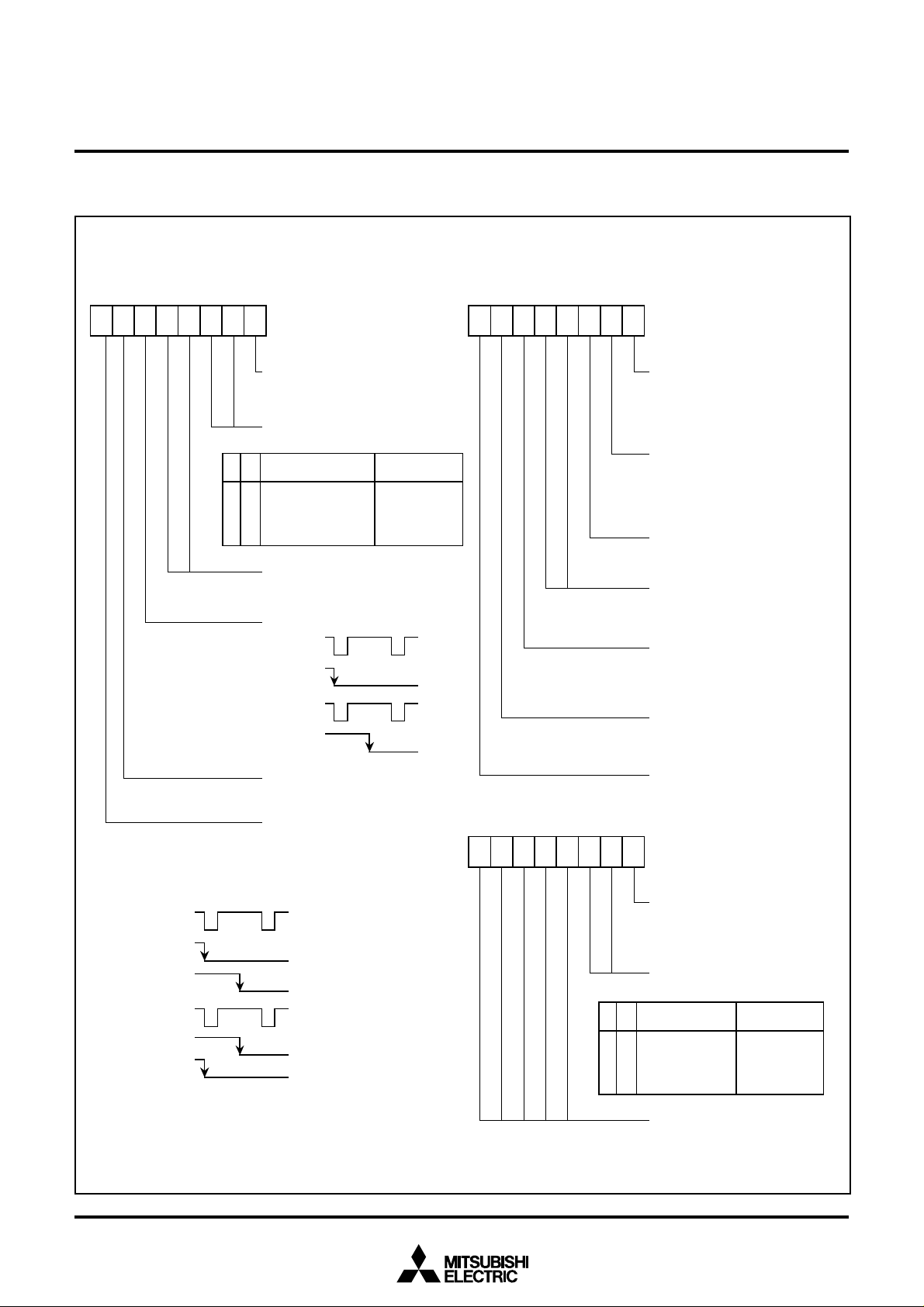
MITSUBISHI MICROCOMPUTERS
M37271MF-XXXSP
M37271EF-XXXSP, M37271EFSP
SINGLE-CHIP 8-BIT CMOS MICROCOMPUTER with CLOSED CAPTION DECODER
and ON-SCREEN DISPLAY CONTROLLER
Figure 23 shows the structure of the data slicer control registers.
000
b2 b1
0 0 F2
0 1 F1
1 0 F1 and F2
1 1 F1 and F2
07
Data slicer control register 1
16
(DSC1: address 00EA
)
Data slicer control bit
0: Data slicer stopped
1: Data slicer operating
Field to be sliced data selection bit
Field of main data
slice line
Field for setting
reference voltage
F2
F1
F2
F1
Fix these bits to “0.”
Field determination flag
sep
0 :
H
sep
V
sep
H
1 :
sep
V
000
07
Data slicer control register 2
(DSC2: address 00EB
16
)
Timing signal generating circuit
control bit
0: Stopped
1: Operating
Reference clock source selection
bit
0: Video signal
SYNC
1: H
signal
Test bit: read-only
Fix these bits to “0.”
V-pulse shape determination flag
0: Match
1: Mismatch
Fix this bit to “0.”
Fix this bit to “0.”
Data latch completion flag for caption
data in main data slice line
0: Data is not yet latched
1: Data is latched
Definition of fields 1 (F1) and 2 (F2)
sep
H
F1 :
SYNC
V
sep
V
sep
H
F2 :
SYNC
V
sep
V
Fig. 23. Structure of data slicer control registers
Test bit: read-only
07
Data slicer control register 3
(DSC3: address 0210
Line selection bit for slice voltage
0: Main data slice line
1: Sub-data slice line
Field to be sliced data selection bit
Field of sub-data
b2 b1
slice line
0 0 F2
0 1 F1
1 0 F1 and F2
1 1 F1 and F2
Setting bit of sub-data slice line
16
)
Field for setting
reference voltage
F2
F1
F2
F1
30

MITSUBISHI MICROCOMPUTERS
M37271MF-XXXSP
M37271EF-XXXSP, M37271EFSP
SINGLE-CHIP 8-BIT CMOS MICROCOMPUTER with CLOSED CAPTION DECODER
(1) Clamping Circuit and Low-pass Filter
This filter attenuates the noise of the composite video signal input
from the CVIN pin. The CVIN pin to which composite video signal is
input requires a capacitor (0.1 µF) coupling outside. Pull down the
CVIN pin with a resistor of hundreds of kiloohms to 1 M . In addition,
we recommend to install externally a simple low-pass filter using a
resistor and a capacitor at the CVIN pin (refer to Figure 22).
000
and ON-SCREEN DISPLAY CONTROLLER
07
0011
Sync slice register
(SSL : address 00E3
Fix these bits to “0000101
16
)
2
”
(2) Sync Slice Circuit
This circuit takes out a composite sync signal from the output signal
of the low-pass filter. Figure 24 shows the structure of the sync slice
register.
(3) Synchronizing Signal Separation Circuit
This circuit separates a horizontal synchronizing signal and a vertical
synchronizing signal from the composite sync signal taken out in the
sync slice circuit.
1Horizontal synchronizing signal (Hsep)
A one-shot horizontal synchronizing signal Hsep is generated at
the falling edge of the composite sync signal.
2 Vertical synchronizing signal (Vsep)
As a Vsep signal generating method, it is possible to select one of
the following 2 methods by using bit 7 of the sync slice register
(address 00E316).
•Method 1 The “L” level width of the composite sync signal is
measured. If this width exceeds a certain time, a Vsep
signal is generated in synchronization with the rising
of the timing signal immediately after this “L” level.
•Method 2 The “L” level width of the composite sync signal is
measured. If this width exceeds a certain time, it is
detected whether a falling of the composite sync
signal exits or not in the “L” level period of the timing
signal immediately after this “L” level. If a falling exists,
a Vsep signal is generated in synchronization with
the rising of the timing signal (refer to Figure 25).
Figure 25 shows a Vsep generating timing. The timing signal shown
in the figure is generated from the reference clock which the timing
generating circuit outputs.
Reading bit 5 of data slicer control register 2 permits determinating
the shape of the V-pulse portion of the composite sync signal. As
shown in Figure 26, when the A level matches the B level, this bit is
“0.” In the case of a mismatch, the bit is “1.”
For the pins RVCO and the HLF, connect a resistor and a capacitor
as shown in Figure 22. Make the length of wiring which is connected
to these pins as short as possible so that a leakage current may not
be generated.
Vertical synchronizing
signal (V
method selection bit
0 : Method 1
1 : Method 2
Fig. 24. Structure of sync slice register
Composite
sync signal
Measure “L” period
Timing
signal
V
sep
signal
sep
signal is generated at a rising of the timing signal
A V
immediately after the “L” level width of the composite
sync signal exceeds a certain time.
Fig. 25. Vsep generating timing (method 2)
sep
) generating
Note: It takes a few tens of milliseconds until the reference clock
becomes stable after the data slicer and the timing signal
generating circuit are started. In this period, various timing
signals, Hsep signals and Vsep signals become unstable. For
this reason, take stabilization time into consideration when
programming.
31

MITSUBISHI MICROCOMPUTERS
M37271MF-XXXSP
M37271EF-XXXSP, M37271EFSP
SINGLE-CHIP 8-BIT CMOS MICROCOMPUTER with CLOSED CAPTION DECODER
and ON-SCREEN DISPLAY CONTROLLER
(4) Timing Signal Generating Circuit
This circuit generates a reference clock which is 832 times as large
as the horizontal synchronizing signal frequency. It also generates
various timing signals on the basis of the reference clock, horizontal
synchronizing signal and vertical synchronizing signal. The circuit
operates by setting bit 0 of data slicer control register 2 (address
00EB16) to “1.”
The reference clock can be used as a display clock for OSD function
in addition to the data slicer. The HSYNC signal can be used as a
count source instead of the composite sync signal. However, when
the HSYNC signal is selected, the data slicer cannot be used. A count
source of the reference clock can be selected by bit 1 of data slicer
control register 2 (address 00EB16).
Composite
sync signal
V-pulse
(“L” pulse width is long,
“H” pulse width is short)
AB
Bit 5 of
DSC2
0
1
1
Fig. 26. Determination of V-pulse waveform
32

MITSUBISHI MICROCOMPUTERS
M37271MF-XXXSP
M37271EF-XXXSP, M37271EFSP
SINGLE-CHIP 8-BIT CMOS MICROCOMPUTER with CLOSED CAPTION DECODER
and ON-SCREEN DISPLAY CONTROLLER
(5) Data Slice Line Specification Circuit
1 Specification of data slice line
M37271MF-XXXSP has 2 data slice line specification circuits for
slicing arbitrary 2 Hsep in 1 field. The following 2 data slice lines
are specified .
<Main data slice line>
This line is specified by the caption position register (address
00E016).
<Sub-data slice line>
This line is specified by the data slicer control register 3 (address
00EB16).
The counter is reset at the falling edge of Vsep and is incremented
by 1 every Hsep pulse. When the counter value matched the value
specified by bits 4 to 0 of the caption position register (in case of
the sub-data slice line, by bits 3 to 7 of the data slicer control register
3), this Hsep is sliced.
The values of “0016” to “1F16” can be set in the caption position
register. Bit 7 to bit 5 are used for testing. Set “1002.” Figure 27
shows the signals in the vertical blanking interval. Figure 28 shows
the structure of the caption position register.
Table 3. Specifying of field whose sets reference voltage
Bit 0 of DSC3
0
1
DSC1 : Data slice control register 1
DSC3 : Data slice control register 3
CP : Caption position register
Field specified by bit 1 of DSC1 0: F2 1: F1
Field specified by bit 1 of DSC3 0: F2 1: F1
Field
2 Selection of field to be sliced data
In the case of the main data slice line, the field to be sliced data is
selected by bits 2 and 1 of the data slicer control register 1 (address
00EA16). In the case of the sub-data slice line, the field is selected
by bits 2 and 1 of the data slicer control register 3. When bit 2 of
the data slicer control register 1 is set to “1,” it is possible to slice
data of both fields (refer to Figure 23).
3 Specification of line to set slice voltage
The reference voltage for slicing (slice voltage) is generated by
integrating the amplitude of the clock run-in pulse in the particular
line (refer to Table 3).
4 Field determination
The field determination flag can be read out by bit 5 of the data
slicer control register 1. This flag charge at the falling edge of
Vsep.
Line
Line specified by bits 4 to 0 of CP
(Main data slice line)
Line specified by bits 7 to 3 of DSC3
(Sub-data slice line)
Video signal
Composite
video signal
V
H
sep
sep
H
sep
Composite video
signal
Vertical blanking interval
Count value to be set in the caption position register (“11
Clock run-in Start bit + 16-bit data
Start bit
max.
min.
Time to be set in the
start bit position register
16
” in this case)
Line 21
Magnified
drawing
Fig. 27. Signals in vertical blanking interval
33

MITSUBISHI MICROCOMPUTERS
M37271MF-XXXSP
M37271EF-XXXSP, M37271EFSP
SINGLE-CHIP 8-BIT CMOS MICROCOMPUTER with CLOSED CAPTION DECODER
and ON-SCREEN DISPLAY CONTROLLER
(6) Reference Voltage Generating Circuit and
Comparator
The composite video signal clamped by the clamping circuit is input
to the reference voltage generating circuit and the comparator.
1Reference voltage generating circuit
This circuit generates a reference voltage (slice voltage) by using
the amplitude of the clock run-in pulse in line specified by the data
slice line specification circuit. Connect a capacitor between the
VHOLD pin and the VSS pin, and make the length of wiring as short
as possible so that a leakage current may not be generated.
2Comparator
The comparator compares the voltage of the composite video signal
with the voltage (reference voltage) generated in the reference
voltage generating circuit, and converts the composite video signal
into a digital value.
70
100
Fig. 28. Structure of caption position register
Caption position register
(CP : address 00E0
Specification main data slice line
Fix these bits to “1002”
16)
(7) Start Bit Detecting Circuit
This circuit detects a start bit at line decided in the data slice line
specification circuit. For start bit detection, it is possible to select one
of the following two types by using bit 1 of the clock run-in register 2
(address 00E716).
1After the lapse of the time corresponding to the set value of the
start bit position register (address 00E116), the first rising of the
composite video signal is detected as a start bit.
The time is set in bits 0 to 6 of the start bit position register (address
00E116) (refer to Figure 26). Set a value fit for the following
conditions.
Figure 29 shows the structure of the start bit position register.
Time from the falling of the horizontal
synchronizing signal to the last rising
of the clock run-in
4 ✕ set value of the start bit position
register ✕ reference clock period
<<
70
Fig. 29. Structure of start bit position register
Start bit position register
(SP : address 00E1
Start bit generating time
Time from a falling of the
horizontal synchronizing signal
to occurrence of a start bit = 4
✕ set value (“00
reference clock period
DSC1 bit 7 control bit
0 : Generation of 16 pulses
1 : Generation of 16 pulses and
detection of clock run-in
Time from the falling of the horizontal
synchronizing signal to occurrence of
the start bit
16
)
16”
to “7F16”) ✕
34

MITSUBISHI MICROCOMPUTERS
M37271MF-XXXSP
M37271EF-XXXSP, M37271EFSP
SINGLE-CHIP 8-BIT CMOS MICROCOMPUTER with CLOSED CAPTION DECODER
2After a falling of the clock run-in pulse set in bits 2 to 0 of clock run-
in detect register 2 (address 00E916) is detected, a start bit is
detected by sampling a comparator output. A sampling clock for
sampling is obtained by dividing the reference clock generated in
the timing signal generating circuit by 13.
Figure 31 shows the structure of clock run-in detect register 2.
The contents of bits 2 to 0 of clock run-in detect register 2 and bit
1 of clock run-in register 2 are written at a falling of the horizontal
synchronizing signal. For this reason, even if an instruction for
setting is executed, the contents of the register cannot be rewritten
until a falling of the horizontal synchronizing signal.
and ON-SCREEN DISPLAY CONTROLLER
70
1
00111 1
Fig. 30. Structure of clock run-in register 2
Clock run-in register 2
(CR2 : address 00E7
Fix this bit to “1”
Start bit detecting method
selection bit
0 : Method 1
1 : Method 2
Fix these bits to “100111
70
16
)
2
”
Fig. 31. Structure of clock run-in detect register 2
Clock run-in detect register 2
(CRD2 : address 00E9
Clock run-in pulses for sampling
b2 b1 b0
0 0 0 : Not available
0 0 1 : 1st pulse
0 1 0 : 2nd pulse
0 1 1 : 3rd pulse
1 0 0 : 4th pulse
1 0 1 : 5th pulse
1 1 0 : 6th pulse
1 1 1 : 7th pulse
Data clock generating time
Time from detection of a start bit
to occurrence of a data clock
= (13 + set value) ✕ reference
clock period
16
)
(8) Clock run-in determination circuit
This circuit sets a window in the clock run-in portion in the composite
video signal, and then determinates clock run-in by counting the
number of pulses in this window. Set the time from a falling of the
horizontal synchronizing signal to a start of the window by bits 0 to 5
of the window register (address 00E216; refer to Figure 32). The
window ends according to the contents of the setting of the start bit
position register (refer to Figure 29).
70
00
Fig. 32. Structure of window register
Window register
(WN : address 00E2
Window start time
Time from a falling of the
horizontal synchronizing signal
to a start of the window = 4 ✕ set
value (“00
clock period
Fix these bits to “0”
16
)
16
” to “3F16”) ✕ reference
35

70
Number of reference clocks to
be counted in one clock run-in
pulse period
Clock run-in detect registers 1, 3
( CRD1 : address 00E8
16
)
( CRD3 : address 0208
16
)
Test bits : read-only
MITSUBISHI MICROCOMPUTERS
M37271MF-XXXSP
M37271EF-XXXSP, M37271EFSP
SINGLE-CHIP 8-BIT CMOS MICROCOMPUTER with CLOSED CAPTION DECODER
and ON-SCREEN DISPLAY CONTROLLER
For the main data slice line, the count value of pulses in the window
is stored in clock run-in register 1 (address 00E616; refer to Figure
33). For the sub-data slice line, the count value of pulses in the window
is stored in clock run-in register 3 (address 020916; refer to Figure
34). When this count value is 4 to 6, it is determined as a clock run-in.
Accordingly, set the count value so that the window may start after
the first pulse of the clock run-in (refer to Figure 35).
The contents to be set in the window register are written at a falling
of the horizontal synchronizing signal. For this reason, even if an
instruction for setting is executed, the contents of the register cannot
be rewritten until a falling of the horizontal synchronizing signal.
For the main data slice line, reference clock is counted in the period
from a falling of the clock pulse set in bits 0 to 2 of the clock run-in
detect register 2 (address 00E916) to the next falling. The count value
is stored in bits 3 to 7 of the clock run-in detect register 1 (address
00E816) (When the count value exceeds “1F16,” “1F16” is held). For
the sub-data slice line, the count value is stored in bits 3 to 7 of the
clock run-in detect register 3 (address 020816). Read out these bits
after the occurence of a data slicer interrupt (refer to (11) Interrupt
Request Generating Circuit).
Figure 36 shows the structure of clock run-in detect registers 1 and
3.
70
0101
Clock run-in register 1
(CR1 : address 00E6
Clock run-in count value of
main-data slice line
Fix these bits to “0101
Fig. 33. Structure of clock run-in register 1
70
Clock run-in register 3
(CR3 : address 0209
Clock run-in count value of sub-data
slice line
Data latch completion flag for caption data in
sub-data slice line
0: Data is not latched yet
1: Data is latched
Data slice line selection bit for interrupt
request
0: Main data slice line
1: Sub-data slice line
Interrupt mode selection bit
0: Interrupt occurs at end of data slice line
1: Interrupt occurs at completion of caption
data latch
16
)
2
”
16
)
Fig. 34. Structure of clock run-in register 3
Horizontal
synchronizing
signal
Clock run-in
Start bit data +
16-bit data
Composite
video signal
Window
Time to be set in the
window register
Time to be set in
✽When the count value
in the window is 4 to 6,
this is determined as a
clock run-in.
the start bit position
register
Fig. 35. Window setting
Fig. 36. Structure of clock run-in detect registers 1and 3
36

MITSUBISHI MICROCOMPUTERS
M37271MF-XXXSP
M37271EF-XXXSP, M37271EFSP
SINGLE-CHIP 8-BIT CMOS MICROCOMPUTER with CLOSED CAPTION DECODER
and ON-SCREEN DISPLAY CONTROLLER
(9) Data clock generating circuit
This circuit generates a data clock phase-synchronized with the start
bit detected in the start bit detecting circuit.
Set the time from detection of the start bit to occurrence of the data
clock in bits 3 to 7 of the clock run-in detect register 2 (address
00E916). The time to be set is represented by the following expression:
Time = (13 + set value) ✕ reference clock period
Table 4. Setting conditions for caption data latch completion flag
Bit 7 of SP
0
1
Data clock of 16 pulses has occured in main data slaice line
Data clock of 16 pulses has occured in main data slaice line
AND
Clock run-in pulse are detected 4 to 6 times
Conditions for setting bit 7 of DSC1 to “1”
(10) 16-bit Shift Register
The caption data converted into a digital value by the comparator is
stored into the 16-bit shift register in synchronization with the data
clock. For the main data slice line, the contents of the high-order 8
bits of the stored caption data and the contents of the low-order 8
bits of the same data can be obtained by reading out the data register
2 (address 00E516) and data register 1 (address 00E416), respectively.
For the sub-data slice line, the contents of the high-order 8 bits and
the contents of the low-order 8 bits can be obtained by reading out
the data register 4 (address 00ED16) and the data register 3 (address
00EC16), respectively. These registers are reset to “0” at a falling of
Vsep. Read out data registers 1 and 2 after the occurence of a data
slicer interrupt (refer to (11) Interrupt Request Generating Circuit).
For a data clock, 16 pulses are generated. When just 16 pulses have
been generated, bit 7 of the data slicer control register is set to “1”
(refer to Figure 23). When method 1 is already selected as a start bit
detecting method, this bit becomes a logical product (AND) value
with a clock run-in determination result by setting bit 7 of the start bit
position register to “1.”
When method 2 is already selected as a start bit detecting method
and 16 pulses are generated of a data clock regardless of bit 7 of the
start bit position register, this bit is set to “1.” The contents of this bit
are reset at a falling of the vertical synchronizing signal (Vsep).
Conditions for setting bit 4 of DSC3 to “1”
Data clock of 16 pulses has occured in sub-data slaice line
Data clock of 16 pulses has occured in sub-data slaice line
AND
Clock run-in pulse are detected 4 to 6 times
(11) Interrupt Request Generating Circuit
The occurence sources of interrupt request are selected by
combination of the following bits; bits 5 and 6 of the clock run-in register
3 (address 020916), bit 1 of the clock run-in register 2 (address 00E716)
(refer to Table 6). Read out the contents of data registers 1 to 4 and
the contents of bits 3 to 7 of the clock run-in detect registers 1 and 3
after the occurence of a data slicer interrupt request.
Table 5. Occurence sources of interrupt request
Occurence souces of interrupt request
Slice line
Sub-data slice line
b5
b6
CR2
b1
0
1
0
1
0
1
Main data slice line
0
1
0
1
0
1
CR3
0
1
Sources
At end of data slice line
Data clock of 16 pulses has occured
AND
Clock run-in pulse are detected 4 to 6 times
Data clock of 16 pulses has occured
At end of data slice line
Data clock of 16 pulses has occured
AND
Clock run-in pulse are detected 4 to 6 times
Data clock of 16 pulses has occured
37

MITSUBISHI MICROCOMPUTERS
M37271MF-XXXSP
M37271EF-XXXSP, M37271EFSP
SINGLE-CHIP 8-BIT CMOS MICROCOMPUTER with CLOSED CAPTION DECODER
and ON-SCREEN DISPLAY CONTROLLER
(12) Synchronizing Signal Counter
The synchronizing signal counter counts the composite sync signal
taken out from a video signal in the data slicer circuit or the vertical
synchronizing signal Vsep as a count source.
The count value in a certain time (T time) generated by f(XIN)/213 or
f(XIN)/213 is stored into the 5-bit latch. Accordingly, the latch value
changes in the cycle of T time. When the count value exceeds “1F16,”
“1F16” is stored into the latch.
The latch value can be obtained by reading out the sync pulse counter
register (address 020F16). A count source is selected by bit 5 of the
sync pulse counter register.
The synchronizing signal counter is used when bit 0 of the PWM
mode register 1 (address 02EA16).
Figure 37 shows the structure of the sync pulse counter and Figure
38 shows the synchronizing signal counter block diagram.
70
Count source Count time
0: H
SYNC
signal
1: Composite
sync signal
Fig. 37. Sync pulse counter register
Sync pulse counter register
(SYC : address 020F
Count value
IN
)/213
f(X
(1024 µs, f(X
16
IN
) = 8 MHz)
)
13
f(XIN)/2
Composite
sync signal
H
SYNC
signal
Selection gate : connected to black
Fig. 38. Synchronizing signal counter block diagram
colored side when
reset.
b5
Reset
5-bit counter
Latch (5 bits)
Counter
Sync pulse
counter register
Data bus
38

MITSUBISHI MICROCOMPUTERS
M37271MF-XXXSP
M37271EF-XXXSP, M37271EFSP
SINGLE-CHIP 8-BIT CMOS MICROCOMPUTER with CLOSED CAPTION DECODER
and ON-SCREEN DISPLAY CONTROLLER
MULTI-MASTER I2C-BUS INTERFACE
The multi-master I2C-BUS interface is a circuit for serial communications conformed with the Philips I2C-BUS data transfer format. This
interface, having an arbitration lost detection function and a synchronous function, is useful for serial communications of the multi-master.
Figure 39 shows a block diagram of the multi-master I2C-BUS interface and Table 6 shows multi-master I2C-BUS interface functions.
This multi-master I2C-BUS interface consists of the I2C address register, the I2C data shift register, the I2C clock control register, the I2C
control register, the I2C status register and other control circuits.
2
I C address register
b7 b0
SAD6 SAD5 SAD4 SAD3SAD2SAD1SAD0 RBW
S0D
Table 6. Multi-master I2C-BUS interface functions
Item
Function
In conformity with Philips I2C-BUS
standard:
Format
10-bit addressing format
7-bit addressing format
High-speed clock mode
Standard clock mode
In conformity with Philips I2C-BUS
standard:
Communication mode
Master transmission
Master reception
Slave transmission
Slave reception
SCL clock frequency
16.1 kHz to 400 kHz (at φ = 4 MHz)
φ : System clock = f(XIN)/2
Note: We are not responsible for any third party’s infringement of
patent rights or other rights attributable to the use of the control function (bits 6 and 7 of the I2C control register at address
00F916) for connections between the I2C-BUS interface and
ports (SCL1, SCL2, SDA1, SDA2).
Interrupt
generating
circuit
Interrupt
request signal
(IICIRQ)
Address comparator
Serial
data
(SDA)
Noise
elimination
circuit
Data
control
circuit
b7
S
0
AL
circuit
BB
circuit
Serial
clock
(SCL)
Noise
elimination
circuit
Clock
control
circuit
b7 b0
ACK
ACK
BIT
S2
2
I C clock control register
Fig. 39. Block diagram of multi-master I2C-BUS interface
2
I C data shift register
FAST
CCR4 CCR3 CCR2 CCR1 CCR0
MODE
Clock division
b0
Internal data bus
System clock
b7
MST TRX BB PIN
S1
AL AAS AD0 LRB
2
I C status
register
b7 b0
(φ)
10BIT
ALS
SAD
2
BC2 BC1 BC0
ES0
Bit counter
BSEL1 BSEL0
S1D I C clock control register
b0
39

MITSUBISHI MICROCOMPUTERS
M37271MF-XXXSP
M37271EF-XXXSP, M37271EFSP
SINGLE-CHIP 8-BIT CMOS MICROCOMPUTER with CLOSED CAPTION DECODER
and ON-SCREEN DISPLAY CONTROLLER
(1) I2C Data Shift Register
The I2C data shift register (S0 : address 00F616) is an 8-bit shift
register to store receive data and write transmit data.
When transmit data is written into this register, it is transferred to the
outside from bit 7 in synchronization with the SCL clock, and each
time one-bit data is output, the data of this register are shifted one bit
to the left. When data is received, it is input to this register from bit 0
in synchronization with the SCL clock, and each time one-bit data is
input, the data of this register are shifted one bit to the left.
The I2C data shift register is in a write enable status only when the
ES0 bit of the I2C control register (address 00F916) is “1.” The bit
counter is reset by a write instruction to the I2C data shift register.
When both the ES0 bit and the MST bit of the I2C status register
(address 00F816) are “1,” the SCL is output by a write instruction to
the I2C data shift register. Reading data from the I2C data shift register is always enabled regardless of the ES0 bit value.
Note: To write data into the I2C data shift register after setting the
MST bit to “0” (slave mode), keep an interval of 8 machine
cycles or more.
(2) I2C Address Register
The I2C address register (address 00F716) consists of a 7-bit slave
address and a read/write bit. In the addressing mode, the slave address written in this register is compared with the address data to be
received immediately after the START condition are detected.
■ Bit 0: Read/write bit (RBW)
Not used in the 7-bit addressing mode. In the 10-bit addressing mode,
the first address data to be received is compared with the contents
(SAD6 to SAD0 + RBW) of the I2C address register.
The RBW bit is cleared to “0” automatically when the stop condition
is detected.
■ Bits 1 to 7: Slave address (SAD0–SAD6)
These bits store slave addresses. Regardless of the 7-bit addressing mode and the 10-bit addressing mode, the address data transmitted from the master is compared with the contents of these bits.
___
____
70
SAD6 SAD5 SAD4 SAD3 SAD2 SAD1 SAD0 RBW
Fig. 40. Structure of I2C address register
2
C address register
I
(S0D: address 00F7
Read/write bit
Slave address
16
)
(3) I2C Clock Control Register
The I2C clock control register (address 00FA16) is used to set ACK
control, SCL mode and SCL frequency.
■ Bits 0 to 4: SCL frequency control bits (CCR0–CCR4)
These bits control the SCL frequency. Refer to Table 7.
■ Bit 5: SCL mode specification bit (FAST MODE)
This bit specifies the SCL mode. When this bit is set to “0,” the standard clock mode is set. When the bit is set to “1,” the high-speed
clock mode is set.
■ Bit 6: ACK bit (ACK BIT)
This bit sets the SDA status when an ACK clock✽ is generated. When
this bit is set to “0,” the ACK return mode is set and make SDA “L” at
the occurrence of an ACK clock. When the bit is set to “1,” the ACK
non-return mode is set. The SDA is held in the “H” status at the occurrence of an ACK clock.
However, when the slave address matches the address data in the
reception of address data at ACK BIT = “0,” the SDA is automatically
made “L” (ACK is returned). If there is a mismatch between the slave
address and the address data, the SDA is automatically made
“H”(ACK is not returned).
✽ACK clock: Clock for acknowledgement
■ Bit 7: ACK clock bit (ACK)
This bit specifies a mode of acknowledgment which is an acknowledgment response of data transmission. When this bit is set to “0,”
the no ACK clock mode is set. In this case, no ACK clock occurs
after data transmission. When the bit is set to “1,” the ACK clock
mode is set and the master generates an ACK clock upon completion of each 1-byte data transmission.The device for transmitting
address data and control data releases the SDA at the occurrence of
an ACK clock (make SDA “H”) and receives the ACK bit generated
by the data receiving device.
40
Note: Do not write data into the I2C clock control register during
transmitting. If data is written during transmitting, the I2C clock
generator is reset, so that data cannot be transmitted normally.

MITSUBISHI MICROCOMPUTERS
M37271MF-XXXSP
M37271EF-XXXSP, M37271EFSP
SINGLE-CHIP 8-BIT CMOS MICROCOMPUTER with CLOSED CAPTION DECODER
and ON-SCREEN DISPLAY CONTROLLER
70
ACK
ACK
Fig. 41. Structure of I2C clock control register
Table 7. Set values of I2C clock control register and SCL
CCR4
0
0
0
0
0
0
0
…
1
1
1
Note: At 400 kHz in the high-speed clock mode, the duty is 40%.
FAST
CCR4 CCR3 CCR2 CCR1 CCR0
BIT
MODE
frequency
Setting value of
CCR4–CCR0
CCR3
CCR2
CCR1
0
0
0
0
0
0
0
0
1
0
0
1
0
1
0
0
1
0
0
1
1
…
………
1
1
0
1
1
1
1
1
1
In the other cases, the duty is 50%.
CCR0
Setting disabled
0
1
Setting disabled
0
Setting disabled
Setting disabled
1
0
Setting disabled
1
0
500/CCR value
1
0
1
Standard clock
I2C clock control register
(S2 : address 00FA16)
SCL frequency
control bits
Refer to Table 7.
SCL mode
specification bit
0 : Standard clock
mode
1 : High-speed clock
mode
ACK bit
0 : ACK is returned.
1 : ACK is not returned.
ACK clock bit
0 : No ACK clock
1 : ACK clock
SCL frequency
(at φ = 4MHz, unit : kHz)
High-speed clock
mode
100
83.3
17.2
16.6
16.1
mode
Setting disabled
Setting disabled
Setting disabled
333
250
400(Note)
166
1000/CCR value
34.5
33.3
32.3
(4) I2C Control Register
The I2C control register (address 00F916) controls data communication format.
■ Bits 0 to 2: Bit counter (BC0–BC2)
These bits decide the number of bits for the next 1-byte data to be
transmitted. An interrupt request signal occurs immediately after the
number of bits specified with these bits are transmitted.
When a START condition is received, these bits become “0002” and
the address data is always transmitted and received in 8 bits.
■ Bit 3: I2C interface use enable bit (ES0)
This bit enables to use the multimaster I2C BUS interface. When this
bit is set to “0,” the use disable status is provided, so the SDA and
the SCL become high-impedance. When the bit is set to “1,” use of
the interface is enabled.
When ES0 = “0,” the following is performed.
PIN = “1,” BB = “0” and AL = “0” are set (they are bits of the I2C
•
status register at address 00F816 ).
Writing data to the I2C data shift register (address 00F616) is dis-
•
abled.
■ Bit 4: Data format selection bit (ALS)
This bit decides whether or not to recognize slave addresses. When
this bit is set to “0,” the addressing format is selected, so that address data is recognized. When a match is found between a slave
address and address data as a result of comparison or when a general call (refer to “(5) I2C Status Register,” bit 1) is received, transmission processing can be performed. When this bit is set to “1,” the
free data format is selected, so that slave addresses are not recognized.
■ Bit 5: Addressing format selection bit (10BIT SAD)
This bit selects a slave address specification format. When this bit is
set to “0,” the 7-bit addressing format is selected. In this case, only
the high-order 7 bits (slave address) of the I2C address register (address 00F716) are compared with address data. When this bit is set
to “1,” the 10-bit addressing format is selected, all the bits of the I2C
address register are compared with address data.
■ Bits 6 and 7: Connection control bits between I2C-BUS interface
and ports (BSEL0, BSEL1)
These bits controls the connection between SCL and ports or SDA
and ports (refer to Figure 42).
41

MITSUBISHI MICROCOMPUTERS
M37271MF-XXXSP
M37271EF-XXXSP, M37271EFSP
SINGLE-CHIP 8-BIT CMOS MICROCOMPUTER with CLOSED CAPTION DECODER
and ON-SCREEN DISPLAY CONTROLLER
“0”
“1” BSEL0
1
3
SCL
Multi-master
2
I
C-BUS
interface
SDA
“0”
SCL1/P1
“1” BSEL1
SCL2/P12
“0”
“1” BSEL0
SDA1/P1
“0”
“1” BSEL1
SDA2/P14
Note: When using multi-master I
2
C-BUS interface,
set bits 3 and 4 of the serial I/O mode register
(address 021316) to “1.”
Fig. 42. Connection port control by BSEL0 and BSEL1
(5) I2C Status Register
The I2C status register (address 00F816) controls the I2C-BUS interface status. The low-order 4 bits are read-only bits and the highorder 4 bits can be read out and written to.
■ Bit 0: Last receive bit (LRB)
This bit stores the last bit value of received data and can also be
used for ACK receive confirmation. If ACK is returned when an ACK
clock occurs, the LRB bit is set to “0.” If ACK is not returned, this bit
is set to “1.” Except in the ACK mode, the last bit value of received
data is input. The state of this bit is changed from “1” to “0” by executing a write instruction to the I2C data shift register (address 00F616).
■ Bit 1: General call detecting flag (AD0)
This bit is set to “1” when a general call✽ whose address data is all “0”
is received in the slave mode. By a general call of the master device,
every slave device receives control data after the general call. The
AD0 bit is set to “0” by detecting the STOP condition or START condition.
✽General call: The master transmits the general call address “0016”
to all slaves.
7
BSEL1 BSEL0
10 BIT
ALS ES0 BC2 BC1 BC0
SAD
0
Fig. 43. Structure of I2C control register
2
C control register
I
(S1D : address 00F916)
Bit counter (Number of
transmit/receive bits)
b2 b1 b0
0 0 0 : 8
0 0 1 : 7
0 1 0 : 6
0 1 1 : 5
1 0 0 : 4
1 0 1 : 3
1 1 0 : 2
1 1 1 : 1
2
I
C-BUS interface use
enable bit
0 : Disabled
1 : Enabled
Data format selection bit
0 : Addressing format
1 : Free data format
Addressing format
selection bit
0 : 7-bit addressing
format
1 : 10-bit addressing
format
Connection control bits
between I2C-BUS
interface and ports
b7 b6
Connection port
0 0 : None
0 1 : SCL1, SDA1
1 0 : SCL2, SDA2
1 1 : SCL1, SDA1,
SCL2, SDA2
■ Bit 2: Slave address comparison flag (AAS)
This flag indicates a comparison result of address data.
1In the slave receive mode, when the 7-bit addressing format is
selected, this bit is set to “1” in one of the following conditions.
The address data immediately after occurrence of a START
•
condition agrees with the slave address stored in the high-order
7 bits of the I2C address register (address 00F716).
A general call is received.
•
2In the slave reception mode, when the 10-bit addressing format is
selected, this bit is set to “1” with the following condition.
When the address data is compared with the I2C address
•
register (8 bits consisted of slave address and RBW), the first
bytes agree.
3The state of this bit is changed from “1” to “0” by executing a write
instruction to the I2C data shift register (address 00F616).
42

MITSUBISHI MICROCOMPUTERS
M37271MF-XXXSP
M37271EF-XXXSP, M37271EFSP
SINGLE-CHIP 8-BIT CMOS MICROCOMPUTER with CLOSED CAPTION DECODER
and ON-SCREEN DISPLAY CONTROLLER
■ Bit 3: Arbitration lost✽ detecting flag (AL)
In the master transmission mode, when the SDA is made “L” by any
other device, arbitration is judged to have been lost, so that this bit is
set to “1.” At the same time, the TRX bit is set to “0,” so that immediately after transmission of the byte whose arbitration was lost is completed, the MST bit is set to “0.” In the case arbitration is lost during
slave address transmission, the TRX bit is set to “0” and the reception mode is set. Consequently, it becomes possible to receive and
recognize its own slave address transmitted by another master device.
✽Arbitration lost: The status in which communication as a master is
disabled.
■ Bit 4: I2C-BUS interface interrupt request bit (PIN)
This bit generates an interrupt request signal. Each time 1-byte data
is transmitted, the state of the PIN bit changes from “1” to “0.” At the
same time, an interrupt request signal occurs to the CPU. The PIN
bit is set to “0” in synchronization with a falling of the last clock (including the ACK clock) of an internal clock and an interrupt request
signal occurs in synchronization with a falling of the PIN bit. When
the PIN bit is “0,” the SCL is kept in the “0” state and clock generation
is disabled. Figure 45 shows an interrupt request signal generating
timing chart.
The PIN bit is set to “1” in one of the following conditions.
Executing a write instruction to the I2C data shift register (address
•
00F616).
When the ES0 bit is “0”
•
At reset
•
The conditions in which the PIN bit is set to “0” are shown below:
Immediately after completion of 1-byte data transmission (includ-
•
ing when arbitration lost is detected)
Immediately after completion of 1-byte data reception
•
In the slave reception mode, with ALS = “0” and immediately after
•
completion of slave address or general call address reception
In the slave reception mode, with ALS = “1” and immediately after
•
completion of address data reception
■ Bit 5: Bus busy flag (BB)
This bit indicates the status of use of the bus system. When this bit is
set to “0,” this bus system is not busy and a START condition can be
generated. When this bit is set to “1,” this bus system is busy and the
occurrence of a START condition is disabled by the START condition duplication prevention function (Note).
This flag can be written by software only in the master transmission
mode. In the other modes, this bit is set to “1” by detecting a START
condition and set to “0” by detecting a STOP condition. When the
ES0 bit of the I2C control register (address 00F916) is “0” and at
reset, the BB flag is kept in the “0” state.
■ Bit 6: Communication mode specification bit (transfer direction
specification bit: TRX)
This bit decides a direction of transfer for data communication. When
this bit is “0,” the reception mode is selected and the data of a transmitting device is received. When the bit is “1,” the transmission mode
is selected and address data and control data are output onto the
SDA in synchronization with the clock generated on the SCL.
When the ALS bit of the I2C control register (address 00F916) is “0”
in the slave reception mode is selected, the TRX bit is set to “1”
(transmit) if the least significant bit (R/W bit) of the address data trans-
__
mitted by the master is “1.” When the ALS bit is “0” and the R/W bit is
“0,” the TRX bit is cleared to “0” (receive).
The TRX bit is cleared to “0” in one of the following conditions.
When arbitration lost is detected.
•
When a STOP condition is detected.
•
When occurence of a START condition is disabled by the START
•
condition duplication preventing function (Note).
With MST = “0” and when a START condition is detected.
•
With MST = “0” and when ACK non-return is detected.
•
At reset
•
■ Bit 7: Communication mode specification bit (master/slave specification bit: MST)
This bit is used for master/slave specification for data communication. When this bit is “0,” the slave is specified, so that a START
condition and a STOP condition generated by the master are received, and data communication is performed in synchronization with
the clock generated by the master. When this bit is “1,” the master is
specified and a START condition and a STOP condition are generated, and also the clocks required for data communication are generated on the SCL.
The MST bit is cleared to “0” in one of the following conditions.
Immediately after completion of 1-byte data transmission when ar-
•
bitration lost is detected
When a STOP condition is detected.
•
When occurence of a START condition is disabled by the START
•
condition duplication preventing function (Note).
At reset
•
Note: The START condition duplication prevention function disables
the occurence of a START condition, reset of bit counter and
SCL output when the following condition is satisfied:
• a START condition is set by another master device.
__
43

MITSUBISHI MICROCOMPUTERS
M37271MF-XXXSP
M37271EF-XXXSP, M37271EFSP
SINGLE-CHIP 8-BIT CMOS MICROCOMPUTER with CLOSED CAPTION DECODER
and ON-SCREEN DISPLAY CONTROLLER
(6) START Condition Generating Method
7
MST
TRX BB PIN AL AAS AD0 LRB
0
I2C status register
(S1 : address 00F816)
Last receive bit (Note)
0 : Last bit = “0”
1 : Last bit = “1”
General call detecting flag
(Note)
0 : No general call detected
1 : General call detected
When the ES0 bit of the I2C control register (address 00F916) is “1,”
execute a write instruction to the I2C status register (address 00F816)
for setting the MST, TRX and BB bits to “1.” Then a START condition occurs. After that, the bit counter becomes “0002” and an SCL
for 1 byte is output. The START condition generating timing and BB
bit set timing are different in the standard clock mode and the highspeed clock mode. Refer to Figure 46, the START condition generating timing diagram, and Table 8, the START condition/STOP condition generating timing table.
Slave address comparison flag
(Note)
0 : Address disagreement
1 : Address agreement
Arbitration lost detecting flag
(Note)
0 : Not detected
1 : Detected
2
C-BUS interface interrupt
I
request bit
0 : Interrupt request issued
1 : No interrupt request
issued
Bus busy flag
0 : Bus free
1 : Bus busy
Communication mode
specification bits
00 : Slave receive mode
01 : Slave transmit mode
10 : Master receive mode
11 : Master transmit mode
Note: These bit and flags can be read out but cannot
be written.
Fig. 44. Structure of I2C status register
SCL
I2C status register
write signal
SCL
SDA
BB flag
Fig. 46. START condition generating timing diagram
Setup
time
Setup
time
Hold time
Set time for
BB flag
(7) STOP Condition Generating Method
When the ES0 bit of the I2C control register (address 00F916) is “1,”
execute a write instruction to the I2C status register (address 00F816)
for setting the MST bit and the TRX bit to “1” and the BB bit to “0”.
Then a STOP condition occurs. The STOP condition generating timing and the BB flag reset timing are different in the standard clock
mode and the high-speed clock mode. Refer to Figure 47, the STOP
condition generating timing diagram, and Table 8, the START condition/STOP condition generating timing table.
I2C status register
write signal
SCL
SDA
BB flag
Setup
time
Hold time
Reset time for
BB flag
PIN
IICIRQ
Fig. 45. Interrupt request signal generating timing
44
Fig. 47. STOP condition generating timing diagram
Table 8. START condition/STOP condition generating timing
table
Item
Setup time
Hold time
Set/reset time
for BB flag
Note: Absolute time at φ = 4 MHz. The value in parentheses de-
notes the number of φ cycles.
Standard clock mode
5.0 µs (20 cycles)
5.0 µs (20 cycles)
3.0 µs (12 cycles)
High-speed clock mode
2.5 µs (10 cycles)
2.5 µs (10 cycles)
1.5 µs (6 cycles)

MITSUBISHI MICROCOMPUTERS
M37271MF-XXXSP
M37271EF-XXXSP, M37271EFSP
SINGLE-CHIP 8-BIT CMOS MICROCOMPUTER with CLOSED CAPTION DECODER
and ON-SCREEN DISPLAY CONTROLLER
(8) START/STOP Condition Detecting Condi-
tions
The START/STOP condition detecting conditions are shown in Figure 48 and Table 9. Only when the 3 conditions of Table 9 are satisfied, a START/STOP condition can be detected.
Note: When a STOP condition is detected in the slave mode
(MST = 0), an interrupt request signal “IICIRQ” occurs to the
CPU.
SCL release time
SCL
SDA
(START condition)
SDA
(STOP condition)
Fig. 48. START condition/STOP condition detecting timing
diagram
Table 9. START condition/STOP condition detecting conditions
Standard clock mode
6.5 µs (26 cycles) <
release time
3.25 µs (13 cycles) < Setup time
3.25 µs (13 cycles) < Hold time
Note: Absolute time at φ = 4 MHz. The value in parentheses de-
notes the number of φ cycles.
SCL
Setup
time
Setup
time
1.0 µs (4 cycles) <
release time
0.5 µs (2 cycles) < Setup time
0.5 µs (2 cycles) < Hold time
Hold time
Hold time
High-speed clock mode
SCL
(9) Address Data Communication
There are two address data communication formats, namely, 7-bit
addressing format and 10-bit addressing format. The respective address communication formats is described below.
1 7-bit addressing format
To meet the 7-bit addressing format, set the 10BIT SAD bit of the
I2C control register (address 00F916) to “0.” The first 7-bit address
data transmitted from the master is compared with the high-order
7-bit slave address stored in the I2C address register (address
00F716). At the time of this comparison, address comparison of
the RBW bit of the I2C address register (address 00F716) is not
made. For the data transmission format when the 7-bit addressing format is selected, refer to Figure 49, (1) and (2).
210-bit addressing format
To meet the 10-bit addressing format, set the 10BIT SAD bit of the
I2C control register (address 00F916) to “1.” An address comparison is made between the first-byte address data transmitted from
the master and the 7-bit slave address stored in the I2C address
register (address 00F716). At the time of this comparison, an address comparison between the RBW bit of the I2C address register (address 00F716) and the R/W bit which is the last bit of the
address data transmitted from the master is made. In the 10-bit
addressing mode, the R/W bit which is the last bit of the address
data not only specifies the direction of communication for control
data but also is processed as an address data bit.
__
__
S Slave address A Data A Data A/A PR/W
(1) A master-transmitter transmits data to a slave-receiver
S Slave address A
(2) A master-receiver receives data from a slave-transmitter
S
(3) A master-transmitter transmits data to a slave-receiver with a 10-bit address
S
(4) A master-receiver receives data from a slave-transmitter with a 10-bit address
S : START condition P : STOP condition
A : ACK bit R/W : Read/Write bit
Sr : Restart condition
Fig. 49. Address data communication format
7 bits “0” 1 to 8 bits 1 to 8 bits
R/W
7 bits “1” 1 to 8 bits 1 to 8 bits
Slave address
1st 7 bits
7 bits “0” 8 bits 1 to 8 bits
Slave address
1st 7 bits
7 bits “0” 8 bits 7 bits
R/W
R/W R/W
Data A Data AP
Slave address
A
2nd byte
Slave address
A
2nd byte
A Data
A
Sr
A Data A/A P
1 to 8 bits
Slave address
1st 7 bits
From master to slave
From slave to master
Data
1 to 8 bits
A Data
1 to 8 bits“1”
AP
45

MITSUBISHI MICROCOMPUTERS
M37271MF-XXXSP
M37271EF-XXXSP, M37271EFSP
SINGLE-CHIP 8-BIT CMOS MICROCOMPUTER with CLOSED CAPTION DECODER
and ON-SCREEN DISPLAY CONTROLLER
When the first-byte address data matches the slave address, the
AAS bit of the I2C status register (address 00F816) is set to “1.” After
the second-byte address data is stored into the I2C data shift register
(address 00F616), make an address comparison between the second-byte data and the slave address by software. When the address
data of the 2 bytes matches the slave address, set the RBW bit of the
I2C address register (address 00F716) to “1” by software. This processing can match the 7-bit slave address and R/W data, which are
received after a RESTART condition is detected, with the value of
the I2C address register (address 00F716). For the data transmission
format when the 10-bit addressing format is selected, refer to Figure
49, (3) and (4).
__
(10) Example of Master Transmission
An example of master transmission in the standard clock mode, at
the SCL frequency of 100 kHz and in the ACK return mode is shown
below.
1 Set a slave address in the high-order 7 bits of the I2C address
register (address 00F716) and “0” in the RBW bit.
2 Set the ACK return mode and SCL = 100 kHz by setting “8516” in
the I2C clock control register (address 00FA16).
3 Set “1016” in the I2C status register (address 00F816) and hold
the SCL at the “H” level.
4 Set a communication enable status by setting “4816” in the I2C
control register (address 00F916).
5 Set the address data of the destination of transmission in the high-
order 7 bits of the I2C data shift register (address 00F616) and set
“0” in the least significant bit.
6 Set “F016” in the I2C status register (address 00F816) to generate
a START condition. At this time, an SCL for 1 byte and an ACK
clock automatically occurs.
7 Set transmit data in the I2C data shift register (address 00F616).
At this time, an SCL and an ACK clock automatically occurs.
8 When transmitting control data of more than 1 byte, repeat step
7.
9 Set “D016” in the I2C status register (address 00F816). After this,
if ACK is not returned or transmission ends, a STOP condition
occurs.
6 •When all transmitted addresses are “0” (general call)
AD0 of the I2C status register (address 00F816) is set to “1” and
an interrupt request signal occurs.
•When the transmitted addresses match the address set in 1
ASS of the I2C status register (address 00F816) is set to “1” and
an interrupt request signal occurs.
•In the cases other than the above
AD0 and AAS of the I2C status register (address 00F816) are
set to “0” and no interrupt request signal occurs.
7 Set dummy data in the I2C data shift register (address 00F616).
8 When receiving control data of more than 1 byte, repeat step 7.
9 When a STOP condition is detected, the communication ends.
(11) Example of Slave Reception
An example of slave reception in the high-speed clock mode, at the
SCL frequency of 400 kHz, in the ACK non-return mode and using
the addressing format is shown below.
1 Set a slave address in the high-order 7 bits of the I2C address
register (address 00F716) and “0” in the RBW bit.
2 Set the no ACK clock mode and SCL = 400 kHz by setting “2516”
in the I2C clock control register (address 00FA16).
3 Set “1016” in the I2C status register (address 00F816) and hold
the SCL at the “H” level.
4 Set a communication enable status by setting “4816” in the I2C
control register (address 00F916).
5 When a START condition is received, an address comparison is
made.
46

MITSUBISHI MICROCOMPUTERS
M37271MF-XXXSP
M37271EF-XXXSP, M37271EFSP
SINGLE-CHIP 8-BIT CMOS MICROCOMPUTER with CLOSED CAPTION DECODER
OSD FUNCTIONS
Table 10 outlines the OSD functions of the M37271MF-XXXSP.
The M37271MF-XXXSP incorporates an OSD control circuit of 40
characters ✕ 16 lines. OSD is controlled by the OSD control register. There are 3 display modes and they are selected by a block unit.
The display modes are selected by the block control register i (i = 1
to 6).
The features of each mode are described below.
Table 10. Features of each display mode
Display mode
Parameter
Number of display
characters
Dot structure
Kinds of characters
Kinds of character sizes
Pre-divide
ratio (Note)
Dot size
Attribute
Character font coloring
Raster coloring
Character background
coloring
Border coloring
Extra font coloring
OSD output
Function
Display expansion
(multiline display)
Notes 1: The divide ratio of the frequency divider (the pre-divide circuit) is referred as “pre-divide ratio” hereafter.
2: The character size is specified with dot size and pre-divide ratio (refer to (3) Dote size).
40 characters ✕ 16 lines
16 ✕ 26 dots
(Character : 20 ✕ 16 dots)
320 kinds (In EXOSD mode, they can be combined with 32 kinds of extra fonts)
2 kinds
✕ 1, ✕ 2
1TC ✕ 1/2H
Smooth italic, under line, flash
1 screen : 7 kinds, Max. 7 kinds
(a character unit)
Possible (a screen unit, 1 screen :
7 kinds, max. 7 kinds)
Possible (a character unit, 1 screen
: 7 kinds, max. 7 kinds)
R, G, B, OUT1, OUT2
Auto solid space function
Window function
Dual layer OSD function (layer 1)
Possible
CC mode
(Closed caption mode)
40 characters ✕ 16 lines
16 ✕ 20 dots
14 kinds
✕ 1, ✕ 2, ✕ 3
1TC
✕
1.5TC
Border
1 screen : 7 kinds, Max. 15 kinds
(a character unit)
Possible (a screen unit, 1 screen :
7 kinds, max. 7 kinds)
Possible (a character unit, 1 screen
: 7 kinds, max. 7 kinds)
Possible (a screen unit, 1 screen :
7 kinds, max. 7 kinds)
R, G, B, I1, OUT1, OUT2
Dual layer OSD function (layer 2)
Possible
OSD mode
(On-screen display mode)
1/2H, 1TC
✕
✕
1H, 2TC
✕
and ON-SCREEN DISPLAY CONTROLLER
EXOSD mode
1H, 1.5TC
2H, 3TC
✕
✕
1/2H,
3H
(Extra on-screen display mode)
40 characters ✕ 16 lines
16 ✕ 26 dots
6 kinds
✕ 1, ✕ 2, ✕ 3
1TC ✕ 1/2H, 1TC ✕ 1H
Border, extra font (32 kinds)
1 screen : 7 kinds, Max. 7 kinds
(a character unit)
Possible (a screen unit, 1 screen :
7 kinds, max. 7 kinds)
Possible (a character unit, 1 screen :
7 kinds, max. 7 kinds)
Possible (a screen unit, 1 screen :
7 kinds, max. 7 kinds)
Possible (a screen unit, 1 screen :
7 kinds, max. 7 kinds)
R, G, B, I1, I2, OUT1, OUT2
Possible
47

MITSUBISHI MICROCOMPUTERS
M37271MF-XXXSP
M37271EF-XXXSP, M37271EFSP
SINGLE-CHIP 8-BIT CMOS MICROCOMPUTER with CLOSED CAPTION DECODER
and ON-SCREEN DISPLAY CONTROLLER
The OSD circuit has an extended display mode. This mode allows
multiple lines (16 lines or more) to be displayed on the screen by
interrupting the display each time one line is displayed and rewriting
data in the block for which display is terminated by software.
Figure 50 shows the configuration of OSD character. Figure 51 shows
the block diagram of the OSD control circuit. Figure 52 shows the
structure of the OSD control register. Figure 53 shows the structure
of the block control register.
20 dots
OSD mode
16 dots
16 dots
20 dots
26 dots
: Displayed only in CCD mode.
+
16 dots
CC mode
16 dots
Blank area
Underline area
Blank area
+
+
EXOSD mode
16 dots
+
20 dots
Character font
Fig. 50. Configuration of OSD character
48
logical
sum
(OR)
26 dots
26 dots
Extra font

MITSUBISHI MICROCOMPUTERS
M37271MF-XXXSP
M37271EF-XXXSP, M37271EFSP
Data slicer clock
SINGLE-CHIP 8-BIT CMOS MICROCOMPUTER with CLOSED CAPTION DECODER
Clock for OSD
OSC1 OSC2
Display
oscillation
circuit
OSD Control circuit
RAM for OSD
20-bit ✕40 ✕16
H
SYNCVSYNC
OSD control register
Horizontal position register
Block control registers
Clock source control register
I/O polarity control register
Raster color register
Extra font color register
Border color register
Window H/L registers
Vertical registers
and ON-SCREEN DISPLAY CONTROLLER
Control registers for OSD
(address 00CE
(address 00CF
(addresses 00D0
(address 0216
(address 0217
(address 0218
(address 0219
(address 021B
(addresses 021C
(addresses 0220
16
)
16
)
16
to 00DF16)
16
)
16
)
16
)
16
)
16
)
16
to 021F16)
16
to 023F16)
RAM for OSD
(16-bit✕20✕320) +
16-bit✕26✕32)
Shift register 1
16-bit
Shift register 2
16-bit
Data bus
Fig. 51. Block diagram of OSD control circuit
Output circuit
R G B I1 I2
OUT1 OUT2
49

MITSUBISHI MICROCOMPUTERS
M37271MF-XXXSP
M37271EF-XXXSP, M37271EFSP
SINGLE-CHIP 8-BIT CMOS MICROCOMPUTER with CLOSED CAPTION DECODER
and ON-SCREEN DISPLAY CONTROLLER
70
Notes 1 : Even this bit is switched during display, the display screen
remains unchanged until a rising (falling) of the next V
2 : Shadow border is output at right and bottom side of the font.
3 : Set “00” during displaying extra fonts.
OSD control register
(OC : address 00CE16)
OSD control bit (Note 1)
0 : All-blocks display off
1 : All-blocks display on
Scan mode selection bit
0 : Normal scan mode
1 : Bi-scan mode
Border type selection bit
0 : All bordered
1 : Shadow bordered (Note 2)
Flash mode selection bit
0 : Color signal of character
background part does not
flash
1 : Color signal of character
background part flashes
Automatic solid space control
bit
0 : OFF
1 : ON
Window control bit
0 : OFF
1 : ON
Layer mixing control bits (Note 3)
b7 b6
0 0 : Logical sum (OR) of
layer 1’s color and
layer 2’s color
0 1 : Layer 1’s color has priority
1 0 : Layer 2’s color has priority
1 1 : Do not set
Fig. 52. Structure of OSD control register
SYNC.
70
Notes : Bit 4 of the color code 1 controls OUT1 output
when bit 7 is “0.”
Bit 4 of the color code 1 controls OUT2 output
when bit 7 is “1.”
Block control register i
(i = 1 to 16)
(BCi : addresses 00D0
Display mode selection bits
b1 b0
0 0 : Display OFF
0 1 : OSD mode
1 0 : CC mode
1 1 : EXOSD mode
Border control bit
0 : Border OFF
1 : Border ON
Dot size selection bit
Refer to Table 11.
Pre-divide ratio Elayer selection
bits
Refer to Table 11.
OUT 2 output control bit (Note)
0 : OUT2 output OFF
1 : OUT2 output ON
16
to 00DF)
Fig. 53. Structure of block control registers
Table 11. Setting value of block control registers
b6
CS6
—
—
—
0
1
Pre-divide
ratio
✕ 1
✕ 2
✕ 3
✕ 1
✕ 2
b3
b4
b5
0
0
1
0
0
1
1
1
0
0
1
0
1
1
—
—
0
1
1
1
0
0
0
1
1
0
1
1
0
0
0
1
0
1
1
1
0
1
0
0
1
0
0
1
1
1
Dot size
1TC ✕ 1/2H
1TC ✕ 1H
2TC ✕ 2H
3TC ✕ 3H
1TC ✕ 1/2H
1TC ✕ 1H
2TC ✕ 2H
3TC ✕ 3H
1TC ✕ 1/2H
1TC ✕ 1H
2TC ✕ 2H
3TC ✕ 3H
1TC ✕ 1/2H
1TC ✕ 1H
1TC ✕ 1/2H
1TC ✕ 1H
1.5TC ✕ 1/2H
1.5TC ✕ 1H
Display layer
Layer 1
Layer 2
Notes 1: CS6 : Bit 6 of clock control register (Address 021616)
2: TC : OSD clock cycle divided in the pre-divide circuit
3: H: HSYNC
50

MITSUBISHI MICROCOMPUTERS
M37271MF-XXXSP
M37271EF-XXXSP, M37271EFSP
SINGLE-CHIP 8-BIT CMOS MICROCOMPUTER with CLOSED CAPTION DECODER
(1) Dual Layer OSD
M37271MF-XXXSP has 2 layers; layer 1 and layer 2. These layers
display the OSD for controlling TV and the closed caption display at
the same time and overlayed on each other.
Each block can be assigned to either layer by bits 6 and 5 of the
block control register (refer to Figure 53). For example, only when
both bits 5 and 6 are “1,” the block is assigned to layer 2. Other bit
combinations assign the block to layer 1.
When a block of layer 1 is overlapped with that of layer 2, a screen is
combined (refer to Figure 55) by bits 7 and 6 of the OSD control
register (refer to Figure 52).
Note: When using the dual layer OSD, note Table 12.
and ON-SCREEN DISPLAY CONTROLLER
Layer 2
Block 13
Block 14
Block 15
Block 16
Block
Block 1
Block 2
...
Block 11
Block 12
Block
Layer 1
Fig. 54. Image of dual layer OSD
Table 12. Conditions of dual layer
Block
Parameter
Display mode
OSD Clock source
Pre-divide ratio
Dot size
Horizontal display start position
Note: For the pre-divide ratio of the layer 2, select the same as the layer 1’s ratio by bit 6 of the clock control register.
Block in layer 1 Block in layer 2
CC mode
Data slicer clock or OSC1
✕ 1 or ✕ 2 (all blocks)
1TC ✕ 1/2H
Arbitrary
Pre-divide ratio = 1 Pre-divide ratio = 2
1TC ✕ 1/2H 1TC ✕ 1/2H, 1.5TC ✕ 1/2H
1TC ✕ 1H 1TC ✕ 1H, 1.5TC ✕ 1H
OSD mode
Same as layer 1
Same as layer 1 (Note)
Same position as layer 1
Display example of layer 1 = “HELLO,” layer 2 = “CH5”
CH5
HELLO
HELLO
CH5
CH5
HELLO
Logical sum (OR) of
layer 1’s color and
layer 2’s color
Bit 7 = “0,” bit 6 = “0”
Fig. 55. Display example of dual layer OSD
Layer 1’s color has priority
Bit 7 = “0”, bit 6 = “1”
Layer 2’s color has priority
Bit 7 = “1,” bit 6 = “0”
51

MITSUBISHI MICROCOMPUTERS
M37271MF-XXXSP
M37271EF-XXXSP, M37271EFSP
SINGLE-CHIP 8-BIT CMOS MICROCOMPUTER with CLOSED CAPTION DECODER
and ON-SCREEN DISPLAY CONTROLLER
(2) Display Position
The display positions of characters are specified in units called a
“block.” There are 16 blocks, blocks 1 to 16. Up to 40 characters can
be displayed in each block (refer to (6) Memory for OSD).
The display position of each block can be set in both horizontal and
vertical directions by software.
The display position in the horizontal direction can be selected for all
blocks in common from 256-step display positions in units of 4 TOSC
(TOSC = oscillating cycle for OSD).
The display position in the vertical direction for each block can be
selected from 1024-step display positions in units of 1 TH ( TH = HSYNC
cycle).
(HR)
VP11, VP21
VP12, VP22
Blocks are displayed in conformance with the following rules:
1 When the display position is overlapped with another block
(Figure 56, (b)), a lower block number (1 to 16) is displayed on
the front.
2 When another block display position appears while one block is
displayed (Figure 56 (c)), the block with a larger set value as the
vertical display start position is displayed. However, do not display block with the dot size of 2TC ✕ 2H or 3TC ✕ 3H during display period (✽) of another block.
✽ In the case of OSD mode block: 20 dots in vertical from the verti-
cal display start position.
✽ In the case of CCD or EXOSD mode block: 26 dots in vertical from
the vertical display start position.
Block 1
Block 2
VP13, VP23
Block 3
(a) Example when each block is separated
(HR)
VP11, VP21
VP12, VP22 Block 1
(Block 3 is not displayed)
(b) Example when block 3 overlaps with block 1
(HR)
VP11, VP21
VP12, VP22
(c) Example when block 3 overlaps in process of block 1
Note: VP1i or VP2i (i : 1 to 6) indicates the contents of vertical position registers 1i or 2i.
Block 1
Block 3
Fig. 56. Display position
52

MITSUBISHI MICROCOMPUTERS
M37271MF-XXXSP
M37271EF-XXXSP, M37271EFSP
SINGLE-CHIP 8-BIT CMOS MICROCOMPUTER with CLOSED CAPTION DECODER
The display position in the vertical direction is determined by counting the horizontal sync signal (HSYNC). At this time, it starts to count
the rising edge (falling edge) of HSYNC signal from after about 1 machine cycle of rising edge (falling edge) of VSYNC signal. So interval
from rising edge (falling edge) of VSYNC signal to rising edge (falling
edge) of HSYNC signal needs enough time (2 machine cycles or more)
for avoiding jitter. The polarity of HSYNC and VSYNC signals can select with the I/O polarity control register (address 021716). For details, refer to (15) OSD Output Pin Control.
Note: When bits 0 and 1 of the I/O polarity control register (address
021716) are set to “1” (negative polarity), the vertical position
is determined by counting falling edge of HSYNC signal after
rising edge of VSYNC control signal in the microcomputer (refer to Figure 57).
V
SYNC
signal input
SYNC
control
V
signal in
microcomputer
Period of counting
SYNC
signal
H
H
SYNC
signal input
When bits 0 and 1 of the I/O polarity control register
(address 0217
16
) are set to “1” (negative polarity)
Notes 1 : Do not generate falling edge of H
SYNC
V
control signal in microcomputer to avoid jitter.
2 : The pulse width of V
more.
0.25 to 0.50 [µs]
IN
) = 8MHz)
( at f(X
(Note 1)
12345
Not count
SYNC
SYNC
and H
SYNC
signal near rising edge of
needs 8 machine cycles or
70
70
Note : Set values except “0016” and “0116” to VP1i when VP2i is “00
Fig. 58. Structure of vertical position registers
The horizontal position is common to all blocks, and can be set in
256 steps (where 1 step is 4TC, TC being the oscillating cycle for
display) as values “0016” to “FF16” in bits 0 to 7 of the horizontal
position register (address 00CF16). The structure of the horizontal
position register is shown in Figure 59.
and ON-SCREEN DISPLAY CONTROLLER
Vertical position register 1i
(i = 1 to 16)
(VP1i : addresses 0220
Control bits of vertical display
start positions (Note)
Vertical display start positions (low-order 8 bits)
T
H
✕
(setting value of low-order 2 bits of VP2i✕16
+
setting value of low-order 4 bits of VP1i✕16
+
setting value of low-order 4 bits of VP1i✕16 )
Vertical position register 2i
(i = 1 to 16)
(VP2i : addresses 0230
Control bits of vertical display
start positions (Note)
Vertical display start positions (high-order 2 bits)
H
✕
(setting value of low-order 2 bits of VP2i✕16
T
+
setting value of low-order 4 bits of VP1i✕16
+
setting value of low-order 4 bits of VP1i✕16 )
16
to 022F16)
16
to 023F16)
2
1
0
2
1
0
16.
”
Fig. 57. Supplement explanation for display position
The vertical position for each block can be set in 1024 steps (where
each step is 1TH (TH: HSYNC cycle)) as values “0016” to “FF16” in
vertical position register 1i (i = 1 to 16) (addresses 022016 to 022F16)
and values “0016” to “FF16” in the vertical position register 2i (i = 1 to
16) (addresses 023016 to 023F16). The structure of the vertical position registers is shown in Figure 58.
70
Horizontal position register
(HP : address 00CF
Control bits of horizontal display
start positions
Horizontal display start positions
OSC
✕
(setting value of high-order 4 bits✕16
4T
+
setting value of low-order 4 bits✕16 )
Note : The setting value synchronizes with a rising (falling) of the V SYNC.
16)
Fig. 59. Structure of horizontal position register
1
0
53

MITSUBISHI MICROCOMPUTERS
M37271MF-XXXSP
M37271EF-XXXSP, M37271EFSP
SINGLE-CHIP 8-BIT CMOS MICROCOMPUTER with CLOSED CAPTION DECODER
and ON-SCREEN DISPLAY CONTROLLER
Notes 1 : 1TC (TC : OSD clock cycle divided by prescaler) gap oc-
curs between the horizontal display start position set by
the horizontal position register and the most left dot of the
1st block. Accordingly, when 2 blocks have different predivide ratios, their horizontal display start position will not
match.
H
SYNC
1T
C
Block 1 (Pre-divide ratio 1, clock source data slicer clock)
1T
4T
OSC
✕N
✕N
1T
Note 1
OSC’
Note 2
Fig. 60. Notes on horizontal display start position
4T
C
Block 2 (Pre-divide ratio 2, clock source data slicer clock)
1T
C
C
Block 4 (Pre-divide ratio 3, clock source OSC1)
2 : The horizontal start position is based on the OSD clock
source cycle selected for each block. Accordingly, when 2
blocks have different OSD clock source cycles, their horizontal display start position will not match.
=
==
Block 3 (Pre-divide ratio 3, clock source data slicer clock)
=
==
=
=
(3) Dot Size
The dot size can be selected by a block unit. The dot size in vertical
direction is determined by dividing HSYNC in the vertical dot size control circuit. The dot size in horizontal is determined by dividing the
following clock in the horizontal dot size control circuit : the clock
gained by dividing the OSD clock source (data slicer clock, OSC1) in
the pre-divide circuit. The clock cycle divided in the pre-divide circuit
is defined as 1TC.
The dot size of the layer 1 is specified by bits 6 to 3 of the block
control register.
The dot size of the layer 2 is specified by the following bits : bits 3
and 4 of the block control register, bit 6 of the clock source control
register. Refer to Figure 53 (the structure of the block control regis-
OSC1
Data slicer clock
H
SYNC
Synchronization
circuit
CS
0
Cycle✕2
Cycle✕3
Pre-divide circuit
ter), refer to Figure 62 (the structure of the clock source control register).
The block diagram of dot size control circuit is shown in Figure 61.
Notes 1 : The pre-divide ratio = 3 cannot be used in the CC mode.
2 : The pre-divide ratio of the OSD mode block on the layer 2
must be same as that of the CC mode block on the layer 1
by bit 6 of the clock source control register.
3 : In the bi-scan mode, the dot size in the vertical direction is
2 times as compared with the normal mode. Refer to “(13)
Scan Mode” about the scan mode.
Clock cycle
= 1T
C
Horizontal dot size
control circuit
Vertical dot size
control circuit
Fig. 61. Block diagram of dot size control circuit
54
OSD control circuit

MITSUBISHI MICROCOMPUTERS
M37271MF-XXXSP
M37271EF-XXXSP, M37271EFSP
SINGLE-CHIP 8-BIT CMOS MICROCOMPUTER with CLOSED CAPTION DECODER
(4) Clock for OSD
As a clock for display to be used for OSD, it is possible to select one
of the following 3 types.
Data slicer clock output from the data slicer (approximately 26 MHz)
•
Clock from the LC oscillator supplied from the pins OSC1 and OSC2
•
Clock from the ceramic resonator or the quartz-crystal oscillator
•
from the pins OSC1 and OSC2
This OSD clock for each block can be selected by the following bits
: bit 7 of the port P3 direction register, bits 5 and 4 of the clock source
control register (addresses 021616). A variety of character sizes can
be obtained by combining dot sizes with OSD clocks. When not using the pins OSC1 and OSC2 for the OSD clock I/O pins, the pins
can be used as sub-clock I/O pins or port P6.
70
and ON-SCREEN DISPLAY CONTROLLER
Clock source control register
(CS : address 0216
CC mode clock selection bit
0 : Data slicer clock
1 : OSC1 clock
OSD mode clock selection bits
b2 b1
0 0 : Data slicer clock
0 1 : OSC1 clock
1 0 :
1 1 :
Do not set
16
)
Table 13. Setting for P63/OSC1/XCIN, P64/OSC2/XCOUT
Register
Function
b7 Port P3 direction
register
Clock source
control register
OSD clock
011
b5
101
b4
I/O pin
0
Sub-clock
I/O pin
0
0
0
Data slicer
circuit
“10”
“11”
“00”
CS
5
,
CS
32 kH
LC
Ceramic ·
quartz-crystal
Z
Input
port
1
0
1
Data slicer clock
OSC1 clock
4
EXOSD mode clock selection bit
0 : Data slicer clock
1 : OSC1 clock
OSD1 oscillating mode selection bits
b5 b4
0 0 : 32 kHZ oscillating mode
0 1 : Input ports P6
1 0 : LC oscillating mode
1 1 : Ceramic · quartz-crystal
oscillating mode
Pre-divide ratio of layer 2 selection bit
0 : ✕1
1 : ✕2
Test bit (Note)
Note : Be sure to set bit 7 to “0” for program of the mask and the
EPROM versions. For the emulator MCU version
(M37270ERSS), be sure to set bit 7 to “1” when using the
data slicer clock for software debugging.
Fig. 62. Structure of clock control register
“0”
CC mode block
CS
“0”
0
CS
1
CS2 = “0”
OSD mode block
“1”
“0”
“1”
EXOSD mode block
CS
3
“1”
3
, P6
4
Oscillating mode for OSD
Fig. 63. Block diagram of OSD selection circuit
55

MITSUBISHI MICROCOMPUTERS
M37271MF-XXXSP
M37271EF-XXXSP, M37271EFSP
SINGLE-CHIP 8-BIT CMOS MICROCOMPUTER with CLOSED CAPTION DECODER
and ON-SCREEN DISPLAY CONTROLLER
(5) Field Determination Display
To display the block with vertical dot size of 1/2H, whether an even
field or an odd field is determined through differences in a synchro-
nizing signal waveform of interlacing system. The dot line 0 or 1 (re-
fer to Figure 65) corresponding to the field is displayed alternately.
In the following, the field determination standard for the case where
both the horizontal sync signal and the vertical sync signal are nega-
tive-polarity inputs will be explained. A field determination is deter-
mined by detecting the time from a falling edge of the horizontal sync
signal until a falling edge of the VSYNC control signal (refer to Figure
57) in the microcomputer and then comparing this time with the time
of the previous field. When the time is longer than the comparing
time, it is regarded as even field. When the time is shorter, it is re-
garded as odd field
The contents of this field can be read out by the field determination
flag (bit 7 of the I/O polarity control register at address 021716). A dot
line is specified by bit 6 of the I/O polarity control register (refer to
Figure 65).
However, the field determination flag read out from the CPU is fixed
to “0” at even field or “1” at odd field, regardless of bit 6.
7
0
I/O polarity control register
(PC : address 0217
SYNC input polarity switch bit
H
0 : Positive polarity input
1 : Negative polarity input
V
SYNC input polarity switch bit
0 : Positive polarity input
1 : Negative polarity input
R/G/B output polarity switch bit
0 : Positive polarity output
1 : Negative polarity output
I1, I2 output polarity switch bit
0 : Positive polarity output
1 : Negative polarity output
OUT1 output polarity switch bit
0 : Positive polarity output
1 : Negative polarity output
OUT2 output polarity switch bit
0 : Positive polarity output
1 : Negative polarity output
Display dot line selection bit (Note)
0 : “ ” at even field
“ ” at odd field
1 : “ ” at even field
“ ” at odd field
Field determination flag
0 : Even field
1 : Odd field
16)
Note : Refer to Figure 65.
Fig. 64. Structure of I/O polarity control register
56
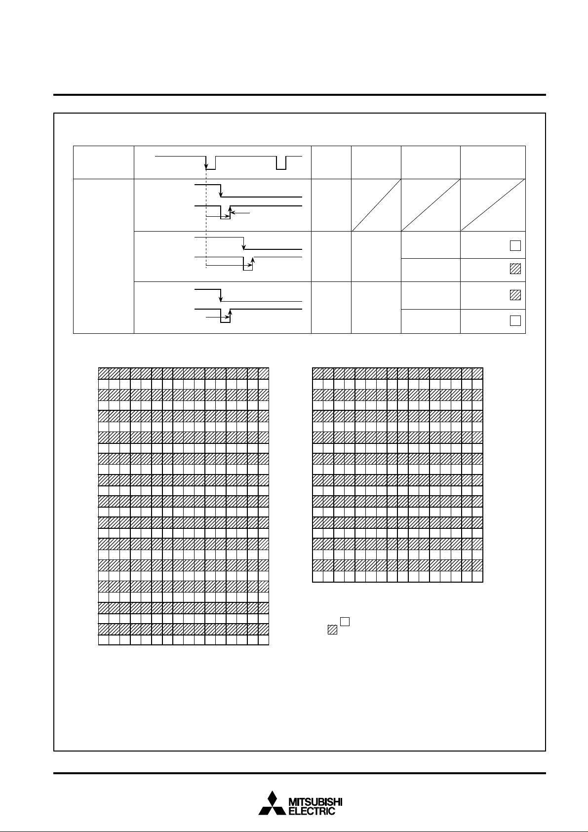
MITSUBISHI MICROCOMPUTERS
M37271MF-XXXSP
M37271EF-XXXSP, M37271EFSP
SINGLE-CHIP 8-BIT CMOS MICROCOMPUTER with CLOSED CAPTION DECODER
Both HSYNC signal and VSYNC signal are negative-polarity input
and ON-SCREEN DISPLAY CONTROLLER
H
SYNC
VSYNC and
SYNC
V
control
signal
in microcomputer
Upper :
SYNC signal
V
Lower :
SYNC control
V
signal in
micro computer
When using the field determination flag, be sure to set bit 0 of the PWM mode register 1 (address 020A
13579111315
1
2
3
4
5
6
7
8
9
10
11
12
13
14
15
16
17
18
19
20
21
22
23
24
25
26
(n–1) field
(Odd-numbered)
T1
(n) field
(Even-numbered)
T2
(n+1) field
(Odd-numbered)
T3
2 4 6 8 10 12 14 16
CC mode · EXOSD mode
0.25 to 0.50[ms] at
f(X
IN) = 8 MHz
Field
Odd
Even
Odd
135791113152 4 6 8 10 12 14 16
1
2
3
4
5
6
7
8
9
10
11
12
13
14
15
16
17
18
19
20
When the display dot line selection bit is “0,”
the “ ” font is displayed at even field, the
“ ” font is displayed at odd field. Bit 7 of the
I/O polarity control register can be read as the
field determination flag : “1” is read at odd field,
“0” is read at even field.
Field
determination
flag(Note)
0 (T2 > T1)
1 (T3 < T2)
Display dot line
selection bit
OSD mode
0
1
0
1
16) to “0.”
Display dot line
Dot line 1
Dot line 0
Dot line 0
Dot line 1
Character ROM font configuration diagram
Note : The field determination flag changes at a rising edge of the V
the microcomputer.
Fig. 65. Relation between field determination flag and display font
SYNC control signal (negative-polarity input) in
57

MITSUBISHI MICROCOMPUTERS
M37271MF-XXXSP
M37271EF-XXXSP, M37271EFSP
SINGLE-CHIP 8-BIT CMOS MICROCOMPUTER with CLOSED CAPTION DECODER
and ON-SCREEN DISPLAY CONTROLLER
(6) Memory for OSD
There are 2 types of memory for OSD : ROM for OSD (addresses
1080016 to 1567F16, 1800016 to 1E43F16) used to store character
dot data (masked) and RAM for OSD (addresses 080016 to 0FFF16)
used to specify the characters and colors to be displayed. The following describes each type of memory.
11
1 ROM for OSD (addresses 1080016 to 1567F16, 1800016 to
11
1E43F16)
The ROM for OSD contains dot pattern data for characters to be
displayed. To actually display the character code and the extra code
stored in this ROM, it is necessary to specify them by writing the
character code inherent to each character (code determined based
on the addresses in the ROM for OSD) into the RAM for OSD.
OSD ROM address of character font data
OSD ROM
address bit
Line number/character
code/font bit
Line number
Character code
Font bit
AD16 AD15 AD14 AD13 AD12 AD11 AD10 AD9 AD8 AD7 AD6 AD5 AD4 AD3 AD2 AD1 AD0
10
16” to “1516”
“02
=
=
16” to “13F16”
“00
=
0 : left font 1 : right font
Line number Character code
The OSD ROM of the character font has a capacity of 12800 bytes.
Since 40 bytes are required for 1 character data, the ROM can stores
up to 320 kinds of characters. The OSD ROM of the extra font has a
capacity of 1664 bytes. Since 52 bytes are required for 1 character
data, the ROM can stores up to 32 kinds of characters.
Data of the character font and extra font is specified shown in Figure
66.
Font
bit
OSD ROM address of extra font data
OSD ROM
address bit
Line number/extra code
/font bit
Line number
Extra code
Font bit
Line
number
02
16
03
16
04
16
05
16
06
16
07
16
08
16
09
16
0A
16
0B
16
0C
16
0D
16
0E
16
0F
16
10
16
11
16
12
16
13
16
14
16
15
16
AD16 AD15 AD14 AD13 AD12 AD11 AD10 AD9 AD8 AD7 AD6 AD5 AD4 AD3 AD2 AD1 AD0
11 0000
=
16” to “1916”
“00
=
16” to “1F16”
“00
=
0 : left font 1 : right font
Left
font
b0b7 b0b7
Character font
Line number
Right
font
Data in
OSD
ROM
0000
16
7FF0
16
7FF8
16
601C
16
600C
16
600C
16
600C
16
600C
16
601C
16
7FF8
16
7FF0
16
6300
16
6380
16
61C0
16
60E0
16
6070
16
6038
16
601C
16
600C
16
0000
16
Line
number
00
01
02
03
04
05
06
07
08
09
0A
0B
0C
0D
00
00
10
11
12
13
14
15
16
17
18
19
b0
Font
Data in
OSD
ROM
FFFE
FFFF
16
0003
16
0003
16
0003
16
0003
16
0003
16
0003
16
0003
16
0003
16
0003
16
0003
16
0003
16
0003
16
0003
16
0003
16
0003
16
0003
16
0003
16
0003
16
0003
16
0003
16
FFFF
16
FFFE
0000
16
0000
16
bit
16
16
Extra code
Left
16
16
16
16
16
16
16
16
16
16
16
16
16
16
16
16
16
16
16
16
16
16
16
16
16
16
font
b0b7
Right
b7
font
Fig. 66. OSD character data storing form
58
Extra font

MITSUBISHI MICROCOMPUTERS
M37271MF-XXXSP
M37271EF-XXXSP, M37271EFSP
SINGLE-CHIP 8-BIT CMOS MICROCOMPUTER with CLOSED CAPTION DECODER
22
2 RAM for OSD (addresses 080016 to 0FFF16)
22
The RAM for OSD is allocated at addresses 080016 to 0FFF16, and
is divided into a display character code specification part, color code
1 specification part, and color code 2 specification part for each block.
Table 14 shows the contents of the RAM for OSD.
For example, to display 1 character position (the left edge) in block
1, write the character code in address 080016, write the color code 1
at 084016, and write the color code 2 at 082816.
The structure of the RAM for OSD is shown in Figure 68.
Table 14. Contents of OSD RAM
Block
Block 1
Block 2
Block 3
Block 4
Block 5
Display position (from left)
1st character
2nd character
:
24th character
25th character
:
39th character
40th character
1st character
2nd character
:
24th character
25th character
:
39th character
40th character
1st character
2nd character
:
24th character
25th character
:
39th character
40th character
1st character
2nd character
:
24th character
25th character
:
39th character
40th character
1st character
2nd character
:
24th character
25th character
:
39th character
40th character
Character code specification
Note: For the OSD mode block with dot size of 1.5TC ✕ 1/2H and
1.5TC ✕ 1H, the 3nth (n = 1 to 13) character is skipped as
compared with ordinary block✽. Accordingly, maximum 26 characters are only displayed in 1 block. The RAM data for the
3nth character does not effect the display. Any character data
can be stored here (refer to Figure 67).
✽ Blocks with dot size of 1TC ✕ 1/2H and 1TC ✕ 1H, or blocks
080016
080116
:
081716
081816
:
082616
082716
088016
088116
:
089716
0E9816
:
08A616
08A716
090016
090116
:
091716
091816
:
092616
092716
098016
098116
:
099716
099816
:
09A616
09A716
0A0016
0A0116
:
0A1716
0A1816
:
0A2616
0A2716
and ON-SCREEN DISPLAY CONTROLLER
on the layer 1
Color code 1 specification
084016
084116
:
085716
085816
:
086616
086716
08C016
08C116
:
08D716
08D816
:
08E616
08E716
094016
094116
:
095716
095816
:
096616
096716
09C016
09C116
:
09D716
08D816
:
09E616
09E716
0A4016
0A4116
:
0A5716
0A5816
:
0A6616
0A6716
Color code 2 specification
082816
082916
:
083F16
086816
:
087616
087716
08A816
08A916
:
08BF16
08E816
:
08F616
08F716
092816
092916
:
093F16
096816
:
097616
097716
09A816
09A916
:
09BF16
09E816
:
09F616
09F716
0A2816
0A2916
:
0A3F16
0A6816
:
0A7616
0A7716
59

MITSUBISHI MICROCOMPUTERS
M37271MF-XXXSP
M37271EF-XXXSP, M37271EFSP
SINGLE-CHIP 8-BIT CMOS MICROCOMPUTER with CLOSED CAPTION DECODER
and ON-SCREEN DISPLAY CONTROLLER
Table 14. Contents of OSD RAM (continued)
Block
Block 6
Block 7
Block 8
Block 9
Block 10
Block 11
Display position (from left)
1st character
2nd character
:
24th character
25th character
:
39th character
40th character
1st character
2nd character
:
24th character
25th character
:
39th character
40th character
1st character
2nd character
:
24th character
25th character
:
39th character
40th character
1st character
2nd character
:
24th character
25th character
:
39th character
40th character
1st character
2nd character
:
24th character
25th character
:
39th character
40th character
1st character
2nd character
:
24th character
25th character
:
39th character
40th character
Character code specification
0A8016
0A8116
:
0A9716
0A9816
:
0AA616
0AA716
0B0016
0B0116
:
0B1716
0B1816
:
0B2616
0B2716
0B8016
0B8116
:
0B9716
0B9816
:
0BA616
0BA716
0C0016
0C0116
:
0C1716
0C1816
:
0C2616
0C2716
0C8016
0C8116
:
0C9716
0C9816
:
0CA616
0CA716
0D0016
0D0116
:
0D1716
0D1816
:
0D2616
0D2716
Color code 1 specification
0AC016
0AC116
:
0AD716
0AD816
:
0AE616
0AE716
0B4016
0B4116
:
0B5716
0B5816
:
0B6616
0B6716
0BC016
0BC116
:
0BD716
0BD816
:
0BE616
0BE716
0C4016
0C4116
:
0C5716
0C5816
:
0C6616
0C6716
0CC016
0CC116
:
0CD716
0CD816
:
0CE616
0CE716
0D4016
0D4116
:
0D5716
0D5816
:
0D6616
0D6716
Color code 2 specification
0AA816
0AA916
:
0ABF16
0AE816
:
0AF616
0AF716
0B2816
0B2916
:
0B3F16
0B6816
:
0B7616
0B7716
0BA816
0BA916
:
0BBF16
0BE816
:
0BF616
0BF716
0C2816
0C2916
:
0C3F16
0C6816
:
0C7616
0C7716
0CA816
0CA916
:
0CBF16
0CE816
:
0CF616
0CF716
0D2816
0D2916
:
0D3F16
0D6816
:
0D7616
0D7716
60

MITSUBISHI MICROCOMPUTERS
M37271MF-XXXSP
M37271EF-XXXSP, M37271EFSP
SINGLE-CHIP 8-BIT CMOS MICROCOMPUTER with CLOSED CAPTION DECODER
Table 14. Contents of OSD RAM (continued)
and ON-SCREEN DISPLAY CONTROLLER
Block
Block 12
Block 13
Block 14
Block 15
Block 16
Display position (from left)
1st character
2nd character
:
24th character
25th character
:
39th character
40th character
1st character
2nd character
:
24th character
25th character
:
39th character
40th character
1st character
2nd character
:
24th character
25th character
:
39th character
40th character
1st character
2nd character
:
24th character
25th character
:
39th character
40th character
1st character
2nd character
:
24th character
25th character
:
39th character
40th character
Character code specification
0D8016
0D8116
:
0D9716
0D9816
:
0DA616
0DA716
0E0016
0E0116
:
0E1716
0E1816
:
0E2616
0E2716
0E8016
0E8116
:
0E9816
0E9916
:
0EA616
0EA716
0F0016
0F0116
:
0F1716
0F1816
:
0F2616
0F2716
0F8016
0F8116
:
0F9716
0F9816
:
0FA616
0FA716
Color code 1 specification
0DC016
0DC116
:
0DD716
0DD816
:
0DE616
0DE716
0E4016
0E4116
:
0E5716
0E5816
:
0E6616
0E6716
0EC016
0EC116
:
0ED716
0ED816
:
0EE616
0EE716
0F4016
0F4116
:
0F5716
0F5816
:
0F6616
0F6716
0FC016
0FC116
:
0FD716
0FD816
:
0FE616
0FE716
Color code 2 specification
0DA816
0DA916
:
0DBF16
0DE816
:
0DF616
0DF716
0E2816
0E2916
:
0E3F16
0E6816
:
0E7616
0E7716
0EA816
0EA916
:
0EBF16
0EE816
:
0EF616
0EF716
0F2816
0F2916
:
0F3F16
0F6816
:
0F7616
0F7716
0FA816
0FA916
:
0FBF16
0FE816
:
0FF616
0FF716
Display
sequence
RAM
address
order
Display
sequence
RAM
address
order
1
1223445576871081191310141116121713191420152216231725182619282029213122322334243525372638
1 2 3 4 5 6 7 8 9 1011 1213 14151617 18 1920 21 2223 2425262728 2930 3132 3334 35 3637 3839 40
1 2 3 4 5 6 7 8 9 10111213141516171819202122232425262728293031323334353637383940
Fig. 67. RAM data for 3nth character
1.5Tc size
block
1Tc size
block
61

MITSUBISHI MICROCOMPUTERS
M37271MF-XXXSP
M37271EF-XXXSP, M37271EFSP
SINGLE-CHIP 8-BIT CMOS MICROCOMPUTER with CLOSED CAPTION DECODER
and ON-SCREEN DISPLAY CONTROLLER
Note: Do not read from and write to addresses in OSD RAM shown
in Table 15.
Table 15. List of access disable addresses
087816
08F816
097816
09F816
0A7816
0AF816
0B7816
0BF816
0C7816
0CF816
0D7816
0DF816
0E7816
0EF816
0F7816
0FF816
087916
08F916
097916
09F916
0A7916
0AF916
0B7916
0BF916
0C7916
0CF916
0D7916
0DF916
0E7916
0EF916
0F7916
0FF916
087A16
08FA16
097A16
09FA16
0A7A16
0AFA16
0B7A16
0BFA16
0C7A16
0CFA16
0D7A16
0DFA16
0E7A16
0EFA16
0F7A16
0FFA16
62

MITSUBISHI MICROCOMPUTERS
M37271MF-XXXSP
M37271EF-XXXSP, M37271EFSP
SINGLE-CHIP 8-BIT CMOS MICROCOMPUTER with CLOSED CAPTION DECODER
Blocks 1 to16
and ON-SCREEN DISPLAY CONTROLLER
RF6 RF5 RF4 RF3 RF2 RF1 RF0 RC17 RC16 RC15 RC14 RC13 RC12 RC11 RC10 RC23 RC22 RC21 RC20RF7
Character code Color code 1 Color code 2
Bit
RF0
RF1
RF2
RF3
RF4
RF5
RF6
RF7
RC10
RC11
RC12
RC13
RC14
RC15
RC16
RC17
RC20
RC21
RC22
RC23
Notes 1: Read value of bits 4 to 7 of the color code 2 is undefined.
Bit name
Character code
(Low-order 8 bits)
Character code
(High-order 1 bit)
Control of
character color R
Control of
character color G
Control of
character color B
OUT1 control
Flash control
Underline control
Italic control
Control of background
color R
Control of background
color G
Control of background
color B
Not used
2: For “not used” bits, the write value is read.
3: The decode value of the extra code is “EX4.”
CC mode OSD mode EXOSD mode
Function
Specification of
character code in
OSD ROM
0: Color signal output OFF
1: Color signal output ON
0:
Character output
1:
Background output
0: Flash OFF
1: Flash ON
0: Underline OFF
1: Underline ON
0: Italic OFF
1: Italic ON
0: Color signal output OFF
1: Color signal output ON
Bit name
Character code
(Low-order 8 bits)
Character code
(High-order 1 bit)
Control of
character color R
Control of
character color G
Control of
character color B
OUT1 control
Control of
character color I1
Not used
Control of background
color R
Control of background
color G
Control of background
color B
Control of background
color
I1
Function
Specification of
character code in
OSD ROM
0: Color signal output OFF
1: Color signal output ON
0:
Character output
1:
Background output
0: Color signal output OFF
1: Color signal output ON
0: Color signal output OFF
1: Color signal output ON
Background color code 0
Background color code 1
Background color code 2
b3b0b7b0b7
Bit name
Character code
(Low-order 8 bits)
Character code
(High-order 1 bit)
Character color code 0
(CC0)
Character color code 1
(CC1)
Character color code 2
(CC2)
OUT1 control
Extra code 0
(EX0)
Extra code 1
(EX1)
Extra code 2
(EX2)
(BCC0)
(BCC1)
(BCC2)
Extra code 3
(EX3)
b0
Function
Specification of
character code in
OSD ROM
Specification of
character color
0:
Character output
1:
Background output
Specification of
extra code in OSD
ROM
Specification of
background color
Specification of
extra code in OSD
ROM
Fig. 68. Structure of OSD RAM
63

MITSUBISHI MICROCOMPUTERS
M37271MF-XXXSP
M37271EF-XXXSP, M37271EFSP
SINGLE-CHIP 8-BIT CMOS MICROCOMPUTER with CLOSED CAPTION DECODER
and ON-SCREEN DISPLAY CONTROLLER
(7) Character color
The color for each character is displayed by the color code 1. The
kinds and specification method of character color are different depending on each mode.
CC mode.................. 7 kinds
•
OSD mode ...............15 kinds
•
EXOSD mode .......... 7 kinds
•
The correspondence Table of the color code 1 and color signal output in the EXOSD mode is shown in Table 16.
Specified by bits 1 (R), 2 (G), and 3 (B) of
the color code 1
Specified by bits 1 (R), 2 (G), 3 (B), and 5
(I1) of the color code 1
Specified by bits 1 (CC0), 2 (CC1), and
3 (CC2) of the color code 1
(8) Character background color
The character background color can be displayed in the character
display area. The character background color for each character is
specified by the color code 2. The kinds and specification method of
character background color are different depending on each mode.
CC mode.................. 7 kinds
•
OSD mode ...............15 kinds
•
EXOSD mode .......... 7 kinds
•
The correspondence table of the color code 2 and color signal output
in the EXOSD mode is shown in Table 17.
Note : The character background color is displayed in the following
part :
(character display area)–(character font)–(border)–(extra font).
Accordingly, the character background color does not mix with
these color signal.
Specified by bits 0 (R), 1 (G), and 2 (B) of
the color code 2
Specified by bits 0 (R), 1 (G), 2 (B), and 3
(I1) of the color code 2
Specified by bits 0 (BCC0), 1 (BCC1), and
2 (BCC2) of the color code 2
Table 16. Correspondence table of color code 1 and color
signal output in EXOSD mode
Color code 1
Bit 3
CC2
Table 17. Correspondence table of color code 2 and color
Bit 2
BCC2
Bit 2
CC1
0
0
0
0
1
1
1
1
signal output in EXOSD mode
Color code 2
Bit 1
BCC1
0
0
0
0
1
1
1
1
Bit 1
CC0
0
0
1
1
0
0
1
1
0
0
1
1
0
0
1
1
0
1
0
1
0
1
0
1
Bit 0
BCC0
0
1
0
1
0
1
0
1
Color signal output
R
G
0
0
1
0
0
1
1
1
1
1
1
1
0
1
1
1
Color signal output
G
R
0
0
0
1
1
0
1
1
1
1
1
1
1
0
1
1
B
I1
0
0
0
0
0
0
0
1
0
0
1
1
1
0
1
0
B
I1
0
0
0
0
0
0
0
1
0
0
1
1
1
0
1
0
I2
0
0
0
0
1
0
0
0
I2
0
0
0
0
1
0
0
0
64

MITSUBISHI MICROCOMPUTERS
M37271MF-XXXSP
M37271EF-XXXSP, M37271EFSP
SINGLE-CHIP 8-BIT CMOS MICROCOMPUTER with CLOSED CAPTION DECODER
and ON-SCREEN DISPLAY CONTROLLER
(9) OUT1, OUT2 signals
The OUT1, OUT2 signals are used to control the luminance of the
video signal. The output waveform of the OUT1, OUT2 signals is
controlled by bit 4 of the color code 1 (refer to Figure 68), bits 2 and
Block control register
OUT2 output
control bit (b7)
Border output
control bit (b2)
OUT1
control
(b4 of color
code 1)
7 of the block control register (refer to Figure 53). The setting values
for controlling OUT1, OUT2 and the corresponding output waveform
is shown in Figure 69.
Output
waveform
0
OUT1
OUT2
0
1
0
0
OUT1
OUT2
OUT1
OUT2
1
1
OUT1
OUT2
0
OUT1
OUT2
0
1
OUT1
OUT2
1
0
OUT1
OUT2
1
OUT1
1
OUT2
Fig. 69. Setting value for controlling OUT1, OUT2 and corresponding output waveform
65

MITSUBISHI MICROCOMPUTERS
M37271MF-XXXSP
M37271EF-XXXSP, M37271EFSP
SINGLE-CHIP 8-BIT CMOS MICROCOMPUTER with CLOSED CAPTION DECODER
and ON-SCREEN DISPLAY CONTROLLER
44
4 Extra font
(10) Attribute
The attributes (flash, underline, italic) are controlled to the character
font. The attributes for each character are specified by the color codes
1 and 2 (refer to Figure 68). The attributes to be controlled are different depending on each mode.
CC mode..................... Flash, underline, italic
OSD mode .................. Border (all bordered, shadow bordered can
be selected)
EXOSD mode ............. Border (all bordered, shadow bordered can
be selected) , extra font (32 kinds)
11
1 Under line
11
The underline is output at the 23th and 24th dots in vertical direction
only in the CC mode. The underline is controlled by bit 6 of the color
code 1. The color of underline is the same color as that of the character font.
22
2 Flash
22
The parts of the character font, the underline, and the character background are flashed only in the CC mode. The color signals (R, G, B,
OUT1) of the character font and the underline are controlled by bit 5
of the color code 1. All of the color signals for the character font flash.
However, the color signal for the character background can be controlled by bit 3 of the OSD control register (refer to Figure 52). The
flash cycle bases on the V
· VSYNC cycle ✕ 48 ; 768 ms (at flash ON)
· VSYNC cycle ✕ 16 ; 256 ms (at flash OFF)
33
3 Italic
33
The italic is made by slanting the font stored in OSD ROM only in the
CC mode. The italic is controlled by bit 7 of the color code 1.
The display example of the italic and underline is shown in Figure 70.
In this case, 16 26 dots are used and “R” is displayed.
Notes 1: When setting both the italic and the flash, the italic charac-
ter flashes.
2: When the pre-divide ratio = 1, the italic character with slant
of 1 dot ✕ 5 steps is displayed (refer to Figure 71 (c)). When
the pre-divide ratio = 2, the italic character with slant of 1/2
dot ✕ 10 steps is displayed (refer to Figure 71 (d)).
3: The boundary of character color is displayed in italic. How-
ever, the boundary of character background color is not affected by the italic (refer to Figure 72).
4: The adjacent character (one side or both side) to an italic
character is displayed in italic even when the character is
not specified to display in italic (refer to Figure 72).
5: When displaying the italic character in the block with the
pre-divide ratio = 1, set the OSD clock frequency to 11 MHz
to 14 MHz.
SYNC count.
44
There are 32 kinds of the extra fonts configured with 16 ✕ 26 dots in
OSD ROM. 16 kinds of these fonts can be displayed by ORed with
the character font by a character unit (refer to Figure 50). For the
others, only the extra font is displayed (refer to Figure 50). In only the
EXOSD mode, the extra font is controlled the following : bits 7 to 5 of
the color code 1, bit 3 of the color code 2, and decode value (EX4) of
the character code. When the character code = “0016” to “13F16,”
EX4 is “0, ” when the character code = “14016,” EX4 is “1.” Since
there is no font with the character code = “14016,” a blank is displayed.
The extra font color for each screen is specified by the extra color
register. When the character font overlaps with the extra font, the
color of the area becomes the ORed color of both fonts.
Note : When using the extra font, set bits 7 and 6 of the OSD control
register to “0” (refer to Figure 52).
7
Fig. 70. Structure of extra font color register
0
Extra font color
register
(EC : address 0218
Extra font color
R control bit
0 : No output
1 : Output
Extra font color
G control bit
0 : No output
1 : Output
Extra font color
B control bit
0 : No output
1 : Output
Extra font color
I1 control bit
0 : No output
1 : Output
Extra font color
I2 control bit
0 : No output
1 : Output
16
)
66

MITSUBISHI MICROCOMPUTERS
M37271MF-XXXSP
M37271EF-XXXSP, M37271EFSP
SINGLE-CHIP 8-BIT CMOS MICROCOMPUTER with CLOSED CAPTION DECODER
and ON-SCREEN DISPLAY CONTROLLER
(a) Ordinary
Color code 1
Bit 6
0
Color code 1
Bit 6 Bit 7
0
Bit 7
0
1
(b) Underline
Color code 1
Bit 6 Bit 7
10
Color code 1
Bit 6
0
Bit 7
1
(c) Italic (pre-divide ratio
= 1)
Fig. 71. Example of attribute display (in CC mode)
Italic on one side
Bit 7 of color
code 1
10 0 1 1 0 1
Note : The wavy-lined is the boundary of character color
Fig. 72. Example of italic display
(d) Italic (pre-divide ratio
Italic on both sides
= 2)
67

MITSUBISHI MICROCOMPUTERS
M37271MF-XXXSP
M37271EF-XXXSP, M37271EFSP
SINGLE-CHIP 8-BIT CMOS MICROCOMPUTER with CLOSED CAPTION DECODER
and ON-SCREEN DISPLAY CONTROLLER
55
5 Border
55
The border is output in the OSD mode and the EXOSD mode. The all
bordered (bordering around of character font) and the shadow bordered (bordering right and bottom sides of character font) are selected (refer to Figure 73) by bit 2 of the OSD control register (refer to
Figure 52). The border ON/OFF is controlled by bit 2 of the block
control register (refer to Figure 53).
The OUT1 signal is used for border output. The border color for each
screen is specified by the border color register.
The horizontal size (x) of border is 1TC (OSD clock cycle divided in
the pre-divide circuit) regardless of the character font dot size. The
vertical size (y) different depending on the screen scan mode and
the vertical dot size of character font.
Notes 1 : There is no border for the extra font.
2 : The border dot area is the shaded area as shown in Figure
75. In the EXOSD mode, top and bottom of character font
display area is not bordered.
3 : When the border dot overlaps on the next character
font, the character font has priority (refer to Figure 76 A).
When the border dot overlaps on the next character back
ground, the border has priority (refer to Figure 76 B).
4 : The border is not displayed at right side of the most right
dot in the display area of the 40th character (the character
located at the most right of the block).
All bordered Shadow bordered
Fig. 73. Example of border display
y
x
Scan mode
Border
dot size
Horizontal size (x)
Vertical size (y)
Fig. 74. Horizontal and vertical size of border
Vertical dot size of
character font
Normal scan mode Bi-scan mode
1/2H 1H, 2H, 3H 1/2H, 1H, 2H, 3H
1T
C
(OSD clock cycle divided in pre-divide circuit)
1/2H 1H 1H
68

MITSUBISHI MICROCOMPUTERS
M37271MF-XXXSP
M37271EF-XXXSP, M37271EFSP
SINGLE-CHIP 8-BIT CMOS MICROCOMPUTER with CLOSED CAPTION DECODER
and ON-SCREEN DISPLAY CONTROLLER
1 dot width of border
Fig. 75. Border area
20 dots
OSD mode
16 dots
1 dot width of border
Character
font area
1 dot width of border
EXOSD mode
16 dots
20 dots
1 dot width of border
Character boundaryBCharacter boundaryACharacter boundary
B
Fig. 76. Border priority
70
Border color register
(FC : address 021B
Border color R control b
0 : No output
1 : Output
Border color G control bit
0 : No output
1 : Output
Border color B control bit
0 : No output
1 : Output
Border color I1 control bit
0 : No output
1 : Output
Border color I2 control bit
0 : No output
1 : Output
Fig. 77. Structure of border color register
16
)
69

MITSUBISHI MICROCOMPUTERS
M37271MF-XXXSP
M37271EF-XXXSP, M37271EFSP
SINGLE-CHIP 8-BIT CMOS MICROCOMPUTER with CLOSED CAPTION DECODER
and ON-SCREEN DISPLAY CONTROLLER
(11) Multiline Display
The M37271MF-XXXSP can ordinarily display 16 lines on the CRT
screen by displaying 16 blocks at different vertical positions. In addition, it can display up to 16 lines by using OSD interrupts.
An OSD interrupt request occurs at the point at which display of each
block has been completed. In other words, when a scanning line
reaches the point of the display position (specified by the vertical
position registers) of a certain block, the character display of that
block starts, and an interrupt occurs at the point at which the scanning line exceeds the block. The mode in which an OSD interrupt
occurs is different depending on the setting of the raster color register (refer to Figure 84).
· When bit 7 of the raster color register is “0”
An OSD interrupt occurs at the end of block display in the OSD
and the EXOSD mode.
· When bit 7 of the raster color register is “1”
An OSD interrupt occurs at the end of block display in the CC mode.
Block 1 (on display)
“OSD interrupt request”
Notes 1: An OSD interrupt does not occur at the end of display when
the block is not displayed. In other words, if a block is set to
off display by the display control bit of the block control register (addresses 00D016 to 00DF16), an OSD interrupt request does not occur (refer to Figure 78 (A)).
2: When another block display appeares while one block is
displayed, an OSD interrupt request occurs only once at
the end of the another block display (refer to Figure 78 (B)).
3: On the screen setting window, an OSD interrupt occurs
even at the end of the CC mode block (off display) out of
window (refer to Figure 78 (C)).
Block 1 (on display)
“OSD interrupt request”
Block 2 (on display)
Block 3 (on display)
Block 4 (on display)
On display (OSD interrupt request occurs
at the end of block display)
Block 1
Block 2
(B) (C)
“OSD interrupt request”
“OSD interrupt request”
“OSD interrupt request”
(A)
No
“OSD interrupt request”
“OSD interrupt request”
Window
Block 2 (on display)
Block 3 (off display)
Block 4 (off display)
Off display (OSD interrupt request does
not occur at the end of block display)
Block 1
Block 2
Block 3
In CC mode
“OSD interrupt request”
No
“OSD interrupt request”
No
“OSD interrupt request”
“OSD interrupt request”
“OSD interrupt request”
“OSD interrupt request”
Fig. 78. Note on occurence of OSD interrupt
70

MITSUBISHI MICROCOMPUTERS
M37271MF-XXXSP
M37271EF-XXXSP, M37271EFSP
SINGLE-CHIP 8-BIT CMOS MICROCOMPUTER with CLOSED CAPTION DECODER
and ON-SCREEN DISPLAY CONTROLLER
(12) Automatic Solid Space Function
This function generates automatically the solid space (OUT1 or OUT2
blank output) of the character area in the CC mode.
The solid space is output in the following area :
· the character area except character code “00916 ”
· the character area on the left and right sides of the character area
except character code “00916 ”
This function is turned on and off by bit 4 of the OSD control register
(refer to Figure 52).
Table 18. Setting for automatic solid space
Bit 4 of OSD control register
Bit 7 of block control register
Bit 4 of color code 1
OUT1 output signal
OUT2 output signal
0
01
Character Character
font part display
area
OFF
0
Notes 1 : Blank is disabled on the left side of the 1st character and
on the right side of the 40th character of each block.
2 : When using this function, set “00916” to the 40th character.
1
01
Character
font part
OFF Character
display
area
1
0
01
Solid
space
OFF
1
01
Character
font part
Solid
space
When setting the character code “00516” as the character A, “00616” as the character B.
(Display memory)
009 005 009 009 009 006 006
16 16 16 16 16 16 16
(Display screen)
Character to be displayed
• • •
006 009
16 16
• • •
1st
(Note 1)
Fig. 79. Display screen example of automatic solid space
character
2nd
character
No blank output
00916009
16
39th
character
40th
character
(Note 2)(Note 1)
71

MITSUBISHI MICROCOMPUTERS
M37271MF-XXXSP
M37271EF-XXXSP, M37271EFSP
SINGLE-CHIP 8-BIT CMOS MICROCOMPUTER with CLOSED CAPTION DECODER
and ON-SCREEN DISPLAY CONTROLLER
(13) Scan Mode
M37271MF-XXXSP has the bi-scan mode for corresponding to HSYNC
of double speed frequency. In the bi-scan mode, the vertical start
display position and the vertical size is two times as compared with
the normal scan mode. The scan mode is selected by bit 1 of the
OSD control register (refer to Figure 52).
Table 19. Setting for scan mode
Parameter
Bit 1 of OSD control register
Vertical display start position
Vertical dot size
Scan mode
Normal scan
0
Value of vertical position register ✕ 1H
1TC ✕ 1/2H
1TC ✕ 1H
2TC ✕ 2H
3TC ✕ 3H
Value of vertical position register ✕ 2H
Bi-scan
1
1TC ✕ 1H
1TC ✕ 2H
2TC ✕ 4H
3TC ✕ 6H
(14) Window Function
This function sets the top and bottom boundary of display limit on a
screen. The window function is valid only in the CC mode. The top
boundary is set by the window H registers 1 and 2. The bottom boundary is set by the window L registers 1 and 2. This function is turned
on and off by bit 5 of the OSD control register (refer to Figure 52).
The structure of the window H registers 1 and 2 is shown in Figure
81, the structure of the window L registers 1 and 2 is shown in Figure
82.
ABCDE
FGHIJ
KLMNO
PQRST
Notes 1: Set values except “0016” and “0116” to the window H regis-
ter 1 when the window H register 2 is “0016.”
2: Set the register value fit for the following condition :
(WH1 + WH2) < (WL1 + WL2)
Top
boundary
EXOSD mode
CC mode
CC mode
CC mode
of window
Window
Fig. 80. Example of window function
72
UVWXY
Screen
OSD mode
Bottom
boundary
of window

MITSUBISHI MICROCOMPUTERS
M37271MF-XXXSP
M37271EF-XXXSP, M37271EFSP
SINGLE-CHIP 8-BIT CMOS MICROCOMPUTER with CLOSED CAPTION DECODER
and ON-SCREEN DISPLAY CONTROLLER
7
7
Note : Set values except “0016” and “0116” to the WH1 when the WH2 is “00
Fig. 81. Structure of window H registers
0
Window H register 1
(WH1 : address 021C
16
)
Control bits of window top boundary (Note)
Top boundary position (low-order 8bits)
H
✕(setting value of low-order 2bits of
T
WH2✕16 +setting value of high-order
4bits of WH1✕16 +setting value of
low-order 4bits of WH1✕16 )
2
1
0
0
Window H register 2
16
(WH2 : address 021E
)
Control bits of window top boundary (Note)
Top boundary position (high-order 2bits)
T
H
✕(setting value of low-order 2bits of
WH2✕16 +setting value of high-order
4bits of WH1✕16 +setting value of
low-order 4bits of WH1✕16 )
2
1
0
16.
”
7
7
Note : Set values fit for the following condition : (WH1+WH2) < (WL1+WL2).
Fig. 82. Structure of window L registers
0
Window L register 1
(WL1 : address 021D
)
16
Control bits of window bottom boundary (Note)
Bottom boundary position (low-order 8bits)
H
✕(setting value of low-order 2bits of
T
WL2✕16 +setting value of high-order
4bits of WL1✕16 +setting value of
low-order 4bits of WL1✕16 )
2
1
0
0
Window L register 2
)
(WL2 : address 021F
16
Control bits of window bottom boundary (Note)
Bottom boundary position (high-order 2bits)
T
H
✕(setting value of low-order 2bits of
WL2✕16 +setting value of high-order
4bits of WL1✕16 +setting value of
low-order 4bits of WL1✕16 )
2
1
0
73

MITSUBISHI MICROCOMPUTERS
M37271MF-XXXSP
M37271EF-XXXSP, M37271EFSP
SINGLE-CHIP 8-BIT CMOS MICROCOMPUTER with CLOSED CAPTION DECODER
and ON-SCREEN DISPLAY CONTROLLER
(15) OSD Output Pin Control
The OSD output pins R, G, B, and OUT1 can also function as ports
P52, P53, P54 and P55. Set the corresponding bit of the OSD port
control register (address 00CB16) to “0” to specify these pins as OSD
output pins, or set it to “1” to specify it as a general-purpose port P5
pins. The OUT2, I1, and I2 can also function as port P10, P15, P16.
Set the corresponding bit of the port P1 direction register (address
00C316) to “1” (output mode). After that, switch between the OSD
output function and the port function by the OSD port control register. Set the corresponding bit to “1” to specify the pin as OSD output
pin, or set it to “0” to specify as port P1 pin.
The input polarity of the HSYNC, VSYNC and output polarity of signals
R, G, B, I1, I2, OUT1 and OUT2 can be specified with the I/O polarity
control register (address 021716) . Set a bit to “0” to specify positive
polarity; set it to “1” to specify negative polarity (refer to Figure 64).
The structure of the OSD port control register is shown in Figure 83.
70
0
OSD port control register
(PF : address 00CB
Port P1
5 output signal selection bit
0 : Port P1
1 : I1 signal output
6 output signal selection bit
Port P1
0 : Port P1
1 : I2 signal output
Port P5
2 output signal selection bit
0 : R signal output
1 : Port P5
Port P5
3 output signal selection bit
0 : G signal output
1 : Port P5
Port P5
4 output signal selection bit
0 : B signal output
1 : Port P5
Port P5
5 output signal selection bit
0 : OUT1 signal output
1 : Port P5
16)
5 output
6 output
2 output
3 output
4 output
5 output
Port P1
0 output signal selection bit
0 : Port P1
1 : OUT2 signal output
Fix this bit to “0.”
0 output
Fig. 83. Structure of OSD port control register
74

A
A
A
A
A
MITSUBISHI MICROCOMPUTERS
M37271MF-XXXSP
M37271EF-XXXSP, M37271EFSP
SINGLE-CHIP 8-BIT CMOS MICROCOMPUTER with CLOSED CAPTION DECODER
(16) Raster Coloring Function
An entire screen (raster) can be colored by setting the bits 6 to 0 of
the raster color register. Since each of the R, G, B, I1, I2, OUT1, and
OUT2 pins can be switched to raster coloring output, 7 raster colors
can be obtained.
If the OUT1 pin has been set to raster coloring output, a raster coloring signal is always output during 1 horizontal scanning period. This
setting is necessary for erasing a background TV image.
If the R, G, B, I1, and I2 pins have been set to output, a raster coloring signal is output in the part except a no-raster colored character
(in Figure 85, a character “1”) during 1 horizontal scanning period.
This ensures that character colors are not mixed with the raster color.
The structure of the raster color register is shown in Figure 84, the
example of raster coloring is shown in Figure 85.
70
and ON-SCREEN DISPLAY CONTROLLER
Raster color register
(RC : address 0218
Raster color R control bit
0 : No output
1 : Output
Raster color G control bit
0 : No output
1 : Output
Raster color B control bit
0 : No output
1 : Output
Raster color I1 control bit
0 : No output
1 : Output
Raster color I2 control bit
0 : No output
1 : Output
Raster color OUT1 control bit
0 : No output
1 : Output
Raster color OUT2 control bit
0 : No output
1 : Output
OSD interrupt source
selection bit
0 : Interrupt occurs at end
of OSD or EXOSD block
display
1 : Interrupt occurs at end
of CC mode block display
16
)
AAAAAAAAA
AAAAAAAAA
A
AAAAAAAAA
AAAAAAAAA
AAAAAAAAA
H
SYNC
OUT1
R
G
B
Fig. 85. Example of raster coloring
Fig. 84. Structure of raster color register
: Character color “RED” (R)
: Border color “GREEN” (G)
: Background color “MAGENTA” (R and B)
: Raster color “BLUE” (R and OUT1)
A'
Signals
across
A-A'
75

MITSUBISHI MICROCOMPUTERS
M37271MF-XXXSP
M37271EF-XXXSP, M37271EFSP
SINGLE-CHIP 8-BIT CMOS MICROCOMPUTER with CLOSED CAPTION DECODER
and ON-SCREEN DISPLAY CONTROLLER
INTERRUPT INTERVAL DETERMINATION
FUNCTION
The M37271MF-XXXSP incorporates an interrupt interval determination circuit. This interrupt interval determination circuit has an 8-bit
binary up counter as shown in Figure 86. Using this counter, it determines an interval or a pulse width on the INT1 or INT2 (refer to Figure 88).
The following describes how the interrupt interval is determined.
1. The determination mode is selected by using bit 5 of the interrupt
interval determination control register (address 021216). When this
bit is set to “0,” the interrupt interval determination mode is selected; when the bit is set to “1,” the pulse width determination
mode is selected.
2. The interrupt input to be determined (INT1 input or INT2 input) is
selected by using bit 2 in the interrupt interval determination control register (address 021216). When this bit is cleared to “0,” the
INT1 input is selected ; when the bit is set to “1,” the INT2 input is
selected.
3. When the INT1 input is to be determined, the polarity is selected
by using bit 3 of the interrupt interval determination control
register ; when the INT2 input is to be determined, the polarity is
selected by using bit 4 of the interrupt interval determination
control register.
When the relevant bit is cleared to “0,” determination is made of
the interval of a positive polarity (rising transition) ; when the bit is
set to “1,” determination is made of the interval of a negative polarity (falling transition).
4. The reference clock is selected by using bit 1 of the interrupt interval determination control register. When the bit is cleared to “0,” a
32µs clock is selected ; when the bit is set to “1,” a 16µs clock is
selected (based on an oscillation frequency of 8MHz in either case).
5. Simultaneously when the input pulse of the specified polarity
(rising or falling transition) occurs on the INT1 pin (or INT2 pin),
the 8-bit binary up counter starts counting up with the selected
reference clock (32µs or 16µs).
6. Simultaneously with the next input pulse, the value of the 8-bit
binary up counter is loaded into the interrupt interval determination register (address 021116) and the counter is immediately reset (“0016”). The reference clock is input in succession even after
the counter is reset, and the counter restarts counting up from
“0016”.
7. When count value “FE16” is reached, the 8-bit binary up counter
stops counting. Then, simultaneously when the next reference
clock is input, the counter sets value “FF16” to the interrupt interval determination register. The reference clock is generated by
setting bit 0 of the PWM mode register 1 to “0.”
76

MITSUBISHI MICROCOMPUTERS
M37271MF-XXXSP
M37271EF-XXXSP, M37271EFSP
SINGLE-CHIP 8-BIT CMOS MICROCOMPUTER with CLOSED CAPTION DECODER
16µs
and ON-SCREEN DISPLAY CONTROLLER
32µs
RE
Control
circuit
1
RE
0
INT2 (Note)
INT1 (Note)
Selection gate :
RE
2
Connected to
black colored
side at rest.
Interrupt interval determination register(8)
RE: Input interval determination control register
Note: The pulse width of external interrupt INT1 and INT2 needs 5 or more machine cycles.
Fig. 86. Block diagram of interrupt interval determination circuit
7
0
Interrupt interval determination
control register
(RE : address 0212
Interrupt interval determination
circuit operation control bit
0 : Stopped
1 : Operating
Reference clock control selection
bit
IN) = 8MHz)
(at f(X
0 : 32µs
1 : 16µs
External interrupt input pin
selection bit
0 : INT1 input
1 : INT2 input
INT1 pin input polarity switch bit
0 : Positive polarity input
1 : Negative polarity input
INT2 pin input polarity switch bit
0 : Positive polarity input
1 : Negative polarity input
Interrupt interval determination mode
switch bit
0 : Interrupt interval determination
mode
1 : Pulse width determination mode
INT3 pin input polarity switch bit
0 : Positive polarity input
1 : Negative polarity input
A-D conversion
source selection bit
0 : INT3 interrupt
1 : A-D conversion interrupt
16)
· INT3 interrupt
8-bit binary up counter (8)
8
(Address 021116)
8
Data bus
INT1 or INT2 input
RE
5
RE
0
0
1
1
RE
i
0
1
0
1
i
:
Bit i (i = 3, 4) of interrupt interval determination
control register (address 021116)
Count interval
Fig. 88. Setting value of interrpt interval determination control
register and measuring interval
Fig. 87. Structure of interrupt interval determination control
register
77

MITSUBISHI MICROCOMPUTERS
M37271MF-XXXSP
M37271EF-XXXSP, M37271EFSP
SINGLE-CHIP 8-BIT CMOS MICROCOMPUTER with CLOSED CAPTION DECODER
and ON-SCREEN DISPLAY CONTROLLER
RESET CIRCUIT
The M37271MF-XXXSP is reset according to the sequence shown
in Figure 90. It starts the program from the address formed by using
the content of address FFFF16 as the high-order address and the
content of the address FFFE16 as the low-order address, when the
______
RESET pin is held at “L” level for 2 µs or more while the power source
voltage is 5 V ± 10 % and the oscillation of a quartz-crystal oscillator
or a ceramic resonator is stable and then returned to “H” level. The
internal state of microcomputer at reset are shown in Figures 3 to 7.
An example of the reset circuit is shown in Figure 89.
The reset input voltage must be kept 0.9 V or less until the power
source voltage surpasses 4.5 V.
Power source voltage 0 V
Reset input voltage 0 V
1
M51953AL
3
Fig. 89. Example of reset circuit
Poweron
5
4
0.1 µF
4.5 V
0.9 V
33
Vcc
36
RESET
32
Vss
M37271MF-XXXSP
X
IN
φ
RESET
Internal RESET
SYNC
Address
Data
Fig. 90. Reset sequence
32768 count of XIN
clock cycle (Note 3)
01, S-1
? ?
01, S
? ? ? ? ?
Notes 1 : f(XIN) and f(φ) are in the relation : f(XIN) = 2·f (φ).
01, S-2
FFFE FFFF
ADH,
AD
L
Reset address from the vector table
ADLAD
H
2 : A question mark (?) indicates an undefined state that
depends on the previous state.
3 : Immediately after a reset, timer 3 and timer 4 are
16
connected in hardware. At this time, “FF
16
in timer 3 and “07
with f(X
IN
)/16, and reset state is released by the timer 4
” is set to timer 4. Timer 3 counts down
” is set
overflow signal.
78

MITSUBISHI MICROCOMPUTERS
M37271MF-XXXSP
M37271EF-XXXSP, M37271EFSP
Ports P0
3, P10, P15–P17, P2, P30, P31
SINGLE-CHIP 8-BIT CMOS MICROCOMPUTER with CLOSED CAPTION DECODER
Direction register
and ON-SCREEN DISPLAY CONTROLLER
CMOS output
Data bus
Ports P0
0–P02, P04–P07
Data bus
Ports P11–P14
Port latch
Direction register
Port latch
Direction register
Ports P03, P10, P15–P17,
P2, P30, P31
Note :Each port is also used as below :
P10 : OUT2
P15 : I1
P16 : I2/INT3
P17 : SIN
P24–P26 : AD3–AD1
N-channel open-drain output
Ports P00–P02, P04–P07
Note :Each port is also used as below :
P00–P02 : PWM4–PWM6
P04–P07 : PWM0–PWM3
N-channel open-drain output
Port P11-P14
Data bus
Fig. 91. I/O pin block diagram (1)
Port latch
Note :Each port is also used as below :
P11 : SCL1
P12 : SCL2
P13 : SDA1
P14 : SDA2
79

MITSUBISHI MICROCOMPUTERS
M37271MF-XXXSP
M37271EF-XXXSP, M37271EFSP
SINGLE-CHIP 8-BIT CMOS MICROCOMPUTER with CLOSED CAPTION DECODER
and ON-SCREEN DISPLAY CONTROLLER
S
OUT
, S
CLK
N-channel open-drain output
Data bus
H
SYNC
Ports P4
, V
SYNC
Internal circuit
0
–P4
4
Direction register
Schmidt input
HSYNC, VSYNC
R, G, B, OUT1
Internal circuit
Ports SOUT, SCLK
Note : Each pin is also used
as below :
SOUT : P45
SCLK : P46
CMOS output
R, G, B, OUT1
Note : Each pin is also used
as below :
R : P52 B : P54
G : P53 OUT1 : P55
Data bus
Fig. 92. I/O pin block diagram (2)
Ports P40–P44
Note : Each port is also used as below :
P40 : AD4
P41 : INT2
P42 : TIM2
P43 : TIM3
P44 : INT1
80

MITSUBISHI MICROCOMPUTERS
M37271MF-XXXSP
M37271EF-XXXSP, M37271EFSP
SINGLE-CHIP 8-BIT CMOS MICROCOMPUTER with CLOSED CAPTION DECODER
and ON-SCREEN DISPLAY CONTROLLER
CLOCK GENERATING CIRCUIT
The M37271MF-XXXSP has 2 built-in oscillation circuits. An oscillation circuit can be formed by connecting a resonator between XIN
and XOUT (XCIN and XCOUT). Use the circuit constants in accordance
with the resonator manufacturer’s recommended values. No external resistor is needed between XIN and XOUT since a feed-back resistor exists on-chip. However, an external feed-back resistor is
needed between XCIN and XCOUT. When using XCIN-XCOUT as subclock, clear bits 5 and 4 of the clock source control register to “0.” To
supply a clock signal externally, input it to the XIN (XCIN) pin and
make the XOUT (XCOUT) pin open. When not using XCIN clock, connect the XCIN to VSS and make the XCOUT pin open.
After reset has completed, the internal clock φ is half the frequency of
XIN. Immediately after poweron, both the XIN and XCIN clock start
oscillating. To set the internal clock φ to low-speed operation mode,
set bit 7 of the CPU mode register (address 00FB16) to “1.”
Oscillation Control
(1) Stop mode
The built-in clock generating circuit is shown in Figure 93. When the
STP instruction is executed, the internal clock φ stops at “H” level. At
the same time, timers 3 and 4 are connected in hardware and “FF16”
is set in the timer 3, “0716” is set in the timer 4. Select f(XIN)/16 or
f(XCIN)/16 as the timer 3 count source (set both bit 0 of the timer
mode register 2 and bit 6 at address 00C716 to “0” before the execution of the STP instruction). And besides, set the timer 3 and timer 4
interrupt enable bits to disabled (“0”) before execution of the STP
instruction. The oscillator restarts when external interrupt is accepted,
however, the internal clock φ keeps its “H” level until timer 4 overflows. Because this allows time for oscillation stabilizing when a ceramic resonator or a quartz-crystal oscillator is used.
(3) Low-Speed Mode
If the internal clock is generated from the sub-clock (XCIN), a low
power consumption operation can be realized by stopping only the
main clock XIN. To stop the main clock, set bit 6 (CM6) of the CPU
mode register (00FB16) to “1.” When the main clock XIN is restarted,
the program must allow enough time to for oscillation to stabilize.
Note that in low-power-consumption mode the XCIN-XCOUT drivability
can be reduced, allowing even lower power consumption (60µA with
f (XCIN) = 32kHz). To reduce the XCIN-XCOUT drivability, clear bit 5
(CM5) of the CPU mode register (00FB16) to “0.” At reset, this bit is
set to “1” and strong drivability is selected to help the oscillation to
start. When an STP instruction is executed, set this bit to “1” by software before executing.
M37271MF-XXXSP
X
CIN
X
COUT
R
f
C
CIN
Fig. 93. Ceramic resonator circuit example
R
C
d
COUT
X
IN
X
OUT
C
IN
C
OUT
(2) Wait mode
When the WIT instruction is executed, the internal clock φ stops in
the “H” level but the oscillator continues running. This wait state is
released at reset or when an interrupt is accepted (Note). Since the
oscillator does not stop, the next instruction can be executed at once.
Note: In the wait mode, the following interrupts are invalid.
(1) VSYNC interrupt
(2) OSD interrupt
(3) Timers 1 and 2 interrupts using P42/TIM2 pin input as count
source
(4) Timer 3 interrupt using P43/TIM3 pin input as count source
(5) Data slicer interrupt
(6) Multi-master I2C-BUS interface interrupt
(7) f(XIN)/4096 interrupt
(8) All timer interrupts using f(XIN)/2 or f(XCIN)/2 as count source
(9) All timer interrupts using f(XIN)/4096 or f(XCIN)/4096 as
count source
(10) A-D conversion interrupt
M37271MF-XXXSP
XCIN
XCOUT XIN XOUT
Open Open
External oscillation
circuit or external
pulse
Vcc
Vss
External oscillation
circuit
Vcc
Vss
Fig. 94. External clock input circuit example
81

MITSUBISHI MICROCOMPUTERS
M37271MF-XXXSP
M37271EF-XXXSP, M37271EFSP
SINGLE-CHIP 8-BIT CMOS MICROCOMPUTER with CLOSED CAPTION DECODER
and ON-SCREEN DISPLAY CONTROLLER
X
CIN
X
COUT
OSC1 oscillating mode
selection bits
IN
(Notes 1, 4)
Main clock (X
Internal system clock
selection bit (Notes 1, 3)
X
OUT
X
“1”
Internal system clock
selection bit (Notes 1, 3)
IN–XOUT
“0”
) stop bit (Notes 1, 3)
1/2
1/8
Timer 3 count
stop bit (Notes 1, 2)
“1”
“0”
Timer 3
count source selection bit (Notes 1, 2)
Timer 3 Timer 4
Timing φ
(Internal clock)
Timer 4 count
stop bit (Notes 1, 2)
SQ
R
STP instruction
Notes 1 : The value at reset is “0.”
2 : Refer to the structure of timer mode register 2.
3 : Refer to the structure of CPU mode register (next page).
4 : Refer to the structure of clock source control register.
WIT
instruction
Fig. 95. Clock generating circuit block diagram
S
R
Reset
Q
Interrupt disable flag I
Interrupt request
Q
S
STP instruction
R
Reset
82

MITSUBISHI MICROCOMPUTERS
M37271MF-XXXSP
M37271EF-XXXSP, M37271EFSP
SINGLE-CHIP 8-BIT CMOS MICROCOMPUTER with CLOSED CAPTION DECODER
and ON-SCREEN DISPLAY CONTROLLER
8MHz oscillating
32kHz oscillating
φ is stopped (“H”)
Timer operating
8MHz oscillating
32kHz oscillating
φ is stopped (“H”)
Timer operating
(Note 3)
WIT instruction
Interrupt
External INT,
timer interrupt,
or SI/O interrupt
WIT instruction
Interrupt
8MHz oscillating
32kHz oscillating
CM7 = 1
6 = 1
CM
Reset
f(φ ) = 4MHz
8MHz oscillating
32kHz oscillating
f(φ ) = 16kHz
High-speed operation
start mode
STP instruction
Interrupt (Note 1)
External INT
CM
7 = 0
STP instruction
Interrupt (Note 2)
6 = 0
CM
The program must
allow time for 8MHz
oscillation to stabilize
8MHz stopped
32kHz stopped
φ is stopped (“H”)
8MHz stopped
32kHz stopped
φ is stopped (“H”)
8MHz stopped
32kHz oscillating
φ is stopped (“H”)
Timer operating
(Note 3)
The example assumes that 8 MHz is being applied to the X IN pin and 32 kHz to the XCIN pin. The φ indicates the internal clock.
Notes 1: When the STP state is ended, a delay of approximately 8ms is automatically generated by timer 3 and timer 4.
2: The delay after the STP state ends is approximately 2s.
3: When the internal clock φ divided by 8 is used as the timer count source, the frequency of the count source is 2kHz.
WIT instruction
Fig. 96. State transitions of system clock
Interrupt
8MHz stopped
32kHz oscillating
f(φ ) = 16kHz
STP instruction
8MHz stopped
32kHz stopped
φ = stopped (“H”)
Interrupt (Note 2)
CPU mode register
(Address : 00FB
CM6 : Main clock (XIN–XOUT) stop bit
0 : Oscillating
1 : Stopped
CM7 : Internal system clock selection bit
0 : X
1 : X
IN-XOUT selected (high-speed mode)
CIN-XCOUT selected (low-speed mode)
16)
83

MITSUBISHI MICROCOMPUTERS
M37271MF-XXXSP
M37271EF-XXXSP, M37271EFSP
SINGLE-CHIP 8-BIT CMOS MICROCOMPUTER with CLOSED CAPTION DECODER
and ON-SCREEN DISPLAY CONTROLLER
DISPLAY OSCILLATION CIRCUIT
The OSD oscillation circuit has a built-in clock oscillation circuits, so
that a clock for OSD can be obtained simply by connecting an LC, a
ceramic resonator, or a quartz-crystal oscillator across the pins OSC1
and OSC2. Which of the sub-clock or the OSD oscillation circuit is
selected by setting bits 5 and 4 of the clock source control register
(address 021616).
OSC2OSC1
L
C1
Fig. 97. Display oscillation circuit
C2
AUTO-CLEAR CIRCUIT
When power source is supplied, the auto-clear function can be performed by connecting the following circuit to the RESET pin.
______
ADDRESSING MODE
The memory access is reinforced with 17 kinds of addressing modes.
Refer to the SERIES 740 <Software> User’s Manual for details.
MACHINE INSTRUCTIONS
There are 71 machine instructions. Refer to the SERIES 740 <Software > User’s Manual for details.
PROGRAMMING NOTES
(1) The divide ratio of the timer is 1/(n+1).
(2) Even though the BBC and BBS instructions are executed imme-
diately after the interrupt request bits are modified (by the program), those instructions are only valid for the contents before
the modification. At least one instruction cycle is needed (such as
an NOP) between the modification of the interrupt request bits
and the execution of the BBC and BBS instructions.
(3) After the ADC and SBC instructions are executed (in decimal
mode), one instruction cycle (such as an NOP) is needed before
the SEC, CLC, or CLD instruction is executed.
(4) An NOP instruction is needed immediately after the execution of
a PLP instruction.
(5) In order to avoid noise and latch-up, connect a bypass capacitor
(≈ 0.1 µF) directly between the VCC pin–VSS pin, AVCC pin–VSS
pin, and the VCC pin–CNVSS pin using a thick wire.
Circuit example 1
RESET
Circuit example 2
RESET
Note : Make the level change from “L” to “H” at the point at
which the power source voltage exceeds the specified
voltage.
Fig. 98. Auto-clear circuit example
Vcc
Vss
Vcc
Vss
84

MITSUBISHI MICROCOMPUTERS
M37271MF-XXXSP
M37271EF-XXXSP, M37271EFSP
SINGLE-CHIP 8-BIT CMOS MICROCOMPUTER with CLOSED CAPTION DECODER
and ON-SCREEN DISPLAY CONTROLLER
DATA REQUIRED FOR MASK ORDERS
The following are necessary when ordering a mask ROM production:
(1) Mask ROM Order Confirmation Form
(2) Mark Specification Form
(3) Data to be written to ROM, in EPROM form (32-pin DIP Type
27C101, three identical copies)
PROM Programming Method
The built-in PROM of the One Time PROM version (blank) and builtin EPROM version can be read or programmed with a general-purpose PROM programmer using a special programming adapter.
Product
M37271EFSP
The PROM of the One Time PROM version (blank) is not tested or
screened in the assembly process and following processes. To ensure proper operation after programming, the procedure shown in
Figure 99 is recommended to verify programming.
PROM programmer
Screening (Caution)
(150°C for 40 hours)
PROM programmer
Name of Programming Adapter
PCA7400
Programming with
Verification with
Functional check in target device
Caution : The screening temperature is far higher
than the storage temperature. Never
expose to 150°C exceeding 100 hours.
Fig. 99. Programming and testing of One Time PROM version
85

MITSUBISHI MICROCOMPUTERS
M37271MF-XXXSP
M37271EF-XXXSP, M37271EFSP
SINGLE-CHIP 8-BIT CMOS MICROCOMPUTER with CLOSED CAPTION DECODER
and ON-SCREEN DISPLAY CONTROLLER
ABSOLUTE MAXIMUM RATINGS
Symbol
VCC, AVCC
VI
VI
VO
VO
IOH
IOL1
IOL2
IOL3
IOL4
Pd
Topr
Tstg
Parameter
Power source voltageVCC, AVCC
Input voltage CNVSS
Input voltage P00–P07, P10–P17, P20–P27,
Output voltage P03, P10–P17, P20–P27, P30,
Output voltage P00–P02, P04–P07
Circuit current R, G, B, OUT1, OUT2, P03,
Circuit current R, G, B, OUT1, OUT2, P03,
Circuit current P11–P14
Circuit current P00–P02, P04–P07
Circuit current P30, P31
Power dissipation
Operating temperature
Storage temperature
P30, P31, P40–P46, P64, OSC1,
XIN, HSYNC, VSYNC, RESET,
CVIN
P31, R, G, B, OUT1, SOUT, SCLK,
XOUT,
OSC2
P15–P17, P20–P27, P30, P31
P15–P17, P20–P27, SOUT, SCLK
______
Conditions
All voltages are based
on VSS.
Output transistors are
cut off.
Ta = 25 °C
Ratings
–0.3 to 6
–0.3 to 6
–0.3 to VCC + 0.3
–0.3 to VCC + 0.3
–0.3 to 13
0 to 1 (Note 1)
0 to 2 (Note 2)
0 to 6 (Note 2)
0 to 1 (Note 2)
0 to 10 (Note 3)
550
–10 to 70
–40 to 125
Unit
V
V
V
V
V
mA
mA
mA
mA
mA
mW
°C
°C
RECOMMENDED OPERATING CONDITIONS (Ta = –10 °C to 70 °C, VCC = 5 V ± 10 %, unless otherwise noted)
29
Limits
Typ.
5.0
0
0
0
0
8.0
32
27.0
15.734
2.0
Max.
5.5
5.5
0
VCC
VCC
0.4 VCC
0.3 VCC
0.2 VCC
10
8.1
35
27.0
27.5
100
400
16.206
2.5
Symbol Parameter
VCC, AVCC
VCC, AVCC
VSS
VIH1
VIH2
VIL1
VIL2
VIL3
IOH
IOL1
IOL2
IOL3
IOL4
fCPU
fCLK
fOSD
fhs1
fhs2
fhs3
fhs4
VI
Power source voltage (Note 4), During CPU, OSD, data slicer operation
RAM hold voltage (when clock is stopped)
Power source voltage
“H” input voltage P00–P07, P10–P17, P20–P27, P30, P31,
“H” input voltage P11–P14 (When using I2C-BUS)
“L” input voltage P00–P07, P10–P17, P20–P27, P30, P31,
“L” input voltage
“L” input voltage (Note 6) P41–P44, P46, P16, P17, HSYNC, VSYNC,
“H” average output current (Note 1) R, G, B, OUT1, OUT2, P03, P15–P17,
“L” average output current (Note 2) R, G, B, OUT1, OUT2, P03, P15–P17,
“L” average output current (Note 2) P11–P14
“L” average output current (Note 2) P00–P02, P04–P07
“L” average output current (Note 3) P30, P31
Oscillation frequency (for CPU operation) (Note 5) XIN
Oscillation frequency (for sub-clock operation) XCIN
Oscillation frequency (for OSD) OSC1
Input frequency TIM2, TIM3, INT1, INT2, INT3
Input frequency SCLK
Input frequency SCL1, SCL2
Input frequency Horizontal sync. signal of video signal
Input amplitude video signal CVIN
P40–P46, P64, HSYNC, VSYNC, RESET,
XIN, OSC1
P40–P46, P63, P64
SCL1, SCL2, SDA1, SDA2, (When using I2C-BUS)
______
RESET, XIN, OSC1
P20–P27, P30, P31
P20–P27, SOUT, SCLK
______
LC oscillating mode
Ceramic oscillating mode
Min.
4.5
2.0
0.8VCC
0.7VCC
7.9
11.0
26.5
15.262
1.5
Unit
V
V
V
0
V
V
V
V
V
mA
1
mA
2
mA
6
mA
1
mA
MHz
kHz
MHz
kHz
MHz
1
kHz
kHz
V
86

MITSUBISHI MICROCOMPUTERS
M37271MF-XXXSP
M37271EF-XXXSP, M37271EFSP
SINGLE-CHIP 8-BIT CMOS MICROCOMPUTER with CLOSED CAPTION DECODER
ELECTRIC CHARACTERISTICS (VCC = 5 V ± 10 %, VSS = 0 V, f(XIN) = 8 MHz, Ta = –10 °C to 70 °C, unless otherwise noted)
Symbol
ICC
VOH
VOL
VT+–VT–
IIZH
IIZL
IIZH
RBS
Notes 1: The total current that flows out of the IC must be 20 or less.
Power source current
“H” output voltage R, G, B, OUT1, OUT2, P03,
“L” output voltage R, G, B, OUT1, OUT2, SOUT,
“L” output voltage P30, P31
“L” output voltage P11–P14
Hysteresis
Hysteresis (Note 6) HSYNC, VSYNC, P41–P44,
“H” input leak current
“L” input leak current
“H” input leak current P00–P02, P04–P07
I2C-BUS·BUS switch connection resistor
(between SCL1 and SCL2, SDA1 and SDA2)
2: The total input current to IC (IOL1 + IOL2 + IOL3) must be 20 mA or less.
3: The total average input current for ports P30, P31 to IC must be 10 mA or less.
4: Connect 0.1 µF or more capacitor externally across the power source pins VCC–VSS and AVCC–VSS so as to reduce power source
noise.
Also connect 0.1 µF or more capacitor externally across the pins VCC–CNVSS.
5: Use a quartz-crystal oscillator or a ceramic resonator for the CPU oscillation circuit. When using the data slicer, use 8 MHz.
6: P16, P41–P44 have the hysteresis when these pins are used as interrupt input pins or timer input pins. P11–P14 have the hysteresis
when these pins are used as multi-master I2C-BUS interface ports. P17 and P46 have the hysteresis when these pins are used as
serial I/O pins.
7: When using the sub-clock, set fCLK < fCPU/3.
Parameter
System operation
Wait mode
Stop mode
P15–P17, P20–P27, P30, P31
SCLK, P00–P07, P15–P17,
P20–P27
______
RESET
P46, P11–P14, P17
______
RESET, P03, P10–P17,
P20–P27, P30, P31, P40–P46,
P63, P64, HSYNC, VSYNC
______
RESET, P00–P07, P10–P17,
P20–P27, P30, P31, P40–P46,
P63, P64, HSYNC, VSYNC
Test conditions
VCC = 5.5 V,
f(XIN) = 8 MHz
VCC = 5.5 V, f(XIN) = 0,
f(XCIN) = 32kHz,
OSD OFF, Data slicer OFF,
Low-power dissipation
mode set (CM5 = “0”,
CM6 = “1”)
VCC = 5.5 V, f(XIN) = 8 MHz
VCC = 5.5 V, f(XIN) = 0,
f(XCIN) = 32kHz,
Low-power dissipation
mode set (CM5 = “0”,
CM6 = “1”)
VCC = 5.5 V, f(XIN) = 0,
f(XCIN) = 0
VCC = 4.5 V
IOH = –0.5 mA
VCC = 4.5 V
IOL = 0.5 mA
VCC = 4.5 V
IOL = 10.0 mA
VCC = 4.5 V IOL = 3 mA
VCC = 5.0 V
VCC = 5.0 V
VCC = 5.5 V
VI = 5.5 V
VCC = 5.5 V
VI = 0 V
VCC = 5.5 V
VI = 12 V
VCC = 4.5 V
and ON-SCREEN DISPLAY CONTROLLER
Limits
Min.
CRT OFF
Data slicer OFF
CRT ON
Data slicer ON
2.4
IOL = 6 mA
Typ.
15
30
60
2
25
1
0.5
0.5
Max.
30
45
200
4
100
10
0.4
3.0
0.4
0.6
0.7
1.3
5
5
10
130
Unit
mA
mA
mA
µA
V
V
V
µA
µA
µA
Ω
87

MITSUBISHI MICROCOMPUTERS
M37271MF-XXXSP
M37271EF-XXXSP, M37271EFSP
SINGLE-CHIP 8-BIT CMOS MICROCOMPUTER with CLOSED CAPTION DECODER
and ON-SCREEN DISPLAY CONTROLLER
A-D CONVERTER CHARACTERISTICS
(VCC = 5 V ± 10 %, VSS = 0 V, f(XIN) = 8 MHz, Ta = –10 °C to 70 °C, unless otherwise noted)
Symbol
—
—
—
VOT
VFST
TCONV
VREF
RLADDER
VIA
Parameter
Resolution
Non-linearity error
Differential non-linearity error
Zero transition error
Full-scale transition error
Conversion time
Reference voltage
Ladder resistor
Analog input current
VCC = 5.12V
IOL (SUM) = 0mA
VCC = 5.12V
Min.
0
0
0
0
12.25
0
Limits
Typ.
25
Max.
±2
±0.9
12.5
VCC
VREF
UnitTest conditions
8
bits
LSB
LSB
2
LSB
4
LSB
µs
V
kΩ
V
MULTI-MASTER I2C-BUS BUS LINE CHARACTERISTICS
Symbol
tBUF
tHD:STA
tLOW
tR
tHD:DAT
tHIGH
tF
tSU:DAT
tSU:STA
tSU:STO
Note: Cb = total capacitance of 1 bus line
Bus free time
Hold time for START condition
“L” period of SCL clock
Rising time of both SCL and SDA signals
Data hold time
“H” period of SCL clock
Falling time of both SCL and SDA signals
Data set-up time
Set-up time for repeated START condition
Set-up time for STOP condition
SDA
tBUF
Parameter
Standard clock mode High-speed clock mode
tHD:STA
Max.
1000
300
Min.
1.3
0.6
1.3
20+0.1Cb
0
0.6
20+0.1Cb
100
0.6
0.6
tSU:STO
Max.
300
0.9
300
Min.
4.7
4.0
4.7
0
4.0
250
4.7
4.0
Unit
µs
µs
µs
ns
µs
µs
ns
ns
µs
µs
tLOW
p
SCL
Fig. 100. Definition diagram of timing on multi-master I2C-BUS
88
S
tHD:STA
tR
tHD:DAT tHIGH
tF
tSU:DAT tSU:STA
Sr
p

MITSUBISHI MICROCOMPUTERS
M37271MF-XXXSP
M37271EF-XXXSP, M37271EFSP
SINGLE-CHIP 8-BIT CMOS MICROCOMPUTER with CLOSED CAPTION DECODER
PACKAGE OUTLINE
and ON-SCREEN DISPLAY CONTROLLER
89

MITSUBISHI MICROCOMPUTERS
M37271MF-XXXSP
M37271EF-XXXSP, M37271EFSP
SINGLE-CHIP 8-BIT CMOS MICROCOMPUTER with CLOSED CAPTION DECODER
and ON-SCREEN DISPLAY CONTROLLER
GZZ–SH10–44B < 5ZA0 >
740 FAMILY MASK ROM CONFIRMATION FORM
Mask ROM number
SINGLE-CHIP MICROCOMPUTER M37271MF-XXXSP
MITSUBISHI ELECTRIC
Note : Please fill in all items marked *.
Company
name
Customer
*
Date
issued
Date :
* 1. Confirmation
Specify the name of the product being ordered and the type of EPROMs submitted.
Three EPROMs are required for each pattern.
If at least two of the three sets of EPROMs submitted contain identical data, we will produce masks based on
this data. We shall assume the responsibility for errors only if the mask ROM data on the products we produce
differs from this data. Thus, extreme care must be taken to verify the data in the submitted EPROMs.
TEL
( )
Date :
Section head
signature
Receipt
Submitted by Supervisor
Issuance
signature
Supervisor
signature
Checksum code for entire EPROM
EPROM type (indicate the type used)
27C101
EPROM address
00000
16
Product name
ASCII code :
0000F
01000
0FFFF
10800
1E43F
Set “FF16” in the shaded area.
(1)
Write the ASCII codes that indicates the product name of “M37271MF–” to addresses 0000
(2)
EPROM data check item (Refer the EPROM data and check “ ” in the appropriate box)
Do you set “FF
●
●
Do you write the ASCII codes that indicates the product
name of “M37271MF–” to addresses 0000
‘M37271MF –’
16
16
ROM 60K bytes
16
16
16
data
OSD ROM
16
” in the shaded area ?
16
to 000F
16
→ Yes
→ Yes
?
(hexadecimal notation)
16
to 000F16.
* 2. Mark specification
Mark specification must be submitted using the correct form for the type package being ordered fill out the appropriate
mark specification form (52P4B for M37271MF-XXXSP) and attach to the mask ROM confirmation form.
90

MITSUBISHI MICROCOMPUTERS
M37271MF-XXXSP
M37271EF-XXXSP, M37271EFSP
SINGLE-CHIP 8-BIT CMOS MICROCOMPUTER with CLOSED CAPTION DECODER
GZZ–SH10–44B < 5ZA0 >
740 FAMILY MASK ROM CONFIRMATION FORM
SINGLE-CHIP MICROCOMPUTER M37271MF-XXXSP
MITSUBISHI ELECTRIC
Writing the product name and character ROM data onto EPROMs
and ON-SCREEN DISPLAY CONTROLLER
Addresses 00000
16 to 0000F16 store the product name, and addresses 10800 16 to 1E43F16 store the character pattern.
If the name of the product contained in the EPROMs does not match the name on the mask ROM confirmation form, the
ROM processing is disabled. Write the data correctly.
1.
Inputting the name of the product with the ASCII code
ASCII codes ‘M37271MF-’ are listed on the right.
The addresses and data are in hexadecimal notation.
Inputting the character ROM
2.
Address
0000
000116
000216
000316
000416
000516
000616
000716
16
=
‘M’
4D
‘3’=33
=
3
‘7’
=
‘2’
3
‘7’=37
=
3
‘1’
‘M’=4D
‘F’=46
7
2
1
16
16
16
16
16
16
16
16
Address
0008
000916
000A16
000B16
000C16
000D16
000E16
000F16
=
‘–’
16
2D
FF
FF
FF
FF
FF
FF
FF
16
16
16
16
16
16
16
16
Input the character ROM data to character ROM. For the character ROM data, see the next page and on.
91

MITSUBISHI MICROCOMPUTERS
M37271MF-XXXSP
M37271EF-XXXSP, M37271EFSP
SINGLE-CHIP 8-BIT CMOS MICROCOMPUTER with CLOSED CAPTION DECODER
and ON-SCREEN DISPLAY CONTROLLER
GZZ–SH10–44B < 5ZA0 >
740 FAMILY MASK ROM CONFIRMATION FORM
SINGLE-CHIP MICROCOMPUTER M37271MF-XXXSP
MITSUBISHI ELECTRIC
Font data must be stored in the proper OSD ROM address according to the following table.
(1)OSD ROM address of character font data
OSD ROM address bit
Line number / Character
code / Font bit
Line number = 02
Character code = 0016 to 13F
Font bit = 0 : Left font
1 : Right font
AD16 AD15 AD14AD13 AD12 AD11 AD10 AD9 AD8 AD7 AD6 AD5 AD4 AD3 AD2 AD1 AD0
16
to 15
10
16
16
Line number Character code
Font
bit
Example) The font data “60” (shaded area ) of the character code “AA16” is stored in address
2
1 0 0 1 0 1 0 0 1 0 1 0 1 0 1 0 0
=1295416.
(2)OSD ROM address of extra font data
OSD ROM address bit
Line number / Extra code /
Font bit
Line number = 0016 to 19
Extra code = 0016 to 1F
AD16 AD15 AD14AD13 AD12 AD11 AD10 AD9 AD8 AD7 AD6 AD5 AD4 AD3 AD2 AD1 AD0
11
16
16
Line number Extra code
0000
Font bit = 0 : Left font
1 : Right font
Example) The font data “03” (shaded area ) of the extra code “0A16” is stored in address
2
1 1 0 0 1 0 1 0 0 0 0 0 1 0 1 0 1
Left font Right font
DB7DB6DB5DB4 DB3 DB2DB1DB0DB7 DB6 DB5 DB4DB3DB2 DB1 DB0
02
Line number
03
04
05
06
07
08
09
0A
0B
0C
0D
0E
0F
10
11
12
13
14
15
16
16
16
16
16
16
16
16
16
16
16
16
16
16
16
16
16
16
16
16
(1) Character code “AA16”
=1941516.
Line number
Left font Right font
DB7 DB6 DB5DB4 DB3 DB2 DB1 DB0DB7 DB6 DB5 DB4 DB3DB2 DB1 DB0
00
16
01
16
02
16
03
16
04
16
05
16
06
16
07
16
08
16
09
16
0A
16
0B
16
0C
16
0D
16
00
16
00
16
10
16
11
16
12
16
13
16
14
16
15
16
16
16
17
16
18
16
16
19
(2) Extra code “0A16”
Font
bit
92
(3/4)

MITSUBISHI MICROCOMPUTERS
M37271MF-XXXSP
M37271EF-XXXSP, M37271EFSP
SINGLE-CHIP 8-BIT CMOS MICROCOMPUTER with CLOSED CAPTION DECODER
GZZ–SH10–44B < 5ZA0 >
740 FAMILY MASK ROM CONFIRMATION FORM
SINGLE-CHIP MICROCOMPUTER M37271MF-XXXSP
MITSUBISHI ELECTRIC
The following OSD ROM addresses must be set “FF.” There are no font data in these addresses.
and ON-SCREEN DISPLAY CONTROLLER
10A8016 to 10BFF16
10E8016 to 10FFF16
1128016 to 113FF16
1168016 to 117FF16
11A8016 to 11BFF16
11E8016 to 11FFF16
1228016 to 123FF16
1268016 to 127FF16
12A8016 to 12BFF16
12E8016 to 12FFF16
1328016 to 133FF16
1368016 to 137FF16
13A8016 to 13BFF16
13E8016 to 13FFF16
1428016 to 143FF16
1468016 to 147FF16
14A8016 to 14BFF16
14E8016 to 14FFF16
1528016 to 153FF16
1568016 to 17FFF16
1804016 to 183FF16
1844016 to 187FF16
1884016 to 18BFF16
18C4016 to 18FFF16
1904016 to 193FF16
1944016 to 197FF16
1984016 to 19BFF16
19C4016 to 19FFF16
1A04016 to 1A3FF16
1A44016 to 1A7FF16
1A84016 to 1ABFF16
1AC4016 to 1AFFF16
1B04016 to 1B3FF16
1B44016 to 1B7FF16
1B84016 to 1BBFF16
1BC4016 to 1BFFF16
1C04016 to 1C3FF16
1C44016 to 1C7FF16
1C84016 to 1CBFF16
1CC4016 to 1CFFF16
1D04016 to 1D3FF16
1D44016 to 1D7FF16
1D84016 to 1DBFF16
1DC4016 to 1DFFF16
1E04016 to 1E3FF16
93

MITSUBISHI MICROCOMPUTERS
M37271MF-XXXSP
M37271EF-XXXSP, M37271EFSP
SINGLE-CHIP 8-BIT CMOS MICROCOMPUTER with CLOSED CAPTION DECODER
and ON-SCREEN DISPLAY CONTROLLER
52P4B (52-PIN SHRINK DIP) MARK SPECIFICATION FORM
94

MITSUBISHI MICROCOMPUTERS
M37271MF-XXXSP
M37271EF-XXXSP, M37271EFSP
SINGLE-CHIP 8-BIT CMOS MICROCOMPUTER with CLOSED CAPTION DECODER
SHRINK DIP MARK SPECIFICATION FORM
for one time PROM version microcomputers
and ON-SCREEN DISPLAY CONTROLLER
95

Keep safety first in your circuit designs!
• Mitsubishi Electric Corporation puts the maximum effort into making semiconductor products better and more reliable, but there is always the possibility that trouble may occur with them. Trouble with
semiconductors may lead to personal injury, fire or property damage. Remember to give due consideration to safety when making your circuit designs, with appropriate measures such as (i) placement of
substitutive, auxiliary circuits, (ii) use of non-flammable material or (iii) prevention against any malfunction or mishap.
Notes regarding these materials
• These materials are intended as a reference to assist our customers in the selection of the Mitsubishi semiconductor product best suited to the customer’s application; they do not convey any license under any
intellectual property rights, or any other rights, belonging to Mitsubishi Electric Corporation or a third party.
• Mitsubishi Electric Corporation assumes no responsibility for any damage, or infringement of any third-party’s rights, originating in the use of any product data, diagrams, charts or circuit application examples
contained in these materials.
• All information contained in these materials, including product data, diagrams and charts, represent information on products at the time of publication of these materials, and are subject to change by Mitsubishi
Electric Corporation without notice due to product improvements or other reasons. It is therefore recommended that customers contact Mitsubishi Electric Corporation or an authorized Mitsubishi Semiconductor
product distributor for the latest product information before purchasing a product listed herein.
• Mitsubishi Electric Corporation semiconductors are not designed or manufactured for use in a device or system that is used under circumstances in which human life is potentially at stake. Please contact
Mitsubishi Electric Corporation or an authorized Mitsubishi Semiconductor product distributor when considering the use of a product contained herein for any specific purposes, such as apparatus or systems for
transportation, vehicular, medical, aerospace, nuclear, or undersea repeater use.
• The prior written approval of Mitsubishi Electric Corporation is necessary to reprint or reproduce in whole or in part these materials.
• If these products or technologies are subject to the Japanese export control restrictions, they must be exported under a license from the Japanese government and cannot be imported into a country other than the
approved destination.
Any diversion or reexport contrary to the export control laws and regulations of Japan and/or the country of destination is prohibited.
• Please contact Mitsubishi Electric Corporation or an authorized Mitsubishi Semiconductor product distributor for further details on these materials or the products contained therein.
© 1997 MITSUBISHI ELECTRIC CORP.
New publication, effective Nov. 1997.
Specifications subject to change without notice.

REVISION DESCRIPTION LIST
M37271MF-XXXSP
M37271EF-XXXSP, M37271EFSP DATA SHEET
Rev. Rev.
No. date
1.0 First Edition 9708
2.0 Information about copyright note, revision number, release date added (last page). 971130
Revision Description
(1/1)
 Loading...