

Datasheet M37207MF-XXXSP, M37207MF-XXXFP, M37207M8-XXXSP, M37207EFSP, M37207EFFP Datasheet (Mitsubishi)
Page 1

MITSUBISHI MICROCOMPUTERS
M37207MF-XXXSP/FP, M37207M8-XXXSP
M37207EFSP/FP
SINGLE-CHIP 8-BIT CMOS MICROCOMPUTER for VOLTAGE SYNTHESIZER
and ON-SCREEN DISPLAY CONTROLLER
DESCRIPTION
The M37207MF-XXXSP/FP and M37207M8-XXXSP are single-chip
microcomputers designed with CMOS silicon gate technology. It is
housed in a 64-pin shrink plastic molded DIP or a 80-pin plastic molded
QFP.
In addition to their simple instruction sets, the ROM, RAM and I/O
addresses are placed on the same memory map to enable easy programming.
The M37207MF-XXXSP/FP has a PWM function and an OSD function, so it is useful for a channel selection system for TV. The features of the M37207EFSP/FP are similar to those of the M37207MFXXXSP/FP except that these chips have a built-in PROM which can
be written electrically. The difference between M37207MF-XXXSP/
FP and M37207M8-XXXSP are the ROM size, RAM size, ROM size
for display and kinds of character. Accordingly, the following descriptions will be for the M37207MF-XXXSP/FP unless otherwise noted.
FEATURES
Number of basic instructions .................................................... 71
•
Memory size .................................................................................
•
Minimum instruction execution time
•
........................................ 0.5 µs (at 8 MHz oscillation frequency)
Power source voltage.................................................. 5 V ± 10 %
•
Subroutine nesting ............................................128 levels (Max.)
•
Interrupts ...................................................... 15 types, 14 vectors
•
8-bit timers ................................................................................. 6
•
Programmable I/O ports
•
(Ports P0, P1, P2, P30–P36, P4, P6) ....................................... 47
Input ports (Ports P70, P71) ....................................................... 2
•
Output ports (Ports P52–P56)..................................................... 5
•
12 V withstand ports................................................................. 10
•
LED drive ports .......................................................................... 4
•
Serial I/O ....................................... 8-bit ✕ 1 channel (2 systems)
•
ROM ......................32K bytes (M37207M8-XXXSP)
62K bytes (M37207MF-XXXSP/FP,
M37207EFSP/FP)
RAM ...................... 512 bytes (M37207M8-XXXSP)
960 bytes (M37207MF-XXXSP/FP,
M37207EFSP/FP)
ROM correction memory ............................ 64 bytes
ROM for display.......8K bytes (M37207M8-XXXSP)
12K bytes (M37207MF-XXXSP/FP,
M37207EFSP/FP)
RAM for display ........................................144 bytes
Multi-master I2C-BUS interface ...............................1 (3 systems)
•
Power dissipation
•
In high-speed mode ........................................................165 mW
CC = 5.5 V, 8 MHz oscillation frequency, CRT on)
(at V
In low-speed mode.........................................................0.33 mW
(at V
CC = 5.5 V, 32 kHz oscillation frequency)
A-D comparator (6-bit resolution)................................8 channels
•
PWM output circuit ...................................... 14-bit ✕ 1, 8-bit ✕ 10
•
Interrupt interval determination circuit ........................................ 1
•
ROM correction function ..........................................32 bytes ✕ 2
•
CRT display function
•
Number of display characters ............... 24 characters ✕ 3 lines
(16 lines maximum)
Kinds of characters .................. 256 kinds (M37207M8-XXXSP)
384 kinds (M37207MF-XXXSP/FP,
M37207EFSP/FP)
Character display area ..........................................12 ✕ 16 dots
Kinds of character sizes .................................................4 kinds
Kinds of character colors (It can be specified by the character)
maximum 15 kinds (R, G, B, I)
Kinds of character background colors (It can be specified by the character)
maximum 7 kinds (R, G, B)
1/2-character unit color specification is possible.
Kinds of raster colors (maximum 15 kinds)
Display position
Horizontal .................................................................. 64 levels
Vertical ....................................................................128 levels
Bordering (horizontal and vertical)
Wipe function
Scanning line double count mode display is possible.
APPLICATION
TV
Page 2
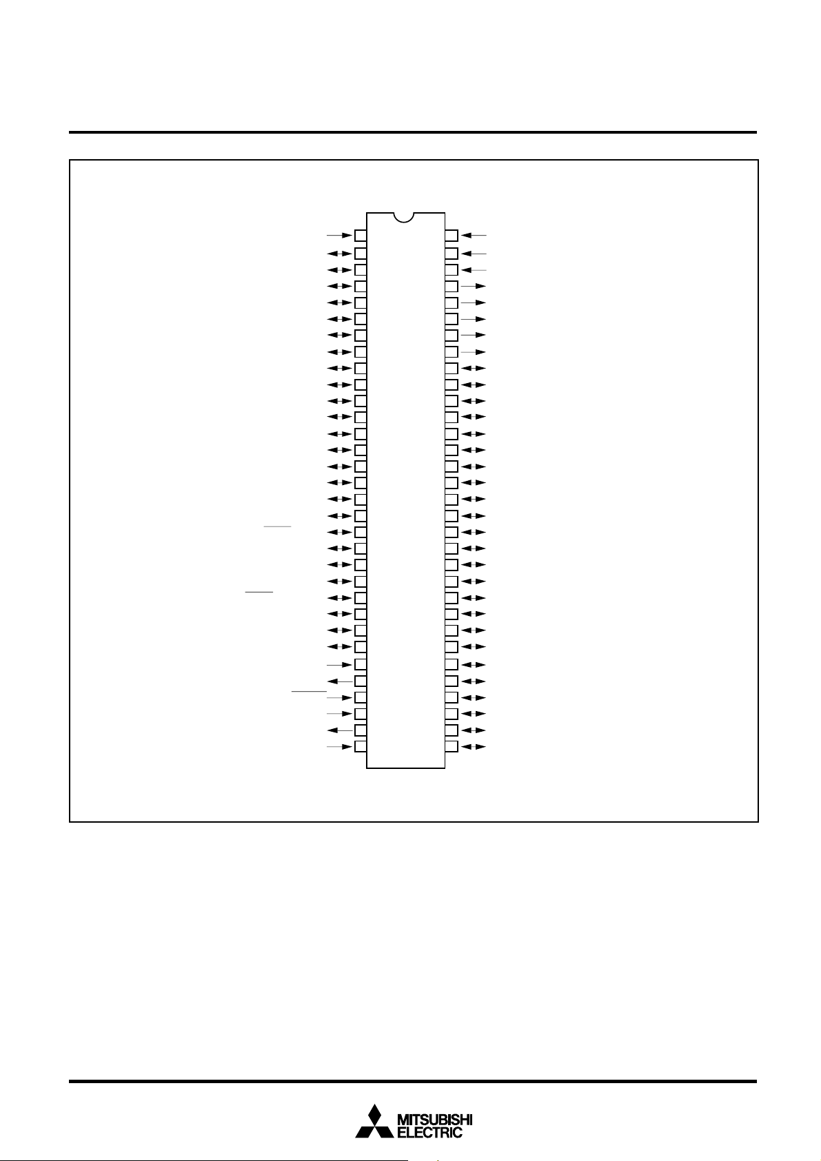
PIN CONFIGURATION (TOP VIEW)
MITSUBISHI MICROCOMPUTERS
M37207MF-XXXSP/FP, M37207M8-XXXSP
M37207EFSP/FP
SINGLE-CHIP 8-BIT CMOS MICROCOMPUTER for VOLTAGE SYNTHESIZER
and ON-SCREEN DISPLAY CONTROLLER
P4
P4
P4
3
P4
1/SCLK2
0/SOUT2
OSC1/P70/AD4
OSC2/P7
P3
6
/INT2/AD2
P3
P3
4
D-A/AD3
0
/PWM0
P6
1
/PWM1
P6
P62/PWM2
P6
3
/PWM3
4
/PWM4
P6
P65/PWM5
6
/PWM6
P6
7
/PWM7
P6
P3
3
2
/TIM2/AD6
P3
P47/
S
RDY1
/PWM8
6/SIN1
5/SCLK1
4/SOUT1
RDY2
/SCL2/AD7
/SDA2/AD8
/PWM9
/SCL1
/SDA1
P4
P4
P4
/
S
2/SIN2
/SCL3/X
/SDA3/X
CNV
RESET
1
/AD5
5
/AD1
/INT1
/TIM3
P3
P3
COUT
CIN
X
X
OUT
V
SS
SS
1
2
3
4
5
6
7
8
9
M37207EFSP
10
11
12
13
14
15
16
17
1
18
0
19
20
21
22
23
24
25
26
27
28
φ
29
30
IN
31
32
64
V
CC
63
H
SYNC
62
V
SYNC
61
R/P5
2
60
G/P5
3
59
B/P5
4
58
I/P55/TIM1 OVERFLOW
57
OUT/P5
6
56
P0
M37207MF-XXXSP, M37207M8-XXXSP
55
54
53
52
51
50
49
48
47
46
45
44
43
42
41
40
39
38
37
36
35
34
33
P0
P0
P0
P0
P0
P0
P0
P1
P1
P1
P1
P1
P1
P1
P1
P2
P2
P2
P2
P2
P2
P2
P2
0
1
2
3
4
5
6
7
0
1
2
3
4
5
6
7
0
1
2
3
4
5
6
7
Outline 64P4B
2
Page 3
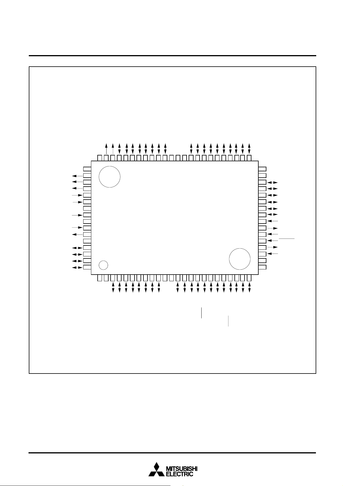
PIN CONFIGURATION (TOP VIEW)
6
/TIM1 OVERFLOW
5
0
1
P0
I/P5
OUT/P5
NC
B/P5
G/P5
R/P5
V
SYNC
H
SYNC
NC
V
NC
OSC1/P70/AD4
OSC2/P7
1
/AD5
NC
6
/INT2/AD2
P3
5
/AD1
P3
P3
4
/INT1
D-A/AD3
CC
NC
63
64
65
4
66
67
3
68
2
69
70
71
72
73
74
75
76
77
78
79
80
2
1
P0
62
60
61
4
5
3
MITSUBISHI MICROCOMPUTERS
M37207MF-XXXSP/FP, M37207M8-XXXSP
M37207EFSP/FP
SINGLE-CHIP 8-BIT CMOS MICROCOMPUTER for VOLTAGE SYNTHESIZER
and ON-SCREEN DISPLAY CONTROLLER
4
P0
57
8
56
9
5
P0
6
7
NC
P0
P0
55
53
54
12
10
11
NC
52
13
NC
51
14
0
1
P1
P1
50
49
151617
2
P1
48
3
P1
47
18
4
P1
46
19
5
P1
45
20
6
P1
44
21
7
P1
43
22
42
23
0
P2
41
24
1
P2
40
39
38
37
36
35
34
33
32
31
30
29
28
27
26
25
NC
NC
P2
2
P2
3
P2
4
P2
5
P2
6
P2
7
V
SS
OUT
X
X
IN
RESET
φ
CNV
SS
NC
NC
3
2
P0
P0
59
58
M37207MF-XXXFP, M37207EFFP
7
6
NC
NC
/PWM0
/PWM1
0
1
P6
P6
/PWM2
/PWM3
2
3
P6
P6
NC
NC
/PWM6
/PWM4
4
P6
/PWM5
6
5
P6
P6
/PWM7
7
P6
Outline 80P6N-A
/TIM3
3
P3
/TIM2/AD6
2
P3
1
P3
0
P3
/PWM9
IN1
/S
6
/SRDY1/PWM8
7
P4
P4
/SCL1
/SDA1
CLK1
OUT1
/S
/S
5
4
P4
P4
COUT
/SDA2/AD8
/SCL3/X
IN2
/S
/SRDY2/SCL2/AD7
2
CLK2
3
/S
P4
1
P4
P4
CIN
/SDA3/X
OUT2
P4φ/S
NC: Unconnected
3
Page 4
M37207MF-XXXSP/FP, M37207M8-XXXSP
SINGLE-CHIP 8-BIT CMOS MICROCOMPUTER for VOLTAGE SYNTHESIZER
1
, P7
0
Input ports P7
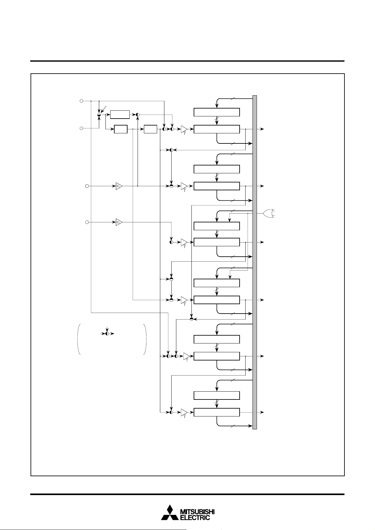
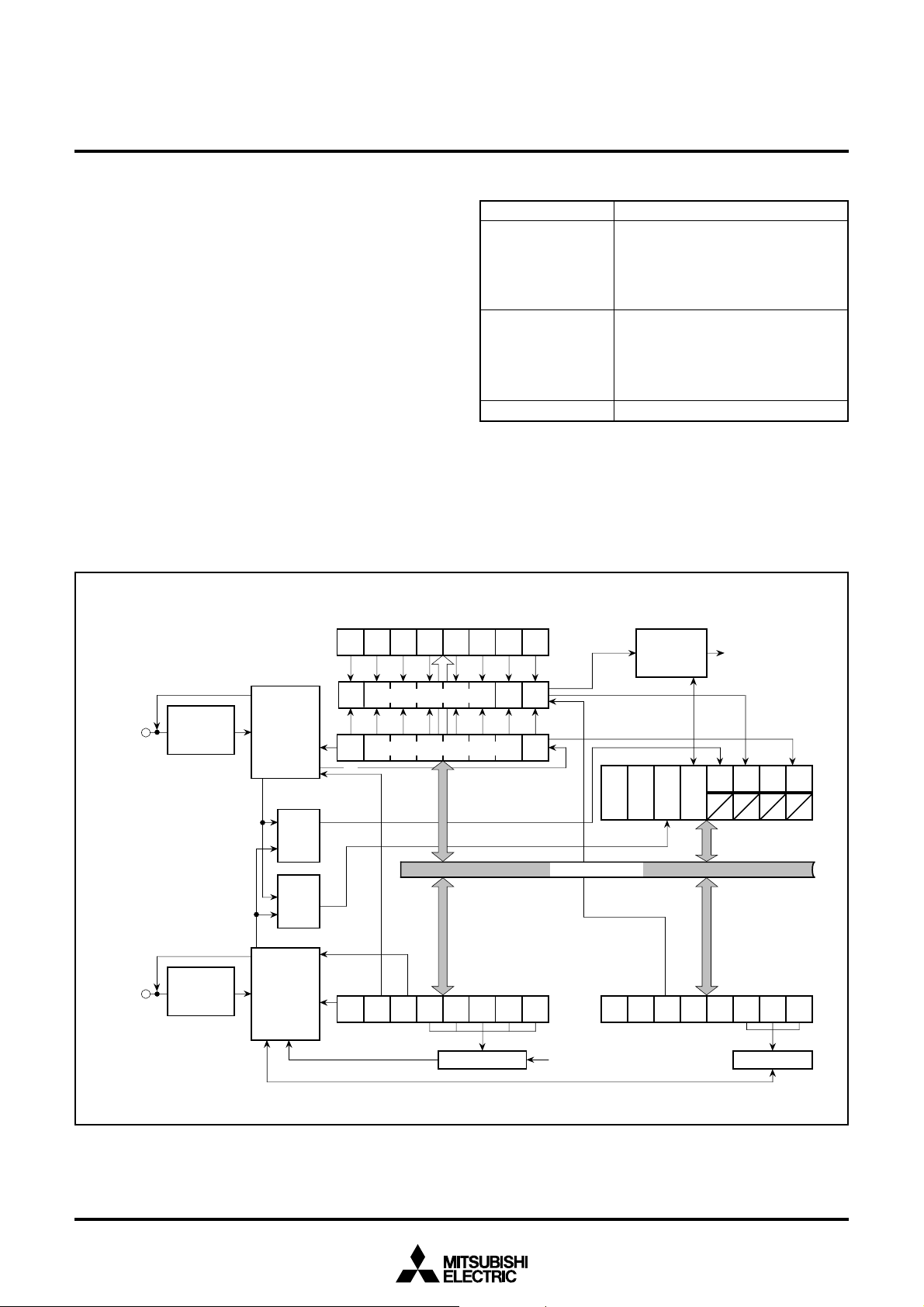
FUNCTIONAL BLOCK DIAGRAM of M37207M8-XXXSP
2
OSC2
Clock output for CRT/
Sub-clock output
1
OSC1
Sub-clock input
Clock input for CRT/
SS
27
CNV
SS
32
V
CC
64
V
29
RESET
Reset input
Timing output
φ
28
OUT
31
X
Clock
output
IN
30
X
input
Clock
A-D comparator
Timer count source
TIM2
Data bus
Clock
circuit
generating
selection circuit
T1 (8)
Timer 1
TIM3
ROM
64 K bytes
(Note 2)
counter
Program
counter
Program
RAM
960 bytes
(Note 1)
COUT
X
CIN
X
(8)
L
PC
(8)
H
PC
T2 (8)
Timer 2
Address bus
T3 (8)
Timer 3
Instruction
Control signal
T4 (8)
Timer 4
Stack
pointer
Index
register
Index
register
status
processor
A (8)
Accumulator
8-bit
arithmetic
decoder
Timer 5
S (8)
Y (8)
X (8)
register
and
CRT circuit
instruction
T5 (8)
PS (8)
logical unit
MITSUBISHI MICROCOMPUTERS
M37207EFSP/FP
and ON-SCREEN DISPLAY CONTROLLER
H
SYNC
63
V
SYNC
62
input
Sync
61
60
59
58
57
Output ports
7
87
–P6
0
9
10
11
12
I/O ports P6
13
14
19
20
7
21
–P4
0
22
24 23
25
26
I/O ports P4
6
D-A
18
17
16
15
5
I/O ports
34
40
39
38
37
I/O ports
35 36
34
33
48
47
46
45
44
I/O ports
43
42
41
56
55
54
53
52
I/O ports
51
50
49
6
–P5
2
P5
6
–P3
0
P3
7
–P2
0
P2
7
–P1
0
P1
7
–P0
0
P0
register (8)
T6 (8)
Timer 6
PWM0
P5 (5)
PWM1
PWM2
PWM3
PWM4
PWM5
PWM6
PWM7
8-bit PWM circuit
P6 (8)
SCL1
SDA1
SCL2
SDA2
SCL3
SDA3
C-BUS Interface
2
Multi-master
I
S
RDY1
P4 (8)
S
IN1
S
CLK1
S
OUT1
S
RDY2
SI/O (8)
S
IN2
S
CLK2
S
OUT2
P3 (7)
INT2
INT1
P2 (8)
A-D
comparator
P1 (8)
P0(8)
14-bit
PWM circuit
R
G
B
I
OUT
Note 1: M37207M8-XXXSP has a 512 bytes RAM.
Note 2: M37207M8-XXXSP has a 32 K bytes ROM.
4
Page 5
FUNCTIONS
Parameter
Number of basic instructions
Instruction execution time
Clock frequency
Memory size
Input/Output ports
Serial I/O
Multi-master I2C-BUS interface
A-D comparator
PWM output circuit
Timers
ROM correction function
Subroutine nesting
Interrupt interval determination circuit
Interrupt
Clock generating circuit
M37207MF-XXXSP/FP, M37207M8-XXXSP
SINGLE-CHIP 8-BIT CMOS MICROCOMPUTER for VOLTAGE SYNTHESIZER
ROM
RAM
ROM correction memory
CRT ROM
CRT RAM
P00–P07
P10–P17
P20–P27
P30, P31
P32–P36
P40–P47
P52–P56
P60–P67
P70, P70
M37207M8-XXXSP
M37207MF-XXXSP/FP
M37207EFSP/FP
M37207M8-XXXSP
M37207MF-XXXSP/FP
M37207EFSP/FP
M37207M8-XXXSP
M37207MF-XXXSP/FP
M37207EFSP/FP
I/O
I/O
I/O
I/O
I/O
I/O
Output
I/O
Input
MITSUBISHI MICROCOMPUTERS
M37207EFSP/FP
and ON-SCREEN DISPLAY CONTROLLER
Functions
71
0.5 ms (the minimum instruction execution time, at 8 MHz oscillation frequency)
8 MHz (maximum)
32 K bytes
,
64 K bytes
512 bytes
960 bytes
,
64 bytes
8K bytes
,
12K bytes
144 bytes
8-bit ✕ 1 (CMOS input/output structure)
8-bit ✕ 1 (CMOS input/output structure)
8-bit ✕ 1 (CMOS input/output structure)
2-bit ✕ 1 (CMOS input/output structure)
5-bit ✕ 1 (N-channel open-drain output structure, can be used as external
clock input pins, A-D input pins, INT input pins)
8-bit ✕ 1 (N-channel open-drain output structure, can be used as serial I/O
pins, A-D input pins, PWM output pins, multi-master I2C-BUS interface,
sub-clock I/O pins)
5-bit ✕ 1 (CMOS output structure, can be used as CRT output pins, an
external clock output pin)
8-bit ✕ 1 (N-channel open-drain output structure, can be used as PWM
output)
2-bit ✕ 1 (can be used as CRT display clock I/O pins, analog input pins)
8-bit ✕ 1 (2 systems)
1 (3 systems)
8 channels (6-bit resolution)
14-bit ✕ 1, 8-bit ✕ 10
8-bit timer ✕ 6
32 bytes ✕ 2
128 levels (maximum)
1
External interrupt ✕ 2, Internal timer interrupt ✕ 6, Serial I/O interrupt ✕ 1,
CRT interrupt ✕ 1, Multi-master I2C-BUS interface interrupt ✕ 1,
f(XIN)/4096 interrupt ✕ 1, VSYNC interrupt ✕ 1, BRK interrupt ✕ 1
2 built-in circuits (externally connected to a ceramic resonator or a quartzcrystal oscillator)
5
Page 6
FUNCTIONS (continued)
Parameter
Power source voltage
Power dissipation
Operating temperature range
Device structure
Package
CRT display
function
In high-speed
mode
In low-speed
mode
In stop mode
M37207MF-XXXSP, M37207M8-XXXSP
M37207EFSP
M37207MF-XXXFP, M37207EFFP
Number of display characters
Character display area
Kinds of
characters
Kinds of character sizes
Kinds of character colors
Display position (horizontal, vertical)
M37207MF-XXXSP/FP, M37207M8-XXXSP
SINGLE-CHIP 8-BIT CMOS MICROCOMPUTER for VOLTAGE SYNTHESIZER
CRT ON
CRT OFF
CRT OFF
M37207M8-XXXSP
M37207MF-XXXSP/FP,
M37207EFSP/FP
MITSUBISHI MICROCOMPUTERS
M37207EFSP/FP
and ON-SCREEN DISPLAY CONTROLLER
Functions
5 V ± 10 %
165 mW typ. (at oscillation frequency f(XIN) = 8 MHz, fOSC = 8 MHz)
82.5 mW typ. (at oscillation frequency f(XIN) = 8 MHz)
0.33 mW typ. (at oscillation frequency fCLK = 32 kHz, f(XIN) = stopped)
1.1 mW (maximum)
–10 °C to 70 °C
CMOS silicon gate process
64-pin shrink plastic molded DIP
80-pin plastic molded QFP
24 characters ✕ 3 lines (maximum 16 lines by software)
12 ✕ 16 dots
256 Kinds
384 Kinds
4 kinds
Maximum 15 kinds (R, G, B, I); can be specified by the character
64 levels (horizontal) ✕ 128 levels (vertical)
6
Page 7
M37207MF-XXXSP/FP, M37207M8-XXXSP
SINGLE-CHIP 8-BIT CMOS MICROCOMPUTER for VOLTAGE SYNTHESIZER
PIN DESCRIPTION
Pin Functions
VCC, VSS
Name
Power source
Input/
Output
Apply voltage of 5 V ± 10 % (typical) to VCC and AVCC, and 0 V to VSS.
MITSUBISHI MICROCOMPUTERS
M37207EFSP/FP
and ON-SCREEN DISPLAY CONTROLLER
CNVSS
______
RESET
XIN
XOUT
P00–P07
P10–P17
P20–P27
P30, P31
P32/TIM2/
AD6,
P33/TIM3,
P34/INT1,
P35/AD1,
P36/INT2/
AD2
P40/SOUT2/
SDA3/XCIN,
P41/SCLK2/
SCL3/
XCOUT, P42/
SIN2/SDA2/
AD8,
_____
P43/SRDY2/
SCL2/AD7,
P44/SOUT1/
SDA1,
P45/SCLK1/
SCL1,
P46/SIN1/
PWM9,
_____
P47/SRDY1/
PWM8
CNVSS
Reset input
Clock input
Clock output
I/O port P0
I/O port P1
I/O port P2
I/O port P3
I/O port P3
Analog input
External clock
input
External interrupt
input
I/O port P4
Serial I/O data
input/output
Serial I/O synchronous clock input/
output
Serial I/O receive
enable signal output
Multi-master I2CBUS interface
Sub-clock input
Sub-clock output
Analog input
PWM output
Input
Input
Output
I/O
I/O
I/O
I/O
I/O
Input
Input
Input
I/O
I/O
I/O
Output
I/O
Input
Output
Input
Output
Connected to VSS.
To enter the reset state, the reset input pin must be kept at a “L” for 2 ms or more (under
normal VCC conditions).
If more time is needed for the quartz-crystal oscillator to stabilize, this “L” condition should
be maintained for the required time.
This chip has an internal clock generating circuit. To control generating frequency, an
external ceramic resonator or a quartz-crystal oscillator is connected between pins XIN and
XOUT. If an external clock is used, the clock source should be connected to the XIN pin and
the XOUT pin should be left open.
Port P0 is an 8-bit I/O port with direction register allowing each I/O bit to be individually
programmed as input or output. At reset, this port is set to input mode. The output structure
is CMOS output. See notes at end of table for full details of port P0 functions.
Port P1 is an 8-bit I/O port and has basically the same functions as port P0. The output
structure is CMOS output.
Port P2 is an 8-bit I/O port and has basically the same functions as port P0. The output
structure is CMOS output.
Ports P30, P31 are 2-bit I/O ports and have basically the same functions as port P0. The
output structure is CMOS output.
Ports P32–P36 are 5-bit I/O ports and have basically the same functions as port P0. The
output structure is N-channel open-drain output.
Pins P32, P35, P36 are also used as analog input pins AD6, AD1 and AD2 respectively.
Pins P32, P33 are also used as external clock input pins TIM2, TIM3 respectively.
Pins P34, P36 are also used as external interrupt input pins INT1, INT2.
Port P4 is an 8-bit I/O port and has basically the same functions as port P0. The output
structure is N-channel open-drain output.
Pins P40, P42, P44, P46 are also used as serial I/O data input/output pins SOUT2, SIN2,
SOUT1, SIN1 respectively. The output structure is N-channel open-drain output.
Pins P41, P45 are also used as serial I/O synchronous clock input/output pins SCLK2, SCLK1
respectively.
Pins P43, P47 are also used as serial I/O receive enable signal output pins SRDY2, SRDY1
respectively. The output structure is N-channel open-drain output.
Pins P40–P45 are also used as SDA3, SCL3, SDA2, SCL2, SDA1, SCL1 respectively
when multi-master I2C-BUS interface is used. The output structure is N-channel opendrain output.
Pin P40 is also used as sub-clock input pin XCIN.
Pin P41 is also used as sub-clock output pin XCOUT. The output structure is N-channel
open-drain output.
Pins P42, P43 are also used as analog input pins AD8, AD7 respectively.
Pins P46, P47 are also used as PWM output pins PWM9, PWM8 respectively. The output
structure is N-channel open-drain output.
_____ _____
7
Page 8
PIN DESCRIPTION (continued)
MITSUBISHI MICROCOMPUTERS
M37207MF-XXXSP/FP, M37207M8-XXXSP
M37207EFSP/FP
SINGLE-CHIP 8-BIT CMOS MICROCOMPUTER for VOLTAGE SYNTHESIZER
and ON-SCREEN DISPLAY CONTROLLER
Pin Name
R/P52,
G/P53,
B/P54,
I/P55/TIM1
OVERFLOW,
OUT/P56
P60/PWM–
P67/PWM7
OSC1/P70/
AD4,
OSC2/P71/
AD5
HSYNC
VSYNC
f
D-A/AD3
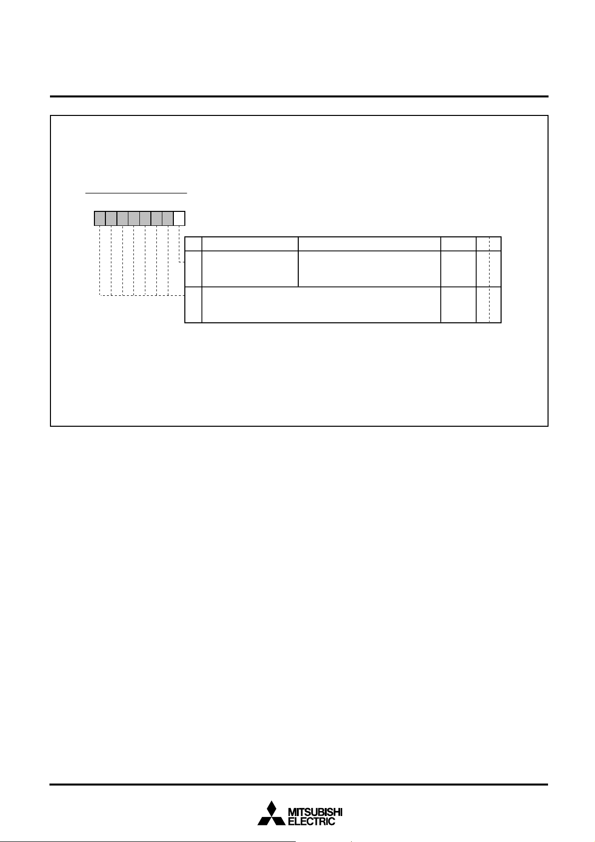
Note : As shown in the memory map (Figure 5), port P0 is accessed as a memory at address 00C016 of zero page. Port P0 has the port P0
direction register (address 00C116 of zero page) which can be used to program each bit as an input (“0”) or an output (“1”). The pins
programmed as “1” in the direction register are output pins. When pins are programmed as “0,” they are input pins. When pins are
programmed as output pins, the output data are written into the port latch and then output. When data is read from the output pins, the
output pin level is not read but the data of the port latch is read. This allows a previously-output value to be read correctly even if the
output “L” voltage has risen, for example, because a light emitting diode was directly driven. The input pins float, so the values of the pins
can be read. When data is written into the input pin, it is written only into the port latch, while the pin remains in the floating state.
Output port
P5
CRT output
Timer 1 overflow
signal output
I/O port P6
PWM output
Input port P7
Clock input
for CRT
display
Clock output
for CRT
display
Analog input
HSYNC input
VSYNC input
Timing
output
DA output
Analog input
Input/
Output
Output
Output
Output
I/O
Output
Input
Input
Output
Input
Input
Input
Output
Output
Input
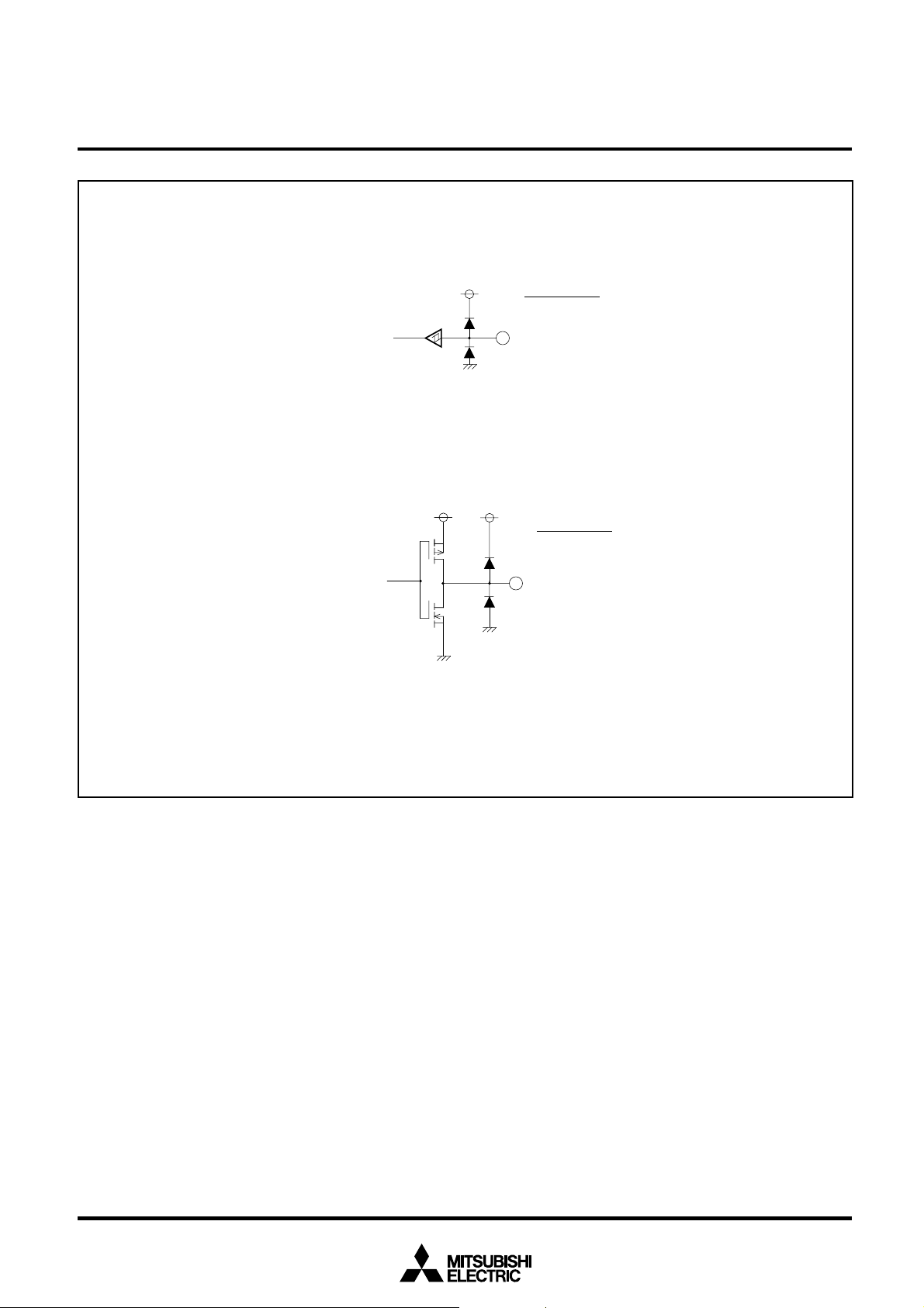
Ports P52–P56 are 5-bit output ports. The output structure is CMOS output.
Pins P52–P56 are also used as CRT output pins R, G, B, I, OUT respectively. The output structure
is CMOS output.
Pin P55 is also used as timer 1 overflow signal output pin TIM1 OVERFLOW. The output structure is
CMOS output.
Port P6 is an 8-bit I/O port and has basically the same functions as port P0. The output structure is
N-channel open-drain output.
Pins P60–P67 are also used as PWM output pins PWM0–PWM7. The output structure is CMOS
output.
Ports P70, P71 are 2-bit input port.
Pin P70 is also used as CRT display clock input pin OSC1.
Pin P71 is also used as CRT display clock output pin OSC2. The output structure is CMOS output.
Pins P70, P71 are also used as analog input pins AD4, AD5 respectively.
This is a horizontal synchronous signal input for CRT display.
This is a vertical synchronous signal input for CRT display.
This is a timing output pin. This pin has reset-out output function. The output structure is CMOS
output.
This is an output pin for 14-bit PWM.
The D-A pin is also used as analog input pin AD3.
Functions
8
Page 9
SINGLE-CHIP 8-BIT CMOS MICROCOMPUTER for VOLTAGE SYNTHESIZER
Ports P00–P07, P10–P17, P20–P27, P30, P31, D-A
Direction register
MITSUBISHI MICROCOMPUTERS
M37207MF-XXXSP/FP, M37207M8-XXXSP
M37207EFSP/FP
and ON-SCREEN DISPLAY CONTROLLER
CMOS output
Data bus
Ports P4
6, P47, P60–P67
Data bus
Ports P32–P36, P42–P45
Port latch
Direction register
Port latch
Direction register
Ports P00–P07, P10–P17,
P20–P27, P30, P31, D-A
Note : D-A pin is also used as
AD3.
N-channel open-drain output
Ports P46, P47, P60–P67
Note : Each port is also used as
follows:
P46 : SIN1/PWM9
_____
P47 : SRDY1/PWM8
P60–P67 : PWM0–PWM7
N-channel open-drain output
Data bus
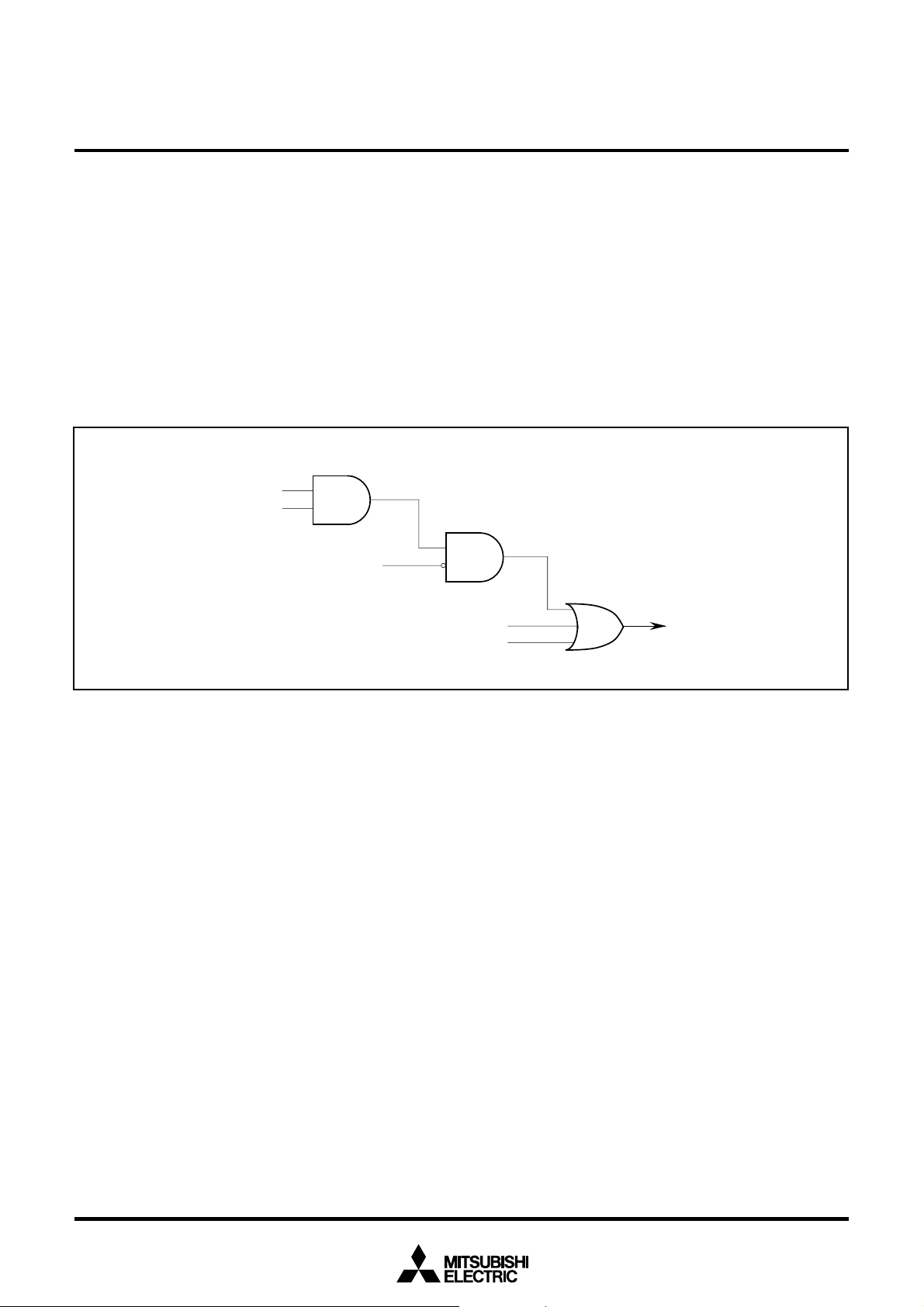
Fig. 1. I/O Pin Block Diagram (1)
Port latch
Ports P32–P36, P42–P45
Note : Each port is also used as
follows:
P32 : TIM2/AD6
P33 : TIM3
P34 : INT1
P35 : AD1
P36 : INT2/AD2
P42 : SIN2/SDA2/AD8
_____
P43 : SRDY2/SCL2/AD7
P44 : SOUT1/SDA1
P45 : SCLK1/SCL1
9
Page 10
SYNC, VSYNC
H
MITSUBISHI MICROCOMPUTERS
M37207MF-XXXSP/FP, M37207M8-XXXSP
M37207EFSP/FP
SINGLE-CHIP 8-BIT CMOS MICROCOMPUTER for VOLTAGE SYNTHESIZER
and ON-SCREEN DISPLAY CONTROLLER
Schmidt input
Internal circuit
R, G, B, I, OUT,
P52–P55, φ
Internal circuit
HSYNC, VSYNC
CMOS output
P52–P55, φ
Note : Each port is also used as follows:
P52 : R
P53 : G
P54 : B
P55 : I/TIM1
P56 : OUT
Fig. 2. I/O Pin Block Diagram (2)
10
Page 11
MITSUBISHI MICROCOMPUTERS
M37207MF-XXXSP/FP, M37207M8-XXXSP
M37207EFSP/FP
SINGLE-CHIP 8-BIT CMOS MICROCOMPUTER for VOLTAGE SYNTHESIZER
and ON-SCREEN DISPLAY CONTROLLER
FUNCTIONAL DESCRIPTION
Central Processing Unit (CPU)
This microcomputer uses the standard 740 Family instruction set.
Refer to the table of 740 Family addressing modes and machine
instructions or the SERIES 740 <Software> User’s Manual for details on the instruction set.
Machine-resident 740 Family instructions are as follows:
The FST, SLW instruction cannot be used.
The MUL, DIV, WIT and STP instructions can be used.
CPU Mode Register
b7b6 b5b4b3 b2b1b0
1
00
CPU mode register (CPUM) (CM) [Address 00FB16]
B
0, 1
Name Functions
Processor mode bits
(CM0, CM1)
Stack page selection
2
bit (CM2) (See note 1)
CPU Mode Register
The CPU mode register contains the stack page selection bit and
internal system clock selection bit. The CPU mode register is allocated at address 00FB16.
After reset
b1 b0
0 0: Single-chip mode
0 1:
1 0: Not available
1 1:
0: 0 page
1: 1 page
RW
RW
0
RW
1
Fig. 3. CPU Mode Register
3
Fix these bits to “1.”
Internal system clock
41
output selection bit
(CM4) (See note 2)
X
COUT
51
drivability
selection bit (CM5)
Main Clock (X
60
IN–XOUT
stop bit
(CM6)
Internal system clock
70
selection bit
(CM7)
0: Output is stopped
1: Internal system
clock
φ
output
0: LOW drive
1: HIGH drive
)
0: Oscillating
1: Stopped
0: X
IN–XOUT
selected
(high-speed mode)
1: X
CIN–XCOUT
selected
RW
1
RW
RW
RW
RW
(high-speed mode)
Notes 1: This bit is set to “1” after the reset release.
φ
2: The internal system clock
stops at HIGH.
11
Page 12
MITSUBISHI MICROCOMPUTERS
M37207MF-XXXSP/FP, M37207M8-XXXSP
M37207EFSP/FP
SINGLE-CHIP 8-BIT CMOS MICROCOMPUTER for VOLTAGE SYNTHESIZER
and ON-SCREEN DISPLAY CONTROLLER
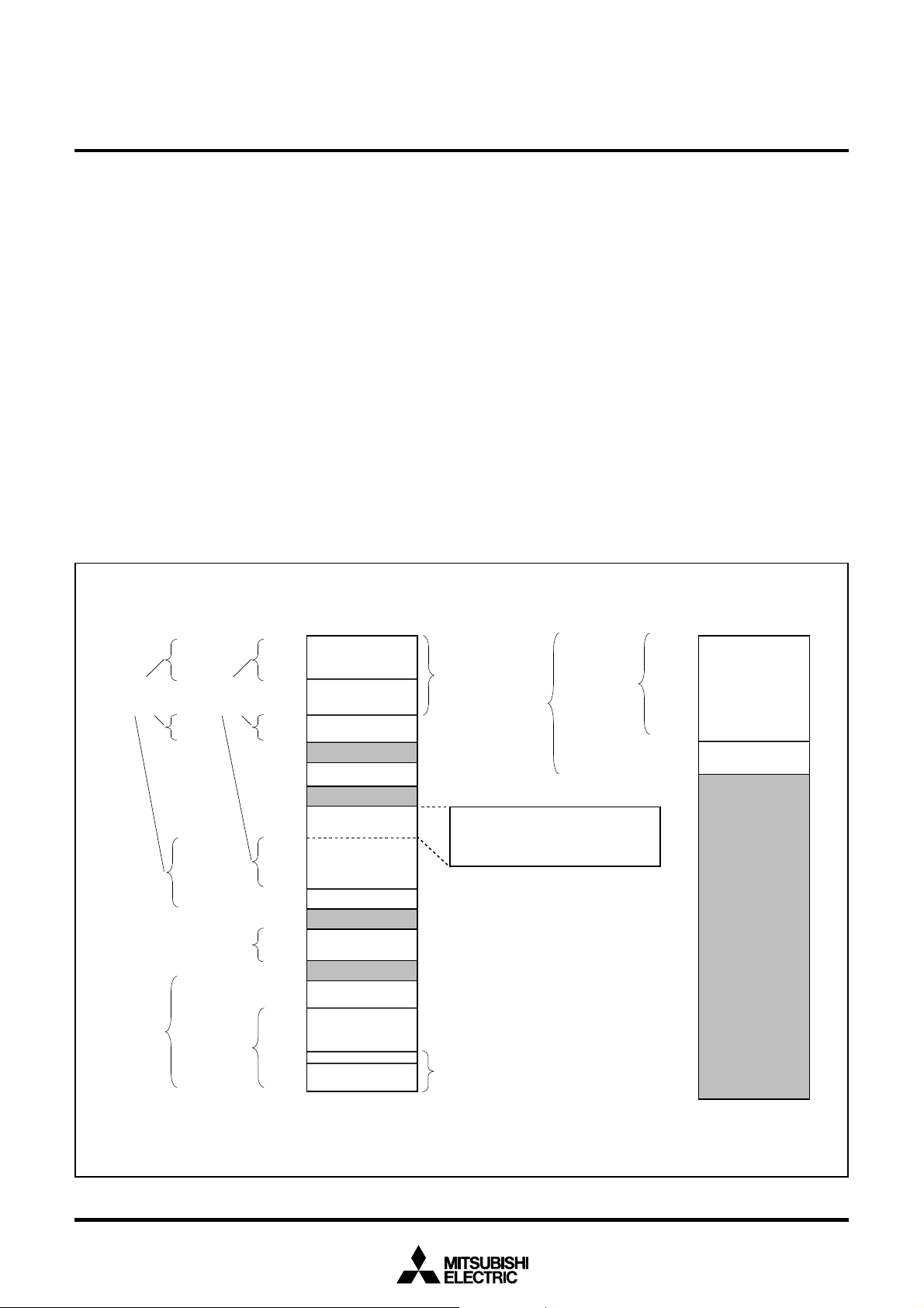
MEMORY
Special Function Register (SFR) Area
The special function register (SFR) area in the zero page contains
control registers such as I/O ports and timers.
RAM
RAM is used for data storage and for stack area of subroutine calls
and interrupts.
ROM
ROM is used for storing user programs as well as the interrupt vector
area.
RAM for Display
RAM for display is used for specifying the character codes and colors to display.
ROM for Display
ROM for display is used for storing character data.
000016
Interrupt Vector Area
The interrupt vector area contains reset and interrupt vectors.
Zero Page
The 256 bytes from addresses 000016 to 00FF16 are called the zero
page area. The internal RAM and the special function registers (SFR)
are allocated to this area.
The zero page addressing mode can be used to specify memory and
register addresses in the zero page area. Access to this area with
only 2 bytes is possible in the zero page addressing mode.
Special Page
The 256 bytes from addresses FF0016 to FFFF16 are called the special page area. The special page addressing mode can be used to
specify memory addresses in the special page area. Access to this
area with only 2 bytes is possible in the special page addressing
mode.
ROM Correction Memory (RAM)
This is used as the program area for ROM correction.
10000
16
RAM
(960 bytes)
for M37207MF
ROM
(62 K bytes)
for M37207MF
RAM
(512 bytes)
for M37207M8
RAM
for display
(144 bytes)
(See note)
ROM
(32 K bytes)
for M37207M8
00C016
00FF16
01FF16
020416
021B16
02C016
02FF16
030016
033F16
04FF16
060016
06D716
080016
800016
FF0016
FFDE16
FFFF
SFR area
Not used
2 page register
Not used
Not used
Not used
Interrupt vector area
16
Zero page
ROM
for display
(12 K bytes)
for M37207MF
ROM correction memory (64 bytes)
Block 1: addresses 02C0
Block 2: addresses 02E016 to 02FF16
Special page
for display
(8 K bytes)
for M37207M8
Note: Refer to Table 9. Contents of CRT display RAM.
ROM
11FFF16
12FFF16
16 to 02DF16
Not used
1FFFF16
Fig. 4. Memory Map
12
Page 13
M37207MF-XXXSP/FP, M37207M8-XXXSP
SINGLE-CHIP 8-BIT CMOS MICROCOMPUTER for VOLTAGE SYNTHESIZER
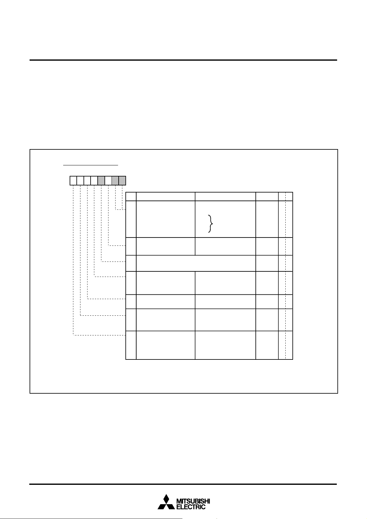
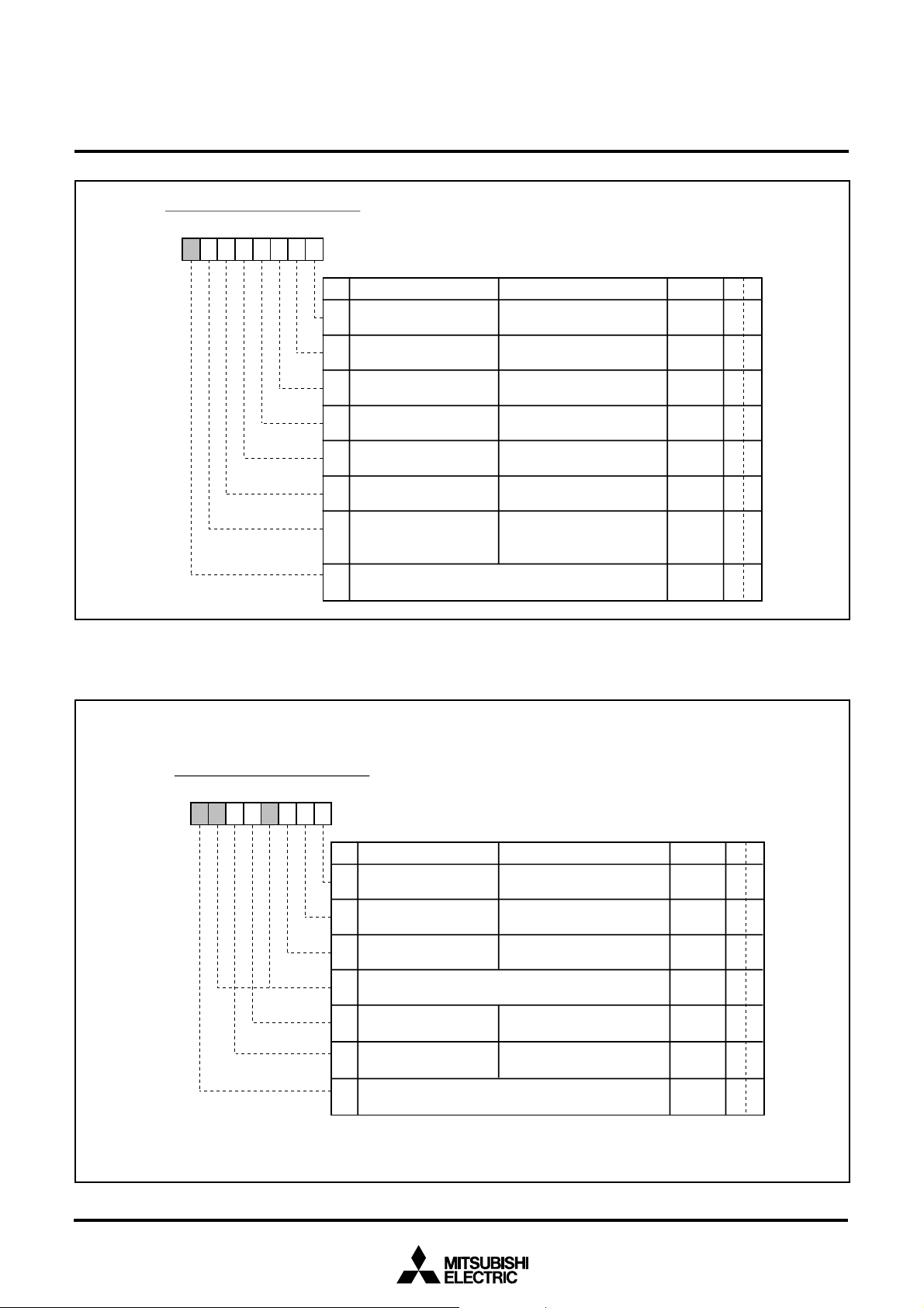
■SFR Area (addresses C016 to DF16)
<Bit allocation>
:
Name
:
: No function bit
: Fix this bit to “0”
0
(do not write “1”)
: Fix this bit to “1”
1
(do not write “0”)
Function bit
MITSUBISHI MICROCOMPUTERS
M37207EFSP/FP
and ON-SCREEN DISPLAY CONTROLLER
<State immediately after reset>
: “0” immediately after reset
0
1
: “1” immediately after reset
: Undefined immediately
?
after reset
Address
Port P0 (P0)
C0
16
Port P0 direction register (D0)
C1
16
Port P1 (P1)
C2
16
Port P1 direction register (D1)
C3
16
Port P2 (P2)
C4
16
Port P2 direction register (D2)
C5
16
Port P3 (P3)
C6
16
Port P3 direction register (D3)
C7
16
C8
16
Port P4 (P4)
Port P4 direction register (D4)
C9
16
Port P5 (P5)
CA
16
Port P5 control register (D5)
CB
16
CC
16
Port P6 (P6)
Port P6 direction register (D6)
CD
16
DA-H register (DA-H)
CE
16
DA-L register (DA-L)
CF
16
PWM0 register (PWM0)
D0
16
PWM1 register (PWM1)
D1
16
PWM2 register (PWM2)
D2
16
PWM3 register (PWM3)
D3
16
PWM4 register (PWM4)
D4
16
PWM output control register 1 (PW)
D5
16
PWM output control register 2 (PN)
D6
16
Interrupt interval determination register (??)
D7
16
Interrupt interval determination control register (RE)
D8
16
D9
DA
DB
DC
DD
DE
DF
2
16
C data shift register (S0)
I
16
I2C address register (S0D)
16
I2C status register (S1)
16
I2C control register (S1D)
16
I2C clock control register (S2)
16
Serial I/O mode register (SM)
16
Serial I/O regsiter (SIO)
Register
b7 b0
ACK
Bit allocation State immediately after reset
PW0PW1PW2PW3PW4PW5PW6PW7
PN2PN3PN4
PN1 PN0
RE1RE2RE3RE4RE5 RE0
D1D2D3D4D5D6D7 D0
SAD0SAD1SAD2SAD3SAD4SAD5SAD6
RBW
LRBAD0AASALPINBBTRXMST
BC0BC1BC2ESOALS
CCR0CCR1CCR2CCR3CCR4
SM0SM1SM2SM3SM5SM6
BSEL0BSEL1
ACK
BIT
10BIT
SAD
FAST
MODE
0
b7 b0
?
16
00
?
16
00
?
16
00
??0
00
16
?????
?
?
0
?
00
????
16
?
?
?
00
16
?
00
??????
?
?
?
?
?
16
00
16
00
?
00
16
?
00
16
00 0 010 0?
00
16
00
16
00
16
?
Fig. 5. Memory Map of Special Function Register (SFR)
13
Page 14
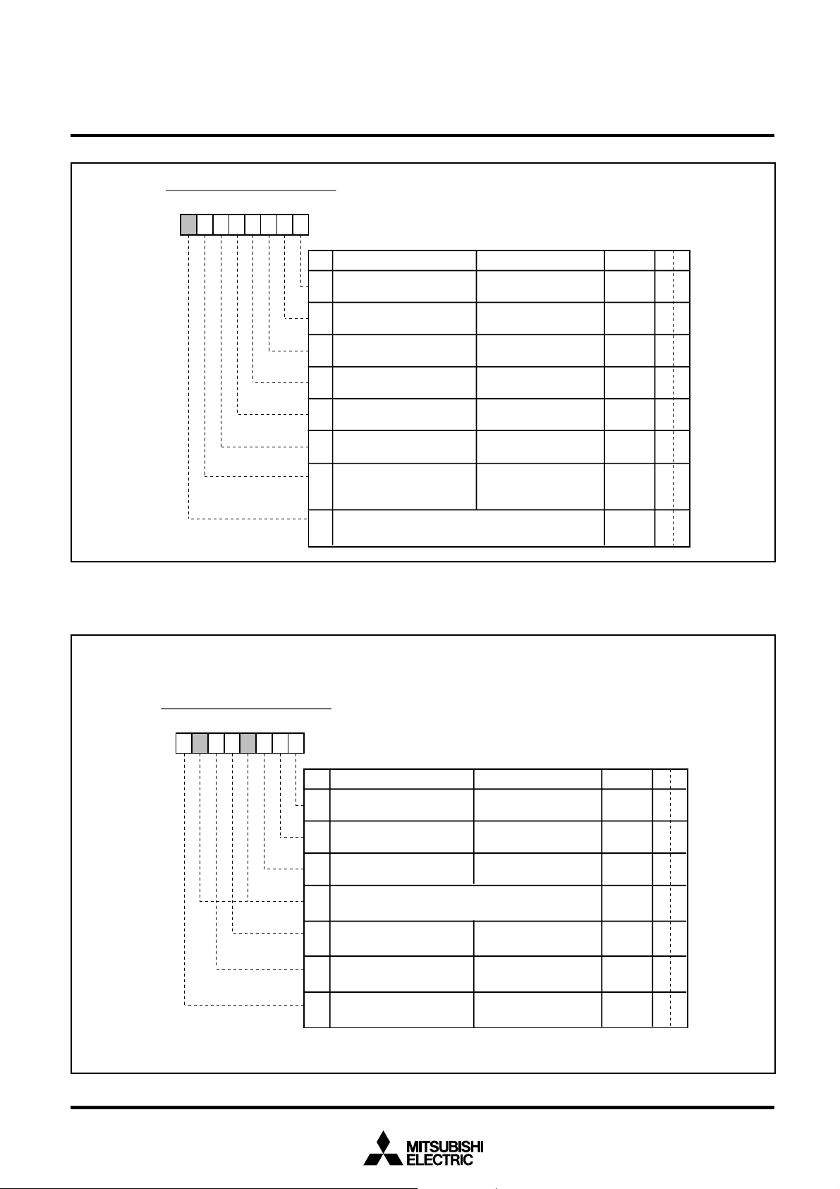
■
SFR Area (addresses E0
MITSUBISHI MICROCOMPUTERS
M37207MF-XXXSP/FP, M37207M8-XXXSP
M37207EFSP/FP
SINGLE-CHIP 8-BIT CMOS MICROCOMPUTER for VOLTAGE SYNTHESIZER
and ON-SCREEN DISPLAY CONTROLLER
16
to FF16)
Address
E0
16
E1
16
E2
16
E3
16
E4
16
E5
16
E6
16
E7
16
E8
16
E9
16
EA
16
EB
16
EC
16
ED
16
EE
16
EF
16
F0
16
F1
16
F2
16
F3
16
F4
16
F5
16
F6
16
F7
16
F8
16
F9
16
FA
16
FB
16
FC
16
FD
16
FE
16
FF
16
Register
Horizontal register (HR)
Vertical register 1 (CV1)
Vertical register 2 (CV2)
Vertical register 3 (CV3)
Character size register (CS)
Border selection register (MD)
Color register 0 (CO0)
Color register 1 (CO1)
Color register 2 (CO2)
Color register 3 (CO3)
CRT control register 1 (CC)
Display block counter (CBC)
CRT port control register (CRTP)
Wipe mode register (SL)
Wipe start register (??)
A-D control register 1 (ADM)
Timer 1 (TM1)
Timer 2 (TM2)
Timer 3 (TM3)
Timer 4 (TM4)
Timer mode register 1 (TMR1)
Timer mode register 2 (TMR2)
PWM5 register (PWM5)
PWM6 register (PWM6)
PWM7 register (PWM7)
PWM8 register (PWM8)
PWM9 register (PWM9)
CPU mode register (CPUM)
Interrupt request register 1 (IREQ1)
Interrupt request register 2 (IREQ2)
Interrupt control register 1 (ICON1)
Interrupt control register 2 (ICON2)
<Bit allocation>
:
Function bit
Name
:
: No function bit
: Fix this bit to “0”
0
(do not write “1”)
: Fix this bit to “1”
1
(do not write “0”)
b7 b0
0
CS7
CO07
CO17
CO27
CO37
0
CM7 CM6 CM5
0
Bit allocation State immediately after reset
HR0HR1HR2HR3HR4HR5
CV10CV11CV12CV13CV14CV15CV16
CV20CV21CV22CV23CV24CV25CV26
CV30CV31CV32CV33CV34CV35CV36
CS10CS11CS20CS21
MD11MD21MD31MD30
MD10MD20
CO00
CO01CO02CO03CO05
CO11
CO11CO12CO13CO15
CO22
CO21CO22CO23CO25
CO33
CO31CO32CO33CO35
CC0CC1CC2
VSYC
HSYC
SL0SL1
ADM0ADM1ADM2ADM4
TMR10TMR11TMR12TMR13TMR14
TMR20TMR21TMR22TMR23TMR24TMR25TMR26TMR27
00
TM1RTM2RTM3RTM4RCRTRVSCRIICR
IT1RIT2R
TM1ETM2ETM3ETM4ECRTEVSCEIICE
IT1EIT2E
CO06
CO16
CO26
CO36
TMR15TMR16TMR17
TM56R
TM56ETM56C
CS30CS31
CO04
CO14
CO24
CO34
CC3CC4CC5CC6
IRGB
11
CK0MSR
R/G/B
SL2SL3SL4SL5SL6
CM2
S1R
SIEMSE
00
<State immediately after reset >
: “0” immediately after reset
0
: “1” immediately after reset
1
: Undefined immediately
?
after reset
b7 b0
00
16
0
??????
?
?0??????
?0??????
00??
00??? ?
00 000 00
????
??
00
16
00
16
00
16
00
16
00
16
00
16
00
16
00
16
00
16
?
FF
16
07
16
FF
16
07
16
00
16
00
16
?
?
?
?
?
0111 0010
CK0
00
00
00
00
16
16
16
16
Fig. 6. Memory Map of Special Function Register (SFR)
14
Page 15
M37207MF-XXXSP/FP, M37207M8-XXXSP
SINGLE-CHIP 8-BIT CMOS MICROCOMPUTER for VOLTAGE SYNTHESIZER
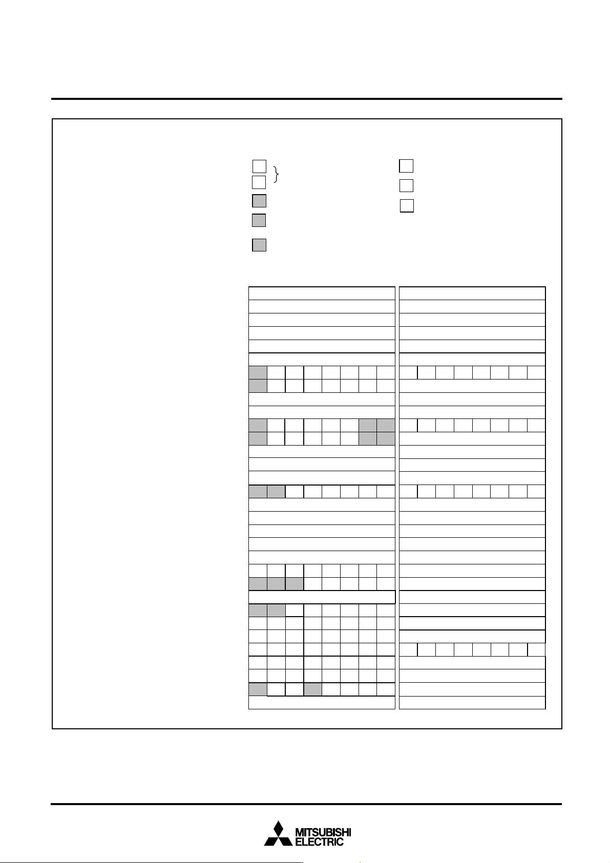
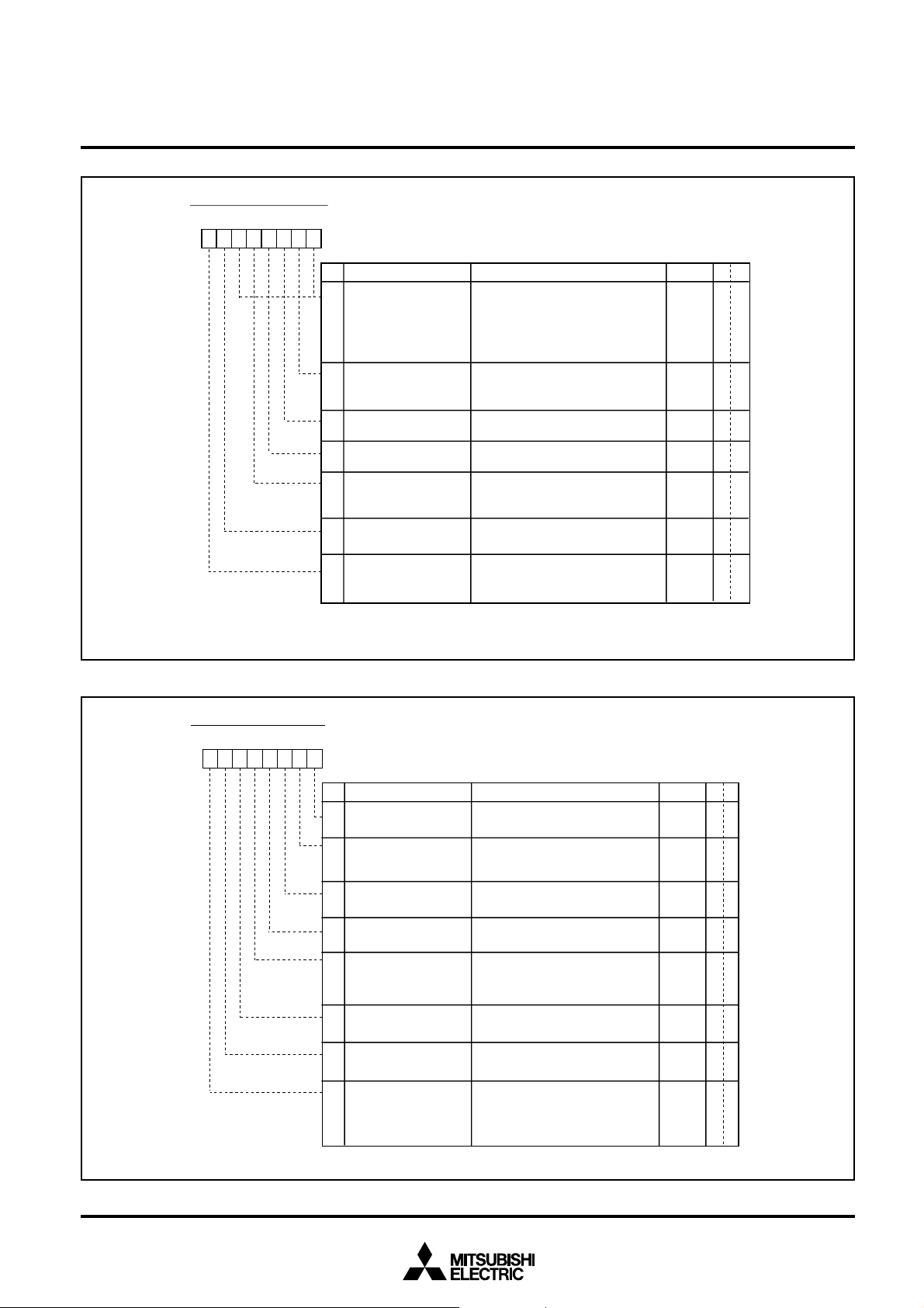
■SFR Area (addresses 20416 to 21B16)
MITSUBISHI MICROCOMPUTERS
M37207EFSP/FP
and ON-SCREEN DISPLAY CONTROLLER
Address
16
204
205
16
206
16
207
16
208
16
209
16
20A
16
20B
16
20C
16
20D
16
20E
16
20F
16
210
16
211
16
212
16
213
16
214
16
215
16
216
16
217
16
218
16
219
16
21A
16
21B
16
<Bit allocation>
Name
0
1
Register
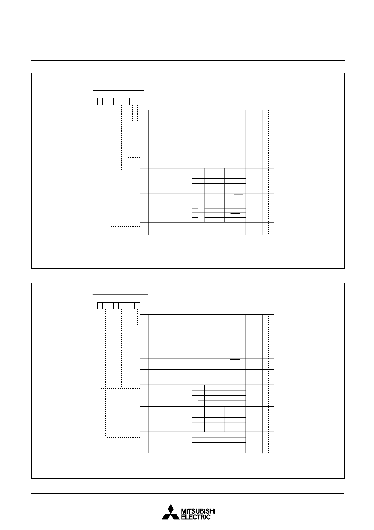
b7
Timer 5 (T5)
Timer 6 (T6)
Port control register (P7D)
Serial I/O control register (SIC)
CRT control register 2 (CBR)
CRT clock selection register (OP)
A-D control register (ADC)
Timer mode register (TMR3)
ROM correction address 1 (high-order)
ROM correction address 1 (low-order)
ROM correction address 2 (high-order)
ROM correction address 2 (low-order)
ROM correction enable register (RCR)
0
<State immediately after reset>
: “0” immediately after reset
b0
P7D0
SIC0SIC1SIC2SIC3SIC4SIC5SIC8SIC7
CBR0CBR1
ADC0ADC1ADC2ADC3ADC4ADC5
TMR30
0
: “1” immediately after reset
1
: Undefined immediately
?
after reset
b7
00
16
00
16
0000
00
16
00
16
00
16
00??
00
16
:
Function bit
:
: No function bit
: Fix this bit to “0”
(do not write “1”)
: Fix this bit to “1”
(do not write “0”)
Bit allocation State immediately after reset
P7D1P7D2P7D4
OP1OP0
?
?
?
?
?
?
?
?
?
?
?
00
16
00
16
00
16
00
16
0000
RC1RC0
????
00
??
b0
??
??
00
Fig. 7. Memory Map of 2 Page Register
15
Page 16
MITSUBISHI MICROCOMPUTERS
M37207MF-XXXSP/FP, M37207M8-XXXSP
M37207EFSP/FP
SINGLE-CHIP 8-BIT CMOS MICROCOMPUTER for VOLTAGE SYNTHESIZER
and ON-SCREEN DISPLAY CONTROLLER
<Bit allocation>
:
Function bit
Name
:
: No function bit
: Fix this bit to “0”
0
(do not write “1”)
: Fix this bit to “1”
1
(do not write “0”)
Register
b7
Processor status register (PS)
Program counter (PCH)
Program counter (PCL)
Fig. 8. Internal State of Processor Status Register and Program Counter at Reset
Bit allocation State immediately after reset
I ZCDBTVN???????
<State immediately after reset>
: “0” immediately after reset
0
1
: “1” immediately after reset
: Undefined immediately
?
after reset
b0
b7
Contents of address FFFF
Contents of address FFFE16
b0
1
16
16
Page 17
MITSUBISHI MICROCOMPUTERS
M37207MF-XXXSP/FP, M37207M8-XXXSP
M37207EFSP/FP
SINGLE-CHIP 8-BIT CMOS MICROCOMPUTER for VOLTAGE SYNTHESIZER
and ON-SCREEN DISPLAY CONTROLLER
INTERRUPTS
Interrupts can be caused by 15 different sources consisting of 3 external, 10 internal, 1 software, and reset. Interrupts are vectored interrupts with priorities as shown in Table 1. Reset is also included in
the table because its operation is similar to an interrupt.
When an interrupt is accepted,
(1) The contents of the program counter and processor status
register are automatically stored into the stack.
(2) The interrupt disable flag I is set to “1” and the corresponding
interrupt request bit is set to “0.”
(3) The jump destination address stored in the vector address enters
the program counter.
Other interrupts are disabled when the interrupt disable flag is set to
“1.”
All interrupts except the BRK instruction interrupt have an interrupt
request bit and an interrupt enable bit. The interrupt request bits are
in interrupt request registers 1 and 2 and the interrupt enable bits are
in interrupt control registers 1 and 2. Figures 10 to 13 show the interrupt-related registers.
Interrupts other than the BRK instruction interrupt and reset are accepted when the interrupt enable bit is “1,” interrupt request bit is “1,”
and the interrupt disable flag is “0.” The interrupt request bit can be
set to “0” by a program, but not set to “1.” The interrupt enable bit can
be set to “0” and “1” by a program.
Reset is treated as a non-maskable interrupt with the highest priority.
Figure 9 shows interrupt control.
Interrupt Causes
(1) VSYNC and CRT interrupts
The VSYNC interrupt is an interrupt request synchronized with
the vertical sync signal.
The CRT interrupt occurs after character block display to the CRT
is completed.
(2) INT1, INT2 interrupts
With an external interrupt input, the system detects that the level
of a pin changes from “L” to “H” or from “H” to “L,” and generates
an interrupt request. The input active edge can be selected by
bits 3 and 4 of the interrupt interval determination control register
(address 00D816) : when this bit is “0,” a change from “L” to “H” is
detected; when it is “1,” a change from “H” to “L” is detected.
Note that all bits are cleared to “0” at reset.
(3) Timer 1, 2, 3 and 4 interrupts
An interrupt is generated by an overflow of timer 1, 2, 3 or 4.
(4) Serial I/O interrupt
This is an interrupt request from the clock synchronous serial
I/O function.
Table 1. Interrupt Vector Addresses and Priority
Interrupt Source
Reset
CRT interrupt
INT1 interrupt
INT2 interrupt
Timer 4 interrupt
f(XIN)/4096 interrupt
VSYNC interrupt
Timer 3 interrupt
Timer 2 interrupt
Timer 1 interrupt
Serial I/O interrupt
Multi-master I2C-BUS interface interrupt
Timer 5 · 6 interrupt
BRK instruction interrupt
Note : Switching a source during a program causes an unnecessary interrupt. Therefore, set a source at initializing of program.
Priority
1
2
3
4
5
6
7
8
9
10
11
12
13
14
Vector Addresses
FFFF16, FFFE16
FFFD16, FFFC16
FFFB16, FFFA16
FFF916, FFF816
FFF716, FFF616
FFF516, FFF416
FFF316, FFF216
FFF116, FFF016
FFEF16, FFEE16
FFED16, FFEC16
FFEB16, FFEA16
FFE716, FFE616
FFE316, FFE216
FFDF16, FFDE16
Remarks
Non-maskable
Active edge selectable
Active edge selectable
Active edge selectable
Source switch by software (See note)
Non-maskable (software interrupt)
17
Page 18
M37207MF-XXXSP/FP, M37207M8-XXXSP
SINGLE-CHIP 8-BIT CMOS MICROCOMPUTER for VOLTAGE SYNTHESIZER
(5) f(XIN)/4096 interrupt
This interrupt occurs regularly with a f(XIN)/4096 period. Set bit 0
of the PWM output control register 1 to “0.”
(6) Multi-master I2C-BUS interface interrupt
This is an interrupt request related to the multi-master I2C-BUS
interface.
(7) Timer 5 · 6 interrupt
An interrupt is generated by an overflow of timer 5 or 6. Their
priorities are same, and can be switched by software.
(8) BRK instruction interrupt
This software interrupt has the least significant priority. It does
not have a corresponding interrupt enable bit, and it is not affected by the interrupt disable flag I (non-maskable).
MITSUBISHI MICROCOMPUTERS
M37207EFSP/FP
and ON-SCREEN DISPLAY CONTROLLER
Interrupt request bit
Interrupt enable bit
Fig. 9. Interrupt Control
Interrupt disable flag I
BRK instruction
Reset
Interrupt request
18
Page 19
Interrupt Request Register 1
b7b6 b5b4b3 b2b1b0
Interrupt request register 1 (IREQ1) [Address 00FC
MITSUBISHI MICROCOMPUTERS
M37207MF-XXXSP/FP, M37207M8-XXXSP
M37207EFSP/FP
SINGLE-CHIP 8-BIT CMOS MICROCOMPUTER for VOLTAGE SYNTHESIZER
and ON-SCREEN DISPLAY CONTROLLER
16
]
Fig. 10. Interrupt Request Register 1
B Name Functions
0
Timer 1 interrupt
request bit (TM1R)
1 Timer 2 interrupt
request bit (TM2R)
2 Timer 3 interrupt
request bit (TM3R)
Timer 4 interrupt
3
request bit (TM4R)
4 CRT interrupt
request bit (CRTR)
5V
SYNC
interrupt
request bit (VSCR)
Multi-master I
6
interface interrupt
request bit (IICR)
7 Nothing is assigned. This bit is a write disable bit.
When this bit is read out, the value is “0.”
2
C-BUS
0 : No interrupt request issued
1 : Interrupt request issued
0 : No interrupt request issued
1 : Interrupt request issued
0 : No interrupt request issued
1 : Interrupt request issued
0 : No interrupt request issued
1 : Interrupt request issued
0 : No interrupt request issued
1 : Interrupt request issued
0 : No interrupt request issued
1 : Interrupt request issued
0 : No interrupt request issued
1 : Interrupt request issued
After reset
0 ✽
0 ✽
0 ✽
0 ✽
0 ✽
0 ✽
0
0
RW
R
R
R
R
R
R
✽
R
—
R
Interrupt Request Register 2
b7b6 b5b4b3 b2b1b0
0
Fig. 11. Interrupt Request Register 2
Interrupt request register 2 (IREQ2) [Address 00FD
B Name Functions
INT1 interrupt
0
request bit (ITIR)
INT2 interrupt
1
request bit (IT2R)
Serial I/O interrupt
2
request bit (SIR)
3,6
Nothing is assigned. These bits are write disable bits.
When these bits are read out, the values are “0.”
IN
)/4096 interrupt
f(X
4
request bit (MSR)
Timer 5 • 6 interrupt
5
request bit (TM56R)
7
Fix this bit to “0.”
✽: “0” can be set by software, but “1” cannot be set.
0 : No interrupt request issued
1 : Interrupt request issued
0 : No interrupt request issued
1 : Interrupt request issued
0 : No interrupt request issued
1 : Interrupt request issued
0 : No interrupt request issued
1 : Interrupt request issued
0 : No interrupt request issued
1 : Interrupt request issued
16
]
After reset
0 ✽
0 ✽
0 ✽
0
0 ✽
0 ✽R
0
RW
R
R
R
R—
R
RW
19
Page 20
Interrupt Control Register 1
b7b6 b5b4b3 b2b1b0
Interrupt control register 1 (ICON1) [Address 00FE
MITSUBISHI MICROCOMPUTERS
M37207MF-XXXSP/FP, M37207M8-XXXSP
M37207EFSP/FP
SINGLE-CHIP 8-BIT CMOS MICROCOMPUTER for VOLTAGE SYNTHESIZER
and ON-SCREEN DISPLAY CONTROLLER
16
]
Fig. 12. Interrupt Control Register 1
B Name Functions
Timer 1 interrupt
0
enable bit (TM1E)
Timer 2 interrupt
1
enable bit (TM2E)
Timer 3 interrupt
2
enable bit (TM3E)
Timer 4 interrupt
3
enable bit (TM4E)
CRT interrupt enable
4
bit (CRTE)
SYNC
interrupt enable
V
5
bit (VSCE)
6
Multi-master I
interface interrupt
enable bit (IICE)
7
Nothing is assigned. This bit is a write disable
bit. When this bit is read out, the value is “0.”
2
C-BUS
0 : Interrupt disabled
1 : Interrupt enabled
0 : Interrupt disabled
1 : Interrupt enabled
0 : Interrupt disabled
1 : Interrupt enabled
0 : Interrupt disabled
1 : Interrupt enabled
0 : Interrupt disabled
1 : Interrupt enabled
0 : Interrupt disabled
1 : Interrupt enabled
0 : Interrupt disabled
1 : Interrupt enabled
After reset
0
0
0
0
0
0RW
0
0
RW
RW
RW
RW
RW
RW
R
W
—
R
Interrupt Control Register 2
b7b6 b5b4b3 b2b1b0
0
Fig. 13. Interrupt Control Register 2
0
Interrupt control register 2 (ICON2) [Address 00FF
B Name Functions
INT1 interrupt
0
enable bit (IT1E)
INT2 interrupt enable
1
bit (IT2E)
Serial I/O interrupt
2
enable bit (SIE)
Fix these bits to “0.”
3, 6
4
f(X
IN
)/4096 interrupt
enable bit (MSE)
5
Timer 5 • 6 interrupt
enable bit (TM56E)
7
Timer 5 • 6 interrupt
switch bit (TM56C)
0 : Interrupt disabled
1 : Interrupt enabled
0 : Interrupt disabled
1 : Interrupt enabled
0 : Interrupt disabled
1 : Interrupt enabled
0 : Interrupt disabled
1 : Interrupt enabled
0 : Interrupt disabled
1 : Interrupt enabled
0 : Timer 5
1 : Timer 6
16
]
After reset
0
0
0
0
0RW
0RW
0RW
RW
RW
RW
RW
RW
20
Page 21

MITSUBISHI MICROCOMPUTERS
M37207MF-XXXSP/FP, M37207M8-XXXSP
M37207EFSP/FP
SINGLE-CHIP 8-BIT CMOS MICROCOMPUTER for VOLTAGE SYNTHESIZER
and ON-SCREEN DISPLAY CONTROLLER
TIMERS
The M37267M6-XXXSP has 6 timers: timer 1, timer 2, timer 3, timer
4, timer 5 and timer 6. All timers are 8-bit timers with the 8-bit timer
latch. The timer block diagram is shown in Figure 17 .
0 .
All of the timers count down and their divide ratio is 1/(n+1), where n
is the value of timer latch. By writing a count value to the corresponding timer latch (addresses 00F016 to 00F316 : timers 1 to 4, addresses
020C16 and 020D16 : timers 5 and 6), the value is also set to a timer,
simultaneously.
The count value is decremented by 1. The timer interrupt request bit
is set to “1” by a timer overflow at the next count pulse after the count
value reaches “0016.”
(1) Timer 1
Timer 1 can select one of the following count sources:
f(XIN)/16 or f(XCIN)/16
•
f(XIN)/4096 or f(XCIN)/4096
•
f(XCIN)
•
External clock from the TIM2 pin
•
The count source of timer 1 is selected by setting bits 5 and 0 of
timer mode register 1 (address 00F416). Either f(XIN) or f(XCIN) is
selected by bit 7 of the CPU mode register.
Timer 1 interrupt request occurs at timer 1 overflow.
(2) Timer 2
Timer 2 can select one of the following count sources:
f(XIN)/16 or f(XCIN)/16
•
Timer 1 overflow signal
•
External clock from the TIM2 pin
•
The count source of timer 2 is selected by setting bits 4 and 1 of
timer mode register 1 (address 00F416). Either f(XIN) or f(XCIN) is
selected by bit 7 of the CPU mode register. When timer 1 overflow
signal is a count source for timer 2, timer 1 functions as an 8-bit
prescaler.
Timer 2 interrupt request occurs at timer 2 overflow.
(3) Timer 3
Timer 3 can select one of the following count sources:
f(XIN)/16 or f(XCIN)/16
•
External clock from the TIM3 pin
•
The count source of timer 3 is selected by setting bit 0 of timer mode
register 2 (address 00F516). Either f(XIN) or f(XCIN) is selected by bit
7 of the CPU mode register.
Timer 3 interrupt request occurs at timer 3 overflow.
(5) Timer 5
Timer 5 can select one of the following count sources:
f(XIN)/16 or f(XCIN)/16
•
f(XCIN)
•
Timer 4 overflow signal
•
The count source of timer 3 is selected by setting bit 6 of timer mode
register 1 (address 00F416) and bit 7 of timer mode register 2 (address 00F516). Either f(XIN) or f(XCIN) is selected by bit 7 of the CPU
mode register.
Timer 5 interrupt request occurs at timer 5 overflow.
(6) Timer 6
Timer 6 can select one of the following count sources:
f(XIN)/16 or f(XCIN)/16
•
Timer 5 overflow signal
•
The count source of timer 6 is selected by setting bit 7 of timer mode
register 1 (address 00F416). Either f(XIN) or f(XCIN) is selected by bit
7 of the CPU mode register. When timer 5 overflow signal is a count
source for timer 6, timer 5 functions as an 8-bit prescaler.
Timer 6 interrupt request occurs at timer 6 overflow.
At reset, timers 3 and 4 are connected by hardware and “FF16” is
automatically set in timer 3; “0716” in timer 4. The f(XIN) ✽ /16 is selected as the timer 3 count source. The internal reset is released by
timer 4 overflow in this state and the internal clock is connected.
At execution of the STP instruction, timers 3 and 4 are connected by
hardware and “FF16” is automatically set in timer 3; “0716” in timer 4.
However, the f(XIN) ✽ /16 is not selected as the timer 3 count source.
So set bit 0 of timer mode register 2 (address 00F516) to “0” before
execution of the STP instruction (f(XIN) ✽ /16 is selected as
timer 3 count source). The internal STP state is released by timer 4
overflow in this state and the internal clock is connected.
As a result of the above procedure, the program can start under a
stable clock.
✽ : When bit 7 of the CPU mode register (CM7 ) is “1,” f(XIN) be-
comes f(XCIN).
The timer-related registers is shown in Figures 14 to 16.
(4) Timer 4
Timer 4 can select one of the following count sources:
f(XIN)/16 or f(XCIN)/16
•
f(XIN)/2 or f(XCIN)/2
•
Timer 3 overflow signal
•
The count source of timer 3 is selected by setting bits 1 and 4 of
timer mode register 2 (address 00F516). Either f(XIN) or f(XCIN) is
selected by bit 7 of the CPU mode register. When timer 3 overflow
signal is a count source for timer 4, the timer 3 functions as an 8-bit
prescaler.
Timer 4 interrupt request occurs at timer 4 overflow.
21
Page 22
Timer Mode Register 1
b7b6 b5b4b3b2b1b0
MITSUBISHI MICROCOMPUTERS
M37207MF-XXXSP/FP, M37207M8-XXXSP
M37207EFSP/FP
SINGLE-CHIP 8-BIT CMOS MICROCOMPUTER for VOLTAGE SYNTHESIZER
and ON-SCREEN DISPLAY CONTROLLER
Timer mode register 1 (TMR1) [Address 00F4
16
]
Fig. 14. Timer Mode Register 1
Timer Mode Register 2
b7b6 b5b4b3b2b1b0
B
0
Name Functions
Timer 1 count source
selection bit 1
(TMR10, TMR15)
b5 b0
0 0: f(XIN)/16 or f(X
0 1: f(X
1 0: f(Xc
IN
)/4096 or f(X
IN
)
1 1: External clock from TIM2 pin
Count source selected by bit 4 of TM1
1
Timer 2 count source
selection bit 1
0:
1:
External clock from TIM2 pin
(TMR11)
Timer 1 count
2
stop bit (TMR12)
Timer 2 count stop
3
bit (TMR13)
4
Timer 2 count source
selection bit 2
0: Count start
1: Count stop
0: Count start
1: Count stop
0: f(XIN)/16 or f(X
1: Timer 1 overflow
(TMR14)
6
Timer 5 count source
selection bit 2 (TMR16)
7 Timer 6 internal count
source selection bit
0: Timer 2 overflow
1: Timer 4 overflow
0: f(XIN)/16 or f(X
1: Timer 5 overflow
(TMR17)
Note: Either f(XIN) or f(X
CIN
) is selected by bit 7 of the CPU mode register.
Timer mode register 2 (TMR2) [Address 00F5
CIN
)/16 (See note)
CIN
)/4096 (See note)
CIN
)/16 (See note)
CIN
)/16 (See note)
16
]
After reset
0
0
0
0
0
0WR
0WR
R
W
WR
WR
WR
WR
WR
Fig. 15. Timer Mode Register 2
B
0
Name Functions
Timer 3 count source
selection bit (TMR20)
1 Timer 4 count source
selection bit 2
(TMR21)
Timer 3 count
2
stop bit (TMR22)
Timer 4 count stop bit
3
(TMR23)
4
Timer 4 count source
selection bit 1
(TMR24)
Timer 5 count stop bit
5
(TMR25)
Timer 6 count stop bit
6
(TMR26)
Timer 5 count source
7
selection bit 1
(TMR27)
Note: Either f(XIN) or f(X
After reset
0 : f(X
IN
)/16 or f(X
CIN
)/16 (See note)
1 : External clock from TIM3 pin
0 : Timer 3 overflow signal
1 : f(X
IN
)/16 or f(X
CIN
)/16 (See note)
0: Count start
1: Count stop
0: Count start
1: Count stop
0: Count source selected by bit 1
of TMR2
1 : f(X
IN
)/2 or f(X
CIN
)/2 (See note)
0: Count start
1: Count stop
0: Count start
1: Count stop
0: Count source selected by bit 0
of TMR3
1: Count source selected by bit 6
of TMR1
CIN
) is selected by bit 7 of the CPU mode register.
RW
0 RW
0RW
0
RW
0
RW
0RW
0
RW
0
RW
0
RW
22
Page 23
Timer Mode Register 3
b7b6 b5b4b3 b2b1b0
M37207MF-XXXSP/FP, M37207M8-XXXSP
SINGLE-CHIP 8-BIT CMOS MICROCOMPUTER for VOLTAGE SYNTHESIZER
Timer mode register 3 (TMR3) [Address 020B
MITSUBISHI MICROCOMPUTERS
M37207EFSP/FP
and ON-SCREEN DISPLAY CONTROLLER
16
]
Fig. 16. Timer Mode Register 3
B
0
Timer 5 count source
selection bit 3
(TMR30)
1
Nothing is assigned. These bits are write disable bits.
to
When these bits are read out, the values are “0.”
7
Note: Either f(XIN) or f(X
Name Functions
0 : f(XIN)/16 or f(X
1 : f(X
CIN
CIN
) is selected by bit 7 of the CPU mode register.
CIN
)
)/16 (See note)
After reset
RW
0RW
0R—
23
Page 24
X
CIN
X
IN
TIM2
TIM3
CM
7
1/4096
1/2
MITSUBISHI MICROCOMPUTERS
M37207MF-XXXSP/FP, M37207M8-XXXSP
M37207EFSP/FP
SINGLE-CHIP 8-BIT CMOS MICROCOMPUTER for VOLTAGE SYNTHESIZER
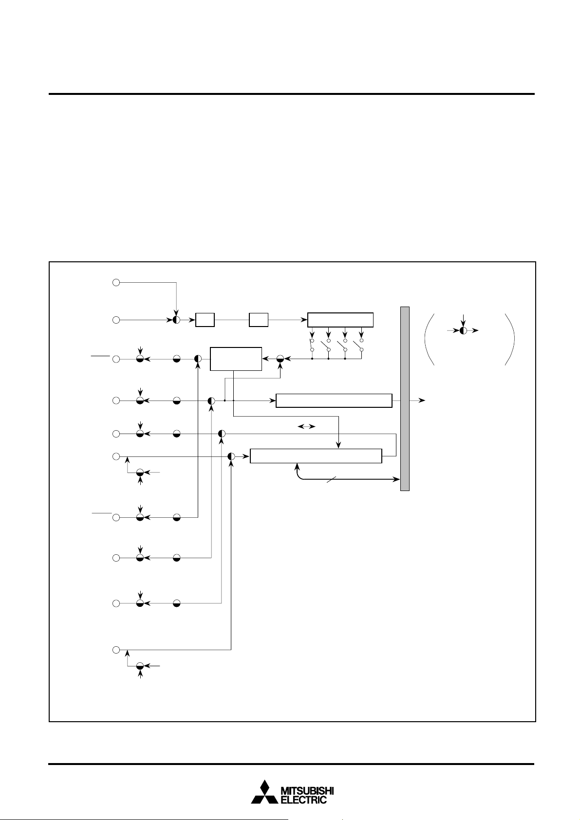
and ON-SCREEN DISPLAY CONTROLLER
Data bus
8
TMR1
5
TMR1
1/8
5
TMR1
TMR1
TMR1
TMR2
0
TMR1
4
1
TMR1
0
TMR2
Timer 1 latch (8)
2
Timer 2 latch (8)
3
Timer 3 latch(8)
2
8
Timer 1 (8)
8
Timer 2 (8)
8
Timer 3 (8)
Timer 1
interrupt request
8
8
Timer 2
interrupt request
8
8
FF
16
Reset
STP instruction
Timer 3
interrupt request
8
8
07
16
8
8
Selection gate : Connected to
black side at
reset.
TMR2
TMR2
4
TMR2
1
Timer 4 latch (8)
3
TMR1
6
Timer 5 latch (8)
8
Timer 4 (8)
8
Timer 5 (8)
7
TMR1 : Timer mode register 1
TMR2 : Timer mode register 2
TMR3 : Timer mode register 3
CM : CPU mode register
TMR2
TMR3
TMR2
0
5
8
8
Timer 6 latch (8)
8
TMR1
7
TMR2
Timer 6 (8)
6
8
Notes 1: HIGH pulse width of external clock inputs TIM2 and TIM3 needs 4 machine cycles or more.
2: When the external clock source is selected, timers 1, 2, and 3 are counted at a rising edge of input signal.
3: In the stop mode or the wait mode, external clock inputs TIM2 and TIM3 cannot be used.
Timer 4
interrupt request
Timer 5
interrupt request
Timer 6
interrupt request
Fig. 17. Timer Block Diagram
24
Page 25
MITSUBISHI MICROCOMPUTERS
M37207MF-XXXSP/FP, M37207M8-XXXSP
M37207EFSP/FP
SINGLE-CHIP 8-BIT CMOS MICROCOMPUTER for VOLTAGE SYNTHESIZER
and ON-SCREEN DISPLAY CONTROLLER
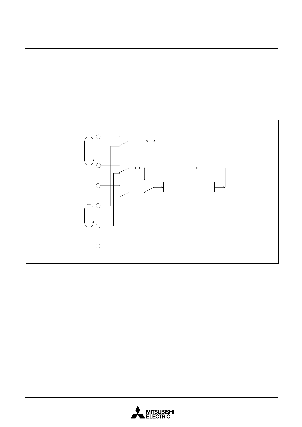
SERIAL I/O
This microcomputer has a built-in serial I/O which can either transmit
or receive 8-bit data serially in clock synchronous mode.
The serial I/O block diagram is shown in Figure 18. The synchronous
clock I/O pin (SCLK), and data I/O pins (SOUT, SIN), receive enable
signal output pin (SRDY) also function as port P4.
Bit 2 of the serial I/O mode register (address 00DE16) selects whether
the synchronous clock is supplied internally or externally (from the
pins SCLK1, SCLK2). When an internal clock is selected, bits 1 and 0
select whether f(XIN) or f(XCIN) is divided by 8, 16, 32, or 64. To use
pins for serial I/O, set the corresponding bits of the port P4 direction
register (address 00C916) to “0.”
S
S
S
S
S
X
CIN
X
RDY2
CLK2
OUT2
IN2
S
RDY1
CLK1
IN
____
P43 latch
SM4
P41 latch
SM3
P40 latch
SM3
SM6
0
latch
P4
P47 latch
SIC7
P45 latch
SIC5
CM7
SCL2 CSIO
SM6
SCL3
SM7
SDA3
SM7
SDA2
PWM8
SIC3
SCL1
SIC4
1/2
CSIO
CSIO
Synchronous
circuit
CSIO
1/2
SM5
Serial I/O shift register (8)
CM : CPU mode register
SM : Serial I/O mode register
SIC : Serial I/O control register
CSIO : Bit 1 of serial I/O control register
The operation of the serial I/O is described below. The operation
differs depending on the clock source; external clock or internal clock.
Frequency divider
1/2
SM2
S
Serial I/O counter (8)
: LSB MSB
1/81/4 1/16
SM
SM
(Note)
(Address 00DF16)
8
Data bus
1
0
Selection gate : Connected to
black side at
reset.
Serial I/O
interrupt request
P44 latch
S
OUT1
S
IN1
SIC5
SIC6
PWM9
6
latch
P4
Note : When the data is set in the serial I/O register (address 00DF
Fig. 18. Serial I/O Block Diagram
SDA1
SIC4
16
), the register functions as the serial I/O shift register.
25
Page 26
MITSUBISHI MICROCOMPUTERS
M37207MF-XXXSP/FP, M37207M8-XXXSP
M37207EFSP/FP
SINGLE-CHIP 8-BIT CMOS MICROCOMPUTER for VOLTAGE SYNTHESIZER
and ON-SCREEN DISPLAY CONTROLLER
Internal clock : The SRDY signal goes to HIGH during the write cycle
by writing data into the serial I/O register (address 00DD16). After the
write cycle, the SRDY signal goes to “L” (receive enable state). The
____
SRDY signal goes to “H” at the next falling edge of the transfer clock
____
____
for the serial I/O register.
The serial I/O counter is set to “7” during write cycle into the serial I/
O register (address 00DD16), and transfer clock goes HIGH forcibly.
At each falling edge of the transfer clock after the write cycle, serial
data is output from the SOUT pin. Transfer direction can be selected
by bit 5 of the serial I/O mode register. At each rising edge of the
transfer clock, data is input from the SIN pin and data in the serial I/O
register is shifted 1 bit.
After the transfer clock has counted 8 times, the serial I/O counter
becomes “0” and the transfer clock stops at HIGH. At this time the
interrupt request bit is set to “1.”
External clock : When an external clock is selected as the clock source,
the interrupt request is set to “1” after the transfer clock has counted
8 counts. However, transfer operation does not stop, so the clock
should be controlled externally. Use the external clock of 1 MHz or
less with a duty cycle of 50%.
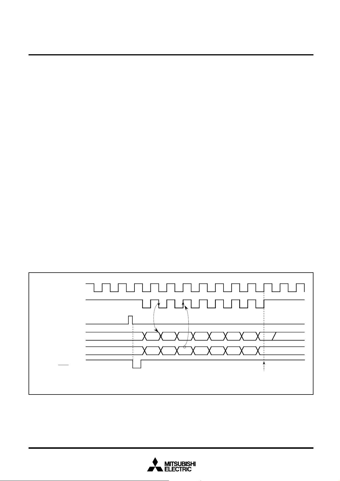
The serial I/O timing is shown in Figure 19. When using an external
clock for transfer, the external clock must be held at “H” for initializing
the serial I/O counter. When switching between an internal clock and
an external clock, do not switch during transfer. Also, be sure to initialize the serial I/O counter after switching.
Notes 1: On programming, note that the serial I/O counter is set by
writing to the serial I/O register with the bit managing instructions such as SEB and CLB.
2: When an external clock is used as the synchronous clock,
write transmit data to the serial I/O register when the transfer clock input level is HIGH.
Synchronous clock
Transfer clock
Serial I/O register
write signal
Serial I/O output
S
OUT
Serial I/O input
S
IN
Receive
signal
enable
RDY
S
Note : When an internal clock is selected, the S
Fig. 19. Serial I/O Timing (for LSB first)
D
0
D
1
D
2
D
3
D
4
D
OUT
pin is at high-impedance after transfer is completed.
(See note)
5
D
6
D
7
Interrupt request bit is set to “1”
26
Page 27
Serial I/O Mode Register
b7b6 b5b4b3 b2b1b0
MITSUBISHI MICROCOMPUTERS
M37207MF-XXXSP/FP, M37207M8-XXXSP
M37207EFSP/FP
SINGLE-CHIP 8-BIT CMOS MICROCOMPUTER for VOLTAGE SYNTHESIZER
and ON-SCREEN DISPLAY CONTROLLER
)/4 or f(X
)/16 or f(X
)/32 or f(X
)/64 or f(X
CIN
CIN
CIN
CIN
16]
)/4
)/16
)/32
)/64
After reset
0
RW
RW
Serial I/O mode register (SM) [Address 00DE
B Name Functions
Internal synchronous
0, 1
clock selection bits
(SM0, SM1)
(See note 1)
b1 b0
0 0: f(X
0 1: f(X
1 0: f(X
1 1: f(X
IN
IN
IN
IN
Fig. 20. Serial I/O Mode Register
Serial I/O Control Register
b7b6 b5b4b3 b2b1b0
Synchronous clock
2
selection bit (SM2)
0, P41
Ports P4
3, 7
function selection
bits (SM3, SM7)
(See note 2)
4, 6
Ports P4
2, P43
function selection bits
(SM4, SM6)
(See note 2)
Transfer direction
5
selection bit (SM5)
Notes 1: Either f(XIN) or f(XCIN) is selected by bit 7 of the CPU
mode register.
2: When using ports P4
the serial control register to “1.”
Serial I/O control register (SIC) [Address 0207
B Name Functions
Input signal to sift
0
register selection bit
(SIC0)
Serial I/O pin switch
1
bit (CSIO)
2
C-BUS connection
I
2
ports switch bit
(SIC2)
7
function
Ports P4
3, 7
selection bits
(SM3, SM7)
(See note 2)
4, 5
Ports P4
4
, P45
function selection bits
(SM4, SM6)
(See note 2)
6
function
Ports P4
6
selection bits
(SIC6)
(See note 2)
Notes 1: When inputting data from the S
I/O register.
2: When using ports P4
serial I/O control register to “0.”
0: External clock
1: Internal clock
b7
b3
P40/S
OUT2
/
P41/S
CLK2
CIN
SDA3/X
0
P4
✕
0
1
b6
0
1
0
1
0: LSB first
1: MSB first
0
1
S
OUT2
SDA3
b4
P42/S
IN2
/
SDA2/AD8
0
P4
2
SDA2
1
P4
2
SDA2
0–P43 as serial I/O pins, set bit 1 of
COUT
SCL3/X
P4
1
S
CLK2
SCL3
P43/S
RDY2
SCL2/AD7
P4
3
S
RDY2
SDA2
16
]
/
/
After reset
CSIO b0
0 0: Input signal from S
0 1: Input signal from S
1 0: Input signal from S
1 1: Input signal from S
0:
S
OUT1
,
S
CLK1
1:
S
OUT2
,
S
CLK2
0:
SDA2, SCL2, SDA1, SCL1
1:
SDA3, SCL3
P47/S
b7
b3
0
✕
1
0
1
b5
b4
P44/S
OUT1
SDA1
0
P4
4
✕
1
S
OUT1
0
1
SDA1
b6
P46/S
0
1
out
4
–P47 as serial I/O pins, set bit 1 of the
IN1
OUT1
(See note 1)
IN2
OUT2
(See note 1)
,
S
IN1
,
S
RDY1
,
S
IN2
,
S
RDY2
RDY1
/PWM8
P4
7
S
RDY1
PWM8
/
P45/S
CLK1
/
SCL1
P4
5
S
CLK1
SCL1
IN1
/PWM9
P4
6
PWM9
pin, set “FF16” to the serial
0
RW
0
RW
0RW
0RW
RW
RW
0
RW
0
0RW
0RW
0RW
0RW
Fig. 21. Serial I/O Control Register
27
Page 28
M37207MF-XXXSP/FP, M37207M8-XXXSP
SINGLE-CHIP 8-BIT CMOS MICROCOMPUTER for VOLTAGE SYNTHESIZER
Serial I/O Common Transmission/Reception Mode
By writing “1” to bit 0 of the serial I/O control register, signals SIN and
SOUT are switched internally to be able to transmit or receive the
serial data.
Figure 22 shows signals on serial I/O common transmission/reception mode.
Note : When receiving the serial data after writing “FF16” to the serial
I/O register.
MITSUBISHI MICROCOMPUTERS
M37207EFSP/FP
and ON-SCREEN DISPLAY CONTROLLER
S
CLK2
S
OUT2
S
IN2
S
CLK1
S
OUT1
S
IN1
Fig. 22. Signals on Serial I/O Common Transmission/Reception Mode
“1”
“0”
CSIO
“1”
“0”
“1”
“0”
CSIO
“1”
“0”
SIC0
SIC0
: Bit 0 of serialI/O control register
CSIO : Bit 1 of serial I/O control register
Clock
Serial I/O shift register (8)
28
Page 29
MITSUBISHI MICROCOMPUTERS
M37207MF-XXXSP/FP, M37207M8-XXXSP
M37207EFSP/FP
SINGLE-CHIP 8-BIT CMOS MICROCOMPUTER for VOLTAGE SYNTHESIZER
and ON-SCREEN DISPLAY CONTROLLER
MULTI-MASTER I2C-BUS INTERFACE
The multi-master I2C-BUS interface is a serial communications circuit, conforming to the Philips I2C-BUS data transfer format. This
interface, offering both arbitration lost detection and a synchronous
functions, is useful for the multi-master serial communications.
Figure 23 shows a block diagram of the multi-master I2C-BUS interface and Table 2 shows multi-master I2C-BUS interface functions.
This multi-master I2C-BUS interface consists of the I2C address register, the I2C data shift register, the I2C clock control register, the I2C
control register, the I2C status register and other control circuits.
I2C address register (S0D)
b7 b0
SAD6 SAD5 SAD4 SAD3 SAD2 SAD1 SAD0 RBW
Table 2. Multi-master I2C-BUS Interface Functions
Item
Function
In conformity with Philips I2C-BUS
standard:
Format
10-bit addressing format
7-bit addressing format
High-speed clock mode
Standard clock mode
In conformity with Philips I2C-BUS
standard:
Communication mode
Master transmission
Master reception
Slave transmission
Slave reception
SCL clock frequency
16.1 kHz to 400 kHz (at φ = 4 MHz)
φ : System clock = f(XIN)/2
Note: We are not responsible for any third party’s infringement of
patent rights or other rights attributable to the use of the control function (bits 6 and 7 of the I2C control register at address
00F916) for connections between the I2C-BUS interface and
ports (SCL1, SCL2, SDA1, SDA2).
Interrupt
generating
circuit
Interrupt
request signal
(IICIRQ)
Address comparator
Serial
data
(SDA)
Noise
elimination
circuit
Data
control
circuit
b7
I C data shift register
S0
AL
circuit
BB
circuit
Serial
clock
(SCL)
Noise
elimination
circuit
Clock
control
circuit
b7 b0
FAST
ACK
ACK
I2C clock control register (S2)
BIT
MODE
Fig. 23. Block Diagram of Multi-master I2C-BUS Interface
2
CCR4 CCR3 CCR2 CCR1 CCR0
Clock division
b0
Internal data bus
System clock
b7
MST TRX BB PIN
AL AAS AD0 LRB
2
I C status
(S1)
register
b7 b0
BSEL1 BSEL0
10BIT
ALS
SAD
I2C clock control register (S1D)
(φ)
BC2 BC1 BC0
ESO
Bit counter
b0
29
Page 30
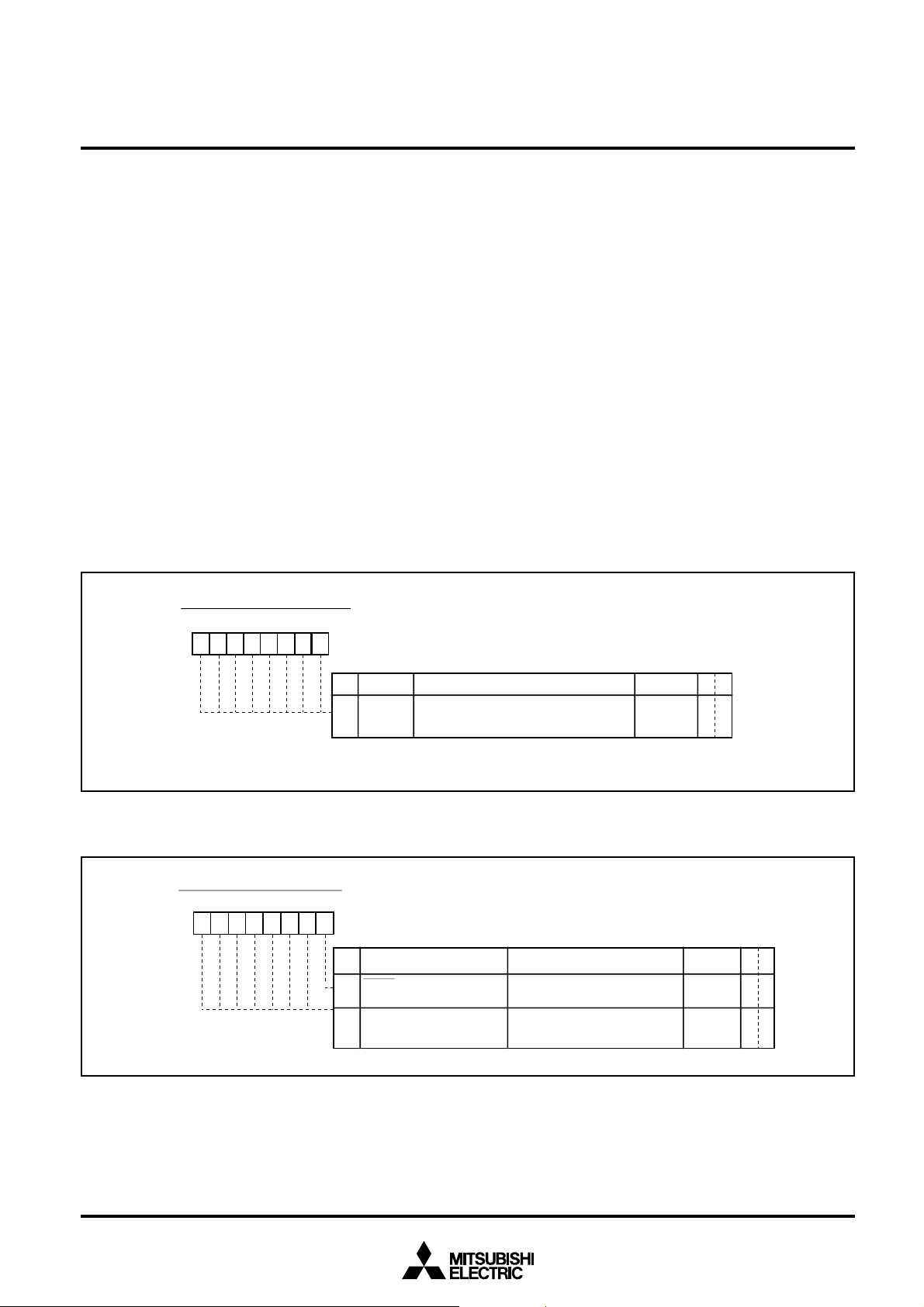
MITSUBISHI MICROCOMPUTERS
M37207MF-XXXSP/FP, M37207M8-XXXSP
M37207EFSP/FP
SINGLE-CHIP 8-BIT CMOS MICROCOMPUTER for VOLTAGE SYNTHESIZER
and ON-SCREEN DISPLAY CONTROLLER
(1) I2C Data Shift Register
The I2C data shift register (S0 : address 00D916) is an 8-bit shift
register to store receive data and write transmit data.
When transmit data is written into this register, it is transferred to the
outside from bit 7 in synchronization with the SCL clock, and each
time one-bit data is output, the data of this register are shifted one bit
to the left. When data is received, it is input to this register from bit 0
in synchronization with the SCL clock, and each time one-bit data is
input, the data of this register are shifted one bit to the left.
The I2C data shift register is in a write enable status only when the
ESO bit of the I2C control register (address 00DC16) is “1.” The bit
counter is reset by a write instruction to the I2C data shift register.
When both the ESO bit and the MST bit of the I2C status register
(address 00F816) are “1,” the SCL is output by a write instruction to
the I2C data shift register. Reading data from the I2C data shift register is always enabled regardless of the ESO bit value.
Note: To write data into the I2C data shift register after setting the
MST bit to “0” (slave mode), keep an interval of 8 machine
cycles or more.
2
I C Data Shift Register
b7 b6 b5 b4 b3 b2 b1 b0
2
I C data shift register1(S0) [Address 00D916]
(2) I2C Address Register
The I2C address register (address 00DA16) consists of a 7-bit slave
address and a read/write bit. In the addressing mode, the slave address written in this register is compared with the address data to be
received immediately after the START condition are detected.
■ Bit 0: Read/Write Bit (RBW)
Not used when comparing addresses, in the 7-bit addressing mode.
In the 10-bit addressing mode, the first address data to be received
is compared with the contents (SAD6 to SAD0 + RBW) of the I2C
address register.
The RBW bit is cleared to “0” automatically when the stop condition
is detected.
■ Bits 1 to 7: Slave Address (SAD0–SAD6)
These bits store slave addresses. Regardless of the 7-bit addressing mode and the 10-bit addressing mode, the address data transmitted from the master is compared with the contents of these bits.
___
____
Fig. 24. I2C Data Shift Register
I2C Address Register
b7 b6 b5 b4 b3 b2 b1 b0
Fig. 25. I2C Address Register
B Functions After reset R W
Name
D0 to D7
0
to
7
Note:
To write data into the I C data shift register after setting the MST bit to
“0” (slave mode), keep an interval of 8 machine cycles or more.
This is an 8-bit shift register to store
receive data and write transmit data.
2
I2C address register (S0D) [Address 00DA
B Name Functions
0
Read/write bit
(RBW)
1
Slave address
to
(SAD0 to SAD6)
7
0: Read
1: Write
the master is compared with the
contents of these bits.
16
]
Indeterminate
After reset
RW
0
0The address data transmitted from
RW
R—
RW
30
Page 31

MITSUBISHI MICROCOMPUTERS
M37207MF-XXXSP/FP, M37207M8-XXXSP
M37207EFSP/FP
SINGLE-CHIP 8-BIT CMOS MICROCOMPUTER for VOLTAGE SYNTHESIZER
and ON-SCREEN DISPLAY CONTROLLER
(3) I2C Clock Control Register
The I2C clock control register (address 00DD16) is used to set ACK
control, SCL mode and SCL frequency.
■ Bits 0 to 4: SCL Frequency Control Bits (CCR0–CCR4)
These bits control the SCL frequency. Refer to Figure 26.
■ Bit 5: SCL Mode Specification Bit (FAST MODE)
This bit specifies the SCL mode. When this bit is set to “0,” the standard clock mode is set. When the bit is set to “1,” the high-speed
clock mode is set.
■ Bit 6: ACK Bit (ACK BIT)
This bit sets the SDA status when an ACK clock✽ is generated. When
this bit is set to “0,” the ACK return mode is set and SDA goes to
LOW at the occurrence of an ACK clock. When the bit is set to “1,”
the ACK non-return mode is set. The SDA is held in the HIGH status
at the occurrence of an ACK clock.
However, when the slave address matches the address data in the
reception of address data at ACK BIT = “0,” the SDA is automatically
made LOW (ACK is returned). If there is a mismatch between the
slave address and the address data, the SDA is automatically made
HIGH (ACK is not returned).
✽ACK clock: Clock for acknowledgement
■ Bit 7: ACK Clock Bit (ACK)
This bit specifies a mode of acknowledgment which is an acknowledgment response of data transmission. When this bit is set to “0,”
the no ACK clock mode is set. In this case, no ACK clock occurs
after data transmission. When the bit is set to “1,” the ACK clock
mode is set and the master generates an ACK clock upon completion of each 1-byte data transmission.The device for transmitting
address data and control data releases the SDA at the occurrence of
an ACK clock (make SDA HIGH) and receives the ACK bit generated by the data receiving device.
2
Note: Do not write data into the I
C clock control register during
transmission. If data is written during transmission, the I2C
clock generator is reset, so that data cannot be transmitted
normally.
I2C Clock Control Register
b7 b6 b5 b4 b3 b2 b1 b0
Fig. 26. I2C Clock Control Register
2
C clock control register (S2 : address 00DD16)
I
B Name Functions
0
SCL frequency control bits
to
(CCR0 to CCR4)
4
56SCL mode
specification bit
(FAST MODE)
ACK bit
(ACK BIT)
7
ACK clock bit
(ACK)
Note: At 400 kHz in the high-speed clock mode, the duty is as below .
“0” period : “1” period = 3 : 2
In the other cases, the duty is as below.
“0” period : “1” period = 1 : 1
Setup value of
CCR4–CCR0
00 to 02
0 : Standard clock mode
1 : High-speed clock mode
0 : ACK is returned.
1 : ACK is not returned.
0 : No ACK clock
1 : ACK clock
Standard clock
05
...
1D
1E
1F
mode
Setup disabled Setup disabled
Setup disabled
Setup disabled
100
83.3 16606
500/CCR value 1000/CCR value
17.2 34.5
16.6 33.3
16.1
φ
= 4 MHz, unit : kHz)
(at
High speed
clock mode
33303
25004
400 (See note)
32.3
After reset
0
0
0
0
RW
RW
RW
RW
RW
31
Page 32

MITSUBISHI MICROCOMPUTERS
M37207MF-XXXSP/FP, M37207M8-XXXSP
M37207EFSP/FP
SINGLE-CHIP 8-BIT CMOS MICROCOMPUTER for VOLTAGE SYNTHESIZER
and ON-SCREEN DISPLAY CONTROLLER
(4) I2C Control Register
The I2C control register (address 00DC16) controls the data communication format.
■ Bits 0 to 2: Bit Counter (BC0–BC2)
These bits decide the number of bits for the next 1-byte data to be
transmitted. An interrupt request signal occurs immediately after the
number of bits specified with these bits are transmitted.
When a START condition is received, these bits become “0002” and
the address data is always transmitted and received in 8 bits.
■ Bit 3: I2C Interface Use Enable Bit (ESO)
This bit enables usage of the multimaster I2C BUS interface. When
this bit is set to “0,” the use disable status is provided, so the SDA
and the SCL become high-impedance. When the bit is set to “1,” use
of the interface is enabled.
When ESO = “0,” the following is performed.
PIN = “1,” BB = “0” and AL = “0” are set (they are bits of the I2C
•
status register at address 00F816 ).
Writing data to the I2C data shift register (address 00F616) is dis-
•
abled.
■ Bit 4: Data Format Selection Bit (ALS)
This bit decides whether or not to recognize slave addresses. When
this bit is set to “0,” the addressing format is selected, so that address data is recognized. When a match is found between a slave
address and address data as a result of comparison or when a general call (refer to “(5) I2C Status Register,” bit 1) is received, transmission processing can be performed. When this bit is set to “1,” the
free data format is selected, so that slave addresses are not recognized.
■ Bit 5: Addressing Format Selection Bit (10BIT SAD)
This bit selects a slave address specification format. When this bit is
set to “0,” the 7-bit addressing format is selected. In this case, only
the high-order 7 bits (slave address) of the I2C address register (address 00F716) are compared with address data. When this bit is set
to “1,” the 10-bit addressing format is selected, all the bits of the I2C
address register are compared with address data.
■
Bits 6 and 7: Connection Control Bits between I2C-BUS Interface
and Ports (BSEL0, BSEL1)
These bits controls the connection between SCL and ports or SDA
and ports (refer to Figure 28).
“0”
Multi-master
2
C-BUS
I
interface
SCL
SDA
“0”
CIIC (Note 2)
“1”
“0”
CIIC (Note 2)
“1”
“1” BSEL0
“0”
“1” BSEL1
“0”
“1” BSEL0
“0”
“1” BSEL1
SCL1/P4
SCL2/P4
SCL3/P4
SDA1/P4
SDA2/P4
SDA3/P4
5
3
1
4
2
0
Notes 1 : When using multi-master I2C-BUS interface, set bits 3 to
7 of the serial I/O mode register (address 00DE16) to “1.”
2 : CIIC is bit 2 of the serial I/O control register (address
020716) (refer to Figure 21).
I2C Control Register
b7 b6 b5 b4 b3 b2 b1 b0
Fig. 27. Connection Port Control by BSEL0 and BSEL1
2
I
C control register (S1D : address 00DC16)
B Name Functions
Bit counter
0
(Number of transmit/recieve
to
bits)
2
(BC0 to BC2)
3
2
I
C-BUS interface use
enable bit (ESO)
4 Data format selection bit
(ALS)
5
Addressing format selection
bit (10BIT SAD)
6, 7 Connection control bits
Note: When using ports P11-P14 as I C-BUS interface, the output structure changes
2
between I C-BUS interface
and ports
automatically from CMOS output to N-channel open-drain output.
b2 b1 b0
0 0 0 : 8
0 0 1 : 7
0 1 0 : 6
0 1 1 : 5
1 0 0 : 4
1 0 1 : 3
1 1 0 : 2
1 1 1 : 1
0 : Disabled
1 : Enabled
0 : Addressing mode
1 : Free data format
0 : 7-bit addressing format
1 : 10-bit addressing format
b7 b6 Connection port (See note)
0 0 : None
0 1 : SCL1, SDA1
1 0 : SCL2, SDA2
1 1 : SCL1, SDA1
SCL2, SDA2
2
After reset
0
0
0
0
0
RW
RW
RW
RW
RW
RW
Fig. 28. I2C Control Register
32
Page 33

MITSUBISHI MICROCOMPUTERS
M37207MF-XXXSP/FP, M37207M8-XXXSP
M37207EFSP/FP
SINGLE-CHIP 8-BIT CMOS MICROCOMPUTER for VOLTAGE SYNTHESIZER
and ON-SCREEN DISPLAY CONTROLLER
(5) I2C Status Register
The I2C status register (address 00DB16) controls the I2C-BUS interface status. The low-order 4 bits are read-only bits and the highorder 4 bits can be read out and written to.
■
Bit 0: Last Receive Bit (LRB)
This bit stores the last bit value of received data and can also be
used for ACK receive confirmation. If ACK is returned when an ACK
clock occurs, the LRB bit is set to “0.” If ACK is not returned, this bit
is set to “1.” Except in the ACK mode, the last bit value of received
data is input. The state of this bit is changed from “1” to “0” by executing a write instruction to the I2C data shift register (address 00D916).
■ Bit 1: General Call Detecting Flag (AD0)
This bit is set to “1” when a general call✽ whose address data is all “0”
is received in the slave mode. By a general call of the master device,
every slave device receives control data after the general call. The
AD0 bit is set to “0” by detecting the STOP condition or START condition.
✽General call: The master transmits the general call address “0016”
to all slaves.
■ Bit 2: Slave Address Comparison Flag (AAS)
This flag indicates a comparison result of address data.
In the slave receive mode, when the 7-bit addressing format is
selected, this bit is set to “1” in one of the following conditions.
The address data immediately after occurrence of a START
•
condition matches the slave address stored in the high-order
7 bits of the I2C address register (address 00DA16).
A general call is received.
•
In the slave reception mode, when the 10-bit addressing format is
selected, this bit is set to “1” with the following condition.
When the address data is compared with the I2C address
•
register (8 bits consists of slave address and RBW), the first
bytes match.
The state of this bit is changed from “1” to “0” by executing a write
instruction to the I2C data shift register (address 00D916).
■ Bit 3: Arbitration Lost✽ Detecting Flag (AL)
In the master transmission mode, when a device other than the microcomputer sets the SDA to “L,”, arbitration is judged to have been
lost, so that this bit is set to “1.” At the same time, the TRX bit is set to
“0,” so that immediately after transmission of the byte whose arbitration was lost is completed, the MST bit is set to “0.” When arbitration
is lost during slave address transmission, the TRX bit is set to “0”
and the reception mode is set. Consequently, it becomes possible to
receive and recognize its own slave address transmitted by another
master device.
✽Arbitration lost: The status in which communication as a master is
disabled.
■ Bit 4: I2C-BUS Interface Interrupt Request Bit (PIN)
This bit generates an interrupt request signal. Each time 1-byte data
is transmitted, the state of the PIN bit changes from “1” to “0.” At the
same time, an interrupt request signal is sent to the CPU. The PIN bit
is set to “0” in synchronization with a falling edge of the last clock
(including the ACK clock) of an internal clock and an interrupt request signal occurs in synchronization with a falling edge of the PIN
bit. When the PIN bit is “0,” the SCL is kept in the “0” state and clock
generation is disabled. Figure 30 shows an interrupt request signal
generating timing chart.
The PIN bit is set to “1” in any one of the following conditions.
Executing a write instruction to the I2C data shift register (address
•
00F616).
When the ESO bit is “0”
•
At reset
•
The conditions in which the PIN bit is set to “0” are shown below:
Immediately after completion of 1-byte data transmission (includ-
•
ing when arbitration lost is detected)
Immediately after completion of 1-byte data reception
•
In the slave reception mode, with ALS = “0” and immediately after
•
completion of slave address or general call address reception
In the slave reception mode, with ALS = “1” and immediately after
•
completion of address data reception
33
Page 34

MITSUBISHI MICROCOMPUTERS
M37207MF-XXXSP/FP, M37207M8-XXXSP
M37207EFSP/FP
SINGLE-CHIP 8-BIT CMOS MICROCOMPUTER for VOLTAGE SYNTHESIZER
and ON-SCREEN DISPLAY CONTROLLER
■ Bit 5: Bus Busy Flag (BB)
This bit indicates the status of use of the bus system. When this bit is
set to “0,” this bus system is not busy and a START condition can be
generated. When this bit is set to “1,” this bus system is busy and the
occurrence of a START condition is disabled by the START condition duplication prevention function (Note).
This flag can be written by software only in the master transmission
mode. In the other modes, this bit is set to “1” by detecting a START
condition and set to “0” by detecting a STOP condition. When the
ESO bit of the I2C control register (address 00DC16) is “0” and at
reset, the BB flag is kept in the “0” state.
■ Bit 6: Communication Mode Specification Bit (transfer direction
specification bit: TRX)
This bit decides the direction of transfer for data communication. When
this bit is “0,” the reception mode is selected and the data of a transmitting device is received. When the bit is “1,” the transmission mode
is selected and address data and control data are output into the
SDA in synchronization with the clock generated on the SCL.
When the ALS bit of the I2C control register (address 00DC16) is “0”
in the slave reception mode is selected, the TRX bit is set to “1”
(transmit) if the least significant bit (R/W bit) of the address data transmitted by the master is “1.” When the ALS bit is “0” and the R/W bit is
“0,” the TRX bit is cleared to “0” (receive).
The TRX bit is cleared to “0” in one of the following conditions.
When arbitration lost is detected.
•
When a STOP condition is detected.
•
When occurence of a START condition is disabled by the START
•
condition duplication prevention function (Note).
With MST = “0” and when a START condition is detected.
•
With MST = “0” and when ACK non-return is detected.
•
At reset
•
__
__
■ Bit 7: Communication Mode Specification Bit (master/slave specification bit: MST)
This bit is used for master/slave specification for data communication. When this bit is “0,” the slave is specified, so that a START
condition and a STOP condition generated by the master are received,
and data communication is performed in synchronization with the
clock generated by the master. When this bit is “1,” the master is
specified and a START condition and a STOP condition are generated, and also the clocks required for data communication are generated on the SCL.
The MST bit is cleared to “0” in one of the following conditions.
Immediately after completion of 1-byte data transmission when ar-
•
bitration lost is detected
When a STOP condition is detected.
•
When occurence of a START condition is disabled by the START
•
condition duplication preventing function (Note).
At reset
•
Note: The START condition duplication prevention function disables
the START condition generation, reset of bit counter reset,
and SCL output, when the following condition is satisfied:
• a START condition is set by another master device.
34
Page 35

I2C Status Register
b7 b6 b5 b4 b3 b2 b1 b0
MITSUBISHI MICROCOMPUTERS
M37207MF-XXXSP/FP, M37207M8-XXXSP
M37207EFSP/FP
SINGLE-CHIP 8-BIT CMOS MICROCOMPUTER for VOLTAGE SYNTHESIZER
and ON-SCREEN DISPLAY CONTROLLER
I2C status register (S1) [Address 00DB
16
]
Fig. 29. I2C Status Register
SCL
B Name Functions
0
Last receive bit (LRB)
(See note)
General call detecting flag
1
(AD0) (See note)
2
Slave address comparison
flag (AAS) (See note)
3
Arbitration lost detecting flag
(AL) (See note)
4
2
I
C-BUS interface interrupt
request bit (PIN)
5
Bus busy flag (BB)
6, 7 b7 b6
Communication mode
specification bits
(TRX, MST)
Note : These bits and flags can be read out, but cannnot be written.
0 : Last bit = “0 ”
1 : Last bit = “1 ”
0 : No general call detected
1 : General call detected
0 : Address mismatch
1 : Address match
0 : Not detected
1 : Detected
0 : Interrupt request issued
1 : No interrupt request issued
0 : Bus free
1 : Bus busy
0 0 : Slave recieve mode
0 1 : Slave transmit mode
1 0 : Master recieve mode
1 1 : Master transmit mode
After reset
Indeterminate
0
0
0
0
0
0
RW
R—
R—
R—
R—
R—
RW
RW
PIN
IICIRQ
Fig. 30. Interrupt Request Signal Generation Timing
35
Page 36

MITSUBISHI MICROCOMPUTERS
M37207MF-XXXSP/FP, M37207M8-XXXSP
M37207EFSP/FP
SINGLE-CHIP 8-BIT CMOS MICROCOMPUTER for VOLTAGE SYNTHESIZER
and ON-SCREEN DISPLAY CONTROLLER
(6) START Condition Generation Method
When the ESO bit of the I2C control register (address 00DC16) is “1,”
execute a write instruction to the I2C status register (address 00DB16)
to set the MST, TRX and BB bits to “1.” A START condition will then
be generated. After that, the bit counter becomes “0002” and an SCL
for 1 byte is output. The START condition generation timing and BB
bit set timing are different in the standard clock mode and the highspeed clock mode. Refer to Figure 31 for the START condition generation timing diagram, and Table 3 for the START condition/STOP
condition generation timing table.
I2C status register
write signal
SCL
SDA
BB flag
Fig. 31. START Condition Generation Timing Diagram
Setup
time
Setup
time
Hold time
Set time for
BB flag
(7) RESTART Condition Generation Method
To generate the RESTART condition, take the following sequence:
Set “2016” to the I2C status register (S1).
Write a transmit data to the I2C data shift register.
Set “F016” to the I2C status register (S1) again.
<Example of Setting of RESTART Condition>
I2C status register ; S1 = 2016
I2C data shift register ; S0 = transmit data after restart
I2C status register ; S1 = F016
Table 3. START Condition/STOP Condition Generation Timing
Table
Item
Setup time
Hold time
Set/reset time
for BB flag
Note: Absolute time at φ = 4 MHz. The value in parentheses de-
notes the number of φ cycles.
Standard Clock Mode
5.0 µs (20 cycles)
5.0 µs (20 cycles)
3.0 µs (12 cycles)
High-speed Clock Mode
2.5 µs (10 cycles)
2.5 µs (10 cycles)
1.5 µs (6 cycles)
(9) START/STOP Condition Detect Conditions
The START/STOP condition detect conditions are shown in
Figure 33 and Table 4. Only when the 3 conditions of Table 4 are
satisfied, a START/STOP condition can be detected.
Note: When a STOP condition is detected in the slave mode
(MST = 0), an interrupt request signal “IICIRQ” is generated
to the CPU.
SCL release time
SCL
SDA
(START condition)
SDA
(STOP condition)
Fig. 33. START Condition/STOP Condition Detect Timing
Diagram
Setup
time
Setup
time
Hold time
Hold time
(8) STOP Condition Generation Method
When the ES0 bit of the I2C control register (address 00DC16) is “1,”
execute a write instruction to the I2C status register (address 00DB16)
for setting the MST bit and the TRX bit to “1” and the BB bit to “0”. A
STOP condition will then be generated. The STOP condition generation timing and the BB flag reset timing are different in the standard
clock mode and the high-speed clock mode. Refer to Figure 32 for
the STOP condition generation timing diagram, and Table 3 for the
START condition/STOP condition generation timing table.
I2C status register
write signal
SCL
SDA
BB flag
Fig. 32. STOP Condition Generation Timing Diagram
36
Setup
time
Hold time
Reset time for
BB flag
Table 4. START Condition/STOP Condition Detect Conditions
Standard Clock Mode
6.5 µs (26 cycles) <
release time
3.25 µs (13 cycles) < Setup time
3.25 µs (13 cycles) < Hold time
Note: Absolute time at φ = 4 MHz. The value in parentheses de-
notes the number of φ cycles.
SCL
High-speed Clock Mode
1.0 µs (4 cycles) <
release time
0.5 µs (2 cycles) < Setup time
0.5 µs (2 cycles) < Hold time
SCL
Page 37

MITSUBISHI MICROCOMPUTERS
M37207MF-XXXSP/FP, M37207M8-XXXSP
M37207EFSP/FP
SINGLE-CHIP 8-BIT CMOS MICROCOMPUTER for VOLTAGE SYNTHESIZER
and ON-SCREEN DISPLAY CONTROLLER
(10) Address Data Communication
There are two address data communication formats, namely, 7-bit
addressing format and 10-bit addressing format. The respective address communication formats is described below.
7-bit addressing format
To meet the 7-bit addressing format, set the 10BIT SAD bit of the
I2C control register (address 00DC16) to “0.” The first 7-bit address data transmitted from the master is compared with the highorder 7-bit slave address stored in the I2C address register (address 00DA16). At the time of this comparison, address comparison of the RBW bit of the I2C address register (address 00DA16)
is not made. For the data transmission format when the 7-bit addressing format is selected, refer to Figure 34, (1) and (2).
10-bit addressing format
To meet the 10-bit addressing format, set the 10BIT SAD bit of the
I2C control register (address 00DC16) to “1.” An address comparison is made between the first-byte address data transmitted from
the master and the 7-bit slave address stored in the I2C address
register (address 00DA16). At the time of this comparison, an address comparison between the RBW bit of the I2C address register (address 00DA16) and the R/W bit which is the last bit of the
address data transmitted from the master is made. In the 10-bit
addressing mode, the R/W bit which is the last bit of the address
data not only specifies the direction of communication for control
data but also is processed as an address data bit.
When the first-byte address data matches the slave address, the
AAS bit of the I2C status register (address 00DB16) is set to “1.” After
the second-byte address data is stored into the I2C data shift register
(address 00D916), make an address comparison between the second-byte data and the slave address by software. When the address
data of the 2nd bytes matches the slave address, set the RBW bit of
the I2C address register (address 00DA16) to “1” by software. This
processing can match the 7-bit slave address and R/W data, which
are received after a RESTART condition is detected, with the value
of the I2C address register (address 00DA16). For the data transmission format when the 10-bit addressing format is selected, refer to
Figure 34, (3) and (4).
__
__
__
Set transmit data in the I2C data shift register (address 00D916).
At this time, an SCL and an ACK clock automatically occurs.
When transmitting control data of more than 1 byte, repeat step
.
Set “D016” in the I2C status register (address 00DB16). After this,
if ACK is not returned or transmission ends, a STOP condition will
be generated.
(12) Example of Slave Reception
An example of slave reception in the high-speed clock mode, at the
SCL frequency of 400 kHz, in the ACK non-return mode, using the
addressing format, is shown below.
Set a slave address in the high-order 7 bits of the I2C address
register (address 00DA16) and “0” in the RBW bit.
Set the no ACK clock mode and SCL = 400 kHz by setting “2516”
in the I2C clock control register (address 00DD16).
Set “1016” in the I2C status register (address 00DB16) and hold
the SCL at the HIGH.
Set a communication enable status by setting “4816” in the I2C
control register (address 00DC16).
When a START condition is received, an address comparison is
made.
•When all transmitted addresses are “0” (general call) :
AD0 of the I2C status register (address 00DB16) is set to “1” and
an interrupt request signal occurs.
•When the transmitted addresses match the address set in :
AAS of the I2C status register (address 00DB16) is set to “1” and
an interrupt request signal occurs.
•In the cases other than the above :
AD0 and AAS of the I2C status register (address 00DB16) are
set to “0” and no interrupt request signal occurs.
Set dummy data in the I2C data shift register (address 00D916).
When receiving control data of more than 1 byte, repeat step
When a STOP condition is detected, the communication ends.
.
(11) Example of Master Transmission
An example of master transmission in the standard clock mode, at
the SCL frequency of 100 kHz and in the ACK return mode is shown
below.
Set a slave address in the high-order 7 bits of the I2C address
register (address 00DA16) and “0” in the RBW bit.
Set the ACK return mode and SCL = 100 kHz by setting “8516” in
the I2C clock control register (address 00DD16).
Set “1016” in the I2C status register (address 00DB16) and hold
the SCL at the HIGH.
Set a communication enable status by setting “4816” in the I2C
control register (address 00DC16).
Set the address data of the destination of transmission in the highorder 7 bits of the I2C data shift register (address 00D916) and set
“0” in the least significant bit.
Set “F016” in the I2C status register (address 00DB16) to generate
a START condition. At this time, an SCL for 1 byte and an ACK
clock automatically occurs.
37
Page 38

S Slave address A Data A Data A/A PR/W
MITSUBISHI MICROCOMPUTERS
M37207MF-XXXSP/FP, M37207M8-XXXSP
M37207EFSP/FP
SINGLE-CHIP 8-BIT CMOS MICROCOMPUTER for VOLTAGE SYNTHESIZER
and ON-SCREEN DISPLAY CONTROLLER
(1) A master-transmitter transmits data to a slave-receiver
S Slave address A
(2) A master-receiver receives data from a slave-transmitter
S
(3) A master-transmitter transmits data to a slave-receiver with a 10-bit address
S
(4) A master-receiver receives data from a slave-transmitter with a 10-bit address
S : START condition P : STOP condition
A : ACK bit R/W : Read/Write bit
Sr : Restart condition
Fig. 34. Address Data Communication Format
7 bits “0” 1 to 8 bits 1 to 8 bits
R/W
7 bits “1” 1 to 8 bits 1 to 8 bits
Slave address
1st 7 bits
7 bits “0” 8 bits 1 to 8 bits
Slave address
1st 7 bits
7 bits “0” 8 bits 7 bits
R/W
R/W R/W
Data A Data AP
Slave address
A
2nd byte
Slave address
A
2nd byte
A Data
A
Sr
A Data A/A P
1 to 8 bits
Slave address
1st 7 bits
From master to slave
From slave to master
Data
1 to 8 bits
A Data
1 to 8 bits“1”
AP
38
Page 39

MITSUBISHI MICROCOMPUTERS
M37207MF-XXXSP/FP, M37207M8-XXXSP
M37207EFSP/FP
SINGLE-CHIP 8-BIT CMOS MICROCOMPUTER for VOLTAGE SYNTHESIZER
and ON-SCREEN DISPLAY CONTROLLER
PWM OUTPUT FUNCTION
This microcomputer is equipped with a 14-bit PWM (DA) and ten 8bit PWMs (PWM0–PWM9). DA has a 14-bit resolution with the minimum resolution bit width of 250 ns and a repeat period of
4096 µs (for f(XIN) = 8 MHz). PWM0–PWM9 have the same circuit
structure and an 8-bit resolution with minimum resolution bit width of
4 µs and repeat period of 1024 µs (for f(XIN) = 8 MHz).
Figure 35 shows the PWM block diagram. The PWM timing generating circuit applies individual control signals to PWM0–PWM9 using
f(XIN) divided by 2 as a reference signal.
(1) Data Setting
When outputting DA, first set the high-order 8 bits to the DA-H register (address 00CE16), then the low-order 6 bits to the DA-L register
(address 00CF16). When outputting PWM0–PWM9, set 8-bit output
data to the PWMi register (i means 0 to 9; addresses 00D016 to
00D416, 00F616 to 00FA16).
(2) Transferring Data from Registers to Latches
The data written to the 8-bit PWM register is transferred to the PWM
latch in each 8-bit PWM cycle period. For 14-bit PWM, the data is
transferred in the next high-order 8-bit period after the write. The
signals output to the PWM pins correspond to the contents of these
latches. When data in each PWM register is read, data in these
latches has already been read allowing the data output by the PWM
to be confirmed. However, bit 7 of the DA-L register indicated the
completion of the data transfer from the DA register to the DA latch.
When bit 7 is “0,” the transfer has been completed. When bit 7 is “1,”
the transfer has not yet begun.
(3) Operating of 8-bit PWM
The following explains PWM operation.
First, set the bit 0 of PWM output control register 1 (address 00D516)
to “0” (at reset, bit 0 is already set to “0” automatically), so that the
PWM count source is supplied.
PWM0–PWM7 are also used as pins P60–P67, PWM8, PWM9 are
also used as ports pins P47, P46, respectively. For PWM0–PWM9,
set the corresponding bits of the ports P4 or P6 direction register to
“1” (output mode). And select each output polarity by bit 3 of PWM
output control register 2(address 00D616). Then, for PWM0–PWM5,
set bits 2 to 7 of PWM output control register 1 to “1” (PWM output).
For PWM6 and PWM7, set bits 0 and 1 of the PWM output control
register 2 to “1.” For PWM8 and PWM9, set bits 3, 6 and 7 of the
serial I/O control register to “1.”
The PWM waveform is output from the PWM output pins by setting
these registers.
Figure 36 shows the 8-bit PWM timing. One cycle (T) is composed
of 256 (28) segments. The 8 kinds of pulses, relative to the weight of
each bit (bits 0 to 7), are output inside the circuit during 1 cycle.
Refer to Figure 36 (a). The 8-bit PWM outputs waveform which is
the logical sum (OR) of pulses corresponding to the contents of bits
0 to 7 of the 8-bit PWM register. Several examples are shown in
Figure 36 (b). 256 kinds of output (HIGH area: 0/256 to 255/256) are
selected by changing the contents of the PWM register. A length of
entirely HIGH output cannot be output, i.e. 256/256.
(4) Operating of 14-bit PWM
As with 8-bit PWM, set the bit 0 of PWM output control register 1
(address 00D516) to “0” (at reset, bit 0 is already set to “0” automatically), so that the PWM count source is supplied. Next, select the
output polarity by bit 2 of PWM output control register 2 (address
00D616). Then, the 14-bit PWM outputs from the D-A output pin by
setting bit 1 of PWM output control register 1 to “0” (at reset, this bit
already set to “0” automatically) to select the DA output.
The output example of the 14-bit PWM is shown in Figure 37.
The 14-bit PWM divides the data of the DA latch into the low-order 6
bits and the high-order 8 bits.
The fundamental waveform is determined with the high-order 8-bit
data “DH.” A HIGH area with a length τ ✕ DH (HIGH area of funda-
mental waveform) is output every short area of “t” = 256τ =
64 µs (τ is the minimum resolution bit width of 250 ns). The “H” level
area increase interval (tm) is determined with the low-order 6-bit data
“DL.” The HIGH are of smaller intervals “tm” shown in Table 5 is longer
by τ than that of other smaller intervals in PWM repeat period “T” =
64t. Thus, a rectangular waveform with the different HIGH width is
output from the D-A pin. Accordingly, the PWM output changes by τ
unit pulse width by changing the contents of the DA-H and DA-L
registers. A length of entirely HIGH cannot be output, i. e. 256/256.
(5) Output after Reset
At reset, the output of ports P60–P67, P46 and P47 are in the highimpedance state, and the contents of the PWM register and the
PWM circuit are undefined. Note that after reset, the PWM output is
undefined until setting the PWM register.
39
Page 40

M37207MF-XXXSP/FP, M37207M8-XXXSP
SINGLE-CHIP 8-BIT CMOS MICROCOMPUTER for VOLTAGE SYNTHESIZER
Table 5. Relation Between the Low-order 6-bit Data and High-
level Area Increase Interval
Low-order 6 bits of Data
0 0 0 0 0 0
0 0 0 0 0 1
0 0 0 0 1 0
0 0 0 1 0 0
0 0 1 0 0 0
0 1 0 0 0 0
1 0 0 0 0 0
Area Longer by τ than That of Other tm (m = 0 to 63)
LSB
Nothing
m = 32
m = 16, 48
m = 8, 24, 40, 56
m = 4, 12, 20, 28, 36, 44, 52, 60
m =
2, 6, 10, 14, 18, 22, 26, 30, 34, 38, 42, 46, 50, 54, 58, 62
m = 1, 3, 5, 7,................................. 57, 59, 61, 63
Data bus
DA-H register
(Address : 00CE
16
)
DA-L register
(Address : 00CF
b7
b0b7
MITSUBISHI MICROCOMPUTERS
M37207EFSP/FP
and ON-SCREEN DISPLAY CONTROLLER
16
)
b5 b0
Selection gate :
Connected to black
side at reset.
Pass gate
Inside of is as same contents with
the others.
PW : PWM output countrol register 1
PN : PWM output control register 2
D6 : Port P6 direction register
D4 : port P4 direction register
SIC : Serial I/O control register
DA latch (14-bits)
MSB
8
X
IN
1/2
PWM0 register
(Address : 00D0
b7
PWM0 latch
MSB
8
8-bit PWM circuit
PW0
16
)
14
7
14-bit PWM circuit
Timing
generator
for PWM
b0
LSB
PWM1 register (Address : 00D116)
PWM2 register (Address : 00D216)
PWM3 register (Address : 00D3
PWM4 register (Address : 00D4
PWM5 register (Address : 00F6
PWM6 register (Address : 00F7
PWM7 register (Address : 00F8
PWM8 register (Address : 00F9
PWM9 register (Address : 00FA
16
)
16
)
16
)
16
)
16
)
16
)
16
)
LSB
RDY1
0
1
2
3
4
5
6
7
6
PN4
PW1
P4
SIC
A-D
D-A
D-A/AD3
D6
0
D6
1
D6
2
D6
3
D6
4
D6
5
D6
6
D6
7
7
D4
7
D4
PWM0
PWM1
PWM2
PWM3
PWM4
PWM5
PWM6
PWM7
7
6
PWM8
PWM9
6
PN2
PN
3
P6
PW2
P6
PW3
P6
PW4
P6
PW5
P6
PW6
P6
PW7
P6
PN0
P6
PN1
S
SIC3
P4
SIC6
Fig. 35. PWM Block Diagram
40
Page 41
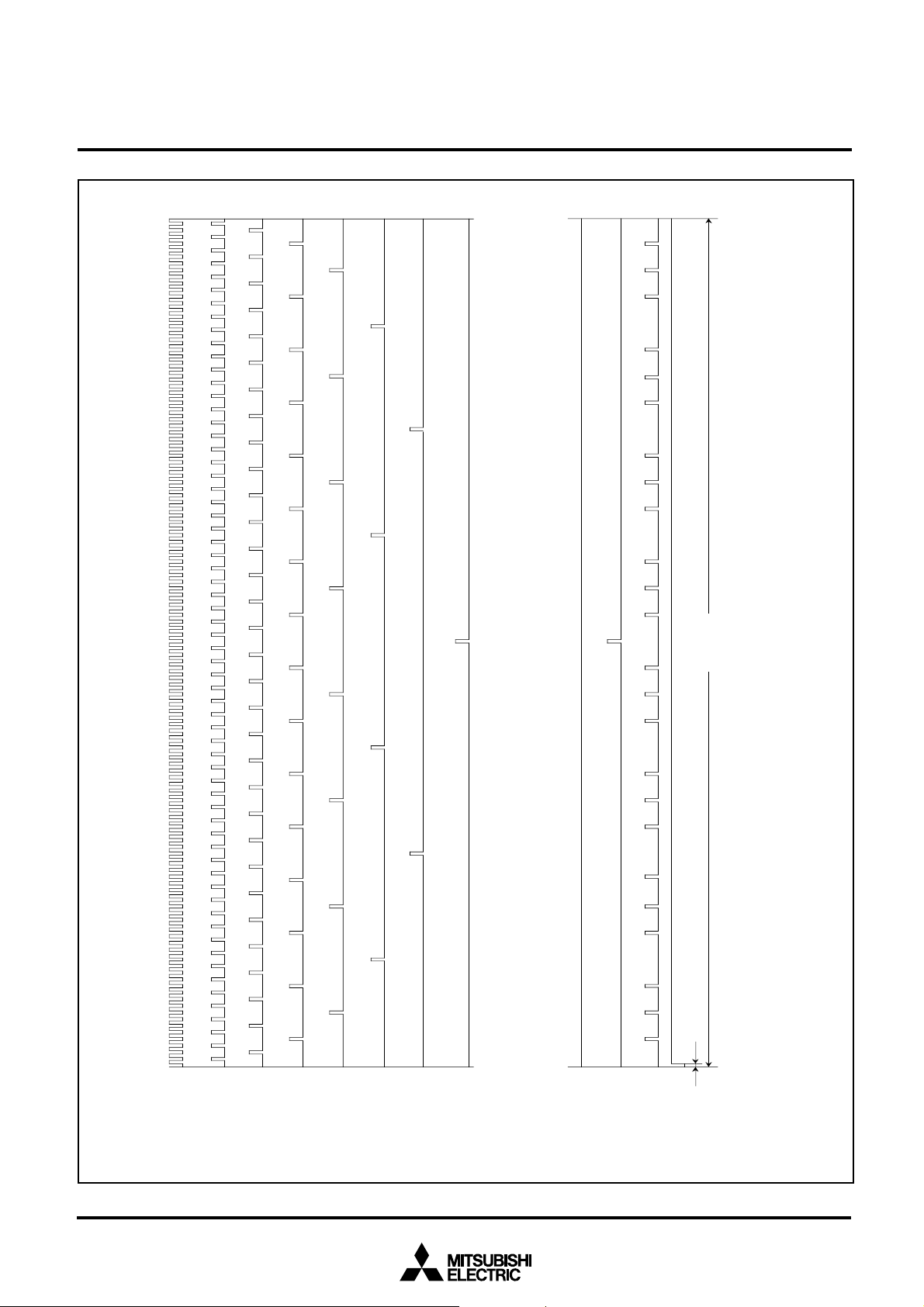
255
250
240
230
220
210
200
190
180
170
160
150
140
130
120
110
100
90
80
70
60
50
40
30
20
9
7
5
3
1
MITSUBISHI MICROCOMPUTERS
M37207MF-XXXSP/FP, M37207M8-XXXSP
M37207EFSP/FP
SINGLE-CHIP 8-BIT CMOS MICROCOMPUTER for VOLTAGE SYNTHESIZER
and ON-SCREEN DISPLAY CONTROLLER
254
252
250
246
242
238
234
230
226
222
218
214
210
206
202
198
194
190
186
182
178
174
170
166
162
158
154
150
146
142
138
134
130
126
122
118
114
110
106
102
98
94
90
86
82
78
74
70
66
62
58
54
50
46
42
38
34
30
26
22
18
14
10
6
2
244
228
212
204
196
188
172
164
156
148
132 140
124
108
100
92
84
76
68
60
52
44
20
12
4
236
220
180
116
36
28
248
232
216
200
184
168
152
136
120
104
88
72
56
40
24
8
240
208
176
144
112
80
48
16
224
160
96
32
192
s
µ
128
s T = 1024
IN) = 8 MHz
T = 256 t
µ
f(X
t = 4
(b) Example of 8-bit PWM
(a) Pulses showing the weight of each bit
PWM output
64
t
Bit 7
Fig. 36. 8-bit PWM Timing
Bit 6
Bit 5
Bit 4
Bit 3
Bit 2
Bit 1
Bit 0
16 (0)
00
16 (1)
01
16 (24)
18
FF16 (255)
41
Page 42

[DA-H
register]
Set “2C
16
” to DA-H register.
b7 b0b6 b5 b4 b3 b2 b1
0
At writing of DA-L
MITSUBISHI MICROCOMPUTERS
M37207MF-XXXSP/FP, M37207M8-XXXSP
M37207EFSP/FP
SINGLE-CHIP 8-BIT CMOS MICROCOMPUTER for VOLTAGE SYNTHESIZER
and ON-SCREEN DISPLAY CONTROLLER
16
” to DA-L register.
Latch transfer complete bit
Transfer complete
0
1
Transfer is not completed
(Automatically set at writing)
H
D
0010110
[DA-L register]
At writing of DA-L
Set “28
b7
Undefined
b0b6 b5 b4 b3 b2 b1
D
L
010100
b13 b6
[DA latch]
“H” level area of
fundamental waveform
Fundamental
waveform
14-bit
PWM output
8-bit
counter
Fundamental waveform of smaller interval
“tm” which is not specified by low-order 6
bits is not changed.
14-bit PWM output
Low-order 6-bit
output of DA latch
=
250 ns✕44
2C 2B 2A … 03 02 01 00 2C 2B 2A … 03 02 01 002D 2D
FF 00D3FE FD
0
These bits decide “H” level area of
fundamental waveform.
Minimum
resolution bit
width 250 ns
…
D6 D4 02 01D5
b0b5
0010110
101000
These bits decide smaller interval “tm” in which “H” leval
area is [“H” level area of fundamental waveform + τ ].
High-order 8-bit
✕
value of DA latch
Waveform of smaller interval “tm” specified by low-order 6 bits
250 ns✕44
14-bit
PWM output
………
250 ns✕44
t
0t1t2t3t4t5
8-bit
counter
τ = 250 ns
Repeat period
T = 4096 µ
FF 00D3FE FD D6 D4 02 01D5
t59t
60t61t62t63
s
250 ns
Fig. 37. 14-bit PWM (DA) Output Example (at f(XIN) = 8 MHz)
42
Page 43

PWM Output Control Register 1
b7b6 b5b4b3 b2b1b0
PWM output control register 1 (PW) [Address 00D5
MITSUBISHI MICROCOMPUTERS
M37207MF-XXXSP/FP, M37207M8-XXXSP
M37207EFSP/FP
SINGLE-CHIP 8-BIT CMOS MICROCOMPUTER for VOLTAGE SYNTHESIZER
and ON-SCREEN DISPLAY CONTROLLER
16
]
Fig. 38. PWM Output Control Register 1
PWM Output Control Register 2
B
0
Name Functions
DA, PWM count source
selection bit (PW0)
1
DA/PN4 output
selection bit (PW1)
P60/PWM0 output
2
selection bit (PW2)
P6
1
/PWM1 output
3
selection bit (PW3)
P6
2
/PWM2 output
4
selection bit (PW4)
P6
3
/PWM3 output
5
selection bit (PW5)
4
/PWM4 output
P6
6
selection bit (PW6)
5
/PWM5 output
P6
7
selection bit (PW7)
0 : Count source supply
1 : Count source stop
0 : DA output
1 : PN4 output
0: P6
0
output
1: PWM0 output
0: P6
1
output
1: PWM1 output
0: P6
2
output
1: PWM2 output
0: P6
3
output
1: PWM3 output
0: P6
4
output
1: PWM4 output
0: P6
5
output
1: PWM5 output
After reset
0
0
0
0
0
0
0
0
RW
RW
RW
RW
RW
RW
RW
RW
RW
b7b6 b5b4b3 b2b1b0
Fig. 39. PWM Output Control Register 2
PWM output control register 2 (PN) [Address 00D6
B
P6
0
selection bit (PN0)
P6
1
selection bit (PN1)
DA output polarity
2
selection bit (PN3)
PWM output polarity
3
selection bit (PN4)
DA general-purpose
4
output bit (PN5)
5
Nothing is assigned. These bits are write disable bits.
to
When these bits are read out, the values are “0.”
Name Functions
6
/PWM6 output
0 : P6
6
output
1 : PWM6 output
7
/PWM7 output
0 : P6
7
output
1 : PWM7 output
0 : Positive polarity
1 : Negative polarity
0 : Positive polarity
1 : Negative polarity
0 : Output LOW
1 : Output HIGH
7
16
]
After reset
RW
0RW
0RW
0
RW
0
RW
0
RW
0
R—
43
Page 44
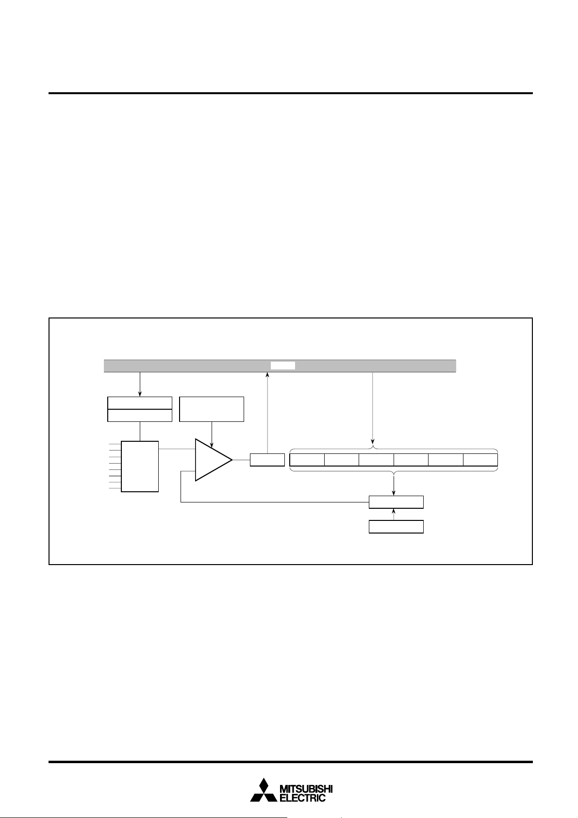
M37207MF-XXXSP/FP, M37207M8-XXXSP
SINGLE-CHIP 8-BIT CMOS MICROCOMPUTER for VOLTAGE SYNTHESIZER
A-D COMPARATOR
A-D comparator consists of 6-bit D-A converter and comparator. A-D
comparator block diagram is shown in Figure 40.
The reference voltage “Vref” for D-A conversion is set by bits 0 to 5 of
the A-D control register 2 (address 020A16).
The comparison result of the analog input voltage and the reference
voltage “Vref” is stored in bit 4 of the A-D control register 1 (address
00EF16).
For A-D comparison, set “0” to corresponding bits of the direction
register to use ports as analog input pins. Write the data for select of
analog input pins to bits 0 to 2 of the A-D control register 1 and write
the digital value corresponding to Vref to be compared to the bits 0 to
5 A-D control register 2. The voltage comparison starts by writing to
the A-D control register 2, and it is completed after 16 machine cycles
(NOP instruction ✕ 8).
MITSUBISHI MICROCOMPUTERS
M37207EFSP/FP
and ON-SCREEN DISPLAY CONTROLLER
A-D control register 1
Bits 0 to 2
AD1
AD2
AD3
AD4
AD5
AD6
AD7
AD8
Analog
signal
switch
Comparator control
Fig. 40. A-D Comparator Block Diagram
Comparator
Data bus
A-D control register 1
Bit 4
A-D control register 2
Bit 5 Bit 4 Bit 3 Bit 2 Bit 1 Bit 0
Switch tree
Resistor ladder
44
Page 45
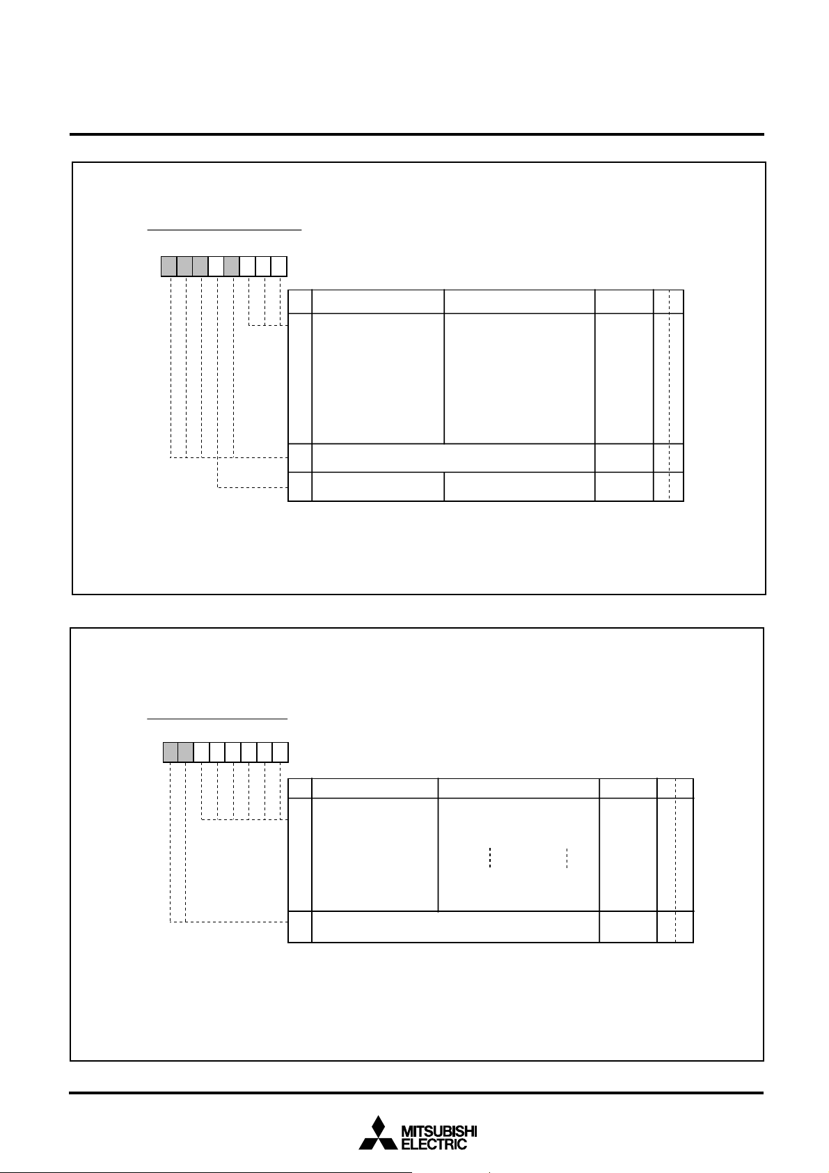
A-D Control Register 1
b7 b6 b5 b4 b3 b2 b1 b0
MITSUBISHI MICROCOMPUTERS
M37207MF-XXXSP/FP, M37207M8-XXXSP
M37207EFSP/FP
SINGLE-CHIP 8-BIT CMOS MICROCOMPUTER for VOLTAGE SYNTHESIZER
and ON-SCREEN DISPLAY CONTROLLER
A-D control register 1 (ADM) [Address 00EF16]
Fig. 41. A-D Control Register 1
B
0
Analog input pin selection
to
bits
2
(ADM0 to ADM2)
Nothing is assigned. These bits are write disable bits.
3,
When these bits are read out, the values are “0.”
5
to
7
Storage bit of comparison
4
result (ADM4)
Name Functions
b2 b1 b0
0 0 0 : AD1
0 0 1 : AD2
0 1 0 : AD3
0 1 1 : AD4
1 0 0 : AD5
1 0 1 : AD6
1 1 0 : AD7
1 1 1 : AD8
0:
Input voltage < reference voltage
1:
Input voltage > reference voltage
After reset
0
0
Indeterminate
RW
RW
R—
R—
A-D Control Register 2
b7 b6 b5 b4 b3 b2 b1 b0
Fig. 42. A-D Control Register 2
A-D control register 2(ADC) [Address 020A
B
D-A converter set bits
0
(ADC0 to ADC5)
to
5
Nothing is assigned. These bits are write disable bits.
6, 7
When these bits are reed out, the values are “ 0.”
Name Functions
16
000000
00000
000000
1
11111
11111
111111
]
b0b1b2 b3 b4 b5
1
0
: 1/128Vcc
: 3/128Vcc
: 5/128Vcc
: 123/128Vcc
: 125/128Vcc
: 127/128Vcc
After reset
Indeterminate
RW
RW
R—
0
45
Page 46

M37207MF-XXXSP/FP, M37207M8-XXXSP
SINGLE-CHIP 8-BIT CMOS MICROCOMPUTER for VOLTAGE SYNTHESIZER
CRT DISPLAY FUNCTIONS
(1) Outline of CRT Display Functions
Table 6 outlines the CRT display functions of this microcomputer.
This microcomputer incorporates a CRT display circuit of 24 characters ✕ 3 lines. CRT display is controlled by the CRT control register.
Up to 256 kinds of characters can be displayed. The colors can be
specified for each character and up to 4 kinds of colors can be displayed on one screen. A combination of up to 15 colors can be obtained by using each output signal (R, G, B and I).
Characters are displayed in a 12 ✕ 16 dots configuration to obtain
smooth character patterns (refer to Figure 43).
The following shows the procedure how to display characters on the
CRT screen.
Write the display character code in the display RAM.
Specify the display color by using the color register.
Write the color register in which the display color is set in the display RAM.
Specify the vertical position by using the vertical position register.
Specify the character size by using the character size register.
Specify the horizontal position by using the horizontal position
register.
Write the display enable bit to the designated block display flag of
the CRT control register 1. When this is done, the CRT display
starts according to the input of the VSYNC signal.
The CRT display circuit has an extended display mode. This mode
allows multiple lines (4 lines or more) to be displayed on the screen
by interrupting the display each time one line is displayed and rewriting data in the block for which display is terminated by software.
Figure 44 shows the CRT display control register 1. Figure 45 shows
the block diagram of the CRT display circuit.
MITSUBISHI MICROCOMPUTERS
M37207EFSP/FP
and ON-SCREEN DISPLAY CONTROLLER
Table 6. Outline of CRT Display Functions
Parameter
Number of display
characters
Character display area
Kinds of characters
Kinds of character sizes
Color
Display expansion
Raster coloring
Character background
coloring
Kinds of colors
Coloring unit
24 characters ✕ 3 lines
12 ✕ 16 dots (refer to Figure 43)
256 kinds
4 kinds
1 screen : 4 kinds, maximum 15 kinds
A character
Possible (multiline display)
Possible (maximum 15 kinds)
Possible (a character unit, 1 screen :
4 kinds, maximum 7 kinds)
Functions
46
Page 47

MITSUBISHI MICROCOMPUTERS
M37207MF-XXXSP/FP, M37207M8-XXXSP
M37207EFSP/FP
SINGLE-CHIP 8-BIT CMOS MICROCOMPUTER for VOLTAGE SYNTHESIZER
and ON-SCREEN DISPLAY CONTROLLER
12 dots
16 dots
Fig. 43. CRT Display Character Configuration
CRT Control Register 1
b7 b6 b5 b4 b3 b2 b1 b0
0
16
CRT control register 1 (CC) [Address 00EA
B Name
0
All-blocks display control
bit (CC0) (See note)
1 Block 1 display control bit
(CC1)
Block 2 display control bit
2
(CC2)
Block 3 display control bit
3
(CC3)
Block 1 color specification
4
mode switch bit (CC4)
Display oscillation stop bit
5
(CC5)
Scanning line double count
6
mode flag(CC6)
7
Fix this bit to “0.” R W
0 : All-blocks display off
1 : All-blocks display on
0 : Block 1 display off
1 : Block 1 display on
0 : Block 2 display off
1 : Block 2 display on
0 : Block 3 display off
1 : Block 3 display on
0 : Ordinary mode
1 : 1/2-character unit color
0 : Oscillation stopped
1 : Oscillation enabled
0 : Ordinary 256 count
1 : Double count mode
]
Functions
specification mode
mode
After reset
0
0
0
0
0
0
0
0
R
W
RW
RW
RW
RW
RW
RW
RW
Fig. 44. CRT Control Register 1
Note: Display is controlled by logical product (AND) between the all-blocks display
control bit and each block control bit.
47
Page 48

MITSUBISHI MICROCOMPUTERS
M37207MF-XXXSP/FP, M37207M8-XXXSP
M37207EFSP/FP
SINGLE-CHIP 8-BIT CMOS MICROCOMPUTER for VOLTAGE SYNTHESIZER
and ON-SCREEN DISPLAY CONTROLLER
(Address 00EA
CRT control register
(Addresses 00E1
Vertical position registers
(Address 00E4
Character size register
(Address 00E0
Horizontal position register
(Address 00E5
Border selection register
16, 020816)
16 to 00E316)
16)
16)
16)
OSC1 OSC2
Display oscillation
circuit
Display position
control circuit
HSYNC VSYNC
RAM for display
13 bytes ✕ 24 characters ✕ 1 line
+ 11bytes ✕ 24 characters ✕ 2 lines
(Addresses 00E616 to
16)
00E9
Color registers
(Address 00EC
CRT port control register
Data bus
Fig. 45. Block Diagram of CRT Display Circuit
16)
Display control
ROM for display
12 dots ✕
16 dots ✕
256 characters
Shift register
12 bits
Output circuit
R G B I OUT
Border RAM
Shift register
circuit
12 bits
48
Page 49

MITSUBISHI MICROCOMPUTERS
M37207MF-XXXSP/FP, M37207M8-XXXSP
M37207EFSP/FP
SINGLE-CHIP 8-BIT CMOS MICROCOMPUTER for VOLTAGE SYNTHESIZER
and ON-SCREEN DISPLAY CONTROLLER
(2) Display Position
The display positions of characters are specified in units called a
“block.” There are 3 blocks, blocks 1 to 3. Up to 24 characters can be
displayed in each block (refer to (4) Memory for Display).
The display position of each block can be set in both horizontal and
vertical directions by software.
The display position in the horizontal direction can be selected for all
blocks in common from 64-step display positions in units of 4TC
(TC = oscillating cycle for display).
The display position in the vertical direction for each block can be
selected from 128-step display positions in units of 4 scanning lines.
(HR)
CV1
Block 1
CV2
Block 2
CV3
Block 3
Block 2 is displayed after the display of block 1 is completed (refer to
Figure 46 (a)). Accordingly, if the display of block 2 starts during the
display of block 1, only block 1 is displayed. Similarly, when multiline
display, block 1 is displayed after the display of block 2 is completed
(refer to Figure 46 (b)).
The vertical position can be specified from 128-step positions (4 scanning lines per a step) for each block by setting values “0016” to “7F16”
to bits 0 to 6 in the vertical position register (addresses 00E116 to
00E316). Figure 48 shows the vertical position register.
Fig. 46. Display Position
(a)Example when each block is separated
CV1
CV2
CV1
(b)Example when block 2 overlaps with block 1
Block 1
Block 2
Block 1 (second)
No display
No display
49
Page 50

M37207MF-XXXSP/FP, M37207M8-XXXSP
SINGLE-CHIP 8-BIT CMOS MICROCOMPUTER for VOLTAGE SYNTHESIZER
The display position in the vertical direction is determined by counting the horizontal sync signal (HSYNC). At this time, when VSYNC and
HSYNC are positive polarity (negative polarity), it starts to count the
rising edge (falling edge) of HSYNC signal from after fixed cycle of
rising edge (falling edge) of VSYNC signal. So interval from rising edge
(falling edge) of VSYNC signal to rising edge (falling edge) of HSYNC
signal needs enough time (2 machine cycles or more) for avoiding
jitter. The polarity of HSYNC and VSYNC signals can select with the
CRT port control register (address 00EC16).
V
SYNC
signal input
SYNC
control
V
signal in
microcomputer
Period of counting
SYNC
signal
H
H
SYNC
signal input
8 machine cycles
or more
(Note 2)
8 machine cycles
or more
0.125 to 0.50 [µs]
( at f(XIN) = 8MHz)
12345
Not count
MITSUBISHI MICROCOMPUTERS
M37207EFSP/FP
and ON-SCREEN DISPLAY CONTROLLER
When bits 0 and 1 of the CRT port control register
(address 00EC
16
) are set to “1” (negative polarity)
Notes 1 : The vertical position is determined by counting falling edge of H
signal after rising edge of V
2 : Do not generate falling edge of H
V
SYNC
control signal in microcomputer to avoid jitter.
Fig. 47. Supplement Explanation for Display Position
Vertical Position Register i
b7 b6 b5 b4 b3 b2 b1 b0
Vertical position register i (CVi) (i = 1 to 3) [Addresses 00E1
B Name Functions
0
Vertical display start positions
to
(CVi : CVi0 to CVi6)
6
7
Nothing is assigned. This bit is a write disable bit.
When this bit is read out, the value is “0.”
SYNC
control signal in the microcomputer.
SYNC
signal near rising edge of
16
to 00E316]
128 steps (0016 to 7F16)
SYNC
After reset
Indeterminate
0
R
RW
R—
W
Fig. 48. Vertical Position Register i
50
Page 51

M37207MF-XXXSP/FP, M37207M8-XXXSP
SINGLE-CHIP 8-BIT CMOS MICROCOMPUTER for VOLTAGE SYNTHESIZER
The horizontal position is common to all blocks, and can be set in 64
steps (where 1 step is 4T
riod) as values “0016” to “3F16” in bits 0 to 5 of the horizontal position
register (address 00E0
register is shown in Figure 49.
OSC, TOSC being the display oscillation pe-
16). The structure of the horizontal position
Horizontal Position Register
b7 b6 b5 b4 b3 b2 b1 b0
0
Horizontal position register (HR) [Address 00E0
MITSUBISHI MICROCOMPUTERS
M37207EFSP/FP
and ON-SCREEN DISPLAY CONTROLLER
]
16
Fig. 49. Horizontal Position Register
B Name Functions
0
Horizontal display start
to
positions (HR0 to HR5)
5
6
When this bit is read out, the value is “0.”
7
64 steps (0016 to 3F16)
After reset
0
0Nothing is assigned. This bit is a write disable bit.
0Fix this bit to “0.” R W
RW
RW
R—
51
Page 52

M37207MF-XXXSP/FP, M37207M8-XXXSP
SINGLE-CHIP 8-BIT CMOS MICROCOMPUTER for VOLTAGE SYNTHESIZER
(3) Character Size
The size of characters to be displayed can be from 4 sizes for each
block. Use the character size register (address 00E416) to set a character size. The character size of block 1 can be specified by using
bits 0 and 1 of the character size register; the character size of block
2 can be specified by using bits 2 and 3; the character size of block 3
can be specified by using bits 4 and 5. Figure 51 shows the character
size register.
The character size can be selected from 4 sizes: minimum size, medium size, large size and extra large size. Each character size is
determined by the number of scanning lines in the height (vertical)
direction and the oscillating cycle for display (TC) in the width (horizontal) direction. The minimum size consists of [1 scanning line] ✕
[1TC]; the medium size consists of [2 scanning lines] ✕ [2TC]; the
large size consists of [3 scanning lines] ✕ [3TC]; and the extra large
size consists of [4 scanning lines] ✕ [4TC]. Table 7 shows the relation
between the set values in the character size register and the character sizes.
MITSUBISHI MICROCOMPUTERS
M37207EFSP/FP
and ON-SCREEN DISPLAY CONTROLLER
Minimum
Medium
Large
Extra large
Horizontal display start position
Fig. 50. Display Start Position of Each Character Size (horizontal direction)
52
Page 53

M37207MF-XXXSP/FP, M37207M8-XXXSP
SINGLE-CHIP 8-BIT CMOS MICROCOMPUTER for VOLTAGE SYNTHESIZER
Character Size Register
b7 b6 b5 b4 b3 b2 b1 b0
Character size register (CS) [Address 00E4
MITSUBISHI MICROCOMPUTERS
M37207EFSP/FP
and ON-SCREEN DISPLAY CONTROLLER
16
]
B Name Functions
0, 1 Character size of block 1
selection bits
(CS10, CS11)
Character size of block 2
2, 3
selection bits
(CS20, CS21)
4, 5 Character size of block 2
selection bits
(CS30, CS31)
6
Nothing is assigned. This bit is a write disable bit.
When this bit is read out, the value is indeterminate.
OUT signal output switch
7
bit
(CS7)
Note: This erases a video signal on an entire screen.
b1 b0
0 0 : Minimum size
0 1 : Medium size
1 0 : Large size
1 1 : Extra large size
b3 b2
0 0 : Minimum size
0 1 : Medium size
1 0 : Large size
1 1 : Extra large size
b5 b4
0 0 : Minimum size
0 1 : Medium size
1 0 : Large size
1 1 : Extra large size
0 : OUT signal output
1 : MUTE signal output
(See note)
After reset
Indeterminate
Indeterminate
Indeterminate
Indeterminate
Indeterminate
R
W
RW
RW
RW
R—
RW
Fig. 51. Character Size Register
Table 7. Relation between Set Values in Character Size Register and Character Sizes
Set Values of Character Size Register
CSn0
0
0
1
1
CSn1
0
1
0
1
Character
Size
Minimum
Medium
Large
Extra large
Width (horizontal) Direction
TC: Oscillating Cycle for Display
1TC
2TC
3TC
4TC
Height (Vertical) Direction
Scanning Lines
1
2
3
4
Note: The display start position in the horizontal direction is not affected by the character size. In other words, the horizontal display start
position is common to all blocks even when the character size varies with each block (refer to Figure 50).
53
Page 54

MITSUBISHI MICROCOMPUTERS
M37207MF-XXXSP/FP, M37207M8-XXXSP
M37207EFSP/FP
SINGLE-CHIP 8-BIT CMOS MICROCOMPUTER for VOLTAGE SYNTHESIZER
and ON-SCREEN DISPLAY CONTROLLER
(4) Memory for Display
There are 2 types of memory for display : CRT display ROM (addresses 1000016 to 12FFF16) used to store character dot data
(masked) and CRT display RAM (addresses 060016 to 06D716) used
to specify the colors and characters to be displayed. The following
describes each type of display memory.
ROM for display (addresses 1000016 to 12FFF16)
The CRT display ROM contains dot pattern data for characters to be
displayed. For characters stored in this ROM to be actually displayed,
it is necessary to specify them by writing the character code inherent
to each character (code based on the addresses in the CRT display
ROM) into the CRT display RAM. The character code list is shown in
Table 8.
The CRT display ROM has a capacity of 12 K bytes. Since 32 bytes
are required for 1 character data, the ROM can stores up to 384
kinds of characters.
The CRT display ROM space is broadly divided into 2 areas. The
[vertical 16 dots] ✕ [horizontal (left side) 8 dots] data of display char-
acters are stored in addresses 1000016 to 107FF16, 1100016 to
117FF16 and 1200016 to 127FF16 ; the [vertical 16 dots] ✕ [horizontal
(right side) 4 dots] data of display characters are stored in addresses
1080016 to 10FFF16, 1180016 to 11FFF16 and 1280016 to 12FFF16
(refer to Figure 52). Note however that the high-order 4 bits in the
data to be written to addresses 1080016 to 10FFF16, 1180016 to
11FFF16 and 1280016 to 12FFF16 must be set to “1” (by writing data
“FX16”).
b7 b0
16
10XX0
10XXF16, 11XXF16,
, 11XX016,
12XX0
12XXF
000000
00
or
0000010
16
0000010
0000101
0000101
0001000
0001000
0001000
0010000
0101
001
0100000
0100000
0100000
0000000
or
16
0000000
1111
Fig. 52. Display Character Stored Data
0
0
0
0
1
1
1
0
00000
0
0
0
0
0
b7 b0b3
1111
1111
1111
1111
1111
1111
1111
1111
1111
1111
1111
1111
1111
1111
1111
10XX016+80016,
01111 000
11XX0
0000
0000
12XX0
0000
0000
0000
0000
0000
0100
0100
0100
0010
10XXF16+80016,
0010
11XXF
0010
0000
12XXF
0000
16
+80016,
16
+800
16
+80016,
16
+800
or
16
or
16
54
Page 55

SINGLE-CHIP 8-BIT CMOS MICROCOMPUTER for VOLTAGE SYNTHESIZER
Table 8. Character Code List (partially abbreviated)
Character code
00016
00116
00216
00316
:
07E16
07F16
08016
08116
:
17D16
17E16
17F16
Character data storage address
Left 8 dots lines
1000016
to
1000F16
1001016
to
1001F16
1002016
to
1002F16
1003016
to
1003F16
:
107E016
to
107EF16
107F016
to
107FF16
1100016
to
1100F16
1101016
to
1101F16
:
127D016
to
127DF16
127E016
to
127EF16
127F016
to
127FF16
Right 4 dots lines
1080016
1080F16
1081016
1081F16
1082016
1082F16
1083016
1083F16
10FE016
10FEF16
10FF016
10FFF16
1180016
1180F16
1181016
1181F16
12FD016
12FDF16
12FE016
12FEF16
12FF016
12FFF16
MITSUBISHI MICROCOMPUTERS
M37207MF-XXXSP/FP, M37207M8-XXXSP
M37207EFSP/FP
and ON-SCREEN DISPLAY CONTROLLER
to
to
to
to
:
to
to
to
to
:
to
to
to
55
Page 56

M37207MF-XXXSP/FP, M37207M8-XXXSP
SINGLE-CHIP 8-BIT CMOS MICROCOMPUTER for VOLTAGE SYNTHESIZER
RAM for display (addresses 060016 to 06D716)
The CRT display RAM is allocated at addresses 060016 to 06D716,
and is divided into a display character code specification part and
display color specification part for each block. Table 9 shows the
contents of the CRT display RAM.
For example, to display 1 character position (the left edge) in block
1, write the character code in address 060016 and write the color
register No. to the low-order 2 bits (bits 0 and 1) in address 068016.
The color register No. to be written here is one of the 4 color registers in which the color to be displayed is set in advance. For details
on color registers, refer to (5) Color Registers. The structure of the
CRT display RAM is shown in Figure 53.
Table 9. Contents of CRT Display RAM
Block
Block 1
Block 2
Block 2
Display Position (from left)
1st character
2nd character
3rd character
;
22nd character
23rd character
24th character
Not used
1st character
2nd character
3rd character
;
22nd character
23rd character
24th character
Not used
1st character
2nd character
3rd character
;
22nd character
23rd character
24th character
Not used
Character Code Specification
Most Significant Bit
Bit 4 at 068016
Bit 4 at 068116
Bit 4 at 068216
;
Bit 4 at 069516
Bit 4 at 069616
Bit 4 at 069716
069816
to
069F16
Bit 4 at 06A016
Bit 4 at 06A116
Bit 4 at 06A216
;
Bit 4 at 06B516
Bit 4 at 06B616
Bit 4 at 06B716
06B816
to
06BF16
Bit 4 at 06C016
Bit 4 at 06C116
Bit 4 at 06C216
;
Bit 4 at 06D516
Bit 4 at 06D616
Bit 4 at 06D716
06D816
to
06FF16
MITSUBISHI MICROCOMPUTERS
M37207EFSP/FP
and ON-SCREEN DISPLAY CONTROLLER
Low-order 8 bits
060016
060116
060216
;
061516
061616
061716
061816
to
061F16
062016
062116
062216
;
063516
063616
063716
063816
to
063F16
064016
064116
064216
;
065516
065616
065716
065816
to
067F16
Color Specification
068016
068116
068216
;
069516
069616
069716
069816
to
069F16
06A016
06A116
06A216
;
06B516
06B616
06B716
06B816
to
06BF16
06C016
06C116
06C216
;
06D516
06D616
06D716
06D816
to
06FF16
56
Page 57

Block 1
[Character specification]
1 st character : 0600
24th character : 0617
[Color specification]
1 st character : 0680
24th character : 0697
MITSUBISHI MICROCOMPUTERS
M37207MF-XXXSP/FP, M37207M8-XXXSP
M37207EFSP/FP
SINGLE-CHIP 8-BIT CMOS MICROCOMPUTER for VOLTAGE SYNTHESIZER
and ON-SCREEN DISPLAY CONTROLLER
70
16
to
16
0
16
4
to
16
Character code
16
Specify 384 characters (“000
” to “17F16”) (Note)
Color register specification on left side
(In ordinary · 1/2-character unit color
specification mode)
b1 b0
0 0 : Color register 0 specification
0 1 : Color register 1 specification
1 0 : Color register 2 specification
1 1 : Color register 3 specification
Color register specification on right side
(In 1/2-character unit color specification
mode)
b3 b2
0 0 : Color register 0 specification
0 1 : Color register 1 specification
1 0 : Color register 2 specification
1 1 : Color register 3 specification
Block 2
[Character specification]
1 st character : 0620
16
to
24th character : 0637
16
(Block 3 : 064016 to 065716)
[Color specification]
1 st character : 06A0
16
to
24th character : 06B7
16
(Block 3 : 06C0
to 06D716)
Note : Set values except “07E
16
16
,” “07F16.”
Fig. 53. Structure of RAM for Display
70
Character code
Specify 384 characters (“000
0
4
Color register specification
b1 b0
0 0 : Color register 0 specification
0 1 : Color register 1 specification
1 0 : Color register 2 specification
1 1 : Color register 3 specification
16
” to “17F16”) (Note)
57
Page 58

M37207MF-XXXSP/FP, M37207M8-XXXSP
SINGLE-CHIP 8-BIT CMOS MICROCOMPUTER for VOLTAGE SYNTHESIZER
(5) Color Registers
The color of a displayed character can be specified by setting the
color to one of the 4 registers (CO0 to CO3: addresses 00E616 to
00E916) and then specifying that color register with the CRT display
RAM. There are 4 color outputs; R, G, B and I. By using a combination of these outputs, it is possible to set 24–1 (when no output) = 15
colors. However, since only 4 color registers are available, up to 4
colors can be disabled at one time.
R, G, B and I outputs are set by using bits 0 to 3 in the color register.
Bit 5 is used to specify whether a character output or blank output.
Bits 4, 6 and 7 are used to specify character background color. Figure 54 shows the structure of the color register.
MITSUBISHI MICROCOMPUTERS
M37207EFSP/FP
and ON-SCREEN DISPLAY CONTROLLER
Color Register n
b7 b6 b5 b4 b3 b2 b1 b0
Color register n (CO0 to CO3) (n = 0 to 3) [Addresses 00E6
B Name Functions
I signal output
0 0
selection bit (COn0)
1 B signal output
selection bit (COn1)
G signal output
2
selection bit (COn2)
3 R signal output
selection bit (COn3)
4
B signal output (background)
selection bit (COn4)
5 OUT signal output
control bit (COn5)
6
G signal output (background)
selection bit (COn6)
7
R signal output (background)
selection bit (COn7)
Notes 1: When bit 5 = “0” and bit 4 = “1,” there is output same as a character or border output
from the OUT pin.
2: When bit 5 = “0” and bit 4= “0,” there is no output from the OUT pin.
0 : No character is output
1 : Character is output
0 : No character is output
1 : Character is output
0 : No character is output
1 : Character is output
0 : No character is output
1 : Character is output
0 : No background color is output
1 : Background color is output
0 : Character is output
1 : Blank is output
0 : No background color is output
1 : Background color is output
0 : No background color is output
1 : Background color is output
16 to 00E916]
(See notes 1,2)
(See notes 1, 2)
After reset
0
0
0
0
0
0
0
R
RW
RW
RW
RW
RW
RW
RW
RW
W
Fig. 54. Color Register n
58
Page 59
M37207MF-XXXSP/FP, M37207M8-XXXSP
SINGLE-CHIP 8-BIT CMOS MICROCOMPUTER for VOLTAGE SYNTHESIZER
Table 10. Colorling to Character Background by R,G,B Output Signals
Color Register
Bit 7 (B) Bit 6 (G) Bit 3 (R)
000
001
010
011
100
101
110
111
RGB Output
Color
Black
Red
Green
Yellow
Blue
Magenta
Cyan
White
MITSUBISHI MICROCOMPUTERS
M37207EFSP/FP
and ON-SCREEN DISPLAY CONTROLLER
TV screen
G (Green)
12
Character
background
B (Blue)
Character
1
2
3
4
A
B
G+B
(Cyan)
A
G+B
(Cyan)
Bit 7 Bit 6
0
0
0
0
(R
background)
B (Blue) R (Red)
34
BC
R
(Red)
R
(Red)
Color registers (addresses 00E6
Bit 5 Bit 4 Bit 3 Bit 2 Bit 1 Bit 0
0
0
0
0
(G
background)
1
1
0
0
(OUT)
1
1
0
0
(B
background)
16
to 00E916)
0
0
0
1
1
1
0
0
0
1
1
0
(R) (G) (B) (I)
C
Note : If border and background color are applied to a character in contact with a 12 ✕ 16 -dot
frame in the same block, the border (1 dot) is protruded from the frame.
Unwanted dots
Example
12
0
0
0
0
Fig. 55. Display Example
16
59
Page 60

MITSUBISHI MICROCOMPUTERS
M37207MF-XXXSP/FP, M37207M8-XXXSP
M37207EFSP/FP
SINGLE-CHIP 8-BIT CMOS MICROCOMPUTER for VOLTAGE SYNTHESIZER
and ON-SCREEN DISPLAY CONTROLLER
Table 11. Display Example of Character Background Coloring (when green is set for a character and blue is set for background color)
Color registers
COn
7
COn6COn5COn4COn3COn2COn
✕
✕
✕
0110001
0 No output
(Note 1)
0
✕
(Note 1)
0100 No output
0
0
1 1 0 0 No output
0
1
G output B output OUT output Character output
0
COn
TV image is displayed on
the character background.
Background
—character A
Same output
as character A
Blank output
Video signal and character
color (green) are not mixed.
Blue
TV image on the character
background is not displayed.
Green
Green
Green
000 100
01
Notes 1: When COn5 = “0” and COn4 = “1,” there is output same as a character or border output from the OUT pin.
When COn5 = “0” and COn4 = “0,” there is no output from the OUT pin.
2: The portion “A” in which character dots are displayed is not mixed with any TV video signal.
3: The wavy-lined arrows in the table denote video signals.
4: n : 0 to 3, ✕ : 0 or 1
No output
Blank output
Black
TV image on the character
background is not displayed.
Green
60
Page 61

MITSUBISHI MICROCOMPUTERS
M37207MF-XXXSP/FP, M37207M8-XXXSP
M37207EFSP/FP
SINGLE-CHIP 8-BIT CMOS MICROCOMPUTER for VOLTAGE SYNTHESIZER
and ON-SCREEN DISPLAY CONTROLLER
(6) 1/2-character Unit Color Specification Mode
By setting “1” to bit 4 of CRT control register 1 (address 00EA16) it is
possible to specify colors, in units of a 1/2-character size (16 dots
high ✕ 6 dots wide), to characters in only block 1.
In the 1/2-character unit color specification mode, colors of display
characters in block 1 are specified as follows:
• The color on the left side :
this is set to the color of the color register which is specified by bits
0 and 1 at the color specification addresses (addresses 068016 to
069716) in the CRT display RAM.
• The color on the right side :
this is set to the color of the color register which is specified by bits
2 and 3 at the color specification addresses (addresses 068016 to
069716) in the CRT display RAM.
Color of the color register specified
by bits 0 and 1 at address 0680
16
.
Color of the color register specified
by bits 0 and 1 at address 0681
16
.
(a) Display in the ordinary mode
Color of the color register
specified by bits 0 and 1 at
address 068016.
Color of the color register
specified by bits 2 and 3 at
address 0680
16
.
Color of the color register
specified by bits 0 and 1 at
address 068116.
Color of the color register
specified by bits 2 and 3 at
address 0681
16
.
(b) Display in the 1/2-character unit color specification mode
Fig. 56. Difference between Ordinary Color Specification Mode and 1/2-character Unit Color Specification Mode
Block 1
Block 2
61
Page 62
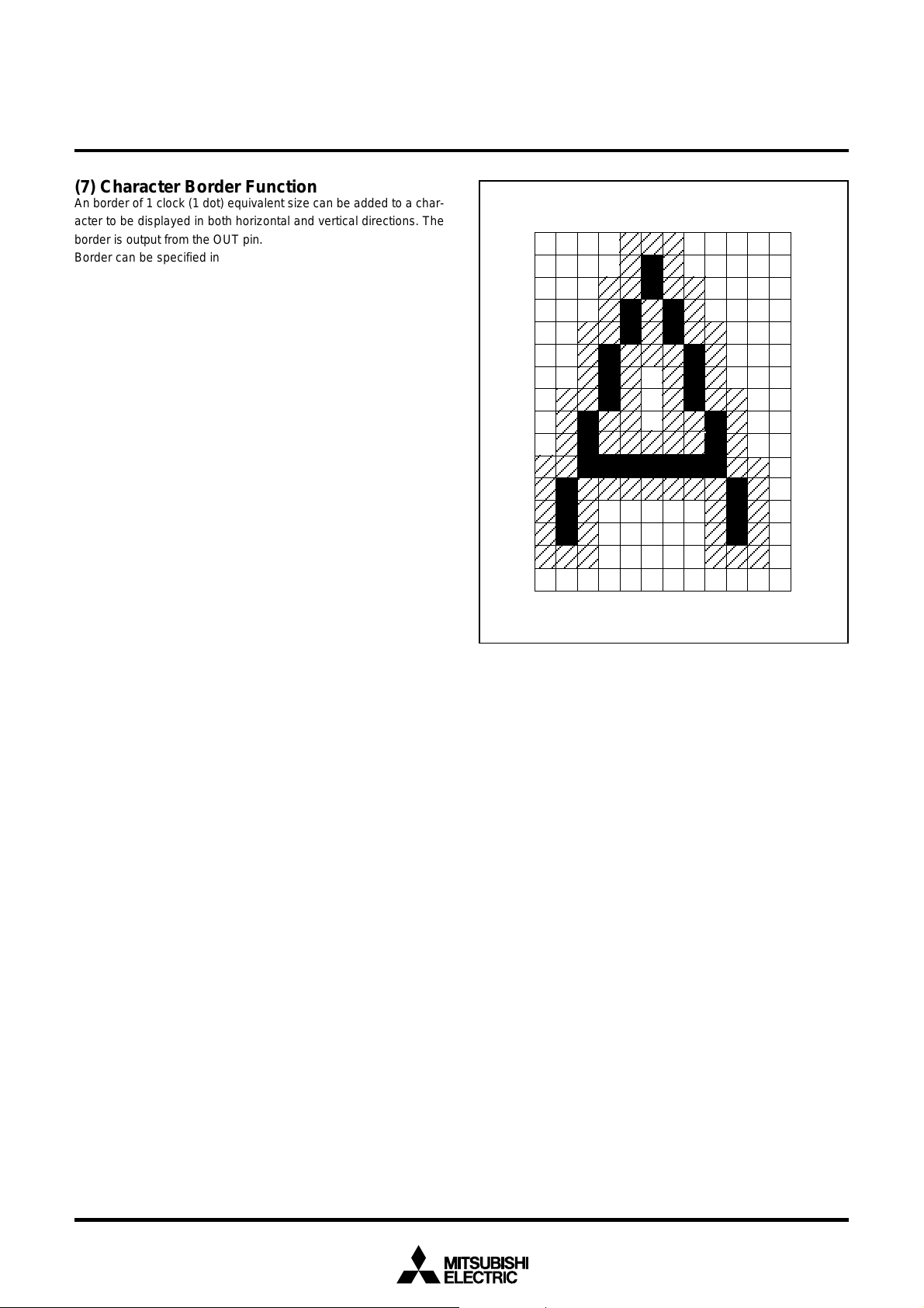
M37207MF-XXXSP/FP, M37207M8-XXXSP
SINGLE-CHIP 8-BIT CMOS MICROCOMPUTER for VOLTAGE SYNTHESIZER
(7) Character Border Function
An border of 1 clock (1 dot) equivalent size can be added to a character to be displayed in both horizontal and vertical directions. The
border is output from the OUT pin.
Border can be specified in units of block by using the border selection register (address 00E516). The setting of the border takes priority of the setting by bit 5 of the color register, however, the border of
the character to which a background color has been set cannot be
output. Figure 58 shows the border selection register. Table 12 shows
the relationship between the values set in the border selection register and the character border function.
MITSUBISHI MICROCOMPUTERS
M37207EFSP/FP
and ON-SCREEN DISPLAY CONTROLLER
Fig. 57. Example of Border
62
Page 63

Border Selection Register
b7 b6 b5 b4 b3 b2 b1 b0
Border selection register (MD) [Address 00E5
MITSUBISHI MICROCOMPUTERS
M37207MF-XXXSP/FP, M37207M8-XXXSP
M37207EFSP/FP
SINGLE-CHIP 8-BIT CMOS MICROCOMPUTER for VOLTAGE SYNTHESIZER
and ON-SCREEN DISPLAY CONTROLLER
16
]
B Name Functions
0 Block 1 OUT output
border selection bit (MD10)
1
Block 1 OUT output
switch bit (MD11)
2 Block 2 OUT output
border selection bit (MD20)
3
switch bit (MD21)
4 Block 3 OUT output
border selection bit (MD30)
5
switch bit (MD31)
6, 7
Nothing is assigned. These bits are write disable bits.
When these bits are read out, the values are “0.”
0 : Same output as character output
1 : Border output
0 : Border including character
1 : Border only
0 : Same output as character output
1 : Border output
0 : Border including character
1 : Border only
0 : Same output as character output
1 : Border output
0 : Border including character
1 : Border only
After reset
Indeterminate
Indeterminate
Indeterminate
Indeterminate
Indeterminate
Indeterminate
Fig. 58. Border Selection Register
Table 12. Relationship between Set Value in Border Selection Register and Character Border Function
Border Selection Register
MDn1
✕
MDn1
0
Functions
Ordinary
Example of Output
R, G, B, I output
OUT output
0
R
W
RW
RW
RW
RWBlock 2 OUT output
RW
RWBlock 3 OUT output
R—
0 Border including character output
1 Border only output
1
1
R, G, B, I output
OUT output
R, G, B, I output
OUT output
63
Page 64
M37207MF-XXXSP/FP, M37207M8-XXXSP
SINGLE-CHIP 8-BIT CMOS MICROCOMPUTER for VOLTAGE SYNTHESIZER
(8) Multiline Display
This microcomputer can ordinarily display 3 lines on the CRT screen
by displaying 3 blocks at different vertical positions. In addition, it can
display up to 16 lines by using CRT interrupts.
A CRT interrupt request occurs at the point at which display of each
block has been completed. In other words, when a scanning line
reaches the point of the display position (specified by the vertical
position registers) of a certain block, the character display of that
block starts, and an interrupt occurs at the point at which the scanning line exceeds the block.
Note: A CRT interrupt does not occur at the end of display when
the block is not displayed. In other words, if a block is set to
off display with the display control bit of the CRT control register 1 (address 00EA16), a CRT interrupt request does not
occur (refer to Figure 59).
MITSUBISHI MICROCOMPUTERS
M37207EFSP/FP
and ON-SCREEN DISPLAY CONTROLLER
Block 1 (on display)
Block 2 (on display)
Block 1' (on display)
Block 2' (on display)
On display (CRT interrupt request occurs at the end of block
display)
Block 1 (on display)
Block 2 (on display)
Block 1' (off display)
Block 2' (off display)
Off display (CRT interrupt request does not occur at the end
of block display)
“CRT interrupt request”
“CRT interrupt request”
“CRT interrupt request”
“CRT interrupt request”
“CRT interrupt request”
“CRT interrupt request”
No “CRT interrupt request”
No “CRT interrupt request”
Fig. 59. Timing of CRT Interrupt Request
64
Page 65

M37207MF-XXXSP/FP, M37207M8-XXXSP
SINGLE-CHIP 8-BIT CMOS MICROCOMPUTER for VOLTAGE SYNTHESIZER
The display block counter counts the number of times the display of
a block has been completed, and its contents are incremented by 1
each time the display of one block is completed.
To provide multi-line display, enable CRT interrupts by clearing the
interrupt disable flag to “0” and setting the CRT interrupt enable bit
(bit 4 of address 00FE16) to “1.” After that, process the following
sequence within the CRT interrupt processing routine:
ead the value of the display block counter.
The block for which display is terminated (i.e., the cause of CRT
interrupt generation) can be determined by the value read in .
Replace the display character data and vertical display position of
that block with the character data (contents of CRT display RAM)
and vertical display position (contents of vertical position register)
to be displayed next.
Figure 60 shows the structure of the display block counter.
MITSUBISHI MICROCOMPUTERS
M37207EFSP/FP
and ON-SCREEN DISPLAY CONTROLLER
Display Block Counter
b7 b6 b5 b4 b3 b2 b1 b0
Fig. 60. Display Counter
Display block counter (CBC) [Address 00EB
B Name Functions
0
Number of blocks which are being displayed or has
to
displayed
3
(Incremented each time a block is displayed)
Nothing is assigned. These bits are write disable bits.
to
When these bits are read out, the values are “0.”
7
Block 1
Block 2
Block 3
16
]
Count value
0
1
2
After reset
Indeterminate
Interrupt position
0
R
RW
R—4
W
Block 1’
Fig. 61. Timing of CRT Interrupt Request and Display Counter Value
3
4
65
Page 66
MITSUBISHI MICROCOMPUTERS
M37207MF-XXXSP/FP, M37207M8-XXXSP
M37207EFSP/FP
SINGLE-CHIP 8-BIT CMOS MICROCOMPUTER for VOLTAGE SYNTHESIZER
and ON-SCREEN DISPLAY CONTROLLER
(9) Scanning Line Double Count Mode
1 dot in a displayed character is normally shown with 1 scanning line.
In the scanning double count mode, 1 dot can be shown with 2 scanning lines. As a result, the displayed dot is extended 2 times the
normal size in the vertical direction only (that is to say, the height of a
character is extended twofold.)
In addition, because the scanning line count is doubled, the display
start position of a character becomes also twofold position in the
vertical direction.
In other words, the contents of the vertical position register is as follows:
• In ordinary mode
256 steps as values “0016” to “FF16”
(4 scanning lines per step)
• In scanning line double count mode
128 steps as values “0016” to “7F16”
(8 scanning lines per step)
Vertical position A
Scanning line 16 lines
If the contents of the vertical position register for a block are set in
the range of “8016” to “FF16” in the scanning line double count mode,
that block cannot be displayed (not output to the CRT screen). The
scanning line double count mode is specified by setting bit 6 of the
CRT control register 1 (address 00EA16) to “1.”
Since this function works in units of a screen, even if the mode is
changed during display of 1 screen, the mode before the change
remains until the display of the next screen.
Vertical position A ✕ 2
A ✕ 2
Scanning line 32 lines
(a) Display in the ordinary mode (b) Display in the scanning line double count mode
Fig. 62. Display in Ordinary Mode and in Scanning Line Double Count Mode
66
Page 67

M37207MF-XXXSP/FP, M37207M8-XXXSP
SINGLE-CHIP 8-BIT CMOS MICROCOMPUTER for VOLTAGE SYNTHESIZER
(10) Wipe Function
Wipe mode
This microcomputer allows the display area to be gradually expanded
or shrunk in the vertically direction in units of 1H (H: HSYNC signal).
There are 3 modes for this scroll method. Each mode has DOWN
and UP modes, providing a total of 6 modes.
Table 13 shows the contents of each wipe mode.
Table 13. Wipe Operation in Each Mode and Values of Wipe Mode Register
Mode Wipe Operation
MITSUBISHI MICROCOMPUTERS
M37207EFSP/FP
and ON-SCREEN DISPLAY CONTROLLER
Wipe Mode Register
Bit 2 Bit 1 Bit 0
DOWN
1
UP
DOWN
2
UP
DOWN
3
UP
Appear from
upper side
Erase from
lower side
Erase from
upper side
Appear from
lower side
Erase from
both upper and
lower sides
Appear to
both upper and
lower sides
AFBCDE
GLHIJK
MRNOPQ
SXTUVW
AFBCDE
GLHIJK
MRNOPQ
SXTUVW
AFBCDE
GLHIJK
MRNOPQ
SXTUVW
Down Up
ON
OFF
Down Up
OFF
ON
Down Up
OFF
ON
OFF
001
101
010
110
011
111
67
Page 68

MITSUBISHI MICROCOMPUTERS
M37207MF-XXXSP/FP, M37207M8-XXXSP
M37207EFSP/FP
SINGLE-CHIP 8-BIT CMOS MICROCOMPUTER for VOLTAGE SYNTHESIZER
and ON-SCREEN DISPLAY CONTROLLER
Wipe speed
The wipe speed is determined by the vertical synchronization (VSYNC)
signal. For the NTSC interlace method, assuming that
VSYNC = 16.7 ms, 262.5 HSYNC signals (per field)
we obtain the wipe speed as shown in Table 14.
Wipe resolution varies with each wipe mode. In mode 1 and mode 2,
one of 3 resolutions (1H, 2H, 4H) can be selected. In mode 3, wipe is
done in units of 4H only.
Wipe Mode Register
b7 b6 b5 b4 b3 b2 b1 b0
Wipe mode register (SL) [Address 00ED
B Name Functions
0, 1 Wipe mode selection bits
(SL0, SL1)
Direction mode selection
2
bits (SL2)
Wipe unit selection bits
3, 4
(SL3, SL4)
Stop mode selection bits
5, 6
(SL5, SL6)
Table 14. Wipe Speed
(NTSC interlace method, H = 262.5)
Wipe Resolution
1H Unit
2H Unit
4H Unit
Wipe Speed (entire screen)
16.7 (ms) ✕ 262.5 ÷ 1 4 (s)
16.7 (ms) ✕ 262.5 ÷ 2 2 (s)
16.7 (ms) ✕ 262.5 ÷ 4 1 (s)
Table 15. Wipe Mode and Wipe Resolution
Mode
Mode 1
Mode 2
Wipe Resolution
1H Unit
2H Unit
4H Unit
Mode 3
16
]
b1 b0
0 0 : Wipe is not available
0 1 : Mode 1
1 0 : Mode 2
1 1 : Mode 3
0: DOWN mode
1: UP mode
b4 b3
0 0 : 1H unit
0 1 : 2H unit
1 0 : 3H unit
1 1 : Do not set
b6 b5
0 0 : Stop at the 312nd H
0 1 : Stop at the 156th H
1 0 : Stop at the 256th H
1 1 : Stop at the 128th H
4H Unit
After reset
0
0
0
0
Wipe Speed
about 4 (s)
about 2 (s)
about 1 (s)
about 1 (s)
R
W
RW
RW
RW
RW
Fig. 63. Structure of Wipe Mode Register
68
7
Nothing is assigned. This bit is a write disable bit.
When this bit is read out, the value is indeterminate.
0
R—
Page 69

M37207MF-XXXSP/FP, M37207M8-XXXSP
SINGLE-CHIP 8-BIT CMOS MICROCOMPUTER for VOLTAGE SYNTHESIZER
(11) CRT Output Pin Control
The CRT output pins R, G, B, I and OUT can also function as ports
P52, P53, P54, P55 and P56. Set the corresponding bit of the port P5
control register (address 00CB16) to “0” to specify these pins as CRT
output pins, or set it to “1” to specify it as a general-purpose port P5
pins.
The input polarity of signals HSYNC and VSYNC and output polarity of
signals R, G, B, I and OUT can be specified with the bits of the CRT
port control register (address 00EC16). Set a bit to “0” to specify positive polarity; set it to “1” to specify negative polarity.
The CRT clock I/O pins OSC1, OSC2 are controlled with the port
control register (address 020616).
The CRT port control register is shown in Figure 64.
The port control register is shown in Figure 65.
CRT Port Control Register
b7 b6 b5 b4 b3 b2 b1 b0
CRT port control register (CRTP) [Address 00EC
MITSUBISHI MICROCOMPUTERS
M37207EFSP/FP
and ON-SCREEN DISPLAY CONTROLLER
16
]
Fig. 64. CRT Port Control Register
Port Control Register
b7 b6 b5 b4 b3 b2 b1 b0
B Name Functions
0H
SYNC
input polarity
switch bit (HSYC)
1
V
SYNC
input polarity
switch bit (VSYC)
2 R, G, B output polarity
switch bit (R/G/B)
3 I output polarity switch bit
(I)
4 OUT output polarity
switch bit (OUT)
5 R signal output switch bit
(R)
6 G signal output switch bit
(G)
7 B signal output switch bit
(B)
Port control register (P7D) [Address 0206
B Name Functions
0, 1 Port P7 data input bits
(P7D0, P7D1)
D-A/AD3 function selection
2
bit (P7D2)
0 : Positive polarity
1 : Negative polarity
0 : Positive polarity
1 : Negative polarity
0 : Positive polarity
1 : Negative polarity
0 : Positive polarity
1 : Negative polarity
0 : Positive polarity
1 : Negative polarity
0 : R signal output
1 : MUTE signal output
0 : G signal output
1 : MUTE signal output
0 : B signal output
1 : MUTE signal output
16
]
When only OP1 = “0” and
OP0 = ”1,” input data is
valid. (See note)
0: AD3
1: D-A
After reset
Indeterminate
0
0
0
0
0
0
0
0
After reset
0
R
RW
RW
RW
RW
RW
RW
RW
RW
W
R
W
RW
RW
Fig. 65. Port Control Register
Nothing is assigned. These bits are write disable bits.
3,
When these bits are read out, the values are indeterminate.
5 to 7
4P40/X
Note: OP is the CRT clock selection register.
CIN
, P41/X
function selection bit
(P7D4)
COUT
0 : P4
1 : X
CIN
0
, P4
, X
1
COUT
0
0
R—
RW
69
Page 70

M37207MF-XXXSP/FP, M37207M8-XXXSP
SINGLE-CHIP 8-BIT CMOS MICROCOMPUTER for VOLTAGE SYNTHESIZER
(12) Raster Coloring Function
An entire screen (raster) can be colored by switching each of the R,
G, and B pins to MUTE output. R, G, B are controlled with the CRT
port control register; I is controlled with the CRT control register 2;
OUT is controlled with the character size register. 15 raster colors
can be obtained.
If the OUT pin has been set to raster coloring output, a raster coloring signal is always output during 1 horizontal scanning period. This
setting is necessary for erasing a background TV image.
If the R, G, and B pins have been set to MUTE signal output, a raster
coloring signal is output in the part except a no-raster colored character (in Figure 66, a character “O”) during 1 horizontal scanning
period. This ensures that character colors do not mix with the raster
color. In this case, MUTE signal is output from the OUT pin.
An example in which a magenta character “I” and a red character “O”
are displayed with blue raster coloring is shown in Figure 66.
MITSUBISHI MICROCOMPUTERS
M37207EFSP/FP
and ON-SCREEN DISPLAY CONTROLLER
Fig. 66. Example of Raster Coloring
CRT Control Register 2
b7 b6 b5 b4 b3 b2 b1 b0
H
SYNC
R
B
OUT
A'A
Signals
across
A – A'
CRT control register 2 (CBR) [Address 0208
B Name Functions
0 I signal output switch bit
(CBR0)
0: I signal output
1: MUTE signal output
16
]
“RED”
“BLUE”
After reset
0
R
W
RW
Fig. 67. CRT Control Register 2
70
I/TIM1 function switch bit
1
(CBR1)
Nothing is assigned. These bits are write disable bits.
2
When these bits are read out, the values are indeterminate.
to
7
0: I output or MUTE output
1: 1/2 clock ouput of timer 1
0
0
RW
R—
Page 71

M37207MF-XXXSP/FP, M37207M8-XXXSP
SINGLE-CHIP 8-BIT CMOS MICROCOMPUTER for VOLTAGE SYNTHESIZER
(13) Clock for Display
As a clock for display to be used for CRT display, it is possible to
select one of the following 3 types.
Main clock supplied from the XIN pin
•
Clock from the LC or RC supplied from the pins OSC1 and OSC2.
•
Clock from the ceramic resonator or quartz-crystal oscillator sup-
•
plied from the pins OSC1 and OSC2.
This clock for display can be selected for each block by the CRT
clock selection register (address 020916).
When selecting the main clock, set the oscillation frequency to
8 MHz.
CRT Clock Selection Register
b7 b6 b5 b4 b3 b2 b1 b0
0
CRT clock selection register (OP) [Address 0209
MITSUBISHI MICROCOMPUTERS
M37207EFSP/FP
and ON-SCREEN DISPLAY CONTROLLER
16
]
B Name Functions After reset R
0, 1 CRT clock
2
to
6
7
Notes 1: It is necessary to connect other ceramic resonator or quartz-crystal oscillator across the pins X
Fig. 68. CRT Clock Selection Register
b1
b0
selection bits
(OP0, OP1)
Nothing is assigned. These bits are write disable bits.
When these bits are read out, the values are “0.”
Fix this bits to “0.”
2: CC6 is the scnanning line double count mode flag.
The clock for display is supplied by connecting RC
10
or LC across the pins OSC1 and OSC2.
0
1
Since the main clock is used as the clock for
display, the oscillation frequency is limited.
Because of this, the character size in width
(horizontal) direction is also limited. In this
case, pins OSC1 and OSC2 are also used
as input ports P7
Do not set.
0
1
11
The clock for display is supplied by connecting the
following across the pins OSC1 and OSC2.
•
a ceramic resonator only for CRT display and a feedback resistor
•
a quartz-crystal oscillator only for CRT display and a feedback
resistor (See note)
Functions
0
and P71 respectively.
CRT oscillation
frequency
IN
)
= f(X
CC6
CC6 =
“0” or “1”
CC6 = “0”
—
CC6 = “0”
RW
0
0
R—
0
RW
IN and XOUT.
W
71
Page 72

MITSUBISHI MICROCOMPUTERS
M37207MF-XXXSP/FP, M37207M8-XXXSP
M37207EFSP/FP
SINGLE-CHIP 8-BIT CMOS MICROCOMPUTER for VOLTAGE SYNTHESIZER
and ON-SCREEN DISPLAY CONTROLLER
INTERRUPT INTERVAL DETERMINATION FUNCTION
This microcomputer incorporates an interrupt interval determination
circuit. This interrupt interval determination circuit has an 8-bit binary
up counter as shown in Figure 69. Using this counter, it determines
an interval on the INT1 or INT2 (refer to Figure 72).
The following describes how the interrupt interval is determined.
1. The interrupt input to be determined (INT1 input or INT2 input) is
selected by using bit 2 in the interrupt interval determination control register (address 00D816). When this bit is cleared to “0,” the
INT1 input is selected ; when the bit is set to “1,” the INT2 input is
selected.
2. When the INT1 input is to be determined, the polarity is selected
by using bit 3 of the interrupt interval determination control
register ; when the INT2 input is to be determined, the polarity is
selected by using bit 4 of the interrupt interval determination
control register.
When the relevant bit is cleared to “0,” determination is made of
the interval of a positive polarity (rising transition) ; when the bit is
set to “1,” determination is made of the interval of a negative polarity (falling transition).
3. The reference clock is selected by using bit 1 of the interrupt interval determination control register. When the bit is cleared to “0,” a
32 ms clock is selected ; when the bit is set to “1,” a 16 ms clock is
selected (based on an oscillation frequency of 8MHz in either
case).
4. Simultaneously when the input pulse of the specified polarity
(rising or falling transition) occurs on the INT1 pin (or INT2 pin),
the 8-bit binary up counter starts counting up with the selected
reference clock (32 ms or 16 ms).
5. Simultaneously with the next input pulse, the value of the 8-bit
binary up counter is loaded into the interrupt interval determination register (address 00D716) and the counter is immediately reset (“0016”). The reference clock is input in succession even after
the counter is reset, and the counter restarts counting up from
“0016.”
6. When count value “FE16” is reached, the 8-bit binary up counter
stops counting. Then, simultaneously when the next reference
clock is input, the counter sets value “FF16” to the interrupt interval determination register. The reference clock is generated by
setting bit 0 of PWM mode register 1 to “0.”
16µs
32µs
RE1
INT2 (Note)
INT1 (Note)
RE2
Selection gate :
RE : Interrupt interval determination control register
Note: The pulse width of external interrupt INT1 and INT2 needs 5 or more machine cycles.
Fig. 69. Block Diagram of Interrupt Interval Determination Circuit
Control
circuit
Connected to
black colored
side at rest.
RE0
Interrupt interval determination register (8)
8-bit binary up counter (8)
8
(Address 00D716)
8
Data bus
72
Page 73

M37207MF-XXXSP/FP, M37207M8-XXXSP
SINGLE-CHIP 8-BIT CMOS MICROCOMPUTER for VOLTAGE SYNTHESIZER
Interrupt Interval Determination Control Register
b7 b6 b5 b4 b3 b2 b1 b0
interrupt interval determination control register (RE) [Address 00D8
MITSUBISHI MICROCOMPUTERS
M37207EFSP/FP
and ON-SCREEN DISPLAY CONTROLLER
16
]
B Name Functions
0 Interrupt interval
determination circuit
operation control bit (RE0)
1 Reference clock selection
bit (RE1)
2 External interrupt input
pin selection bit (RE2)
3 INT1 pin input polarity
switch bit (RE3)
4 INT2 pin input polarity
switch bit (RE4)
5
Nothing is assigned. These bits are write disable bits.
to
When these bits are read out, the values are “0.”
7
Fig. 70. Interrupt Interval Determination Control Register
INT1 or INT2 input
Count interval
0 : Stopped
1 : Operating
0 : 16 µs
1 : 32 µs
IN
) = 8 MHz)
(at f(X
0 : INT1 input
1 : INT2 input
0 : Positive polarity input
1 : Negative polarity input
0 : Positive polarity input
1 : Negative polarity input
After reset
0
0
0
0
0
0
R
W
RW
RW
RW
RW
RW
R—
Fig. 71. Measuring Interval
73
Page 74

M37207MF-XXXSP/FP, M37207M8-XXXSP
SINGLE-CHIP 8-BIT CMOS MICROCOMPUTER for VOLTAGE SYNTHESIZER
ROM CORRECTION FUNCTION
This can correct program data in ROM. Up to 2 addresses (2 blocks)
can be corrected, a program for correction is stored in the ROM correction memory in RAM. The ROM memory for correction is 32 bytes
✕ 2 blocks.
Block 1 : addresses 02C016 to 02DF16
Block 2 : addresses 02E016 to 02FF16
Set the address of the ROM data to be corrected into the ROM correction address register. When the value of the counter matches the
ROM data address in the ROM correction address, the main program branches to the correction program stored in the ROM memory
for correction. To return from the correction program to the main program, the op code and operand of the JMP instruction (total of 3
bytes) are necessary at the end of the correction program. When the
blocks 1 and 2 are used in series, the above instruction is not needed
at the end of the block 1.
The ROM correction function is controlled by the ROM correction
enable register.
Notes 1 : Specify the first address (op code address) of each
instruction as the ROM correction address.
2 : Use the JMP instruction (total of 3 bytes) to return from
the correction program to the main program.
3 : Do not set the same ROM correction address to the blocks
1 and 2.
MITSUBISHI MICROCOMPUTERS
M37207EFSP/FP
and ON-SCREEN DISPLAY CONTROLLER
ROM correction address 1 (high-order)
ROM correction address 1 (low-order)
ROM correction address 2 (high-order)
ROM correction address 2 (low-order)
Fig. 72. ROM Correction Address Registers
0217
0218
0219
021A
16
16
16
16
ROM Correction Enable Register
b7 b6 b5 b4 b3 b2 b1 b0
00
Fig. 73. ROM Correction Enable Register
ROM correction enable register (RCR) [Address 021B16]
B
0 Block 1 enable bit (RC0)
1 Block 2 enable bit (RC1) 0: Disabled
2, 3
4
to
7
Name Functions
0: Disabled
1: Enabled
1: Enabled
Fix these bits to“0.”
Nothing is assigned. These bits are write disable bits. When
these bits are read out, the values are “0.”
After reset
0
0
0
0
RW
RW
RW
RW
R—
74
Page 75
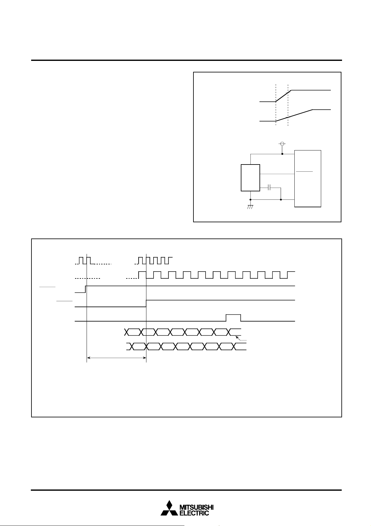
MITSUBISHI MICROCOMPUTERS
M37207MF-XXXSP/FP, M37207M8-XXXSP
M37207EFSP/FP
SINGLE-CHIP 8-BIT CMOS MICROCOMPUTER for VOLTAGE SYNTHESIZER
and ON-SCREEN DISPLAY CONTROLLER
RESET CIRCUIT
When the oscillation of a quartz-crystal oscillator or a ceramic resonator is stable and the power source voltage is 5 V ± 10 %, hold the
______
RESET pin at LOW for 2 µs or more, then return is to HIGH. Then, as
shown in Figure 75, reset is released and the program starts from
the address formed by using the content of address FFFF16 as the
high-order address and the content of the address FFFE16 as the
low-order address. The internal state of microcomputer at reset are
shown in Figure 75.
An example of the reset circuit is shown in Figure 74.
The reset input voltage must be kept 0.6 V or less until the power
source voltage surpasses 4.5 V.
Poweron
Power source voltage 0 V
Reset input voltage 0 V
1
5
M51953AL
4
0.1µF
3
Fig. 74. Example of Reset Circuit
4.5 V
0.6 V
Vcc
RESET
Vss
Microcomputer
XIN
φ
RESET
Internal RESET
SYNC
Address
Data
Fig. 75. Reset Sequence
32768 count of XIN
clock cycle (Note 3)
01, S-1
? ?
? ? ? ? ?
01, S
Notes 1 :
01, S-2
FFFE FFFF
ADL ADH
f(XIN) and f(φ) are in the relation : f(XIN) = 2·f (φ).
:
2 A question mark (?) indicates an undefined state that
depends on the previous state.
:
3
Immediately after a reset, timer 3 and timer 4 are
connected by hardware. At this time, “FF
in timer 3 and “07
with f(X
overflow signal.
ADH,
ADL
Reset address from the vector table
IN)/16, and reset state is released by the timer 4
16” is set to timer 4. Timer 3 counts down
16” is set
75
Page 76

MITSUBISHI MICROCOMPUTERS
M37207MF-XXXSP/FP, M37207M8-XXXSP
M37207EFSP/FP
SINGLE-CHIP 8-BIT CMOS MICROCOMPUTER for VOLTAGE SYNTHESIZER
and ON-SCREEN DISPLAY CONTROLLER
CLOCK GENERATING CIRCUIT
This microcomputer has 2 built-in oscillation circuits. An oscillation
circuit can be formed by connecting a resonator between X
OUT (XCIN and XCOUT). Use the circuit constants in accordance with
X
IN and
the resonator manufacturer’s recommended values. No external resistor is needed between X
IN and XOUT since a feed-back resistor
exists on-chip. However, an external feed-back resistor is needed
between X
CIN and XCOUT. When using XCIN-XCOUT as sub-clock,
clear bits 7 and 6 of the mixing control register to “0.” To supply a
clock signal externally, input it to the X
OUT (XCOUT) pin open. When not using XCIN clock, connect the
X
CIN to VSS and make the XCOUT pin open.
X
IN (XCIN) pin and make the
After reset has completed, the internal clock φ is half the frequency of
IN. Immediately after poweron, both the XIN and XCIN clock start
X
oscillating. To set the internal clock φ to low-speed operation mode,
set bit 7 of the CPU mode register (address 00FB
16) to “1.”
Oscillation Control
(1) Stop mode
The built-in clock generating circuit is shown in Figure 78. When the
STP instruction is executed, the internal clock φ stops at HIGH. At
keeps its
16”
the same time, timers 3 and 4 are connected by hardware and “FF
is set in timer 3 and “07
CIN)/16 as the timer 3 count source (set bit 0 of the timer mode
f(X
16” is set in the timer 4. Select f(XIN)/16 or
register 2 to “0” before the execution of the STP instruction). Moreover, set the timer 3 and timer 4 interrupt enable bits to disabled (“0”)
before execution of the STP instruction. The oscillator restarts when
external interrupt is accepted. However, the internal clock φ
HIGH until timer 4 overflows, allowing time for oscillation stabilization
when a ceramic resonator or a quartz-crystal oscillator is used.
(3) Low-Speed Mode
If the internal clock is generated from the sub-clock (XCIN), a low
power consumption operation can be realized by stopping only the
main clock X
mode register (00FB
the program must allow enough time to for oscillation to stabilize.
Note that in low-power-consumption mode the X
can be reduced, allowing even lower power consumption (20µA with
CIN) = 32kHz). To reduce the XCIN-XCOUT drivability, clear bit 5
f (X
(CM
set to “1” and strong drivability is selected to help the oscillation to
start. When an STP instruction is executed, set this bit to “1” by software before executing.
Fig. 76. Ceramic Resonator Circuit Example
IN. To stop the main clock, set bit 6 (CM6) of the CPU
16) to “1.” When the main clock XIN is restarted,
CIN-XCOUT drivability
5) of the CPU mode register (00FB16) to “0.” At reset, this bit is
Microcomputer
X
CIN
X
26 25 30 31
COUT
R
f
C
CIN
X
IN
X
OUT
R
d
C
COUT
C
IN
C
OUT
(2) Wait mode
When the WIT instruction is executed, the internal clock φ stops in
the “H” level but the oscillator continues running. This wait state is
released at reset or when an interrupt is accepted (Note). Since the
oscillator does not stop, the next instruction can be executed at once.
Note: In the wait mode, the following interrupts are invalid.
SYNC interrupt
(1) V
(2) CRT interrupt
IN)/4096 interrupt
(3) f(X
(4) Timer 1 and 2 interrupts using TIM2 pin input as count
source
(5) Timer 1 interrupt using f(X
count source
(6) Timer 3 interrupt using TIM3 pin input as count source
2
(7) Multi-master I
C-BUS interface interrupt
(8) Timer 4 interrupt using f(X
IN)/4096 or f(XCIN)/4096 as
IN)/2 or f(XCIN)/2 as count souce
Microcomputer
X
CIN
X
COUTXINXOUT
Open Open
External oscillation
circuit or external
External oscillation
circuit
pulse
Vcc
Vss
Vcc
Vss
Fig. 77. External Clock Input Circuit Example
76
Page 77
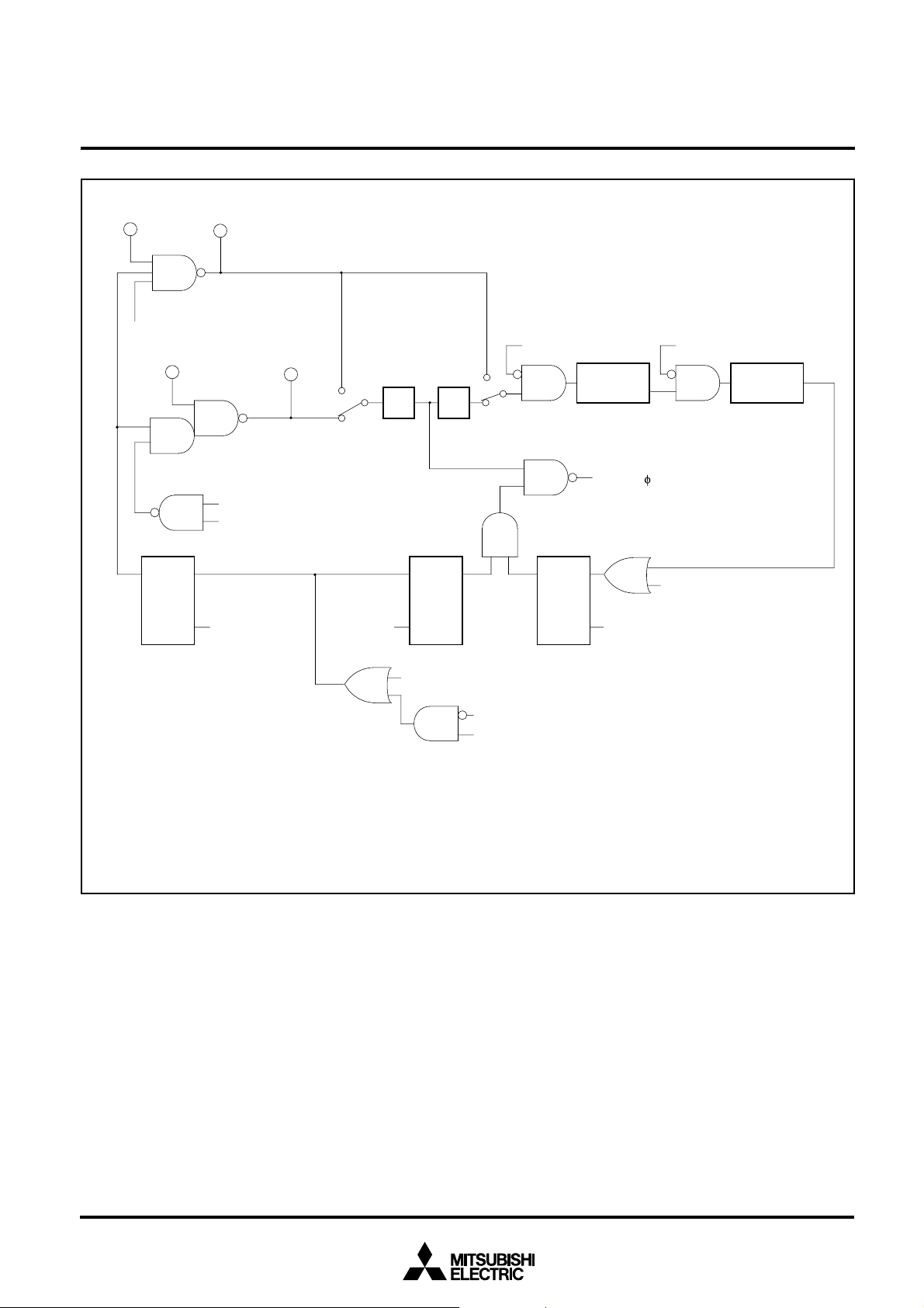
X
CIN
P40/X
CIN
function selection bit
(Notes 1, 4)
X
IN
X
COUT
, P41/X
COUT
Internal system clock
selection bit (Notes 1, 3)
Main clock (X
Internal system clock
selection bit (Notes 1, 3)
X
OUT
“1”
“0”
IN–XOUT
) stop bit (Notes 1, 3)
MITSUBISHI MICROCOMPUTERS
M37207MF-XXXSP/FP, M37207M8-XXXSP
M37207EFSP/FP
SINGLE-CHIP 8-BIT CMOS MICROCOMPUTER for VOLTAGE SYNTHESIZER
and ON-SCREEN DISPLAY CONTROLLER
Timer 4 count
stop bit (Notes 1, 2)
1/2
Timer 3 count
stop bit (Notes 1, 2)
“1”
1/8
“0”
Timer 3
count source selection bit (Notes 1,2)
Timer 3 Timer 4
Timing
(Internal clock)
SQ
R
STP instruction
Notes 1:
Fig. 78. Clock Generating Circuit Block Diagram
WIT
instruction
The value at reset is “0.”
2:
Refer to the structure of timer mode register 2.
3:
Refer to the structure of CPU mode register (next page).
4:
Refer to the structure of port control register.
S
R
Reset
Q
Interrupt disable flag I
Interrupt request
Q
S
STP instruction
R
Reset
77
Page 78
MITSUBISHI MICROCOMPUTERS
M37207MF-XXXSP/FP, M37207M8-XXXSP
M37207EFSP/FP
SINGLE-CHIP 8-BIT CMOS MICROCOMPUTER for VOLTAGE SYNTHESIZER
and ON-SCREEN DISPLAY CONTROLLER
8MHz oscillating
32kHz oscillating
φ is stopped (HIGH)
Timer operating
8MHz oscillating
32kHz oscillating
φ is stopped (HIGH)
Timer operating
8MHz oscillating
32kHz oscillating
φ is stopped (HIGH)
Timer operating
(Note 3)
WIT instruction
Interrupt
External INT,
timer interrupt,
or SI/O interrupt
WIT instruction
Interrupt
External INT,
timer interrupt,
or SI/O interrupt
WIT instruction
Interrupt
8MHz oscillating
32kHz oscillating
XC = 1
8MHz oscillating
32kHz oscillating
CM7 = 1
8MHz oscillating
32kHz oscillating
Reset
f(φ) = 4MHz
f(φ) = 4MHz
f(φ) = 16kHz
High-speed operation
start mode
STP instruction
Interrupt (Note 1)
External INT,
XC = 0
CM7 = 0
or SI/O interrupt
STP instruction
Interrupt (Note 1)
External INT
STP instruction
Interrupt (Note 2)
8MHz stopped
32kHz stopped
is stopped (HIGH)
φ
8MHz stopped
32kHz stopped
is stopped (HIGH)
φ
8MHz stopped
32kHz stopped
is stopped (HIGH)
φ
8MHz stopped
32kHz oscillating
φ is stopped (HIGH)
Timer operating
(Note 3)
The example assumes that 8 MHz is being applied to the XIN pin and 32 kHz to the X
Notes 1: When the STP state is ended, a delay of approximately 8ms is automatically generated by timer 3 and timer 4.
2: The delay after the STP state ends is approximately 2s.
3: When the internal clock φ divided by 8 is used as the timer count source, the frequency of the count source is 2kHz.
Fig. 79. State Transitions of System Clock
WIT instruction
Interrupt
Port control register
(Address : 0206
XC: P40/X
selection bit
0 : P4
1 : X
CIN
CM6 = 1
, P41/X
0
, P4
CIN
, X
8MHz stopped
32kHz oscillating
f(φ) = 16kHz
16
)
COUT
function
1
COUT
CM6 = 0
The program must
allow time for 8MHz
oscillation to stabilize
STP instruction
Interrupt (Note 2)
CM6 : Main clock (XIN–X
0 : Oscillating
1 : Stopped
CM7 : Internal system clock selection bit
0 : X
1 : X
IN–XOUT
CIN–XCOUT
CIN
pin. The φ indicates the internal clock.
8MHz stopped
32kHz stopped
= stopped (HIGH)
φ
CPU mode register
(Address : 00FB
OUT
selected (high-speed mode)
selected (low-speed mode)
) stop bit
16
)
78
Page 79

M37207MF-XXXSP/FP, M37207M8-XXXSP
SINGLE-CHIP 8-BIT CMOS MICROCOMPUTER for VOLTAGE SYNTHESIZER
DISPLAY OSCILLATION CIRCUIT
The CRT display clock oscillation circuit has a built-in clock oscillation circuits, so that a clock for CRT display can be obtained simply
by connecting an LC, an RC, a quartz-crystal oscillator or a ceramic
resonator across the pins OSC1 and OSC2. Which of the sub-clock
or the display oscillation circuit is selected by setting bits 0 and 1 of
the CRT clock selection register (address 020916).
OSC2OSC1
L
C1
Fig. 80. Display Oscillation Circuit
AUTO-CLEAR CIRCUIT
When a power source is supplied, the auto-clear function will operate by connecting the following circuit to the RESET pin.
C2
______
MITSUBISHI MICROCOMPUTERS
M37207EFSP/FP
and ON-SCREEN DISPLAY CONTROLLER
ADDRESSING MODE
The memory access is reinforced with 17 kinds of addressing modes.
Refer to SERIES 740 <Software> User’s Manual for details.
MACHINE INSTRUCTIONS
There are 71 machine instructions. Refer to SERIES 740 <Soft- ware>
User’s Manual for details.
PROGRAMMING NOTES
(1) The divide ratio of the timer is 1/(n+1).
(2) Even though the BBC and BBS instructions are executed imme-
diately after the interrupt request bits are modified (by the program), those instructions are only valid for the contents before
the modification. At least one instruction cycle is needed (such as
an NOP) between the modification of the interrupt request bits
and the execution of the BBC and BBS instructions.
(3) After the ADC and SBC instructions are executed (in the decimal
mode), one instruction cycle (such as an NOP) is needed before
the SEC, CLC, or CLD instruction is executed.
(4) An NOP instruction is needed immediately after the execution of
a PLP instruction.
(5) In order to avoid noise and latch-up, connect a bypass capacitor
(≈ 0.1 µF) directly between the VCC pin–VSS pin and the VCC pin–
CNVSS pin, using a thick wire.
Circuit example 1
RESET
Circuit example 2
RESET
Note : Make the level change from LOW to HIGH at the point at
which the power source voltage exceeds the specified
voltage.
Fig. 81. Auto-clear Circuit Example
Vcc
Vss
Vcc
Vss
79
Page 80

MITSUBISHI MICROCOMPUTERS
M37207MF-XXXSP/FP, M37207M8-XXXSP
M37207EFSP/FP
SINGLE-CHIP 8-BIT CMOS MICROCOMPUTER for VOLTAGE SYNTHESIZER
and ON-SCREEN DISPLAY CONTROLLER
DATA REQUIRED FOR MASK ORDERS
The following are necessary when ordering a mask ROM production:
(1) Mask ROM Order Confirmation Form
(2) Mark Specification Form
(3) Data to be written to ROM, in EPROM form (32-pin DIP type
27C101, three identical copies)
PROM Programming Method
The built-in PROM of the One Time PROM version (blank) and the
built-in EPROM version can be read or programmed with a generalpurpose PROM programmer using a special programming adapter.
Product
M37207EFSP
M37207EFFP
The PROM of the One Time PROM version (blank) is not tested or
screened in the assembly process nor any following processes. To
ensure proper operation after programming, the procedure shown in
Figure 82 is recommended to verify programming.
Screening (Caution)
(150°C for 40 hours)
Name of Programming Adapter
PCA4762
PCA7417
Programming with
PROM programmer
Verification with
PROM programmer
Functional check in target device
Caution : The screening temperature is far higher
than the storage temperature. Never
expose to 150°C exceeding 100 hours.
Fig. 82. Programming and Testing of One Time PROM Version
80
Page 81

ABSOLUTE MAXIMUM RATINGS
Symbol
VCC
VI
VI
VO
VO
IOH
IOL1
IOL2
IOL3
IOL4
Pd
Topr
Tstg
Power source voltage VCC
Input voltage CNVSS
Input voltage P00–P07, P10–P17, P20–P27,
Output voltage P00–P07, P10–P17, P20–P27,
Output voltage P46, P47, P60–P67
Circuit current R, G, B, I, OUT, P00–P07,
Circuit current R, G, B, I, OUT, P00–P07,
Circuit current P46, P47, P60–P67
Circuit current P24–P27
Circuit current P40–P45
Power dissipation
Operating temperature
Storage temperature
Parameter
P30–P36, P40–P47, P60–P67,
P70, P71,OSC1, XIN, HSYNC,
VSYNC, RESET, XCIN,
AD1–AD8
P30–P36, P40–P45, R, G, B, I,
OUT, D-A, XOUT, XCOUT,
OSC2
P10–P17, P20–P27, P30, P31,
D-A
P10–P17, P20–P23,P30–P36,
D-A
MITSUBISHI MICROCOMPUTERS
M37207MF-XXXSP/FP, M37207M8-XXXSP
M37207EFSP/FP
SINGLE-CHIP 8-BIT CMOS MICROCOMPUTER for VOLTAGE SYNTHESIZER
and ON-SCREEN DISPLAY CONTROLLER
Conditions
All voltages are based
on VSS.
Output transistors are
cut off.
______
Ta = 25 °C
Ratings
–0.3 to 6
–0.3 to 6
–0.3 to VCC + 0.3
–0.3 to VCC + 0.3
–0.3 to 13
0 to 1 (Note 1)
0 to 2 (Note 2)
0 to 1 (Note 2)
0 to 10 (Note 3)
0 to 6 (Note 2)
550
–10 to 70
–40 to 125
Unit
V
V
V
V
V
mA
mA
mA
mA
mA
mW
°C
°C
RECOMMENDED OPERATING CONDITIONS (Ta = –10 °C to 70 °C, VCC = 5 V ± 10 %, unless otherwise noted)
29
Limits
Typ.
5.0
0
0
0
0
8.0
32
Max.
5.5
0
VCC
VCC
0.4 VCC
0.3 VCC
0.2 VCC
10
8.1
35
13
100
400
Symbol Parameter
VCC
VSS
VIH1
VIH2
VIL1
VIL2
VIL3
IOH
IOL1
IOL2
IOL3
IOL4
f(XIN)
f(XCIN)
fOSC
fhs1
fhs2
fhs3
Power source voltage (Note 4), During CPU, CRT operation
Power source voltage
HIGH input voltage P00–P07, P10–P17, P20–P27, P30–P36,
HIGH input voltage SDA3, SCL3, S DA2, SCL2, SDA1, SCL1
LOW input voltage P00–P07, P10–P17, P20–P27, P30, P31,
LOW input voltage SDA3, SCL3, SDA2, SCL2, SDA1, SCL1
LOW input voltage
HIGH average output current (Note 1)
LOW average output current (Note 2)
LOW average output current (Note 2)
LOW average output current (Note 3)
LOW average output current (Note 2)
Oscillation frequency (for CPU operation) (Note 5) XIN
Oscillation frequency (for sub-clock operation) (Note 7)XCIN
Oscillation frequency (for CRT display) (Note 6) OSC1
Input frequency TIM2, TIM3, INT1, INT2
Input frequency SCLK1, SCLK2
Input frequency SCL1, SCL2, SCL3
P60–P67, P70, P71, HSYNC, VSYNC,
______
RESET, XIN, XCIN, OSC1,
P40–P47 (including when using serial I/O)
(When using I2C-BUS)
P35, P40–P47, P70, P71
(When using I2C-BUS)
HSYNC, VSYNC, RESET, P32–P34, P36,
P41, P42, P44–P46, XIN, XCIN, OSC1
When using serial I/O; SOUT2, SCLK2, SIN2,
SOUT1, SCLK1, SIN1
R, G, B, I, OUT, D-A, P00–P07, P10–P17,
P20–P27, P30, P31
R, G, B, I, OUT, D-A, P00–P07, P10–P17,
P20–P23, P30–P36
P46, P47, P60–P67
P24–P27
P40–P45
Min.
4.5
0.8VCC
0.7VCC
______
7.9
6.0
Unit
V
V
0
V
V
V
V
V
mA
1
mA
2
mA
1
mA
mA
6
MHz
kHz
MHz
kHz
MHz
1
kHz
81
Page 82

MITSUBISHI MICROCOMPUTERS
M37207MF-XXXSP/FP, M37207M8-XXXSP
M37207EFSP/FP
SINGLE-CHIP 8-BIT CMOS MICROCOMPUTER for VOLTAGE SYNTHESIZER
and ON-SCREEN DISPLAY CONTROLLER
ELECTRIC CHARACTERISTICS (VCC = 5 V ± 10 %, VSS = 0 V, f(XIN) = 8 MHz, Ta = –10 °C to 70 °C, unless otherwise noted)
Symbol
ICC
Power source current
Parameter
System operation
Test conditions
VCC = 5.5 V,
f(XIN) = 8 MHz
Min.
CRT OFF
CRT ON
Limits
Typ.
15
30
Max.
30
45
Unit
mA
VOH
VOL
VT+–VT–
IIZH
IIZL
IOZH
RBS
Wait mode
Stop mode
HIGH output voltage R, G, B, I, OUT, P00–P07,
LOW output voltage R, G, B, I, OUT, P00–P07,
LOW output voltage P46, P47, P60–P67
LOW output voltage P24–P27
LOW output voltage P40–P45
Hysteresis
Hysteresis (Note 8) HSYNC, VSYNC, P32, P33, P34,
HIGH input leak current
LOW input leak current
HIGH output leak current
I2C-BUS·BUS switch connection resistor
(between SCL1 and SCL2, SDA1 and SDA2)
P10–P17, P20–P27, D-A, P30,
P31
P10–P17, P20–P23, P30–P36,
D-A
______
RESET
P36, P40–P46,
______
RESET, P00–P07, P10–P17,
P20–P27, P30–P36, P40–P47,
AD1–AD8
______
RESET, P00–P07, P10–P17,
P20–P27, P30–P36, P40–P46,
P60–P67, AD1–AD8
P46, P47, P60–P67
VCC = 5.5 V, f(XIN) = 0,
f(XCIN) = 32kHz,
CRT OFF, Low-power
dissipation mode set
(CM5 = “0,” CM6 = “1”)
VCC = 5.5 V, f(XIN) = 8 MHz
VCC = 5.5 V, f(XIN) = 0,
f(XCIN) = 32kHz,
Low-power dissipation
mode set (CM5 = “0,” CM6 =
“1”)
VCC = 5.5 V, f(XIN) = 0,
f(XCIN) = 0
VCC = 4.5 V
IOH = –0.5 mA
VCC = 4.5 V
IOL = 0.5 mA
VCC = 4.5 V
IOL = 0.5 mA
VCC = 4.5 V
IOL = 10.0 mA
VCC = 4.5 V IOL = 3 mA
IOL = 6 mA
VCC = 5.0 V
VCC = 5.0 V
VCC = 5.5 V
VI = 5.5 V
VCC = 5.5 V
VI = 0 V
VCC = 5.5 V
VO = 12 V
VCC = 4.5 V
2.4
100
2
60
1
0.5
0.5
200
4
100
10
0.4
0.4
3.0
0.4
0.6
0.7
1.3
5
5
10
130
µA
mA
µA
V
V
V
µA
µA
µA
Ω
Notes 1: The total current that flows out of the IC must be 20 mA or less.
2: The total input current to IC (IOL1 + IOL2 + IOL4) must be 30 mA or less.
3: The total average input current for ports P24–P27 to IC must be 20 mA or less.
4: Connect 0.022 m F or more capacitor externally between the power source pins VCC–VSS so as to reduce power source noise.
Also connect 0.068 m F or more capacitor externally between the pins VCC–CNVSS.
5: Use a quartz-crystal oscillator or a ceramic resonator for the CPU oscillation circuit.
6: Use a RC or an LC for the CRT oscillation circuit.
7: When using the sub-clock, set fCLK < fCPU/3.
8: P32–P34 ,P36 have the hysteresis when these pins are used as interrupt input pins or timer input pins. P40–P46 have the hysteresis
when these pins are used as serial I/O pins.
82
Page 83
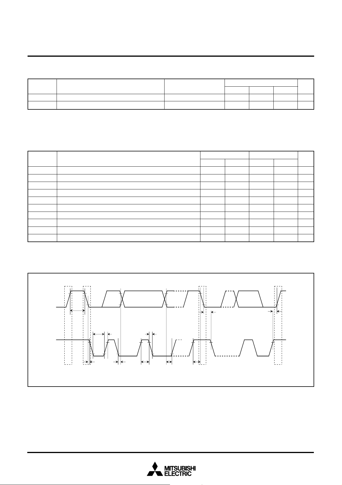
MITSUBISHI MICROCOMPUTERS
M37207MF-XXXSP/FP, M37207M8-XXXSP
SINGLE-CHIP 8-BIT CMOS MICROCOMPUTER for VOLTAGE SYNTHESIZER
and ON-SCREEN DISPLAY CONTROLLER
A-D COMPARATOR CHARACTERISTICS
(VCC = 5 V ± 10 %, VSS = 0 V, f(XIN) = 8 MHz, Ta = –10 °C to 70 °C, unless otherwise noted)
Symbol
—
— ±1
Note: When Vcc = 5 V, 1 LSB = 5/64 V.
Resolution
Absolute accuracy
MULTI-MASTER I2C-BUS BUS LINE CHARACTERISTICS
Symbol
tBUF
tHD:STA
tLOW
tR
tHD:DAT
tHIGH
tF
tSU:DAT
tSU:STA
tSU:STO
Note: Cb = total capacitance of 1 bus line
Bus free time
Hold time for START condition
“L” period of SCL clock
Rising time of both SCL and SDA signals
Data hold time
“H” period of SCL clock
Falling time of both SCL and SDA signals
Data set-up time
Set-up time for repeated START condition
Set-up time for STOP condition
Parameter
Parameter
Min.
0
Standard clock mode High-speed clock mode
Min.
4.7
4.0
4.7
0
4.0
250
4.7
4.0
Max.
1000
300
M37207EFSP/FP
Limits
Typ.
Min.
1.3
0.6
1.3
20+0.1Cb
0
0.6
20+0.1Cb
100
0.6
0.6
Max.
±2
Max.
300
0.9
300
UnitTest conditions
6
bits
LSB
Unit
µs
µs
µs
ns
µs
µs
ns
ns
µs
µs
SDA
t
BUF
t
LOW
P
SCL
Fig. 83. Definition diagram of timing on multi-master I2C-BUS
S
tHD:
STA
t
R
tHD:
DAT
t
HIGH
t
tSU:
tHD:
STA
F
Sr
S
tSU:
DAT
tSU:
STA
: Start condition
Sr
: Restart condition
P
: Stop condition
STO
P
83
Page 84

PACKAGE OUTLINE
64P4B
MITSUBISHI MICROCOMPUTERS
M37207MF-XXXSP/FP, M37207M8-XXXSP
M37207EFSP/FP
SINGLE-CHIP 8-BIT CMOS MICROCOMPUTER for VOLTAGE SYNTHESIZER
and ON-SCREEN DISPLAY CONTROLLER
80P6N–A
84
Page 85

GZZ–SH08–83B < 48B0 >
MITSUBISHI MICROCOMPUTERS
M37207MF-XXXSP/FP, M37207M8-XXXSP
M37207EFSP/FP
SINGLE-CHIP 8-BIT CMOS MICROCOMPUTER for VOLTAGE SYNTHESIZER
and ON-SCREEN DISPLAY CONTROLLER
740 FAMILY MASK ROM CONFIRMATION FORM
Mask ROM number
SINGLE-CHIP MICROCOMPUTER M37207MF-XXXSP/FP
MITSUBISHI ELECTRIC
Note : Please fill in all items marked ❈.
Company
❈
Customer
name
Date
issued
Date :
❈ 1. Confirmation
Specify the name of the product being ordered and the type of EPROMs submitted.
Three EPROMs are required for each pattern.
If at least two of the three sets of EPROMs submitted contain identical data, we will produce masks based on
this data. We shall assume the responsibility for errors only if the mask ROM data on the products we produce
differs from this data. Thus, extreme care must be taken to verify the data in the submitted EPROMs.
Microcomputer name : M37207MF-XXXSP M37207MF-XXXFP
Checksum code for entire EPROM
EPROM type (indicate the type used)
TEL
( )
(hexadecimal notation)
Date :
Section head
signature
Receipt
Submitted by Supervisor
Issuance
signature
27C101
EPROM address
0000
16
Product name
ASCII code :
000F
0800
FFFF
10000
10800
11000
11800
12000
12800
13000
1FFFF
‘M37207MF –’
16
16
data
ROM 62K bytes
16
16
Character ROM 1-a
16
16
Character ROM 2-a
16
16
Character ROM 3-a
16
16
16
Character
ROM 1-b
Character
ROM 2-b
Character
ROM 3-b
Supervisor
signature
Set “FF16” in the shaded area.
(1)
Write the ASCII codes that indicates the product name of “M37207MF–” to addresses 0000
(2)
16
to 000F16.
EPROM data check item (Refer the EPROM data and check “ ” in the appropriate box)
Do you set “FF
●
●
Do you write the ASCII codes that indicates the product
name of “M37207MF–” to addresses 0000
16
” in the shaded area (set “F16” in the low-order 4-bit shaded area) ?
16
to 000F
→ Yes
16
?
→ Yes
❈ 2. Mark specification
Mark specification must be submitted using the correct form for the type package being ordered fill out the appropriate
mark specification form (64P4B for M37207MF-XXXSP, 80P6N for M37207MF-XXXFP) and attach to the mask ROM
confirmation form.
(1/3)
85
Page 86

GZZ–SH08–83B <48B0 >
Writing the product name and character ROM data onto EPROMs
MITSUBISHI MICROCOMPUTERS
M37207MF-XXXSP/FP, M37207M8-XXXSP
M37207EFSP/FP
SINGLE-CHIP 8-BIT CMOS MICROCOMPUTER for VOLTAGE SYNTHESIZER
and ON-SCREEN DISPLAY CONTROLLER
740 FAMILY MASK ROM CONFIRMATION FORM
SINGLE-CHIP MICROCOMPUTER M37207MF-XXXSP/FP
MITSUBISHI ELECTRIC
Addresses 0000
16
to 000F16 store the product name, and addresses 1000016 to 12FFF16 store the character pattern.
If the name of the product contained in the EPROMs does not match the name on the mask ROM confirmation form, the
ROM processing is disabled. Write the data correctly.
1.
Inputting the name of the product with the ASCII code
ASCII codes ‘M37207MF-’ are listed on the right.
The addresses and data are in hexadecimal notation.
2.
Inputting the character ROM
Address
0000
0001
0002
0003
0004
0005
0006
0007
16
16
16
16
16
16
16
16
=
‘M’
4D
‘3’=33
=
3
‘7’
=
‘2’
3
‘0’=30
=
3
‘7’
‘M’=4D
‘F’=46
Address
0008
0009
000A
000B
000C
000D
000E
000F
16
16
16
16
16
16
16
16
16
16
7
16
2
16
16
7
16
16
16
=
‘–’
2D
16
FF
16
FF
16
FF
16
FF
16
FF
16
FF
16
FF
16
Input the character ROM data by dividing it into character ROM1, character ROM2 and character ROM3. For the
character ROM data, see the next page and on.
86
(2/3)
Page 87

SINGLE-CHIP 8-BIT CMOS MICROCOMPUTER for VOLTAGE SYNTHESIZER
GZZ–SH08–83B< 48B0 >
740 FAMILY MASK ROM CONFIRMATION FORM
SINGLE-CHIP MICROCOMPUTER M37207MF-XXXSP/FP
MITSUBISHI ELECTRIC
The structure of character ROM (divided of 12 ✕16 dots font)
Example
Character code
16
”
“k
(k = “0
16
” to “17F16”)
(m = “0
16
” to “216”)
(n= “0
16
” to “7F16”)
MITSUBISHI MICROCOMPUTERS
M37207MF-XXXSP/FP, M37207M8-XXXSP
M37207EFSP/FP
and ON-SCREEN DISPLAY CONTROLLER
Character ROM address
16
+m00016+n016+0
10000
10000
16
+m00016+n016+1
1000016+m00016+n016+2
1000016+m00016+n016+3
1000016+m00016+n016+4
1000016+m00016+n016+5
1000016+m00016+n016+6
1000016+m00016+n016+7
1000016+m00016+n016+8
1000016+m00016+n016+9
1000016+m00016+n016+A
1000016+m00016+n016+B
1000016+m00016+n016+C
1000016+m00016+n016+D
1000016+m00016+n016+E
1000016+m00016+n016+F
b
7
b6b5b4b3b2b1b
16
16
16
16
16
16
16
16
16
16
16
16
16
16
16
16
⇐
Character
ROM1
0
00
16
04
16
04
16
0A
16
0A
16
11
16
11
16
11
16
20
16
20
16
3F
16
40
16
40
16
40
16
00
16
00
16
Character
ROM2
⇐
Character ROM addressCharacter ROM data Character ROM data
b
7
b6b5b4b3b2b1b
1080016+m00016+n016+0
1080016+m00016+n016+1
1080016+m00016+n016+2
1080016+m00016+n016+3
1080016+m00016+n016+4
1080016+m00016+n016+5
1080016+m00016+n016+6
1080016+m00016+n016+7
1080016+m00016+n016+8
1080016+m00016+n016+9
1080016+m00016+n016+A
1080016+m00016+n016+B
1080016+m00016+n016+C
1080016+m00016+n016+D
1080016+m00016+n016+E
1080016+m00016+n016+F
16
16
16
16
16
16
16
16
F
16
16
16
16
16
16
16
16
16
0
F0
16
F0
16
F0
16
F0
16
F0
16
F0
16
F0
16
F0
16
F8
16
F8
16
F8
16
F4
16
F4
16
F4
16
F0
16
F0
16
(3/3)
87
Page 88

GZZ–SH10–49B < 61A0 >
MITSUBISHI MICROCOMPUTERS
M37207MF-XXXSP/FP, M37207M8-XXXSP
M37207EFSP/FP
SINGLE-CHIP 8-BIT CMOS MICROCOMPUTER for VOLTAGE SYNTHESIZER
and ON-SCREEN DISPLAY CONTROLLER
Mask ROM number
Date :
Section head
signature
Receipt
Note : Please fill in all items marked ❈.
Submitted by Supervisor
Issuance
signature
❈
740 FAMILY MASK ROM CONFIRMATION FORM
SINGLE-CHIP MICROCOMPUTER M37207M8-XXXSP
MITSUBISHI ELECTRIC
Company
Customer
name
Date
issued
Date :
TEL
( )
❈ 1. Confirmation
Specify the name of the product being ordered and the type of EPROMs submitted.
Three EPROMs are required for each pattern.
If at least two of the three sets of EPROMs submitted contain identical data, we will produce masks based on
this data. We shall assume the responsibility for errors only if the mask ROM data on the products we produce
differs from this data. Thus, extreme care must be taken to verify the data in the submitted EPROMs.
Microcomputer name : M37207M8-XXXSP
Checksum code for entire EPROM
(hexadecimal notation)
EPROM type (indicate the type used)
27C101
EPROM address
0000
16
Product name
ASCII code :
000F16
800016
FFFF16
1000016
1080016
1100016
1180016
1200016
‘M37207M8 –’
data
ROM 32 K bytes
Character ROM 1-a
Character
Character ROM 2-a
ROM 1-b
Character
ROM 2-b
Supervisor
signature
1FFFF16
Set “FF16” (“F16” in the high-order 4-bit shaded area) in the shaded area.
(1)
Write the ASCII codes that indicate the product name of “M37207M8–” to addresses 0000
(2)
16
EPROM data check item (Confirm the EPROM data and check “ ” the appropriate box)
●
16
” in the shaded area (set “F16” in the high-order 4-bit shaded area) ?
Is “FF
●
Are the ASCII codes that indicates the product
name of “M37207M8–” to addresses 0000
16
to 000F
→ Yes
16
?
→ Yes
❈ 2. Mark specification
Mark specification must be submitted using the correct form for the type of package being ordered. Fill out the
appropriate mark specification form (64P4B for M37207M8-XXXSP) and attach to the mask ROM confirmation form.
(1/3)
88
to 000F16.
Page 89

M37207MF-XXXSP/FP, M37207M8-XXXSP
SINGLE-CHIP 8-BIT CMOS MICROCOMPUTER for VOLTAGE SYNTHESIZER
GZZ–SH10–49B <61A0 >
740 FAMILY MASK ROM CONFIRMATION FORM
SINGLE-CHIP MICROCOMPUTER M37207M8-XXXSP
MITSUBISHI ELECTRIC
How to Write the Product Name and Character ROM Data onto EPROMs
MITSUBISHI MICROCOMPUTERS
M37207EFSP/FP
and ON-SCREEN DISPLAY CONTROLLER
Addresses 0000
16
to 000F16 store the product name, and addresses 1000016 to 11FFF16 store the character pattern.
If the name of the product contained in the EPROMs does not match the name on the mask ROM confirmation form, the
ROM processing is disabled. Please make sure the data is written correctly.
1.
How to input the name of the product with the ASCII code :
ASCII codes ‘M37207M8-’ are listed on the right.
The addresses and data are in hexadecimal notation.
2.
Inputting the character ROM
Address
0000
0001
0002
0003
0004
0005
0006
0007
16
16
16
16
16
16
16
16
=
‘M’
4D
‘3’=33
=
3
‘7’
=
‘2’
3
‘0’=30
=
3
‘7’
‘M’=4D
‘8’=38
Address
0008
0009
000A
000B
000C
000D
000E
000F
16
16
16
16
16
16
16
16
16
16
7
16
2
16
16
7
16
16
16
=
‘–’
2D
16
FF
16
FF
16
FF
16
FF
16
FF
16
FF
16
FF
16
Input the character ROM data by dividing it into character ROM1 and character ROM2. For the character ROM data,
see the next page and on.
(2/3)
89
Page 90
SINGLE-CHIP 8-BIT CMOS MICROCOMPUTER for VOLTAGE SYNTHESIZER
GZZ–SH10–49B< 61A0 >
740 FAMILY MASK ROM CONFIRMATION FORM
SINGLE-CHIP MICROCOMPUTER M37207M8-XXXSP
MITSUBISHI ELECTRIC
The structure of character ROM (divided of 12 ✕16 dots font)
Example
Character code
16”
“k
(k = “0
16” to “17F16”)
(m = “0
16” to “116”)
(n= “0
16” to “7F16”)
MITSUBISHI MICROCOMPUTERS
M37207MF-XXXSP/FP, M37207M8-XXXSP
M37207EFSP/FP
and ON-SCREEN DISPLAY CONTROLLER
Character ROM address
16+m00016+n016+016
10000
10000
16+m00016+n016+116
1000016+m00016+n016+216
1000016+m00016+n016+316
1000016+m00016+n016+416
1000016+m00016+n016+516
1000016+m00016+n016+616
1000016+m00016+n016+716
1000016+m00016+n016+816
1000016+m00016+n016+916
1000016+m00016+n016+A16
1000016+m00016+n016+B16
1000016+m00016+n016+C16
1000016+m00016+n016+D16
1000016+m00016+n016+E16
1000016+m00016+n016+F16
b7
b6 b5 b4 b3 b2 b1 b0
⇐
Character
ROM1
0016
0416
0416
0A16
0A16
1116
1116
1116
2016
2016
3F16
4016
4016
4016
0016
0016
Character
ROM2
⇐
Character ROM addressCharacter ROM data Character ROM data
b7
b6 b5 b4 b3 b2 b1 b0
1080016+m00016+n016+016
1080016+m00016+n016+116
1080016+m00016+n016+216
1080016+m00016+n016+316
1080016+m00016+n016+416
1080016+m00016+n016+516
1080016+m00016+n016+616
1080016+m00016+n016+716
1080016+m00016+n016+816
1080016+m00016+n016+916
1080016+m00016+n016+A16
1080016+m00016+n016+B16
1080016+m00016+n016+C16
1080016+m00016+n016+D16
1080016+m00016+n016+E16
1080016+m00016+n016+F16
F16
F016
F016
F016
F016
F016
F016
F016
F016
F816
F816
F816
F416
F416
F416
F016
F016
9090
(3/3)
Page 91

MITSUBISHI MICROCOMPUTERS
M37207MF-XXXSP/FP, M37207M8-XXXSP
M37207EFSP/FP
SINGLE-CHIP 8-BIT CMOS MICROCOMPUTER for VOLTAGE SYNTHESIZER
and ON-SCREEN DISPLAY CONTROLLER
64P4B (64-PIN SHRINK DIP) MARK SPECIFICATION FORM
9191
Page 92

MITSUBISHI MICROCOMPUTERS
M37207MF-XXXSP/FP, M37207M8-XXXSP
SINGLE-CHIP 8-BIT CMOS MICROCOMPUTER for VOLTAGE SYNTHESIZER
and ON-SCREEN DISPLAY CONTROLLER
80P6N (80-PIN QFP) MARK SPECIFICATION FORM
M37207EFSP/FP
92
Page 93
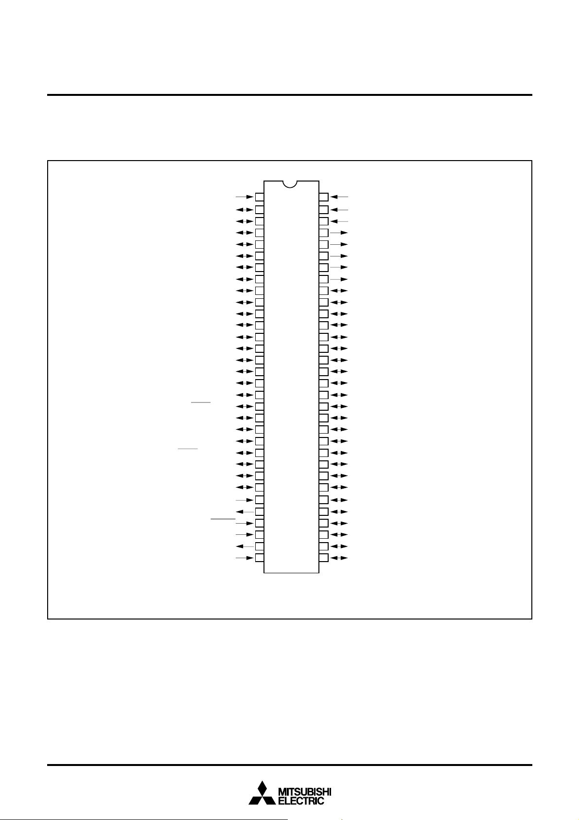
APPENDIX
Pin Configuration (TOP VIEW)
MITSUBISHI MICROCOMPUTERS
M37207MF-XXXSP/FP, M37207M8-XXXSP
M37207EFSP/FP
SINGLE-CHIP 8-BIT CMOS MICROCOMPUTER for VOLTAGE SYNTHESIZER
and ON-SCREEN DISPLAY CONTROLLER
P4
P40/S
P4
P4
1/SCLK2
OSC1/P70/AD4
OSC2/P7
P3
6
/INT2/AD2
P3
P3
D-A/AD3
0
/PWM0
P6
1
/PWM1
P6
P62/PWM2
P6
3
/PWM3
4
/PWM4
P6
P65/PWM5
P6
6
/PWM6
7
/PWM7
P6
P3
2
/TIM2/AD6
P3
P47/
S
RDY1
/PWM8
6/SIN1
5/SCLK1
4/SOUT1
RDY2
/SCL2/AD7
/SDA2/AD8
/PWM9
P4
P4
P4
3
/
S
2/SIN2
/SCL3/X
OUT2
/SDA3/X
CNV
1
/AD5
5
/AD1
4
/INT1
3
/TIM3
P3
P3
/SCL1
/SDA1
COUT
CIN
RESET
X
X
OUT
V
SS
SS
1
2
3
4
5
6
7
8
9
M37207EFSP
10
11
12
13
14
15
16
17
1
18
0
19
20
21
22
23
24
25
26
27
28
φ
29
30
IN
31
32
64
V
CC
63
H
SYNC
62
V
SYNC
61
R/P5
2
60
G/P5
3
59
B/P5
4
58
I/P55/TIM1 OVERFLOW
57
56
M37207MF-XXXSP, M37207M8-XXXSP
55
54
53
52
51
50
49
48
47
46
45
44
43
42
41
40
39
38
37
36
35
34
33
OUT/P5
P0
0
P0
1
P0
2
P0
3
P0
4
P0
5
P0
6
P0
7
P1
0
P1
1
P1
2
P1
3
P1
4
P1
5
P1
6
P1
7
P2
0
P2
1
P2
2
P2
3
P2
4
P2
5
P2
6
P2
7
6
Outline 64P4B
93
Page 94

Pin Configuration (TOP VIEW)
NC
64
NC
B/P5
G/P5
R/P5
V
SYNC
H
SYNC
NC
V
NC
OSC1/P70/AD4
OSC2/P7
1
/AD5
NC
6
/INT2/AD2
P3
5
/AD1
P3
P3
4
/INT1
D-A/AD3
CC
65
4
66
67
3
68
2
69
70
71
72
73
74
75
76
77
78
79
80
1
MITSUBISHI MICROCOMPUTERS
M37207MF-XXXSP/FP, M37207M8-XXXSP
M37207EFSP/FP
SINGLE-CHIP 8-BIT CMOS MICROCOMPUTER for VOLTAGE SYNTHESIZER
6
/TIM1 OVERFLOW
5
I/P5
63
0
P0
OUT/P5
62
61
3
1
2
P0
P0
P0
59
60
58
4
P0
57
56
5
P0
6
7
NC
P0
NC
P0
55
54
NC
53
52
51
M37207MF-XXXFP, M37207EFFP
4
2
5
3
7
6
9
8
10
13
14
12
11
and ON-SCREEN DISPLAY CONTROLLER
2
P1
48
47
18
3
P1
4
P1
46
19
5
P1
45
20
6
P1
44
21
7
P1
43
22
0
P2
42
23
1
P2
41
40
39
38
37
36
35
34
33
32
31
30
29
28
27
26
25
24
0
1
P1
P1
50
49
151617
NC
NC
P2
2
P2
3
P2
4
P2
5
P2
6
P2
7
V
SS
OUT
X
X
IN
RESET
φ
CNV
SS
NC
NC
NC
NC
/PWM0
/PWM1
0
1
P6
P6
/PWM2
/PWM3
2
3
P6
P6
NC
NC
/TIM3
/PWM4
/PWM5
4
5
P6
P6
/PWM6
/PWM7
6
7
P6
P6
3
P3
Outline 80P6N-A
1
0
P3
P3
/TIM2/AD6
2
P3
/PWM8
/PWM9
IN1
RDY1
/S
S
6
/
7
P4
P4
/SCL1
/SDA1
CLK1
OUT1
/S
/S
5
4
P4
P4
CIN
COUT
/SCL2/AD7
RDY2
S
/
3
P4
/SDA3/X
/SDA2/AD8
/SCL3/X
IN2
OUT2
/S
2
CLK2
/S
P4
1
P4φ/S
P4
NC: Unconnected
94
Page 95

Memory Map
MITSUBISHI MICROCOMPUTERS
M37207MF-XXXSP/FP, M37207M8-XXXSP
M37207EFSP/FP
SINGLE-CHIP 8-BIT CMOS MICROCOMPUTER for VOLTAGE SYNTHESIZER
and ON-SCREEN DISPLAY CONTROLLER
RAM
(960 bytes)
for M37207MF
ROM
(62 K bytes)
for M37207MF
RAM
(512 bytes)
for M37207M8
RAM
for display
(144 bytes)
(See note)
ROM
(32 K bytes)
for M37207M8
000016
00C016
00FF16
01FF16
020416
021B16
02C016
02FF16
030016
033F16
04FF16
060016
06D716
080016
800016
FF0016
FFDE16
FFFF
SFR area
Not used
2 page register
Not used
Not used
Not used
Interrupt vector area
16
Zero page
ROM
for display
(12 K bytes)
for M37207MF
ROM correction memory (64 bytes)
Block 1: addresses 02C0
Block 2: addresses 02E016 to 02FF16
Special page
for display
(8 K bytes)
for M37207M8
ROM
16 to 02DF16
10000
16
11FFF16
12FFF16
1FFFF16
Not used
Note: Refer to Table 9. Contents of CRT display RAM.
95
Page 96

M37207MF-XXXSP/FP, M37207M8-XXXSP
SINGLE-CHIP 8-BIT CMOS MICROCOMPUTER for VOLTAGE SYNTHESIZER
Memory Map of Special Function Register (SFR)
■SFR Area (addresses C016 to DF16)
<Bit allocation>
:
Function bit
Name
:
: No function bit
: Fix this bit to “0”
0
(do not write “1”)
: Fix this bit to “1”
1
(do not write “0”)
MITSUBISHI MICROCOMPUTERS
M37207EFSP/FP
and ON-SCREEN DISPLAY CONTROLLER
<State immediately after reset>
: “0” immediately after reset
0
1
: “1” immediately after reset
: Undefined immediately
?
after reset
Address
Port P0 (P0)
C0
16
Port P0 direction register (D0)
C1
16
Port P1 (P1)
C2
16
Port P1 direction register (D1)
C3
16
Port P2 (P2)
C4
16
Port P2 direction register (D2)
C5
16
Port P3 (P3)
C6
16
Port P3 direction register (D3)
C7
16
C8
16
Port P4 (P4)
Port P4 direction register (D4)
C9
16
Port P5 (P5)
CA
16
Port P5 control register (D5)
CB
16
CC
16
Port P6 (P6)
Port P6 direction register (D6)
CD
16
DA-H register (DA-H)
CE
16
DA-L register (DA-L)
CF
16
PWM0 register (PWM0)
D0
16
PWM1 register (PWM1)
D1
16
PWM2 register (PWM2)
D2
16
PWM3 register (PWM3)
D3
16
PWM4 register (PWM4)
D4
16
PWM output control register 1 (PW)
D5
16
PWM output control register 2 (PN)
D6
16
Interrupt interval determination register (??)
D7
16
Interrupt interval determination control register (RE)
D8
16
D9
DA
DB
DC
DD
DE
DF
2
16
C data shift register (S0)
I
16
I2C address register (S0D)
16
I2C status register (S1)
16
I2C control register (S1D)
16
I2C clock control register (S2)
16
Serial I/O mode register (SM)
16
Serial I/O regsiter (SIO)
Register
b7 b0
ACK
Bit allocation State immediately after reset
PW0PW1PW2PW3PW4PW5PW6PW7
PN2PN3PN4
PN1 PN0
RE1RE2RE3RE4RE5 RE0
D1D2D3D4D5D6D7 D0
SAD0SAD1SAD2SAD3SAD4SAD5SAD6
RBW
LRBAD0AASALPINBBTRXMST
BC0BC1BC2ESOALS
CCR0CCR1CCR2CCR3CCR4
SM0SM1SM2SM3SM5SM6
BSEL0BSEL1
ACK
BIT
10BIT
SAD
FAST
MODE
0
b7 b0
?
16
00
?
16
00
?
16
00
??0
00
16
?????
?
?
0
?
00
????
16
?
?
?
00
16
?
00
??????
?
?
?
?
?
16
00
16
00
?
00
16
?
00
16
00 0 010 0?
00
16
00
16
00
16
?
96
Page 97

■
SFR Area (addresses E0
MITSUBISHI MICROCOMPUTERS
M37207MF-XXXSP/FP, M37207M8-XXXSP
M37207EFSP/FP
SINGLE-CHIP 8-BIT CMOS MICROCOMPUTER for VOLTAGE SYNTHESIZER
16
to FF16)
and ON-SCREEN DISPLAY CONTROLLER
Address
E0
16
E1
16
E2
16
E3
16
E4
16
E5
16
E6
16
E7
16
E8
16
E9
16
EA
16
EB
16
EC
16
ED
16
EE
16
EF
16
F0
16
F1
16
F2
16
F3
16
F4
16
F5
16
F6
16
F7
16
F8
16
F9
16
FA
16
FB
16
FC
16
FD
16
FE
16
FF
16
Register
Horizontal register (HR)
Vertical register 1 (CV1)
Vertical register 2 (CV2)
Vertical register 3 (CV3)
Character size register (CS)
Border selection register (MD)
Color register 0 (CO0)
Color register 1 (CO1)
Color register 2 (CO2)
Color register 3 (CO3)
CRT control register 1 (CC)
Display block counter (CBC)
CRT port control register (CRTP)
Wipe mode register (SL)
Wipe start register (??)
A-D control register 1 (ADM)
Timer 1 (TM1)
Timer 2 (TM2)
Timer 3 (TM3)
Timer 4 (TM4)
Timer mode register 1 (TMR1)
Timer mode register 2 (TMR2)
PWM5 register (PWM5)
PWM6 register (PWM6)
PWM7 register (PWM7)
PWM8 register (PWM8)
PWM9 register (PWM9)
CPU mode register (CPUM)
Interrupt request register 1 (IREQ1)
Interrupt request register 2 (IREQ2)
Interrupt control register 1 (ICON1)
Interrupt control register 2 (ICON2)
<Bit allocation>
:
Function bit
Name
:
: No function bit
: Fix this bit to “0”
0
(do not write “1”)
: Fix this bit to “1”
1
(do not write “0”)
b7 b0
0
CS7
CO07
CO17
CO27
CO37
0
CM7 CM6 CM5
0
Bit allocation State immediately after reset
HR0HR1HR2HR3HR4HR5
CV10CV11CV12CV13CV14CV15CV16
CV20CV21CV22CV23CV24CV25CV26
CV30CV31CV32CV33CV34CV35CV36
CS10CS11CS20CS21
MD11MD21MD31MD30
MD10MD20
CO00
CO01CO02CO03CO05
CO11
CO11CO12CO13CO15
CO22
CO21CO22CO23CO25
CO33
CO31CO32CO33CO35
CC0CC1CC2
VSYC
HSYC
SL0SL1
ADM0ADM1ADM2ADM4
TMR10TMR11TMR12TMR13TMR14
TMR20TMR21TMR22TMR23TMR24TMR25TMR26TMR27
00
TM1RTM2RTM3RTM4RCRTRVSCRIICR
IT1RIT2R
TM1ETM2ETM3ETM4ECRTEVSCEIICE
IT1EIT2E
CO06
CO16
CO26
CO36
TMR15TMR16TMR17
TM56R
TM56ETM56C
CS30CS31
CO04
CO14
CO24
CO34
CC3CC4CC5CC6
IRGB
11
CK0MSR
R/G/B
SL2SL3SL4SL5SL6
CM2
S1R
SIEMSE
00
<State immediately after reset>
: “0” immediately after reset
0
: “1” immediately after reset
1
: Undefined immediately
?
after reset
b7 b0
00
16
0
??????
?
?0??????
?0??????
00??
00??? ?
00 000 00
????
??
00
16
00
16
00
16
00
16
00
16
00
16
00
16
00
16
00
16
?
FF
16
07
16
FF
16
07
16
00
16
00
16
?
?
?
?
?
0111 0010
CK0
00
00
00
00
16
16
16
16
97
Page 98

M37207MF-XXXSP/FP, M37207M8-XXXSP
SINGLE-CHIP 8-BIT CMOS MICROCOMPUTER for VOLTAGE SYNTHESIZER
■SFR Area (addresses 20416 to 21B16)
MITSUBISHI MICROCOMPUTERS
M37207EFSP/FP
and ON-SCREEN DISPLAY CONTROLLER
Address
16
204
205
16
206
16
207
16
208
16
209
16
20A
16
20B
16
20C
16
20D
16
20E
16
20F
16
210
16
211
16
212
16
213
16
214
16
215
16
216
16
217
16
218
16
219
16
21A
16
21B
16
<Bit allocation>
Name
0
1
Register
Timer 5 (T5)
Timer 6 (T6)
Port control register (P7D)
Serial I/O control register (SIC)
CRT control register 2 (CBR)
CRT clock selection register (OP)
A-D control register (ADC)
Timer mode register (TMR3)
ROM correction address 1 (high-order)
ROM correction address 1 (low-order)
ROM correction address 2 (high-order)
ROM correction address 2 (low-order)
ROM correction enable register (RCR)
b7
0
<State immediately after reset>
: “0” immediately after reset
b0
P7D0
SIC0SIC1SIC2SIC3SIC4SIC5SIC8SIC7
CBR0CBR1
ADC0ADC1ADC2ADC3ADC4ADC5
TMR30
0
1
: “1” immediately after reset
: Undefined immediately
?
after reset
b7
00
16
00
16
0000
00
16
00
16
00
16
00??
00
16
:
Function bit
:
: No function bit
: Fix this bit to “0”
(do not write “1”)
: Fix this bit to “1”
(do not write “0”)
Bit allocation State immediately after reset
P7D1P7D2P7D4
OP1OP0
?
?
?
?
?
?
?
?
?
?
?
00
16
00
16
00
16
00
16
00
RC1RC0
????
00
??
0
0
b0
??
??
00
98
Page 99

M37207MF-XXXSP/FP, M37207M8-XXXSP
SINGLE-CHIP 8-BIT CMOS MICROCOMPUTER for VOLTAGE SYNTHESIZER
Internal State of Processor Status Register and Program Counter at Reset
<
Bit allocation>
:
Function bit
Name
:
: No function bit
: Fix this bit to “0”
0
(do not write “1”)
: Fix this bit to “1”
1
(do not write “0”)
Register
b7
Processor status register (PS)
Program counter (PCH)
Program counter (PCL)
Bit allocation State immediately after reset
MITSUBISHI MICROCOMPUTERS
M37207EFSP/FP
and ON-SCREEN DISPLAY CONTROLLER
<
State immediately after reset>
: “0” immediately after reset
0
1
: “1” immediately after reset
: Undefined immediately
?
after reset
b0
b7
I ZCDBTVN?????
1
Contents of address FFFF
Contents of address FFFE
b0
??
16
16
99
Page 100

M37207MF-XXXSP/FP, M37207M8-XXXSP
SINGLE-CHIP 8-BIT CMOS MICROCOMPUTER for VOLTAGE SYNTHESIZER
Structure of Register
The figure of each register structure describes its functions, contents
at reset, and attributes as follows:
MITSUBISHI MICROCOMPUTERS
M37207EFSP/FP
and ON-SCREEN DISPLAY CONTROLLER
[Example]
CPU Mode Register
b7b6 b5b4b3 b2b1b0
100
1
Bits
Bit attributes
Values immediately after reset release
CPU mode register (CPUM) (CM) [Address FB
B
Processor mode bits
0, 1
(CM0, CM1)
Stack page selection
2
bit (Note) (CM2)
3, 4
5 Nothing is assigned. This bit is write disable bit.
Clock switch bits
6, 7 0
(CM6, CM7)
: Bit in which nothing is assigned
Name Functions
b1 b0
0 0: Single-chip mode
0 1:
1 0: Not available
1 1:
0: 0 page
1: 1 page
Fix these bits to “1.”
When this bit is read out, the value is “0.”
b7 b6
0 0: f(X
0 1: f(X
1 0: f(X
1 1: Do not set
IN
) = 8 MHz
IN
) = 12 MHz
IN
) = 16 MHz
16]
After reset
(Note 1)
0
0
1
1
(Note 2)
RW
RW
RW
RW
RW
RW
Notes 1: Values immediately after reset release
0••••••“0” after reset release
1••••••“1” after reset release
?••••••Indeterminate after reset release
2: Bit attributes••••••The attributes of control register bits are classified into 3 types : read-only, write-only
and read and write. In the figure, these attributes are represented as follows :
R••••••Read
••••••Read enabled
••••••Read disabled
✕
W••••••Write
✕
✽
••••••Write enabled
••••••Write disabled
••••••“0” can be set by software, but “1”
cannot be set.
100
 Loading...