

Page 1

1/62
PRELIMINARY DATA
November 2002
This is preliminary information on a new product now in development or undergoing evaluation. Details are subject to change without notice.
M36W216TI
M36W216BI
16 Mbit (1Mb x16, Boot Block) Flash Memory
and 2 Mbit (128Kb x16) SRAM, Multiple Memory Product
FEATURES SUMMARY
■ MULTIPLE MEMORY PRODUCT
– 16 Mbit (1Mb x 16) Boot Block Flash Memory
– 2 Mbit (128Kb x 16) SRAM
■ SUPPLY VOLTAGE
–V
DDF
= V
DDS
= 2.7V to 3.3V
–V
DDQF
= V
DDS
= 2.7V to 3.3V
–V
PPF
= 12V for Fast Program (optional)
■ ACCESS TIME: 70ns, 85ns
■ LOW POWER CONSUMPTION
■ ELECTRONIC SIGNATURE
– Manufacturer Code: 20h
– Top Device Code, M36W216TI: 88CEh
– Bottom Device Code, M36W216BI: 88CFh
FLASH MEMORY
■ MEMORY BLOCKS
– Parameter Blocks (Top or Bottom location)
– Main Blocks
■ PROGRAMMING TIME
– 10µs typical
– Double Word Programming Option
■ BLOCK LOCKING
– All blocks locked at Power up
– Any combination of blocks can be locked
–WP
F
for Block Lock-Down
■ AUTOMATIC STAND-BY MODE
■ PROGRAM and ERASE SUSPEND
■ 100,000 PROGRAM/ERASE CYCLES per
BLOCK
■ COMMON FLASH INTERFACE
– 64 bit Security Code
■ SECURITY
– 64 bit user programmable OTP cells
– 64 bit unique device identifier
– One parameter block permanently lockable
SRAM
■ 2 Mbit (128K x 16 bit)
■ ACCESS TIME: 70ns
■ LOW V
DDS
DATA RETENTION: 1.5V
■ POWER DOWN FEATURES USING TWO
CHIP ENABLE INPUTS
Figure 1. Packages
FBGA
Stacked LFBGA66 (ZA)
12 x 8mm
Page 2

M36W216TI, M36W216BI
2/62
TABLE OF CONTENTS
SUMMARY DESCRIPTION. . . . . . . . . . . . . . . . . . . . . . . . . . . . . . . . . . . . . . . . . . . . . . . . . . . . . . . . . . . 6
Figure 2. Logic Diagram . . . . . . . . . . . . . . . . . . . . . . . . . . . . . . . . . . . . . . . . . . . . . . . . . . . . . . . . . . 6
Table 1. Signal Names . . . . . . . . . . . . . . . . . . . . . . . . . . . . . . . . . . . . . . . . . . . . . . . . . . . . . . . . . . . 6
Figure 3. LFBGA Connections (Top view through package). . . . . . . . . . . . . . . . . . . . . . . . . . . . . . . 7
SIGNAL DESCRIPTION . . . . . . . . . . . . . . . . . . . . . . . . . . . . . . . . . . . . . . . . . . . . . . . . . . . . . . . . . . . . . 8
Address Inputs (A0-A16). . . . . . . . . . . . . . . . . . . . . . . . . . . . . . . . . . . . . . . . . . . . . . . . . . . . . . . . . . 8
Address Inputs (A17-A19). . . . . . . . . . . . . . . . . . . . . . . . . . . . . . . . . . . . . . . . . . . . . . . . . . . . . . . . . 8
Data Inputs/Outputs (DQ0-DQ15). . . . . . . . . . . . . . . . . . . . . . . . . . . . . . . . . . . . . . . . . . . . . . . . . . . 8
Flash Chip Enable (EF). . . . . . . . . . . . . . . . . . . . . . . . . . . . . . . . . . . . . . . . . . . . . . . . . . . . . . . . . . . 8
Flash Output Enable (GF). . . . . . . . . . . . . . . . . . . . . . . . . . . . . . . . . . . . . . . . . . . . . . . . . . . . . . . . . 8
Flash Write Enable (WF). . . . . . . . . . . . . . . . . . . . . . . . . . . . . . . . . . . . . . . . . . . . . . . . . . . . . . . . . . 8
Flash Write Protect (WPF). . . . . . . . . . . . . . . . . . . . . . . . . . . . . . . . . . . . . . . . . . . . . . . . . . . . . . . . . 8
Flash Reset (RPF). . . . . . . . . . . . . . . . . . . . . . . . . . . . . . . . . . . . . . . . . . . . . . . . . . . . . . . . . . . . . . . 8
SRAM Chip Enable (E1S, E2S). . . . . . . . . . . . . . . . . . . . . . . . . . . . . . . . . . . . . . . . . . . . . . . . . . . . . 8
SRAM Write Enable (WS). . . . . . . . . . . . . . . . . . . . . . . . . . . . . . . . . . . . . . . . . . . . . . . . . . . . . . . . . 8
SRAM Output Enable (GS).. . . . . . . . . . . . . . . . . . . . . . . . . . . . . . . . . . . . . . . . . . . . . . . . . . . . . . . . 8
SRAM Upper Byte Enable (UBS). . . . . . . . . . . . . . . . . . . . . . . . . . . . . . . . . . . . . . . . . . . . . . . . . . . . 8
SRAM Lower Byte Enable (LBS). . . . . . . . . . . . . . . . . . . . . . . . . . . . . . . . . . . . . . . . . . . . . . . . . . . . 8
V
DDF
and VDDS Supply Voltages.. . . . . . . . . . . . . . . . . . . . . . . . . . . . . . . . . . . . . . . . . . . . . . . . . . . 8
V
DDQF
and V
DDS
Supply Voltage (2.7V to 3.3V). . . . . . . . . . . . . . . . . . . . . . . . . . . . . . . . . . . . . . . . 8
V
PPF
Program Supply Voltage. . . . . . . . . . . . . . . . . . . . . . . . . . . . . . . . . . . . . . . . . . . . . . . . . . . . . . 8
V
SSF
and V
SSS
Ground.. . . . . . . . . . . . . . . . . . . . . . . . . . . . . . . . . . . . . . . . . . . . . . . . . . . . . . . . . . . 9
FUNCTIONAL DESCRIPTION . . . . . . . . . . . . . . . . . . . . . . . . . . . . . . . . . . . . . . . . . . . . . . . . . . . . . . . . 9
Figure 4. Functional Block Diagram . . . . . . . . . . . . . . . . . . . . . . . . . . . . . . . . . . . . . . . . . . . . . . . . . 9
Table 2. Main Operation Modes . . . . . . . . . . . . . . . . . . . . . . . . . . . . . . . . . . . . . . . . . . . . . . . . . . . 10
MAXIMUM RATING. . . . . . . . . . . . . . . . . . . . . . . . . . . . . . . . . . . . . . . . . . . . . . . . . . . . . . . . . . . . . . . . 11
Table 3. Absolute Maximum Ratings. . . . . . . . . . . . . . . . . . . . . . . . . . . . . . . . . . . . . . . . . . . . . . . .11
DC AND AC PARAMETERS. . . . . . . . . . . . . . . . . . . . . . . . . . . . . . . . . . . . . . . . . . . . . . . . . . . . . . . . . 1 2
Table 4. Operating and AC Measurement Conditions. . . . . . . . . . . . . . . . . . . . . . . . . . . . . . . . . . . 12
Figure 5. AC Measurement I/O Waveform . . . . . . . . . . . . . . . . . . . . . . . . . . . . . . . . . . . . . . . . . . .12
Figure 6. AC Measurement Load Circuit . . . . . . . . . . . . . . . . . . . . . . . . . . . . . . . . . . . . . . . . . . . . . 12
Table 5. Device Capaci ta n ce. . . . . . . . . . . . . . . . . . . . . . . . . . . . . . . . . . . . . . . . . . . . . . . . . . . . . . 12
Table 6. DC Character i stics. . . . . . . . . . . . . . . . . . . . . . . . . . . . . . . . . . . . . . . . . . . . . . . . . . . . . . . 13
PACKAGE MECHANICAL . . . . . . . . . . . . . . . . . . . . . . . . . . . . . . . . . . . . . . . . . . . . . . . . . . . . . . . . . . 15
Figure 7. Stacked LFBGA66-12x8mm , 8x8 ball array, 0.8mm pitch, Bottom Vi ew Package Ou tline15
Table 7. Stacked LFBGA66 - 12x8mm, 8x8 ball array, 0.8 mm pitch, Package Mechanical Data . 15
Figure 8. Stacked LFBGA66 Daisy Chain - Package Connections (Top view through package) . . 16
Figure 9. Stac k ed LFBGA6 6 Daisy C hain - PC B Connect ions proposal (Top view through package).17
Page 3

3/62
M36W216TI, M36W216BI
PART NUMBERING . . . . . . . . . . . . . . . . . . . . . . . . . . . . . . . . . . . . . . . . . . . . . . . . . . . . . . . . . . . . . . . 18
Table 8. Ordering Information Scheme . . . . . . . . . . . . . . . . . . . . . . . . . . . . . . . . . . . . . . . . . . . . . . 18
Table 9. Daisy Chain Orde r ing Scheme . . . . . . . . . . . . . . . . . . . . . . . . . . . . . . . . . . . . . . . . . . . . . 18
FLASH DEVICE. . . . . . . . . . . . . . . . . . . . . . . . . . . . . . . . . . . . . . . . . . . . . . . . . . . . . . . . . . . . . . . . . . . 19
FLASH SUMMARY DESCRIPTION. . . . . . . . . . . . . . . . . . . . . . . . . . . . . . . . . . . . . . . . . . . . . . . . 19
Figure 10. Flash Block Ad d re sse s . . . . . . . . . . . . . . . . . . . . . . . . . . . . . . . . . . . . . . . . . . . . . . 20
Figure 11. Flash Security Block and Protection Register Memory Map . . . . . . . . . . . . . . . . . . 20
FLASH BUS OPERATIONS. . . . . . . . . . . . . . . . . . . . . . . . . . . . . . . . . . . . . . . . . . . . . . . . . . . . . . 21
Read.. . . . . . . . . . . . . . . . . . . . . . . . . . . . . . . . . . . . . . . . . . . . . . . . . . . . . . . . . . . . . . . . . . . . . 2 1
Write.. . . . . . . . . . . . . . . . . . . . . . . . . . . . . . . . . . . . . . . . . . . . . . . . . . . . . . . . . . . . . . . . . . . . . 21
Output Disable.. . . . . . . . . . . . . . . . . . . . . . . . . . . . . . . . . . . . . . . . . . . . . . . . . . . . . . . . . . . . . 21
Standby. . . . . . . . . . . . . . . . . . . . . . . . . . . . . . . . . . . . . . . . . . . . . . . . . . . . . . . . . . . . . . . . . . . 21
Automatic Standby.. . . . . . . . . . . . . . . . . . . . . . . . . . . . . . . . . . . . . . . . . . . . . . . . . . . . . . . . . . 21
Reset. . . . . . . . . . . . . . . . . . . . . . . . . . . . . . . . . . . . . . . . . . . . . . . . . . . . . . . . . . . . . . . . . . . . . 21
FLASH COMMAND INTERFACE. . . . . . . . . . . . . . . . . . . . . . . . . . . . . . . . . . . . . . . . . . . . . . . . . . 22
Read Memory Array Command. . . . . . . . . . . . . . . . . . . . . . . . . . . . . . . . . . . . . . . . . . . . . . . . . . . .22
Read Status Register Command. . . . . . . . . . . . . . . . . . . . . . . . . . . . . . . . . . . . . . . . . . . . . . . . . . .22
Read Electronic Signature Comma nd . . . . . . . . . . . . . . . . . . . . . . . . . . . . . . . . . . . . . . . . . . . . . . . 22
Read CFI Query Command. . . . . . . . . . . . . . . . . . . . . . . . . . . . . . . . . . . . . . . . . . . . . . . . . . . . . . . 2 2
Block Erase Command . . . . . . . . . . . . . . . . . . . . . . . . . . . . . . . . . . . . . . . . . . . . . . . . . . . . . . . . . . 22
Program Command. . . . . . . . . . . . . . . . . . . . . . . . . . . . . . . . . . . . . . . . . . . . . . . . . . . . . . . . . . . . . 22
Double Word Program Command . . . . . . . . . . . . . . . . . . . . . . . . . . . . . . . . . . . . . . . . . . . . . . . . . . 23
Clear Status Regist e r Command. . . . . . . . . . . . . . . . . . . . . . . . . . . . . . . . . . . . . . . . . . . . . . . . . . . 23
Program/Erase Suspend Comm and . . . . . . . . . . . . . . . . . . . . . . . . . . . . . . . . . . . . . . . . . . . . . . . . 23
Program/Eras e Resume Command . . . . . . . . . . . . . . . . . . . . . . . . . . . . . . . . . . . . . . . . . . . . . . . . 23
Protection Regi ste r Pr o g ra m Comman d . . . . . . . . . . . . . . . . . . . . . . . . . . . . . . . . . . . . . . . . . . . . . 23
Block Lock Command . . . . . . . . . . . . . . . . . . . . . . . . . . . . . . . . . . . . . . . . . . . . . . . . . . . . . . . . . . . 24
Block Unlock Command . . . . . . . . . . . . . . . . . . . . . . . . . . . . . . . . . . . . . . . . . . . . . . . . . . . . . . . . . 2 4
Block Lock-Down Command. . . . . . . . . . . . . . . . . . . . . . . . . . . . . . . . . . . . . . . . . . . . . . . . . . . . . . 24
Table 10. Flash Commands . . . . . . . . . . . . . . . . . . . . . . . . . . . . . . . . . . . . . . . . . . . . . . . . . . . 25
Table 11. Read Electronic Signature . . . . . . . . . . . . . . . . . . . . . . . . . . . . . . . . . . . . . . . . . . . . 25
Table 12. Read Block Lock Signature. . . . . . . . . . . . . . . . . . . . . . . . . . . . . . . . . . . . . . . . . . . . 26
Table 13. Read Protection Register and Lock Register . . . . . . . . . . . . . . . . . . . . . . . . . . . . . . 26
Table 14. Program, Erase Times and Program/E rase Endu ranc e Cycles . . . . . . . . . . . . . . . . 26
FLASH BLOCK LOCKING . . . . . . . . . . . . . . . . . . . . . . . . . . . . . . . . . . . . . . . . . . . . . . . . . . . . . .27
Reading a Block’s Lock Status . . . . . . . . . . . . . . . . . . . . . . . . . . . . . . . . . . . . . . . . . . . . . . . . . . . . 27
Locked State . . . . . . . . . . . . . . . . . . . . . . . . . . . . . . . . . . . . . . . . . . . . . . . . . . . . . . . . . . . . . . . . . . 27
Unlocked State . . . . . . . . . . . . . . . . . . . . . . . . . . . . . . . . . . . . . . . . . . . . . . . . . . . . . . . . . . . . . . . . 27
Lock-Down State. . . . . . . . . . . . . . . . . . . . . . . . . . . . . . . . . . . . . . . . . . . . . . . . . . . . . . . . . . . . . . . 27
Locking Operatio n s Durin g Erase Su sp e nd . . . . . . . . . . . . . . . . . . . . . . . . . . . . . . . . . . . . . . . . . . 27
Table 15. Block Lock Status . . . . . . . . . . . . . . . . . . . . . . . . . . . . . . . . . . . . . . . . . . . . . . . . . . .28
Table 16. Protection Status. . . . . . . . . . . . . . . . . . . . . . . . . . . . . . . . . . . . . . . . . . . . . . . . . . . . 28
Page 4

M36W216TI, M36W216BI
4/62
FLASH STATUS REGISTER . . . . . . . . . . . . . . . . . . . . . . . . . . . . . . . . . . . . . . . . . . . . . . . . . . . . . 29
Program/Erase Controller Status (Bit 7) . . . . . . . . . . . . . . . . . . . . . . . . . . . . . . . . . . . . . . . . . .29
Erase Suspend Status (Bit 6) . . . . . . . . . . . . . . . . . . . . . . . . . . . . . . . . . . . . . . . . . . . . . . . . . .29
Erase Status (Bit 5). . . . . . . . . . . . . . . . . . . . . . . . . . . . . . . . . . . . . . . . . . . . . . . . . . . . . . . . . . 29
Program Status (Bit 4). . . . . . . . . . . . . . . . . . . . . . . . . . . . . . . . . . . . . . . . . . . . . . . . . . . . . . . . 29
V
PP
Status (Bit 3) . . . . . . . . . . . . . . . . . . . . . . . . . . . . . . . . . . . . . . . . . . . . . . . . . . . . . . . . . . . 29
Program Suspend Status (Bit 2). . . . . . . . . . . . . . . . . . . . . . . . . . . . . . . . . . . . . . . . . . . . . . . . 29
Block Protection Status (Bit 1) . . . . . . . . . . . . . . . . . . . . . . . . . . . . . . . . . . . . . . . . . . . . . . . . .30
Reserved (Bit 0) . . . . . . . . . . . . . . . . . . . . . . . . . . . . . . . . . . . . . . . . . . . . . . . . . . . . . . . . . . . . 3 0
Table 17. Status Register Bits. . . . . . . . . . . . . . . . . . . . . . . . . . . . . . . . . . . . . . . . . . . . . . . . . .30
Figure 12. Flash Read Mode AC Waveforms . . . . . . . . . . . . . . . . . . . . . . . . . . . . . . . . . . . . . . 31
Table 18. Flash Read AC Characteristics. . . . . . . . . . . . . . . . . . . . . . . . . . . . . . . . . . . . . . . . . 31
Figure 13. Flash Write AC Wavefo r ms, Write Enable Control l e d . . . . . . . . . . . . . . . . . . . . . . . 32
Table 19. Flash Write AC Chara cte ristics, Write En a ble Controlled. . . . . . . . . . . . . . . . . . . . . 33
Figure 14. Flash Write AC Waveforms, Chip Enable Controlled . . . . . . . . . . . . . . . . . . . . . . . . 34
Table 20. Flash Write AC Characteristics, Chip Enable Controlled . . . . . . . . . . . . . . . . . . . . . 35
Figu r e 1 5 . Flash Power -Up an d R e set AC W a veforms. . . . . . . . . . . . . . . . . . . . . . . . . . . . . . . 36
Table 21. Flash Power-Up and Reset AC Characteristics . . . . . . . . . . . . . . . . . . . . . . . . . . . . 36
SRAM DEVICE . . . . . . . . . . . . . . . . . . . . . . . . . . . . . . . . . . . . . . . . . . . . . . . . . . . . . . . . . . . . . . . . . . . 3 7
SRAM SUMMARY DESCRIPTION. . . . . . . . . . . . . . . . . . . . . . . . . . . . . . . . . . . . . . . . . . . . . . . . . 37
Figure 16. SRAM Logic Diagram . . . . . . . . . . . . . . . . . . . . . . . . . . . . . . . . . . . . . . . . . . . . . . .37
SRAM OPERATIONS. . . . . . . . . . . . . . . . . . . . . . . . . . . . . . . . . . . . . . . . . . . . . . . . . . . . . . . . . . . 38
Read . . . . . . . . . . . . . . . . . . . . . . . . . . . . . . . . . . . . . . . . . . . . . . . . . . . . . . . . . . . . . . . . . . . . . 3 8
Write . . . . . . . . . . . . . . . . . . . . . . . . . . . . . . . . . . . . . . . . . . . . . . . . . . . . . . . . . . . . . . . . . . . . . 38
Standby/Power-Down . . . . . . . . . . . . . . . . . . . . . . . . . . . . . . . . . . . . . . . . . . . . . . . . . . . . . . . .38
Data Retention . . . . . . . . . . . . . . . . . . . . . . . . . . . . . . . . . . . . . . . . . . . . . . . . . . . . . . . . . . . . . 38
Output Disable . . . . . . . . . . . . . . . . . . . . . . . . . . . . . . . . . . . . . . . . . . . . . . . . . . . . . . . . . . . . . 3 8
Figure 17. SRAM Read Mode AC Waveforms, Address Controlled with UBS = LBS = V
IL
. . . 39
Figure 18. SRAM Read AC Waveforms, GS Controlled . . . . . . . . . . . . . . . . . . . . . . . . . . . . . . 39
Figure 19. SRAM Standby AC Waveforms . . . . . . . . . . . . . . . . . . . . . . . . . . . . . . . . . . . . . . . . 39
Table 22. SRAM Read AC Characteristics . . . . . . . . . . . . . . . . . . . . . . . . . . . . . . . . . . . . . . . .40
Figure 20. SRAM Write AC Waveforms, WS Controlled. . . . . . . . . . . . . . . . . . . . . . . . . . . . . . 41
Figu r e 2 1 . SRAM Write A C Wav e forms, E1S Con trolle d . . . . . . . . . . . . . . . . . . . . . . . . . . . . . 42
Figure 22. SRAM Write AC Waveforms, WS Controlled with GS Low . . . . . . . . . . . . . . . . . . . 43
Figure 23. SRAM Write Cycle Waveform, UBS and LBS Controlled, GS Low . . . . . . . . . . . . . 43
Table 23. SRAM Write AC Characteristics . . . . . . . . . . . . . . . . . . . . . . . . . . . . . . . . . . . . . . . . 44
Figure 24. SRAM Low V
DDS
Data Retention AC Waveforms, E1S or UBS / LBS Controlled . . 45
Table 24. SRAM Low V
DDS
Data Retention Characte r i stic. . . . . . . . . . . . . . . . . . . . . . . . . . . . 45
APPENDIX A. BLOCK ADDRESS TABLES . . . . . . . . . . . . . . . . . . . . . . . . . . . . . . . . . . . . . . . . . . . . 46
Table 25. Top Boot Block Addresses, M36W216TI. . . . . . . . . . . . . . . . . . . . . . . . . . . . . . . . . . . . . 46
Table 26. Botto m Boo t Bl oc k Addre sse s, M36W216BI. . . . . . . . . . . . . . . . . . . . . . . . . . . . . . . . . . 46
Page 5

5/62
M36W216TI, M36W216BI
APPENDIX B. COMMON FLASH INTERFACE (CFI) . . . . . . . . . . . . . . . . . . . . . . . . . . . . . . . . . . . . . 47
Table 27. Query Stru cture Overview. . . . . . . . . . . . . . . . . . . . . . . . . . . . . . . . . . . . . . . . . . . . . . . .47
Table 28. CFI Query Identification String . . . . . . . . . . . . . . . . . . . . . . . . . . . . . . . . . . . . . . . . . . . .47
Table 29. CFI Query System Interface Information. . . . . . . . . . . . . . . . . . . . . . . . . . . . . . . . . . . . . 48
Table 30. Device Geome try Definition. . . . . . . . . . . . . . . . . . . . . . . . . . . . . . . . . . . . . . . . . . . . . . .49
Table 31. Primary Algorithm-Specific Extended Query Table . . . . . . . . . . . . . . . . . . . . . . . . . . . . . 50
Table 32. Security Code Area . . . . . . . . . . . . . . . . . . . . . . . . . . . . . . . . . . . . . . . . . . . . . . . . . . . . . 51
APPENDIX C. FLOWCHARTS AND PSEUDO CODES. . . . . . . . . . . . . . . . . . . . . . . . . . . . . . . . . . . . 52
Figure 25. Program Flowchart and Pseudo Code . . . . . . . . . . . . . . . . . . . . . . . . . . . . . . . . . . . . . . 52
Figure 26. Double Word Program Flowchart and Pseudo Code . . . . . . . . . . . . . . . . . . . . . . . . . . . 53
Figure 27. Program Suspend & Resume Flowchart and Pseudo Code . . . . . . . . . . . . . . . . . . . . . 54
Figure 28. Erase Flowchart and Pseudo Code . . . . . . . . . . . . . . . . . . . . . . . . . . . . . . . . . . . . . . . . 55
Figure 29. Erase Suspend & Resume Flowchart and Pseudo Code. . . . . . . . . . . . . . . . . . . . . . . . 56
Figure 30. Locking Operations Flowchart and Pseudo Code . . . . . . . . . . . . . . . . . . . . . . . . . . . . . 57
APPENDIX D. COMMAND INTERFACE AND PROGRAM/ERASE CONTROLLER STATE . . . . . . . 59
Table 33. Write State Machine Current/Next, sheet 1 of 2.. . . . . . . . . . . . . . . . . . . . . . . . . . . . . . . 59
Table 34. Write State Machine Current/Next, sheet 2 of 2.. . . . . . . . . . . . . . . . . . . . . . . . . . . . . . . 60
REVISION HISTORY. . . . . . . . . . . . . . . . . . . . . . . . . . . . . . . . . . . . . . . . . . . . . . . . . . . . . . . . . . . . . . . 61
Table 35. Document Revision History. . . . . . . . . . . . . . . . . . . . . . . . . . . . . . . . . . . . . . . . . . . . . . .61
Page 6
M36W216TI, M36W216BI
6/62
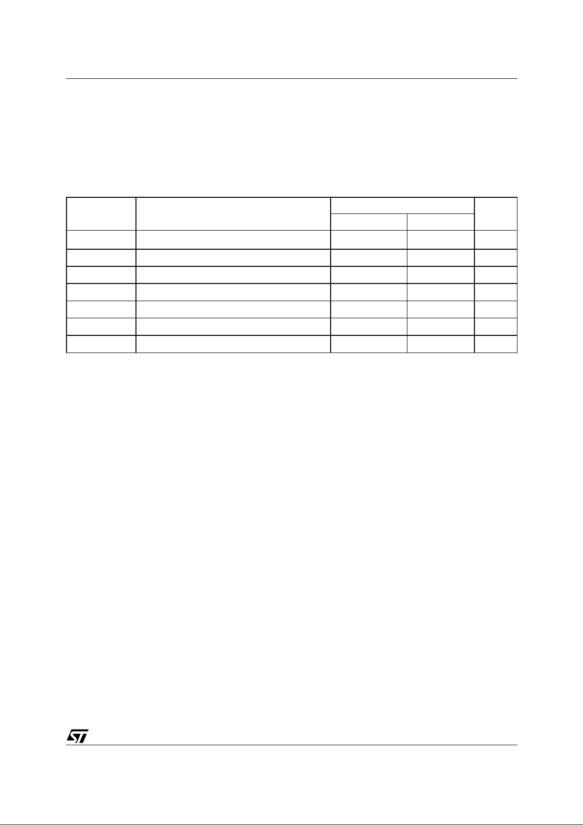
SUMMARY DESCRIPTION
The M36W216TI is a low voltage Multiple Memory
Product which combines two memory devices; a
16 Mbit boot block Flash memory and a 2 Mbit
SRAM. Recommended operating conditions do
not allow both the F lash memory and the S RAM
memory to be active at the same time.
The memory is offered in a Stacked LFBGA66
(12x8mm, 8 x 8 active ball, 0.8 mm pitch) package
and is supplied with all the bits erased (set to ‘1’).
Figure 2. Logic Diagram
Table 1. Signal Names
AI07903
20
A0-A19
E
F
DQ0-DQ15
V
DDF
M36W216TI
M36W216BI
G
F
V
SSF
16
W
F
RP
F
WP
F
V
DDQF
E1
S
G
S
W
S
UB
S
LB
S
V
SSS
V
PPF
V
DDS
E2
S
A0-A16 Flash and SRAM Address Inputs
A17-A19 Address Inputs for Flash Chip only
DQ0-DQ15 Data Input/Output
V
DDF
Flash Power Supply
V
DDQF
Flash Power Supply for I/O Buffers
V
PPF
Flash Optional Supply V oltage for Fast
Program & Erase
V
SSF
Flash Ground
V
DDS
SRAM Power Supply
V
SSS
SRAM Ground
NC Not Connected Internally
Flash control functions
E
F
Chip Enable input
G
F
Output Enable input
W
F
Write Enable input
RP
F
Reset input
WP
F
Write Protect input
SRAM control functions
E1
S
, E2
S
Chip Enable inputs
G
S
Output Enable input
W
S
Write Enable input
UB
S
Upper Byte Enable input
LB
S
Lower Byte Enable input
Page 7
7/62
M36W216TI, M36W216BI
Figure 3. LFBGA Connections (Top view through package)
AI90254
A
654321#2#1
E
B
F
A12
A13A11NCNC
NC
E2SDQ12V
SSS
A2A3A6A7A18
EFA0A4NCNC
DQ4
WS
DQ15A9A16
DQ6DQ13NCWF
A8 A10
A5
NC V
SSF
A17
RPF
A15 A14
NCNC
V
DDF
E1SA1
NCNCGF
V
DDS
DQ7
DQ5
DQ14
NC
V
SSF
V
DDQF
#4#387
C
DQ10
DQ11A19WPF
V
PPF
DQ3DQ2
D
DQ8DQ9GSLBS
UBS
DQ1DQ0
G
H
Page 8

M36W216TI, M36W216BI
8/62
SIGNAL DESCRIPTION
See Figure 2 Logic Diagram and Table 1, Sign al
Names, for a brief overview of the signals connected to this de vice.
Address Inputs (A0-A16). Addresses A0-A16
are common inputs for the Flash an d the SRAM
components. The Address Inputs select the cells
in the memory array to access during Bu s Read
operations. During Bus Write operations they control the commands sent to the Command Interface
of the internal state machine. The Flash memory is
accessed through the Chip Enable (
E
F
) and Write
Enable (W
F
) signals, while the SRAM i s acce sse d
through two Chip Enable ( ES
) and Write Enable
(W
S
) signals.
Address Inputs (A17-A19). Addresses A17-A19
are inputs for the Flash component only. The
Flash memory is acc essed through the Chip E nable (
E
F
) and Write Enable (WF) signals
Data Inputs/Outputs (DQ0-DQ15). The Data I/
O output the d ata stored at the selected addres s
during a Bus Read operation or in put a c om m and
or the data to be programmed durin g a Write Bus
operation.
Flash Chip Enable (
E
F
). The Chip Enable input
activates the Flash memory control logic, input
buffers, decoders and sense amplifiers. When
Chip Enable is at V
IL
and Reset is at VIH the device
is in active mode. When Chip Enable is at V
IH
the
memory is deselected, the outputs are high impedance and the power consumption is reduced to the
standby level.
Flash Output Enable (G
F
). The Output Enable
controls the data outputs during the Bus Read operation of the Flash memory.
Flash Write Enable (
W
F
). The Write Enable con-
trols the Bus Write operation of the Flash m emory’s Command Interface. The data and address
inputs are latched on the rising e dge of Chip Enable,
E
F
, or Write Enable, WF, whichever occurs
first .
Flash Write Protect (WP
F
). Write Protect is an
input that gives an additional hardware protection
for each block. When Write Protect is at V
IL
, the
Lock-Down is enabled and the protection status of
the block cannot be changed. When Write Protect
is at V
IH
, the Lock-Down is disabled and the block
can be locked or unlocked. (refer to T able 6, Read
Protection Register and Protection Register Lock).
Flash Reset (RP
F
). The Reset input provides a
hardware reset of the Flash memory. When Reset
is at V
IL
, the memory is in reset mode: the outputs
are high impedance and the current c onsumption
is minimized. After Reset all blocks are in the
Locked state. When Reset is at V
IH
, the device is
in normal operation. Exiting reset mode the device
enters read array mode, but a negative t ransition
of Chip Enable or a change of the address is required to ensure valid data outputs.
SRAM Chip Enable (E1
S
, E2S). The Chip En-
able inputs activate the SRAM memory control
logic, input buffers and decoders. E1
S
at VIH or
E2
S
at VIL deselects the memory and reduces the
power consumption to the standby level. E1
S
or
E2
S
can also be used to control writing to the
SRAM memory array, while W
S
rema in s at V
IL.
It
is not allowed to set
E
F
at VIL and, E1S at VIL or
E2
S
at VIL at the same time.
SRAM Write Enable (W
S
). The Write Enable in-
put controls writing to the SRA M memory array.
W
S
is active low .
SRAM Output E nable (G
S
). The Output Enable
gates the outputs through the data buffers during
a read operation of the SRAM m emory. G
S
is ac-
tive low.
SRAM Upper Byte Enable (UB
S
). The Upper
Byte Enable enables the upper bytes for SRAM
(DQ8-DQ15). UB
S
is acti v e low.
SRAM Lower Byte Enable (LB
S
). The Lower
Byte Enable enables the lower bytes for SRAM
(DQ0-DQ7). LB
S
is active low.
V
DDF
and V
DDS
Supply Voltages. V
DDF
provides the power supply to the internal core of the
Flash Memory device. It is the main power s upply
for all operations (Read, Program and Erase).
V
DDQF
and V
DDS
Supply Voltage (2.7V to 3.3V).
V
DDQF
provides the power supply for the Flash
memory I/O pins and V
DDS
provides the power
supply for t he SRAM control pins. This a llows all
Outputs to be powered independently of the Flash
core power supply, V
DDF
. V
DDQF
can be tied to
V
DDS.
V
PPF
Program Supp ly Vol tage. V
PPF
is both a
control input and a power suppl y pin for t he F lash
memory. The two functions are selected by the
voltage range applied to the pin. The Supply Voltage V
DDF
and the Program Supply Vol tage V
PPF
can be applied in any order.
If V
PPF
is kept in a low voltage range (0V t o 3.6V)
V
PPF
is seen as a control input. In this case a volt-
age lower than V
PPLK
gives an absolute protection
against program or erase, while V
PPF
> V
PP1
enables these functions (see Table 6, DC Characteristics for the relevant values). V
PPF
is only
sampled at the beginning of a program or erase; a
change in its value after the operation has started
does not have any effect and program or erase operations continue.
If V
PPF
is in the range 11.4V to 12.6V it acts as a
power supply pin. In this condition V
PPF
must be
stable until the Program/Erase algorithm i s completed (see Table 19 and 20).
Page 9
9/62
M36W216TI, M36W216BI
V
SSF
and V
SSS
Ground. V
SSF
and V
SSS
are the
ground reference for all voltage measurements in
the Flash and SRAM chips, respectively.
Note: Each device in a system should have V
D-
DF
, V
DDQF
and V
PPF
decoupled with a 0.1µF ca-
pacitor close to the pin. See Figure 9, AC
Measurement Load Circuit. The PCB trace
widths should be sufficient to carry the required V
PPF
program and erase currents.
FUNCTIONAL DESCRIPTION
The Flash and SRAM components have separate
power supplies and grounds and are distinguished
by three chip enable inputs:
E
F
for the Flash mem-
ory and E1
S
and E2S for the SRAM.
Recommended operating conditions do not allow
both the Flash and the SRAM to be in active mode
at the same time. The most common example is
simultaneous read operations on the Flash and
the SRAM which would resul t in a data bus contention. Therefore it is recommended to put the
SRAM in the h igh impedance state whe n reading
the Flash and vice versa (see Table 2 Main Operation Modes for details).
Figure 4. Func ti onal Block Di a gram
AI07904
Flash Memory
16 Mbit (x16)
V
SSF
E
F
G
F
W
F
RP
F
WP
F
E1
S
G
S
W
S
UB
S
LB
S
DQ0-DQ15
V
DDF
V
PPF
A17-A19
A0-A16
SRAM
2 Mbit (x16)
V
SSS
V
DDS
V
DDQF
E2
S
Page 10
M36W216TI, M36W216BI
10/62
Table 2. Main Operation Modes
Note: X = Don’t care = VIL or VIH, V
PPFH
= 12V ± 5%.
Operation
Mode
E
FGFWF
RPFWP
F
V
PPF
E1SE2SGSWSUBSLB
S
DQ7-DQ0 DQ15-DQ8
Flash Memory
Read
V
ILVILVIHVIH
X Don’t care SRAM must be disabled Data Output
Write
V
ILVIHVILVIH
X
V
DDF
or
V
PPFH
SRAM must be disabled Data Input
Block
Locking
V
IL
XX
V
IH
V
IL
Don’t care SRAM must be disabled X
Standby
V
IH
XX
V
IH
X Don’t care Any SRAM mode is allowed Hi-Z
Reset X X X
V
IL
X Don’t care Any SRAM mode is allowed Hi-Z
Output
Disable
V
ILVIHVIHVIH
X Don’t care Any SRAM mode is allowed Hi-Z
SRAM
Read
Flash must be disabled
V
ILVIHVILVIHVIL
V
IL
Data out Word Read
Flash must be disabled
V
ILVIHVILVIHVIHVIL
Data out Hi-Z
Flash must be disabled
V
ILVIHVILVIHVIL
V
IH
Hi-Z Data out
Write
Flash must be disabled
V
ILVIH
XVILV
IL
V
IL
Data in Word Write
Flash must be disabled
V
ILVIH
XVILV
IHVIL
Data in Hi-Z
Flash must be disabled
V
ILVIH
XVILV
IL
V
IH
Hi-Z Data in
Standby/
Power
Down
Any Flash mode is allowable
V
IHVIL
X X X X Hi-Z
XXXX
V
IHVIH
Hi-Z
Data
Retention
Any Flash mode is allowable
V
IHVIL
X X X X Hi-Z
XXXX
V
IHVIH
Hi-Z
Output
Disable
Any Flash mode is allowable
V
ILVIHVIHVIHVIL
V
IL
Hi-Z
Any Flash mode is allowable
V
ILVIHVIHVIHVIHVIL
Hi-Z
Any Flash mode is allowable
V
ILVIHVIHVIHVIL
V
IH
Hi-Z
Page 11
11/62
M36W216TI, M36W216BI
MAXIMUM RATIN G
Stressing the device above the rating l isted in the
Absolute Maximum Ratings table m ay cause permanent damage to the device. These are stress
ratings only and operation of the device at t hese or
any other conditions ab ove those i ndicated in t he
Operating sections of this specificat ion is not im-
plied. Exposure to Absolute Maximum Rating conditions for extended periods may affect device
reliability. Refer also to the STMicroelectronics
SURE Program and other relevant quality documents.
Table 3. Absolute Maximum Ratings
Note: 1. Depends on range.
Symbol Parameter
Value
Unit
Min Max
T
A
Ambient Operating Temperature
(1)
–40 85 °C
T
BIAS
Temperature Under Bias –40 125 °C
T
STG
Storage Temperature –55 150 °C
V
IO
Input or Output Voltage –0.5
V
DDQF
+0.5
V
V
DDF
, V
DDQF
Flash Supply Voltage –0.5 3.8 V
V
PPF
Program Voltage –0.6 13 V
V
DDS
SRAM Supply Voltage –0.5 3.8 V
Page 12
M36W216TI, M36W216BI
12/62
DC AND AC PARAMETERS
This section summarizes the operat ing and measurement conditions, and the DC and AC characteristics of the device. The parameters in the DC
and AC characteristics Tables that follow, are derived from tests performed under the Measure-
ment Conditions summarized in Table 4,
Operating and AC Measurem ent Conditions. Designers should check that the operating conditions
in their circuit match the measurement conditions
when relying on the quoted parameters.
Table 4. Operating and AC Measurement Conditions
Figure 5. AC Measurement I/O Waveform
Note: V
DDQ
means V
DDQF
= V
DDS
Figure 6. AC Me asureme nt Load Circuit
Table 5. Device Capacitance
Note: Sampled o nl y, not 100% test ed.
Parameter
SRAM Flash Memory
Units70 70/85
Min Max Min Max
V
DDF
Supply Voltage
– – 2.7 3.3 V
V
DDQF
Supply Voltage
– – 2.7 3.3 V
V
DDS
Supply Voltage
2.7 3.3 – – V
Ambient Operating Temperature – 40 85 – 40 85 °C
Load Capacitance (C
L
)
30 50 pF
Input Rise and Fall Times 1V/ns 5ns
Input Pulse Voltages
0 to V
DDQF
0 to V
DDQF
V
Input and Output Timing Ref. Voltages
V
DDQF
/2 V
DDQF
/2
V
AI90258
V
DDQ
0V
V
DDQ
/2
AI90259
V
DDQF
C
L
CL includes JIG capacitance
25kΩ
DEVICE
UNDER
TEST
0.1µF
V
DDF
0.1µF
V
DDQF
25kΩ
Symbol Parameter Test Condition Typ Max Unit
C
IN
Input Capacitance
V
IN
= 0V, f=1 MHz
12 pF
C
OUT
Output Capacitance
V
OUT
= 0V, f=1 MHz
15 pF
Page 13
13/62
M36W216TI, M36W216BI
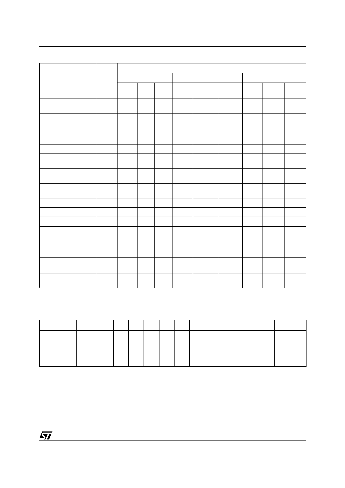
Table 6. DC Characteristics
Symbol Parameter Device Test Condition Min Typ Max Unit
I
LI
Input Leakage Current Flash & SRAM
0V≤ V
IN
≤
V
DDQF
±1 µA
I
LO
Output Leakage Current
Flash
0V ≤V
OUT
≤
V
DDQF
±10 µA
SRAM
0V ≤V
OUT
≤
V
DDQF,
SRAM Outputs Hi-Z
±1 µA
I
DDSVDD
Standby Current
Flash
E
F
= V
DDQF
± 0.2V
RP
F
= V
DDQ
± 0.2V
15 50 µA
SRAM
E1
S
≥
V
DDS
– 0.2V
V
IN
≥
V
DDS
−
0.2V or V
IN
≤
0.2V
515µA
I
DDD
Supply Current (Reset) Flash
RP
F
= V
SSF
± 0.2V
15 50 µA
I
DD
Supply Current SRAM
V
DDS
= 3.3V
,
I
OUT
= 0 mA, f = 1MHz
1.5 3 mA
V
DDS
= 3.3V
,
I
OUT
= 0 mA, f = f
MAX
= 1/t
AVAV
715mA
I
DDR
Supply Current (Read) Flash
E
F
= VIL, G
F
=
V
IH,
f = 5 MHz
10 20 mA
I
DDW
Supply Current
(Program)
Flash
Program in progress
V
PPF
= 12V ± 5%
10 20 mA
Program in progress
V
PPF
= V
DDF
10 20 mA
I
DDE
Supply Current (Erase) Flash
Erase in progress
V
PPF
= 12V ± 5%
520mA
Erase in progress
V
PPF
= V
DDF
520mA
I
DDES
Supply Current
(Program/Erase
Suspend)
Flash
E
F
= V
DDQF
± 0.2V,
Erase suspended
50 µA
I
PP1
Program Current
(Read or Standby)
Flash
V
PPF
> V
DDF
400 µA
I
PP2
Program Current
(Read or Standby)
Flash
V
PPF
≤
V
DDF
5µA
I
PPR
Program Current (Reset) Flash
RP
F
= V
SSF
± 0.2V
5µA
I
PPW
Program Current
(Program)
Flash
V
PPF
= 12V ± 0.5V
Program in progress
10 mA
V
PPF
= V
DDF
Program in progress
5mA
I
PPE
Program Current (Erase) Flash
V
PPF
= 12V ± 0.5V
Erase in progress
10 mA
V
PPF
= V
DDF
Erase in progress
5µA
V
IL
Input Low Voltage Flash & SRAM
V
DDQF
= V
DDS
≥
2.7V
–0.3 0.6 V
V
IH
Input High Voltage Flash & SRAM
V
DDQF
= V
DDS
≥
2.7V 0.7V
DDQF
V
DDQF
+0.3
V
Page 14
M36W216TI, M36W216BI
14/62
V
OL
Output Low Voltage Flash & SRAM
V
DDQF
= V
DDS
= VDDmin
I
OL
= 100µA
0.1 V
V
OH
Output High Voltage Flash & SRAM
V
DDQF
= V
DDS
= VDDmin
I
OH
= –100µA
V
DDQ
–0.1
V
V
PP1
Program Voltage
(Program or Erase
operations)
Flash 1.65 3.6 V
V
PPFH
Program Voltage
(Program or Erase
operations)
Flash 11.4 12.6 V
V
PPLK
Program Voltage
(Program and Erase
lock-out)
Flash 1 V
V
LKO
V
DDF
Supply Voltage
(Program and Erase
lock-out)
Flash 2 V
Symbol Parameter Device Test Condition Min Typ Max Unit
Page 15
15/62
M36W216TI, M36W216BI
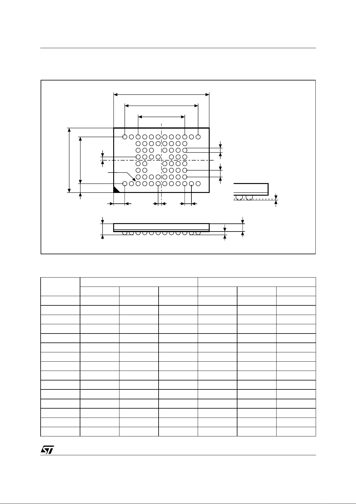
PACKAGE MECHANICAL
Figure 7. Stacked LFBGA66-12x8mm, 8x8 ball arra y, 0.8mm pitch, Bottom View Package Outline
Note: Drawing is not to scale.
Table 7. Stacked LFBGA66 - 12x8mm, 8x8 ball array, 0.8 mm pitch, Pack age Mechanical Data
Symbol
millimeters inches
Typ Min Max Typ Min Max
A 1.400 0.0551
A1 0.300 0.0118
A2 1.100 0.0433
b 0.400 0.300 0.500 0.0157 0.0118 0.0197
D 12.000 – – 0.47 24 – –
D1 5.600 – – 0.22 05 – –
D2 8.800 – – 0.34 65 – –
ddd 0.100 0.0039
E 8.000 – – 0.31 50 – –
E1 5.600 – – 0.2205 – –
e 0.800 – – 0.03 15 – –
FD 1.600 – – 0.0630 – –
FE 1.200 – – 0.04 72 – –
SD 0 .400 – – 0.0157 – –
SE 0.400 – – 0.0157 – –
A2
A1
A
BGA-Z12
ddd
D
E
e
b
SE
FDFE
E1
e
D1
SD
D2
BALL "A1"
Page 16
M36W216TI, M36W216BI
16/62
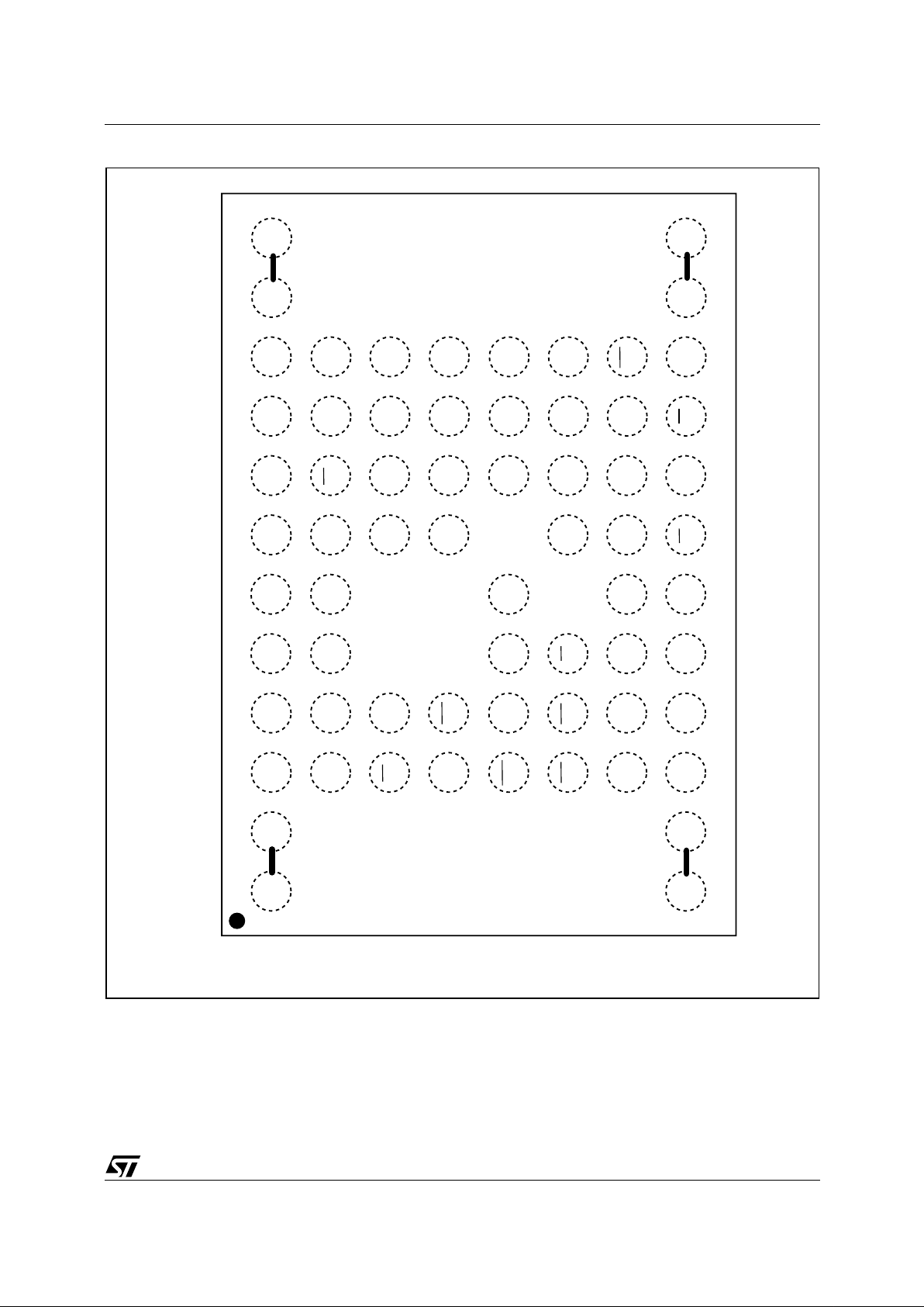
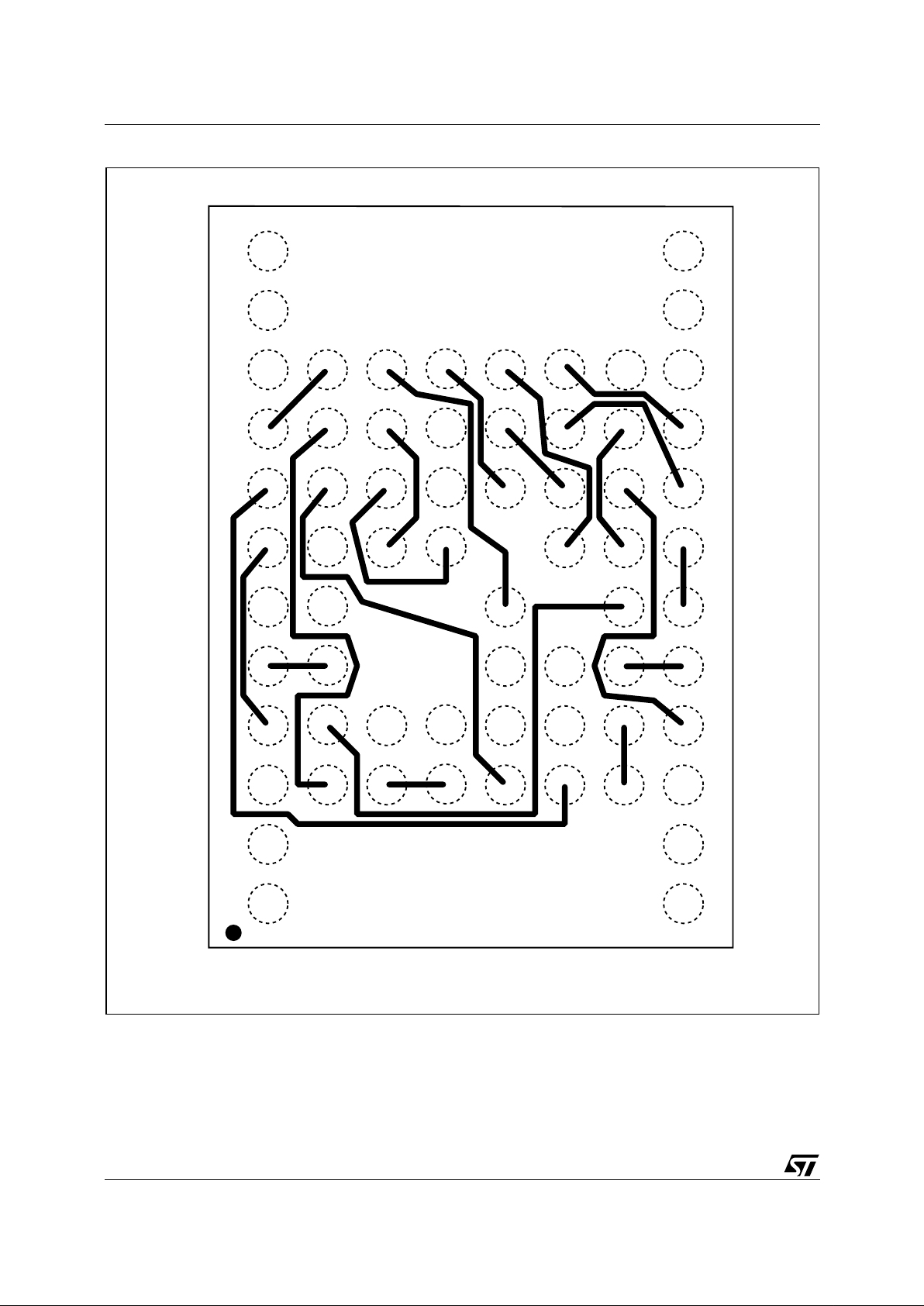
Figure 8. Stacked LFBGA66 Daisy Chain - Package Connections (Top view through package)
AI90273
D
C
#4#3
8761
E
F
A
B
H
G
5
4
32#1 #2
Page 17
17/62
M36W216TI, M36W216BI
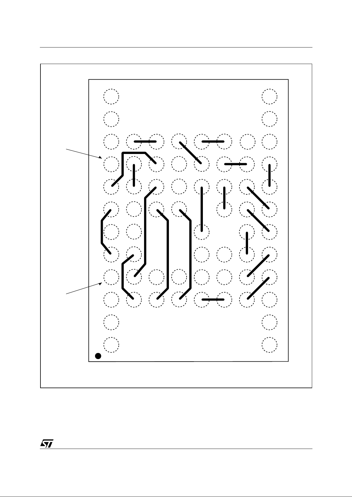
Figure 9. Stacked LFBGA66 Daisy Chain - PCB Connections proposal (Top view through package)
#1
AI90274
D
C
E
F
A
B
H
G
START
POINT
END
POINT
#4#3
87615
4
32#2
Page 18

M36W216TI, M36W216BI
18/62
PART NUMBERING
Table 8. Ordering Information Scheme
Devices are shipped from the factory with the memory content bits erased to ’1’.
Table 9. Daisy Chain Ordering Scheme
For a list of available options (Speed, Package, etc.) or for further information on any aspect of this device,
please contact the STMicroelectronics Sales Office nearest to you.
Example: M36W216 T I 85 ZA 6 T
Device Type
M36 = MMP (Flash + SRAM)
Operating Voltage
W = V
DDF
= 2.7V to 3.3V, V
DDS
= V
DDQF
= 2.7V to 3.3V
SRAM Chip Size & Organization
2 = 2 Mbit (128K x 16 bit)
Device Function
16 = 16 Mbit (x16), Boot Block
Array Matrix
T = Top Boot
B = Bottom Boot
SRAM Component
I = 2Mb, 0.16µm, 70ns, 3V
Speed
70 = 70ns
85 = 85ns
Package
ZA = LFBGA66: 12x8mm, 0.8mm pitch
Temperature Range
1 = 0 to 70°C
6 = –40 to 85°C
Option
T = Tape & Reel packing
Example: M36W216TI -ZA T
Device Type
M36W216TI
Daisy Chain
-ZA = LFBGA66: 0.8mm pitch
Option
T = Tape & Reel Packing
Page 19

19/62
M36W216TI, M36W216BI
FLASH DEVICE
The M36W216TI contains one 16 Mbit Flash
memory. This section describes how to use the
Flash device and all signals refer to the Flash device .
FLASH SUMMARY DESCRIPTION
The Flash Memory is a 16 Mb it (1 Mb it x 16) nonvolatile device that can be erased electrically at
the block level and prog rammed in-system on a
Word-by-Word basis. These operations can be
performed using a single low voltage (2.7 to 3.6V)
supply. V
DDQF
is used to drive the I/O pin down to
1.65V. An optional 12V V
PPF
power supply is pro-
vided to speed up customer programming.
The device features an asymmetrical blocked ar-
chitecture with an array of 39 blocks: 8 Parameter
Blocks of 4 KWords and 31 Main Blocks of 32
KWords. The M36W216TI has the Parameter
Blocks at the top of the memory address space
while the M36W216BI locates the Parameter
Blocks starting from the bottom. The memory
maps are shown in Figure 10, Block Addresses.
The Flash Memory features an instant, individual
block locking scheme that allows any block to be
locked or unlocked with no latency, enabling instant code and data protection. All blocks have
three levels of protection. They can be locked and
locked-down individually preventing any accidental programming or erasure. There is an additional
hardware protection against program and erase.
When V
PPF
≤ V
PPLK
all blocks are protected
against program or erase. All blocks are locked at
Power Up.
Each block can be erased separately. Erase can
be suspended in order to perform either read or
program in any other block and then resumed.
Program can be suspended to read data in any
other block and then resumed. Each block can be
programmed and erased over 100,000 cycles.
The device includes a 128 b it Protection Register
and a Security Block to increase the protection of
a system design. The Protection Register is divided into two 64 bit segments, the first one contains
a unique device number written by ST, while the
second one is one-time-programmable by the user. The user programmable segm ent can be permanently protected. The Security Block,
parameter block 0, can be permanentl y protected
by the user. Figure 11, shows the Flash Security
Block Memory Map.
Program and Erase command s are written to the
Command Interface of the memory. An on-chip
Program/Erase Controller takes care of the timings necessary for program and erase operations.
The end of a program or erase operation can be
detected and any error conditions identified. The
command set required to control the memory is
consistent with JEDEC standards.
Page 20

M36W216TI, M36W216BI
20/62
Figure 10. Flash Block Addresses
Note: Also see Appendix A, Tables 25 and 26 f or a full listing of the Flash Bl ock Addresses.
Figure 11. Flash Security Block and Protection Register Memory Map
AI90256
4 KWords
FFFFF
FF000
32 KWords
0FFFF
08000
32 KWords
07FFF
00000
Top Boot Block Addresses
4 KWords
F8FFF
F8000
32 KWords
F0000
F7FFF
Total of 8
4 KWord Blocks
Total of 31
32 KWord Blocks
4 KWords
FFFFF
F8000
32 KWords
32 KWords
00FFF
00000
Bottom Boot Block Addresses
4 KWords
F7FFF
0FFFF
32 KWords
F0000
08000
Total of 31
32 KWord Blocks
Total of 8
4 KWord Blocks
07FFF
07000
AI07905
Parameter Block # 0
User Programmable OTP
Unique device number
Protection Register Lock 2 1 0
88h
85h
84h
81h
80h
SECURITY BLOCK
PROTECTION REGISTER
Page 21

21/62
M36W216TI, M36W216BI
FLASH BUS OPERATIONS
There are six standard bus operations that control
the device. These are Bus Read, Bus Wri te, Output Disable, Standby, Automatic Standby and Reset. See Table 2, Main Operation Modes, for a
summary.
Typically glitches of less than 5ns on Chip Enable
or Write Enable are ignored by the memory and do
not affect bus operations.
Read. Read Bus operations are used to output
the contents of the Memory Array, the Electronic
Signature, the Status Register and the Common
Flash Interface. Both Chip Enable and Output Enable must be at V
IL
in order to perform a read operation. The Chip Enable input should be used t o
enable the device. Out put E nable shoul d be used
to gate data onto th e output. The data read depends on the previous command written to the
memory (see Command Interface section). See
Figure 12, Flash Read Mode AC W av eforms , and
Table 18, Flash Read AC Chara cteristics, for details of when the output becomes valid.
Read mode is the default state of the device when
exiting Reset or after power-up.
Write. Bus Write operations write Comm ands to
the memory or latch Input Data to be programmed.
A write operation is initiated when Chip Enable
and Write Enable are at V
IL
with Output Enable at
V
IH
. Commands, Input Data and Addresses are
latched on the rising edge of Write Enable or Chip
Enable, whichever occurs first.
See Figures 13 and 14, Flash Write AC Waveforms, and Tables 19 and 20, Flash Write AC
Characteristics, for details of the timing requirements.
Output Disa bl e . The data outputs are high impedance when the Output Enable is at V
IH
.
Standby. Stan dby disables most of the inte rnal
circuitry allowing a substantial reduction of the current consumption. The memory is in stand-by
when Chip Enable is at V
IH
and the device is in
read mode. The power consumption is reduced to
the stand-by level and the o utputs are set to high
impedance, independently from the Output Enable
or Write Enable inputs. If Chip Enable switches to
V
IH
during a program or erase operation, t he de-
vice enters Standby mode when finished.
Automatic Standby. Automatic Standby pro-
vides a low power consumption state during Read
mode. Following a read operation, the device enters Automatic Standby after 150ns of bus inactivity even if Chip Enable is Low, V
IL
, and the supply
current is reduced to I
DD1
. The data I nputs/Outputs will still output data if a bus Read operation is
in progress.
Reset. During Reset mode when Output Enable
is Low, V
IL
, the memory is deselected and the outputs are high impedance. The memory is in Reset
mode when Reset is at V
IL
. The power consumption is reduced to the Standby level, independently
from the Chip Enable, Output Enable or Write Enable inputs. If Reset is pulled to V
SS
during a Program or Erase, this operation is aborted and the
memory content is no longer valid.
Page 22

M36W216TI, M36W216BI
22/62
FLASH COMMAND INTERFACE
All Bus Write operations t o the me mory are in terpreted by the Command Interface. Commands
consist of one or more sequential Bus Write operations. An internal Program/Erase Controller handles all timings and verifies the correct execution
of the Program and Erase commands. The Program/Erase Controller provides a Status Regi ster
whose output may be read at any time during, to
monitor the progress of the operat ion, or the Program/Erase states. See Appendix 29, Table 33,
Write State Machine Current/Next, for a summary
of the Command Interface.
The Command Interface is reset to Read mode
when power is first applied, when exiting from Reset or whenever V
DD
is lower than V
LKO
. Command sequences must be followed exactly. Any
invalid combination of commands will reset the device to Read mode. Refer to Table 10, Commands, in conjunction with the text descriptions
below.
Read Memory Array Command
The Read command returns the memory to its
Read mode. One Bus Write cycle is required to issue the Read Memory Array command and return
the memory to Read mode. Subsequ ent read operations will read the addressed location and output the data. When a device Reset occurs, the
memory defaults to Read mode.
Read Status Register Command
The Status Register indicates when a program or
erase operation is complete and the success or
failure of the operation itself. Issue a Read Status
Register command to rea d the Status Register’s
contents. Subsequent Bus Read op erations read
the Status Register at any address, u ntil another
command is issued. See Table 17, Status Register
Bits, for details on the definitions of the bits.
The Read Status Register command m ay be issued at any time, even during a Program/Erase
operation. Any Read attempt during a Program/
Erase operation will automatically output the content of the Status Register.
Read Electronic Signature Command
The Read Electronic Signature command reads
the Manufacturer and Device Codes and the Block
Locking Status, or the Protection Register.
The Read Electronic Signature command consists
of one write cycle, a subsequent read will ou tput
the Manufacturer Code, the Device Code, the
Block Lock and Lock-Down Status, or the Protection and Lock Register. See Tables 11, 12 and 13
for the valid address.
Read CFI Query Command
The Read Query Command is used to read dat a
from the Common Flash Interface (CFI) Memory
Area, allowing programming equi pment or applications to automatically match their interface to
the characteristics of the device. One Bus Write
cycle is required to issue the Read Query Command. Once the command is issued subsequent
Bus Read operations read from the Common
Flash Interface Memory Area. See Appendix B,
Common Flash Inte rface, Tables 27, 28, 29, 30,
31 and 32 for details on the information contained
in the Common Flash Interface memory area.
Block Erase Command
The Block Erase com mand can be used to erase
a block. It sets all the bits within the selected block
to ’1’. A ll previous data in t he block is lost. If the
block is protected then the Erase operation will
abort, the data in the block will not be changed and
the Status Register will output the error.
Two Bus Write cycles are required to issue the
command.
■ The first bus cycle sets up the Erase command.
■ The second latches the block address in the
internal state machine and starts the Program/
Erase Controller.
If the second bus cycle is not Write Erase Confirm
(D0h), Status Register bits b4 and b5 are set and
the command aborts.
Erase aborts if Reset turns to V
IL
. As data integrity
cannot be guaranteed when the Erase operation is
aborted, the block must be erased again.
During Erase operations the memory will accept
the Read Status Re gister com mand and the P rogram/Erase Suspend command, all other commands will be ignored. Typical Erase times are
given in Table 14, Program, Erase Times and Program/Erase Endurance Cycles.
See Appendix C, Figure 28 , Erase Flowchart and
Pseudo Code, for a suggested flowchart for us ing
the Erase command.
Program Command
The memory array can be programmed word-byword. Two bus write cycles are required to issue
the Program Command.
■ The first bus cycle sets up the Program
command.
■ The second latches the Address and the Data to
be written and starts the Program/Erase
Controller.
During Program operations the memory will accept the Read Status Register command and the
Program/Erase Suspend command. Typical Program times are given in Table 14, Program, Erase
Times and Program/Erase Endurance Cycles.
Programming aborts if Reset goe s to V
IL
. As data
integrity cannot be guaranteed when the program
Page 23

23/62
M36W216TI, M36W216BI
operation is aborted, the block containing the
memory location must be erased and reprogrammed.
See Appendix C, Figure 25, Program Flowchart
and Pseudo Code, for the f lowchart for using the
Program command.
Double Word Program Command
This feature is offered to improve the programming
throughput, writing a page of two adjacent words
in parallel.The two words m ust differ only for the
address A0. Programm ing s hould not b e at t emp ted when V
PP
is not at V
PPFH
. The command can
be executed if V
PP
is below V
PPFH
but the result is
not guaranteed.
Three bus write cycles are necessary to issue the
Double Word Program command.
■ The first bus cycle sets up the Double Word
Program Command.
■ The second bus cycle latches the Address and
the Data of the first word to be written.
■ The third bus cycle latches the Address and the
Data of the second word to be written and starts
the Program/Erase Controller.
Read operations output the Status Register content after the programming has s tarted. Programming aborts if Res et goes to V
IL
. As data integrity
cannot be guaranteed when the program operation is aborted, the block containing the memory
location must be erased and reprogrammed.
See Appendix C, Figure 26, Double Word Program Flowchart and Pseudo Code, for the flowchart for using the Double Word Program
command.
Clear Status Register Command
The Clear Status Register comm and can be used
to reset bits 1, 3, 4 and 5 in the Status Register to
‘0’. One bus write cycle is required to issue the
Clear Status Register command.
The bits in the Status Register do not automatically return to ‘0’ when a new Program or Erase command is issued. The error bits in the Status
Register should be cleared before attempting a
new Program or Erase command.
Program/Erase Suspend Command
The Program/Erase Suspend command is used to
pause a Program or Erase operation. One bus
write cycle is required to issue the Program/Erase
command and pau se the Prog ram/Erase controller.
During Program/Erase Suspend the Command Interface will accept the Program/Erase Resume,
Read Array, Read Status Register, Read Electronic Signature and Read CFI Query commands. Additionally, if the suspend operation was Erase then
the Program, Block Lock, Block Lock-Down or
Protection Program commands will also be accepted. The block being erased may be protected
by issuing the Block Protect, Block Lock or Protection Program commands. When the Program/
Erase Resume comm and is issued the operation
will complete. Only the blocks not being erased
may be read or programmed correctly.
During a Program/Erase Suspend, the device can
be placed in a pseudo-standby mode by taking
Chip Ena ble to V
IH
. Program/Erase is aborted if
Reset turns to V
IL
.
See Appendix C, Figure 27 , Program Suspend &
Resume Flowchart and Pseudo Code, and Figure
29, Erase Suspend & Resume Flowchart and
Pseudo Code for flowcharts for using the Program/
Erase Suspend command.
Program/Er ase Resume Command
The Program/Erase Resume command can be
used to restart the Program/Erase Controller after
a Program/Erase Suspend operation has paused
it. One Bus Write cycle is required to issue the
command. Once the command is issued subsequent Bus Read operations read the Status Register.
See Appendix C, Figure 27 , Program Suspend &
Resume Flowchart and Pseudo Code, and Figure
29, Erase Suspend & Resume Flowchart and
Pseudo Code for flowcharts for using the Program/
Erase Resume command.
Prot e ction R e gister P rogram C om m and
The Protection Register Program command is
used to Program the 64 bit user One-Time-Programmable (OTP) segment of the Protection Register. The segment is programmed 16 bits at a
time. When shipped all bits in the segment are set
to ‘1’. The user can only program the bits to ‘0’.
Two write cycles are required to issue the Protection Register Program command.
■ The first bus cycle sets up the Protection
Register Program command.
■ The second latches the Address and the Data to
be written to the Protection Register and starts
the Program/Erase Controller.
Read operations output the Status Register content after the programming has started.
The segment can be protected by programming bit
1 of the Protection Lock Register. Bit 1 of the Protection Lock Register prote cts bit 2 of the P rotection Lock Register. Programming bit 2 of the
Protection Lock Register will result in a permanent
protection of the Security Block (see Figure 11,
Flash Security Block and Protection Register
Memory Map). Attempting to program a previously
protected Protection Register will result in a Status
Register error. The protection of the Protection
Page 24

M36W216TI, M36W216BI
24/62
Register and/or the Security Block is not reversible.
The Protection Register Program cannot be suspended. See Appendix C, Figure 31, Protection
Register Program Flowchart and Pseudo Code,
for the flowchart for using the P rotection Register
Program command.
Block Lock Command
The Block Lock command is used to lock a block
and prevent Program or Erase operations from
changing the data in it. All blocks are locked at
power-up or reset.
Two Bus Write cycles are required to issue the
Block Lock command.
■ The first bus cycle sets up the Block Lock
command.
■ The second Bus Write cycle latc hes the blo ck
address.
The lock status can be monitored for each block
using the Read Electronic Signature command.
Table. 16 shows the protection status after issuing
a Block Lock command.
The Block Lock bits are volatile, once set they remain set until a hardware reset or power-down/
power-up. They are cleared by a Blocks Unlock
command. Refer to the section, Block Locking, for
a detailed explanation.
Block Unlock Command
The Blocks Unlock command i s used to unlock a
block, allowing the block to be programmed or
erased. Two Bus Write cycles are requ ired to issue the Blocks Unlock command.
■ The first bus cycle sets up the Block Unlock
command.
■ The second Bus Write cycle latc hes the blo ck
address.
The lock status can be monitored for each block
using the Read Electronic Signature command.
Table. 16 shows the protection status after issuing
a Block Unlock command. Refer to the section,
Block Locking, for a detailed explanation.
Block Lock-Down Command
A locked block cannot be Programmed or Erased,
or have its protection status changed when WP
F
is
low, V
IL
. Whe n WPF is high, V
IH,
the Lock-Down
function is disabled and the lock ed blocks can be
individually unlocked by the Block Unlock command.
Two Bus Write cycles are required to issue the
Block Lock-Down command.
■ The first bus cycle sets up the Block Lock
command.
■ The second Bus Write cycle latc hes the blo ck
address.
The lock status can be monitored for each block
using the Read Electronic Signature command.
Locked-Down blocks revert to the locked (and not
locked-down) state when the device is reset on
power-down. Table. 16 sho ws the protection status after issuing a Block Lock-Down command.
Refer to the section, Block Locking, for a detailed
explanation.
Page 25
25/62
M36W216TI, M36W216BI
Table 10. Flash Commands
Note: 1. X = Don’t Care.
2. The s i gnature addresses are li st e d in Tables 11, 12 and 13.
3. Addr 1 and Addr 2 must be consecutive Addresses differing only for A0.
Table 11. Read Electronic Signature
Note: RPF = VIH.
Commands
No. of
Cycles
Bus Write Operations
1st Cycle 2nd Cycle 3nd Cycle
Bus
Op.
Addr Data
Bus
Op.
Addr Data
Bus
Op.
Addr Data
Read Memory Array 1+ Write X FFh
Read
Read
Addr
Data
Read Status Regist er 1+ Write X 70h
Read
X
Status
Register
Read Electro nic Signature 1+ Write X 90h
Read
Signature
Addr
(2)
Signature
Read CFI Query 1+ Write X 98h Read CFI Addr Query
Erase 2 Write X 20h Write
Block
Addr
D0h
Program 2 Write X
40h or
10h
Write Addr
Data
Input
Double Word Program
(3)
3 Write X 30h Write Addr 1
Data
Input
Write Addr 2
Data
Input
Clear Status Register 1 Write X 50h
Program/Erase Suspend 1 Write X B0h
Program/Erase Resume 1 Write X D0h
Block Loc k 2 Write X 60h Write
Block
Address
01h
Block Unlock 2 Write X 60h Write
Block
Address
D0h
Block Loc k-Down 2 Write X 60h Write
Block
Address
2Fh
Protection Register
Program
2 Write X C0h Write
Address
Data
Input
Code Device
E
F
GFW
F
A0 A1 A2-A7 A8-A19 DQ0-DQ7 DQ8-DQ15
Manufacture.
Code
V
IL
VILV
IH
V
ILVIL
0 Don’t Care 20h 00h
Device Code
M36W216TI
V
IL
VILV
IHVIHVIL
0 Don’t Care CEh 88h
M36W216BI
V
IL
VILV
IHVIHVIL
0 Don’t Care CFh 88h
Page 26

M36W216TI, M36W216BI
26/62
Table 12. Read Block Lock Signature
Note: 1. A Locked-Down Blo ck can be locked "D Q0 = 1" or unlocked "DQ0 = 0"; see Block Locking sec tion.
Table 13. Read Protection Register and Lock Register
Table 14. Program, Erase Times and Program /Eras e Endur ance Cycles
Block Status
E
F
GFW
F
A0 A1 A2-A7 A8-A11 A12-A19 DQ0 DQ1 DQ2-DQ15
Locked Block
V
ILVILVIHVILVIH
0 Don’t Care Block Address 1 0 00h
Unlocked Block
V
ILVILVIHVILVIH
0 Don’t Care Block Address 0 0 00h
Locked-Down
Block
V
ILVILVIHVILVIH
0 Don’t Care Block Address
X
(1)
1 00h
Word
E
F
GFW
F
A0-A7 A8-A19 DQ0 DQ1 DQ2 DQ3-DQ7 DQ8-DQ15
Lock
V
ILVILVIH
80h Don’t Care 0
OTP Prot.
data
Security
prot. data
00h 00h
Unique ID 0
V
ILVILVIH
81h Don’t Care ID data ID data ID data ID data ID data
Unique ID 1
V
ILVILVIH
82h Don’t Care ID data ID data ID data ID data ID data
Unique ID 2
V
ILVILVIH
83h Don’t Care ID data ID data ID data ID data ID data
Unique ID 3
V
ILVILVIH
84h Don’t Care ID data ID data ID data ID data ID data
OTP 0
V
ILVILVIH
85h Don’t Care OTP data OTP data OTP data OTP data OTP data
OTP 1
V
ILVILVIH
86h Don’t Care OTP data OTP data OTP data OTP data OTP data
OTP 2
V
ILVILVIH
87h Don’t Care OTP data OTP data OTP data OTP data OTP data
OTP 3
V
ILVILVIH
88h Don’t Care OTP data OTP data OTP data OTP data OTP data
Parameter Test Conditions
M36W216TI
Unit
Min Typ Max
Word Program
V
PP
= V
DD
10 200 µs
Double Word Program
V
PP
= 12V ±5%
10 200 µs
Main Block Program
V
PP
= 12V ±5%
0.16 5 s
V
PP
= V
DD
0.32 5 s
Parameter Block Program
V
PP
= 12V ±5%
0.02 4 s
V
PP
= V
DD
0.04 4 s
Main Block Erase
V
PP
= 12V ±5%
110 s
V
PP
= V
DD
110 s
Parameter Block Erase
V
PP
= 12V ±5%
0.8 10 s
V
PP
= V
DD
0.8 10 s
Program/Erase Cycles (per Block) 100,000 cycles
Page 27

27/62
M36W216TI, M36W216BI
FLASH BLOCK LOCKING
The Flash memory features an instant, individual
block locking scheme that allows any block to be
locked or unlocked with no latency. This locking
scheme has three levels of protection.
■ Lock/Unlock - this first level allows software-
only control of block locking.
■ Lock-Down - this second level requires
hardware interaction before locking can be
changed.
■ V
PP
≤ V
PPLK
- the third level offers a complete
hardware protection against program and erase
on all blocks.
The lock status of each block can be set to
Locked, Unlocked, and Lock-Down. Table 16, defines all of the possible protection states (WP
F
,
DQ1, DQ0), and Appendi x C, Figure 30, shows a
flowchart for the locking operations.
Reading a Block’s Lock Status
The lock status of every block can be read in the
Read Electronic Signature mode of the device. To
enter this mode write 90h t o the device. Subsequent reads at the a ddress s pecified in Table 12,
will output the lock status of that block. The lock
status is represented by DQ0 and DQ1. DQ0 indicates the Block Lock/Unlock status and is se t by
the Lock command and cleared by the Unlock
command. It is also automatically set when entering Lock-Down. DQ1 indicates the Lock-Down status and is set by the Lock-Down command. It
cannot be cleared by software, only by a hardware
reset or power-down.
The following sections explain the operation of the
locking system.
Locked State
The default status of all blocks on power-up or after a hardware reset is Locked (states (0,0,1) or
(1,0,1)). Locked blocks are fully protected from
any program or erase. Any program or erase operations attempted on a locked block will return an
error in the Status Register. The Status of a
Locked block can be changed to Unlocked or
Lock-Down using the appropriate software commands. An Unlocked block can be Locked by issuing the Lock command.
Unlocked State
Unlocked blocks (states (0,0,0), (1,0,0) (1,1,0)),
can be programmed or erased. All unlocked
blocks return to the Locked state a ft er a hardware
reset or when the device is powered-down. The
status of an unlocked block can be changed to
Locked or Locked-Down using the appropriate
software commands. A locked block can be unlocked by issuing the Unlock command.
Lock-Down State
Blocks that are Locked-Down (state (0,1,x))are
protected from program and erase operations (as
for Locked blocks) but their lock status cannot be
changed using software commands alone. A
Locked or Unlocked block can be Locked-Down by
issuing the Lock-Down com mand. Locked-Down
blocks revert to the Locked state when the device
is reset or powered-down.
The Lock-Down function is dependent on the WP
F
input pin. When WPF=0 (VIL), the blocks in the
Lock-Down state (0,1,x) are protected from program, erase and protection status changes. When
WP
F
=1 (VIH) the Lock-Down function is disabled
(1,1,1) and Locked-Down blocks can be ind ividually unlocked to the (1,1,0) state by issuing the
software command, where they can be erased and
programmed. These blocks can then be relocked
(1,1,1) and unlocked (1,1,0) as desired while WP
F
remains high. When WPF is low , blocks that were
previously Locked-Down return to the Lock-Down
state (0,1,x) regardless of any changes made
while WP
F
was high. Device reset or power-down
resets all blocks , including those in Lock-Down, to
the Locked state.
Locking Operations During Erase Suspend
Changes to block lock status can be performed
during an erase suspend by using the standard
locking command sequences to unlock, lock or
lock-down a block. This is useful in the case when
another block needs to be updated while an erase
operation is in progress.
To change block locking during an erase operation, first write the Erase Suspend command, then
check the status register until it indicates that the
erase operation has been suspended. Next write
the desired Lock com mand sequence to a block
and the protection status will be changed. After
completing any desired lock, read, or program operations, resume the erase operation with the
Erase Resume command.
If a block is locked or locked-down during an erase
suspend of the same block, the locking status bits
will be changed immediately , but when the eras e
is resumed, the erase operation will complete.
Locking operations cannot be performed du ring a
program suspend. Refer to Appendix D, Command Interface and Program/Erase Controller
State, for detailed information on which commands are valid during erase suspend.
Page 28

M36W216TI, M36W216BI
28/62
Table 15. Block Lock Status
Table 16. Protection Status
Note: 1. The p rotection st atus is de fined by th e write prot ect pin and by DQ1 (‘1’ for a l ocked-dow n block) and DQ0 (‘1’ for a locked block)
as read in the Read Electroni c Signatu re command with A1 = V
IH
and A0 = VIL.
2. All blocks are loc ked at power-up, so the default config uration is 00 1 or 101 accor di ng to WP
F
status.
3. A WP
F
transition to VIH on a locked block will restore the previous DQ0 value, giving a 111 or 110.
Item Address Data
Block Lock Configuration
xx002
LOCK
Block is Unlocked DQ0=0
Block is Locked DQ0=1
Block is Locked-Down DQ1=1
Current
Protection Status
(1)
(WPF, DQ1, DQ0)
Next Protection Status
(1)
(WPF, DQ1, DQ0)
Current State
Program/Erase
Allowed
After
Block Lock
Command
After
Block Unlock
Command
After Block
Lock-Down
Command
After
WP
F
transition
1,0,0 yes 1,0,1 1,0,0 1,1,1 0,0,0
1,0,1
(2)
no 1,0,1 1,0,0 1,1,1 0,0,1
1,1,0 yes 1,1,1 1,1,0 1,1,1 0,1,1
1,1,1 no 1,1,1 1,1,0 1,1,1 0,1,1
0,0,0 yes 0,0,1 0,0,0 0,1,1 1,0,0
0,0,1
(2)
no 0,0,1 0,0,0 0,1,1 1,0,1
0,1,1 no 0,1,1 0,1,1 0,1,1
1,1,1 or 1,1,0
(3)
Page 29

29/62
M36W216TI, M36W216BI
FLASH STATUS REGISTER
The Status Register provides information on t he
current or previous Program or Erase operation.
The various bits convey information and errors on
the operation. To read the Status register the
Read Status Register command can be issued, refer to Read Status Register Command section. To
output the contents, the Status Register is latched
on the falling edge of the Chip Enable or Output
Enable signals, and can be read until Chip Enable
or Output Enable returns to V
IH
. Either Chip Enable or Output Enable must be toggled to update
the latched data.
Bus Read operations from any address always
read the Status Register during Program and
Erase operations.
The bits in the Status Register are summarized in
Table 17, Status Register Bits. Refer to Table 17
in conjunction with the following text descriptions.
Program/Erase Controller Status (Bit 7). The Progra m/Erase Controller Status bit indicates whether
the Program/Erase Controller is active or inactive.
When the Program/Erase Controller Status bit is
Low (set to ‘0’), the Program/Erase Controller is
active; when the bit is High (set to ‘1’), the Program/Erase Controller is inactive, and the device
is ready to process a new command.
The Program/Erase Controller Status is Low immediately after a Program/Erase Suspend command is issued until the Program/Erase Controller
pauses. After the Program/Erase Controller pauses the bit is High .
During Program, Erase, operations the Program/
Erase Controller Status bit can be polled to find the
end of the operation. Other bits in the Status Register should not be tested until the Program/Erase
Controller completes the operation and the bit is
High.
After the Program/Erase Cont roller completes its
operation the Erase Status, Prog ram Status, V
PP
Status and Block Lock Status bits should be tested
for errors.
Erase Suspend Status (Bit 6). The Erase Suspend Status bit indicates that an Erase o peration
has been suspended or is going to be suspended.
When the Erase Suspend Status bit is High (set to
‘1’), a Program/Erase Suspend command has
been issued and the memory is waiting for a Program/Erase Resume command.
The Erase Suspend Status should only be considered valid when the Program/Erase Controller Status bit is High (Program/Erase Controller inactive).
Bit 7 is set within 30µs of the Program/Erase Suspend command being issued therefore the memory may still complete the operation rather than
entering the Suspend mode.
When a Program/Erase Re sume command is issued the Erase Suspend Status bit returns Low.
Erase Status (Bit 5). The Erase Status bit can be
used to identify if the memory has failed to verify
that the block has erased correctly. When the
Erase Status bit is High (set t o ‘1’), the Program/
Erase Controller has applied the max imum number of pulses to the block and still failed to verify
that the block has erased correctly. The Erase Status bit should be read once the Program/Erase
Controller Status bit is High (Program/Erase Controller inactive).
Once set High, the Erase Status bit can only be reset Low by a Clear Status Register command or a
hardware reset. If set High it should be reset before a new Program or Erase command is issued,
otherwise the new command will appear to fail.
Program Status (Bit 4). The Program Status bit
is used to identify a Program failure. When the
Program Status bit is High (set to ‘1’), the Program/Erase Controller has applied the maximum
number of pulses to the byte and still failed to verify that it has programmed correctly. The Program
Status bit should be read once the Program/Erase
Controller Status bit is High (Program/Erase Controller inactive).
Once set High, the Program Status bit can only be
reset Low by a Clear Status Register command or
a hardware reset. If set High it should be reset before a new command is issued, otherwise the new
command will appear to fail.
V
PP
Status (Bit 3). The VPP Status bit can be
used to identify an invalid volt age on the V
PP
pin
during Program and Erase operations. The V
PP
pin is only sampled at the beginning of a Program
or Erase operation. Indeterminate results can occur if V
PP
becomes invalid during an operation.
When the V
PP
Status bit is Low (set to ‘0’), the volt-
age on the V
PP
pin was sampled at a valid voltage;
when the V
PP
Status bit is High (set to ‘1’), the V
PP
pin has a voltage that is below the VPP Lockout
Voltage, V
PPLK
, the memory is protected and Pro-
gram and Erase operations cannot be performed.
Once set High, the V
PP
Status bit can only be reset
Low by a Clear Status Register command or a
hardware reset. If set High it should be reset before a new Program or Erase command is issued,
otherwise the new command will appear to fail.
Program Suspend Status (Bit 2). The Program
Suspend Status bit indicates that a Program operation has been suspended. When the Program
Suspend Status bit is High (set to ‘1’), a Program/
Erase Suspend command has been issued and
the memory is waiting for a Program/Erase Resume command. The Program Suspend Status
should only be considered valid when the Pro-
Page 30

M36W216TI, M36W216BI
30/62
gram/Erase Controller Status bit is High (Program/
Erase Controller inactive). Bit 2 is set wi thin 5µs of
the Program/Erase Suspend comm and being issued therefore the memory may still complete t he
operation rather than entering the Suspend mode.
When a Program/Erase Re sume command is issued the Program Suspend Status bit returns Low.
Block Protection Status (Bit 1). The Block Protection Status bit can be used to identify if a Program or Erase operation has tried to modify the
contents of a locked block.
When the Block Protection Status bit is High (set
to ‘1’), a Program or Erase operation has been attempted on a locked block.
Once set High, the Block Protection Status bit can
only be reset Low by a Clear Status Register command or a hardware reset. If set High it should be
reset before a new command is issued, otherwise
the new command will appear to fail.
Reserved (Bit 0). Bit 0 of the Status Register is
reserved. Its value must be masked.
Note: Refer to Appendix C, Flowcharts and
Pseudo Codes, for using the Status Register.
Table 17. Status Register Bits
Note: Logic level ’1’ is High, ’0’ is Low.
Bit Name Logic Level Definition
7 P/E.C. Status
’1’ Ready
’0’ Busy
6 Erase Suspend Status
’1’ Suspended
’0’ In progress or Completed
5 Erase Status
’1’ Erase Error
’0’ Erase Success
4 Program Status
’1’ Program Error
’0’ Program Success
3
V
PP
Status
’1’
V
PP
Invalid, Abort
’0’
V
PP
OK
2 Program Suspend Status
’1’ Suspended
’0’ In Progress or Completed
1 Block Protection Status
’1’ Program/Erase on protected Block, Abort
’0’ No operation to protected blocks
0 Reserved
Page 31

31/62
M36W216TI, M36W216BI
Figure 12. Flash Read Mode AC Waveforms
Table 18. Flash Read AC Characteristics
Note: 1. Sampled only, not 100% tested.
2. G
F
may be delayed by up to t
ELQV
- t
GLQV
after the falling edge of EF without increasing t
ELQV
.
Symbol Alt Parameter
Flash
Unit
70 85
t
AVAV
t
RC
Address Valid to Next Address Valid Min 70 85 ns
t
AVQV
t
ACC
Address Valid to Output Valid Max 70 85 ns
t
AXQX
(1)
t
OH
Address Transition to Output Transition Min 0 0 ns
t
EHQX
(1)
t
OH
Chip Enable High to Output Transition Min 0 0 ns
t
EHQZ
(1)
t
HZ
Chip Enable High to Output Hi-Z Max 20 20 ns
t
ELQV
(2)
t
CE
Chip Enable Low to Output Valid Max 70 85 ns
t
ELQX
(1)
t
LZ
Chip Enable Low to Output Transition Min 0 0 ns
t
GHQX
(1)
t
OH
Output Enable High to Output Transition Min 0 0 ns
t
GHQZ
(1)
t
DF
Output Enable High to Output Hi-Z Max 20 20 ns
t
GLQV
(2)
t
OE
Output Enable Low to Output Valid Max 20 20 ns
t
GLQX
(1)
t
OLZ
Output Enable Low to Output Transition Min 0 0 ns
DQ0-DQ15
AI07906
A0-A19
E
F
G
F
VALID
tAXQX
tAVAV
VALID
tAVQV
tELQV
tELQX
tGLQV
tGLQX
ADDR. VALID
CHIP ENABLE
OUTPUTS
ENABLED
DATA VALID STANDBY
tGHQX
tGHQZ
tEHQX
tEHQZ
Page 32

M36W216TI, M36W216BI
32/62
Figure 13. Flash Write AC Waveforms, Write Enable Contro lled
E
F
G
F
W
F
DQ0-DQ15
V
PPF
A0-A19
AI07907
WP
F
COMMAND CMD or DATA
STATUS REGISTER
VALID
tAVAV
tQVVPL
tAVWH
tWHAX
PROGRAM OR ERASE
tELWL tWHEH
tWHDXtDVWH
tWLWH
tWHWL
tVPHWH
SET-UP COMMAND CONFIRM COMMAND
OR DATA INPUT
STATUS REGISTER
READ
1st POLLING
tELQV
tWPHWH
tWHGL
tQVWPL
tWHEL
Page 33

33/62
M36W216TI, M36W216BI
Table 19. Flash Write AC Characteristics, Write Enable Controlled
Note: 1. Sampled only, not 100% tested.
2. Appl i cable if V
PPF
is seen as a logic input (V
PPF
< 3.6V).
Symbol Alt Parameter
Flash
Unit
70 85
t
AVAV
t
WC
Write Cycle Time Min 70 85 ns
t
AVWH
t
AS
Address Valid to Write Enable High Min 45 45 ns
t
DVWH
t
DS
Data Valid to Write Enable High Min 45 45 ns
t
ELWL
t
CS
Chip Enable Low to Write Enable Low Min 0 0 ns
t
ELQV
Chip Enable Low to Output Valid Min 70 85 ns
t
QVVPL
(1,2)
Output Valid to V
PPF
Low
Min 0 0 ns
t
QVWPL
Output Valid to Write Protect Low Min 0 0 ns
t
VPHWH
(1)
t
VPSVPPF
High to Write Enable High
Min 200 200 ns
t
WHAX
t
AH
Write Enable High to Address Transition Min 0 0 ns
t
WHDX
t
DH
Write Enable High to Data Transition Min 0 0 ns
t
WHEH
t
CH
Write Enable High to Chip Enable High Min 0 0 ns
t
WHEL
Write Enable High to Output Enable Low Min 25 25 ns
t
WHGL
Write Enable High to Output Enable Low Min 20 20 ns
t
WHWL
t
WPH
Write Enable High to Write Enable Low Min 25 25 ns
t
WLWH
t
WP
Write Enable Low to Write Enable High Min 45 45 ns
t
WPHWH
Write Protect High to Write Enable High Min 45 45 n s
Page 34

M36W216TI, M36W216BI
34/62
Figure 14. Flash Write AC Waveforms, Chip Enable Controlled
E
F
G
F
DQ0-DQ15
V
PPF
A0-A19
AI07908
W
F
WP
F
COMMAND
CMD or DATA STATUS REGISTER
VALID
tAVAV
tQVVPL
tAVEH
tEHAX
PROGRAM OR ERASE
tWLEL tEHWH
tEHDX
tDVEH
tELEH
tEHEL
tVPHEH
POWER-UP AND
SET-UP COMMAND
CONFIRM COMMAND
OR DATA INPUT
STATUS REGISTER
READ
1st POLLING
tELQV
tWPHEH
tEHGL
tQVWPL
Page 35

35/62
M36W216TI, M36W216BI
Table 20. Flash Write AC Characteristics, Chip Enable Controlled
Note: 1. Sampled only, not 100% tested.
2. Appl i cable if V
PPF
is seen as a logic input (V
PPF
< 3.6V).
Symbol Alt Parameter
Flash
Unit
70 85
t
AVAV
t
WC
Write Cycle Time Min 70 85 ns
t
AVEH
t
AS
Address Valid to Chip Enable High Min 45 45 ns
t
DVEH
t
DS
Data Valid to Chip Enable High Min 45 45 ns
t
EHAX
t
AH
Chip Enable High to Address Transition Min 0 0 ns
t
EHDX
t
DH
Chip Enable High to Data Transition Min 0 0 ns
t
EHEL
t
CPH
Chip Enable High to Chip Enable Low Min 25 25 ns
t
EHGL
Chip Enable High to Output Enable Low Min 25 25 ns
t
EHWH
t
WH
Chip Enable High to Write Enable High Min 0 0 ns
t
ELEH
t
CP
Chip Enable Low to Chip Enable High Min 45 45 ns
t
ELQV
Chip Enable Low to Output Valid Min 70 85 ns
t
QVVPL
(1,2)
Output Valid to V
PPF
Low
Min 0 0 ns
t
QVWPL
Data Valid to Write Protect Low Min 0 0 ns
t
VPHEH
(1)
t
VPSVPPF
High to Chip Enable High
Min 200 200 ns
t
WLEL
t
CS
Write Enable Low to Chip Enable Low Min 0 0 ns
t
WPHEH
Write Protect High to Chip Enable High Min 45 45 ns
Page 36
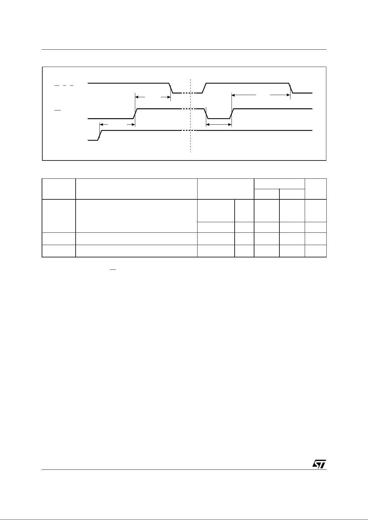
M36W216TI, M36W216BI
36/62
Figure 15. Flash Power-Up and Reset AC Waveforms
Table 21. Flash Power-Up and Reset AC Characteristics
Note: 1. The de vice Reset is possible but not guaranteed if t
PLPH
< 100ns.
2. Sampled only, not 100% tested.
3. It is im portant to ass ert RP
F
in order to allow proper CPU initialization during power up or reset.
Symbol Parameter Test Condition
Flash
Unit
70 85
t
PHWL
t
PHEL
t
PHGL
Reset High to Write Enable Low, Chip Enable
Low, Output Enable Low
During
Program and
Eras e
Min 50 50 µs
others Min 30 30 ns
t
PLPH
(1,2)
Reset Low to Reset High Min 100 100 ns
t
VDHPH
(3)
Supply Voltages High to Reset High Min 50 50 µs
AI07909b
WF,
RP
F
tPHWL
tPHEL
tPHGL
EF,G
F
V
DDF
, V
DDQF
tVDHPH
tPHWL
tPHEL
tPHGL
tPLPH
Power-Up Reset
Page 37

37/62
M36W216TI, M36W216BI
SRAM DEV ICE
This section describes ho w t o u se t he SRAM and
all signals refer to it.
SRAM SUMMARY DESCRIPTION
The SRAM is a 2 Mbit asynchronous random access memory which features super low voltage operation and low current consumption with an
access time of 70 ns under all conditions. The
memory operations can be performed using a single low voltage supply, 2.7V to 3.3V, which is the
same as the Flash component’s voltage supply.
Figure 16. SRAM Logic Diagram
DATA IN DRIVERS
128Kb x 16
RAM Array
2048 x 1024
COLUMN DECODER
ROW DECODER
A0-A10
W
S
UB
S
LB
S
SENSE AMPS
A11-A16
POWER-DOWN
CIRCUIT
E1
S
DQ0-DQ7
DQ8-DQ15
E2
S
G
S
UB
S
LB
S
AI
07910
Page 38

M36W216TI, M36W216BI
38/62
SRAM OPERATIONS
There are five standard operations that control the
SRAM component. These are Bus Read, Bus
Write, Standby/Power-down, Data Retention and
Output Disable. A summary is shown in Table 2,
Main Operation Modes
Read. Read operations are used to output the
contents of the SRAM Array. The SRAM is in Read
mode whenever Write Enable, W
S
, is a t VIH, Out-
put Enable, G
S
, is at VIL, Chip Enable , E1S, is at
V
IL
, Chip Enable, E2S, is at VIH, and one or both of
the Byte Enables, UB
S
and LBS is/are at VIL.
Valid data will be available on the output pins after
a time of t
AVQV
after the last stable address. If the
Chip Enable or Output Enable ac cess times are
not met, data access will be measured fro m the
limiting parameter (t
E1LQV
, t
E2HQV
, or t
GLQV
) rather than the address. Dat a out may be inde terminate at t
E1LQX
, t
E2HQX
and t
GLQX
, but data lines
will always be valid at t
AVQV
(see Table 22, Figures
17 and 18).
Write. Write operations are used to write da ta to
the SRAM. The SRAM is in Write mode whenever
W
S
and E1S are at VIL, and E2S is at VIH. Either
the Chip Enable inputs, E1
S
and E2S, or the Write
Enable input, W
S
, must be deasserted durin g ad-
dress transitions for subsequent write cycles.
A Write operation is initiated when E1
S
is at VIL,
E2
S
is at VIH and WS is at VIL. The data is latched
o the falling edge of E1
S
, the rising edge of E2S or
the falling edge of W
S
, whichever occurs last. The
Write cycle is terminated on the rising edge of E1
S
,
the rising edge of W
S
or the falling ed ge of E2S,
whichever occurs first.
If the Output is enabled (E1
S=VIL
, E2S=VIH and
G
S=VIL
), then WS will return the outputs to high im-
pedance within t
WLQZ
of its falling edge. Care must
be taken to avoid bus contention in this type of operation. The Data input must be valid for t
DVWH
be-
fore the rising edge of Write Enable, for t
DVE1H
before the rising edge of E 1S or for t
DVE2L
before
the falling edge of E2
S
, whichever occurs first, and
remain valid for t
WHDX
, t
E1HAX
or t
E2LAX
(see Table
23, Figures 20, 21, 22 and 23).
Standby/Power-Down. The SRAM component
has a chip enabled power-down feature wh ich invokes an automatic standby mode (see Table 22,
Figure 19). The SRAM is in Standby mode whenever either Chip Enable is deas serted, E1
S
at V
IH
or E2S at VIL. It is also possible when UBS and LB
S
are at VIH.
Data Retention. The SRAM data retention per-
formances as V
DDS
go down to VDR are described
in Table 24 and Figure 24. In E1
S
controlled data
retention mode, the minimum standby current
mode is entered when E1
S
≥ V
DDS
– 0.2V and
E2
S
≤ 0.2V or E2S≥ V
DDS
– 0.2V. In E2S controlled data retention mode, minimum standby current mode is entered when E2
S
≤ 0.2V.
Output Disa bl e . The data outputs are high impedance when the Output Enable, G
S
, is at V
IH
with Write Enable, WS, at VIH.
Page 39

39/62
M36W216TI, M36W216BI
Figure 17. SRAM Read Mode AC Waveforms, Address Controlled with UBS = LBS = V
IL
Note: E1S = Low, E2S = High, GS = Low, WS = High.
Figure 18. SRAM Read AC Waveforms, GS Controlled
Note: Write Enable (WS) = High. Address Valid prior to or at the same time as E1S, UBS and LBS going Low.
Figure 19. SRAM Standby AC Waveforms
AI07911
tAVAV
tAVQV
tAXQX
A0-A16
DQ0-DQ15
VALID
DATA VALIDDATA VALID
AI07912
tAVAV
tE1LQV tE1HQZ
tGLQV
tGLQX
tGHQZ
DATA VALID
A0-A16
E1
S
G
S
DQ0-DQ15
tE2HQV
VALID
tE2LQZ
E2
S
tBLQV
tBLQX
tBHQZ
UB
S
, LB
S
tE1LQX
tE2HQX
AI07913
tPD
E2
S
I
DD
tPU
50%
E1
S
Page 40
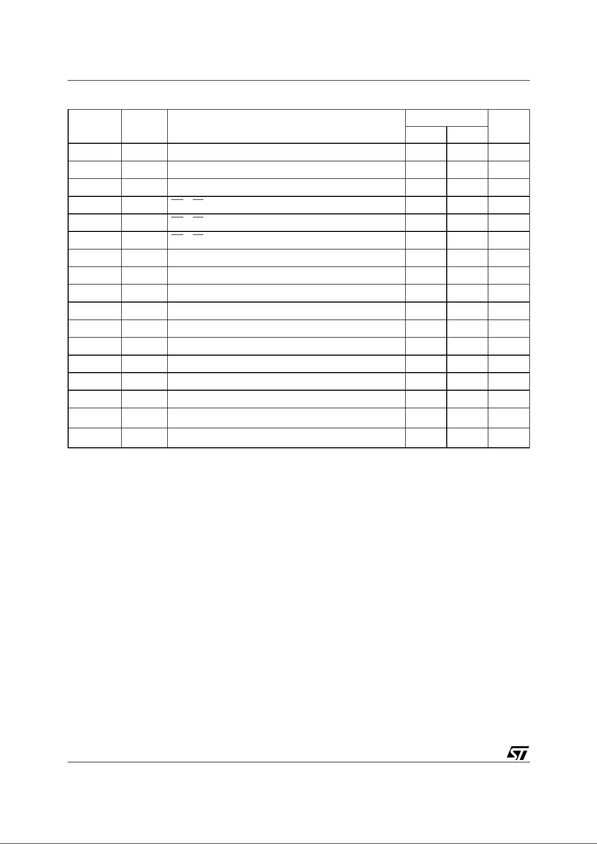
M36W216TI, M36W216BI
40/62
Table 22. SRAM Read AC Characteristics
Note: 1. Sampl e d only. Not 100% tested.
Symbol Alt Parameter
SRAM
Unit
Min Max
t
AVAV
t
RC
Read Cycle Time 70 ns
t
AVQV
t
ACC
Address Valid to Output Valid 70 ns
t
AXQX
t
OH
Address Transition to Output Transition 10 ns
t
BHQZ
t
BHZ
UBS, LBS Disable to Hi-Z Output
25 ns
t
BLQV
t
AB
UBS, LBS Access Time
70 ns
t
BLQX
t
BLZ
UBS, LBS Enable to Low-Z Output
5ns
t
E1HQZ
t
CHZ1
Chip Enable 1 High to Output Hi-Z 25 ns
t
E1LQV
t
ACS1
Chip Enable 1 Low to Output Valid 70 ns
t
E1LQX
t
CLZ1
Chip Enable 1 Low to Output Transition 10 ns
t
E2HQV
t
ACS2
Chip Enable 2 High to Output Valid 70 ns
t
E2HQX
t
CLZ2
Chip Enable 2 High to Output Transition 10 ns
t
E2LQZ
t
CHZ2
Chip Enable 2 Low to Output Hi-Z 25 ns
t
GHQZ
t
OHZ
Output Enable High to Output Hi-Z 25 ns
t
GLQV
t
OE
Output Enable Low to Output Valid 35 ns
t
GLQX
t
OLZ
Output Enable Low to Output Transition 5 ns
t
PD
(1)
Chip Enable 1 High or Chip Enable 2 Low to Power Down 70 ns
t
PU
(1)
Chip Enable 1 Low or Chip Enable 2 High to Power Up 0 ns
Page 41

41/62
M36W216TI, M36W216BI
Figure 20. SRAM Write AC Waveforms, WS Controlled
Note: WS, E1S, E2S, UBS and/or LBS must be asserted to initiate a write cycle. Ou tp ut Enable (GS) = Low (otherwis e , DQ0-DQ 15 are hig h
impedance). If E1
S
, E2S and WS are deasserted at the s ame time, DQ0-DQ15 remai n high impedance.
2. The I /O pins are in output mode and input signal s must not be applied.
AI07914
tAVAV
tWHAX
tDVWH
INPUT VALID
A0-A16
E1
S
W
S
DQ0-DQ15
VALID
E2
S
tAVWH
tBLWH
tGHQZ tWHDZ
tAVWL
UBS, LB
S
tE2HWH
tE1LWH
G
S
tWLWH
Note 2
Page 42

M36W216TI, M36W216BI
42/62
Figure 21. SRAM Write AC Waveforms, E1S Controlled
Note: 1. WS, E1S, E2S, UBS and/or LBS must be asserted to initiate a write cycle. Output Enable (GS) = Low (otherwise, DQ0-DQ15 are high
impedance). If E1
S
, E2S and WS are deasserted at the same time, DQ0-DQ15 remain high impedance.
2. If E1
S
, E2S and WS are deasserted at the sa m e time, DQ0-DQ15 remain high impe dance.
3. The I /O pins are in output mode and input signal s must not be applied.
AI07915
tAVAV
tE1HAX
tDVE1H
tDVE2L
INPUT VALID
A0-A16
E1
S
W
S
DQ0-DQ15
VALID
E2
S
tAVE1H
tAVE2L
tBLE1H
tBLE2L
tGHQZ
tE1HDZ
tE2LDZ
tAVE1L
UB
S
, LB
S
tE2HE2L
tE1LE1H
G
S
tWLE1H
tWLE2L
tAVE2H tE2LAX
Note 3
Page 43

43/62
M36W216TI, M36W216BI
Figure 22. SRAM Write AC Waveforms, WS Controlled with GS Low
Note: 1. If E1S, E2S and WS are deasserted at the sa m e time, DQ0-DQ15 remain high impe dance.
Figure 23. SRAM Write Cycle Waveform, UBS and LBS Controlled, GS Low
Note: 1. If E1S, E2S and WS are deasserted at the sa m e time, DQ0-DQ15 remain high impe dance.
AI07916
tAVAV
tWHAX
tDVWH
INPUT VALID
A0-A16
E1
S
W
S
DQ0-DQ15
VALID
E2
S
tAVWH
tWLWHtAVWL
tWHDZ
tWHQX
tBLWH
UB
S
, LB
S
tE1LWH
tE2HWH
tWLQZ
AI07917
tAVAV
tBHAX
tDVBH
INPUT VALID
A0-A16
E1
S
W
S
DQ0-DQ15
VALID
E2
S
tAVBH
tWLBH
tAVBL
tBHDZ
tBLBH
UB
S
, LB
S
tE1LBH
tE2HBH
Page 44

M36W216TI, M36W216BI
44/62
Table 23. SRAM Write AC Characteristics
Symbol Alt Parameter
SRAM
Unit
Min Max
t
AVAV
t
WC
Write Cycle Time 70 ns
t
AVE1L
,
t
AVE2H
,
t
AVWL
t
AS
Address Valid to Beginning of Write 0 ns
t
AVWH
t
AW
Address Valid to Write Enable High 60 ns
t
BLWH
t
BLE1H
t
BLE2L
t
AVBH
t
BW
UBS, LBS Valid to End of Write
60 ns
t
DVE1H
,
t
DVE2L
,
t
DVWH
t
DVBH
t
DW
Input Valid to End of Write 30 ns
t
E1HAX
,
t
E2LAX
,
t
WHAX
t
WR
End of Write to Address Change 0 ns
t
E1HDZ
,
t
E2LDZ
,
t
WHDZ
t
BHDZ
t
HD
Address Transition to End of Write 0 ns
t
E1LEIH
,
t
E1LWH
t
CW1
Chip Enable 1 Low to End of Write 60 ns
t
E2HE2L
t
E2HWH
t
CW2
Chip Enable 2 High to End of Write 60 ns
t
WHQX
t
DH
Write Enable High to Input Transition 10 ns
t
WLQZ
t
WHZ
Write Enable Low to Output Hi-Z 25 ns
t
WLWH
t
WLE1H
t
WLE2L
t
WP
Write Enable Pulse Width 45 ns
Page 45

45/62
M36W216TI, M36W216BI
Figure 24. SRAM Low V
DDS
Data Retention AC Waveforms, E1S or UBS / LBS Controlled
Table 24. SRAM Low V
DDS
Data Retention Characteristic
Note: 1 . All other Inputs V
IH
≤ V
DDS
–0.2V or V
IL
≤ 0.2V.
2. Sampled only. Not 100% tested.
Symbol Parameter Test Condition Min Typ Max Unit
I
DDDR
Supply Current (Data
Retention)
V
DDS
= 1.5V, E1
S
≥
V
DDS
– 0.2V,
V
IN
≥
V
DDS
– 0.2V or V
IN
≤
0.2V
310µA
V
DR
Supply Voltage (Data
Retention)
1.5 3.3 V
t
CDR
Chip Disable to Power Down
E1
S
≥
V
CCS
– 0.2V, E2
S
≤
0.2V
0ns
t
R
Operation Recovery Time 70 ns
AI07918
E1S or
UBS, LB
S
tCDR
V
DDS
tR
DATA RETENTION MODE
V
DDS (min)
V
DDS (min)
Page 46

M36W216TI, M36W216BI
46/62
APPENDIX A. BLOCK ADDRESS TABLES
Table 25. Top Boot Block Addresses,
M36W216TI
Table 26. Bottom Boot Block Addresses,
M36W216BI
#
Size
(KWord)
Address Range
0 4 FF000-FFFFF
1 4 FE000-FEFFF
2 4 FD000-FDFFF
3 4 FC000-FCFFF
4 4 FB000-FBFFF
5 4 FA000-FAFFF
6 4 F9000-F9FFF
7 4 F8000-F8FFF
8 32 F0000-F7FFF
99 32 E8000-EFFFF
10 32 E0000-E7FFF
11 32 D8000-DFFFF
12 32 D0000-D7FFF
13 32 C8000-CFFFF
14 32 C0000-C7FFF
15 32 B8000-BFFFF
16 32 B0000-B7FFF
17 32 A8000-AFFFF
18 32 A0000-A7FFF
19 32 98000-9FFFF
20 32 90000-97FFF
21 32 88000-8FFFF
22 32 80000-87FFF
23 32 78000-7FFFF
24 32 70000-77FFF
25 32 68000-6FFFF
26 32 60000-67FFF
27 32 58000-5FFFF
28 32 50000-57FFF
29 32 48000-4FFFF
30 32 40000-47FFF
31 32 38000-3FFFF
32 32 30000-37FFF
33 32 28000-2FFFF
34 32 20000-27FFF
35 32 18000-1FFFF
36 32 10000-17FFF
37 32 08000-0FFFF
38 32 00000-07FFF
#
Size
(KWord)
Address Range
38 32 F8000-FFFFF
37 32 F0000-F7FFF
36 32 E8000-EFFFF
35 32 E0000-E7FFF
34 32 D8000-DFFFF
33 32 D0000-D7FFF
32 32 C8000-CFFFF
31 32 C0000-C7FFF
30 32 B8000-BFFFF
29 32 B0000-B7FFF
28 32 A8000-AFFFF
27 32 A0000-A7FFF
26 32 98000-9FFFF
25 32 90000-97FFF
24 32 88000-8FFFF
23 32 80000-87FFF
22 32 78000-7FFFF
21 32 70000-77FFF
20 32 68000-6FFFF
19 32 60000-67FFF
18 32 58000-5FFFF
17 32 50000-57FFF
16 32 48000-4FFFF
15 32 40000-47FFF
14 32 38000-3FFFF
13 32 30000-37FFF
12 32 28000-2FFFF
11 32 20000-27FFF
10 32 18000-1FFFF
9 32 10000-17FFF
8 32 08000-0FFFF
7 4 07000-07FFF
6 4 06000-06FFF
5 4 05000-05FFF
4 4 04000-04FFF
3 4 03000-03FFF
2 4 02000-02FFF
1 4 01000-01FFF
0 4 00000-00FFF
Page 47

47/62
M36W216TI, M36W216BI
APPENDIX B. COMMON FLASH INTERFACE (CFI)
The Common Flash Interface is a JEDEC approved, standardized data structure that can be
read from the Flash memory device. It allows a
system software to query the device to det ermine
various electrical and t iming parameters, density
information and functions supported by the memory. The system can interface easily with the device, enabling the software to upgrade itself when
necessary.
When the CFI Query Co mmand (RCFI) is issued
the device enters CFI Query mode and the data
structure is read from the memory. Tables 27, 28,
29, 30, 31 and 32 show the addresses used to retrieve the data.
The CFI data structure also contains a security
area where a 64 bit unique security number is written (see Table 32, Security Code area). This area
can be accessed only in Read mode by the final
user. It is impossible to change the security num ber after it has been written by ST. Issue a Read
command to return to Read mode.
Table 27. Query Structure Overview
Note: Query data are always presented on the lowest order data outputs.
Table 28. CFI Query Identification String
Note: Query data are always presented on the lowest order data outputs (DQ7-DQ0) only. DQ8-DQ15 are ‘0’.
Offset Sub-section Name Description
00h Reserved Reserved for algorithm-specific information
10h CFI Query Identification String Command set ID and algorithm data offset
1Bh System Interface Information Device timing & voltage information
27h Device Geometry Definition Flash device layout
P Primary Algorithm-specific Extended Query table
Additional information specific to the Primary
Algorithm (optional)
A Alternate Algorithm-specific Extended Query table
Additional information specific to the Alternate
Algorithm (optional)
Offset Data Description Value
00h 0020h Manufacturer Code ST
01h
88CEh
88CFh
Device Code
Top
Bottom
02h-0Fh reserved Reserved
10h 0051h "Q"
11h 0052h Query Unique ASCII String "QRY" "R"
12h 0059h "Y"
13h 0003h
Primary Algorithm Command Set and Control Interface ID code 16 bit ID code
defining a specific algorithm
Intel
compatible
14h 0000h
15h 0035h
Address for Primary Algorithm extended Query table (see Table 30) P = 35h
16h 0000h
17h 0000h
Alternate Vendor Command Set and Control Interface ID Code second vendor specified algorithm supported (0000h means none exists)
NA
18h 0000h
19h 0000h
Address for Alternate Algorithm extended Query table
(0000h means none exists)
NA
1Ah 0000h
Page 48

M36W216TI, M36W216BI
48/62
Table 29. CFI Query System Interface Information
Offset Data Description Value
1Bh 0027h
V
DD
Logic Supply Minimum Program/Erase or Write voltage
bit 7 to 4 BCD value in volts
bit 3 to 0 BCD value in 100 mV
2.7V
1Ch 0036h
V
DD
Logic Supply Maximum Program/Erase or Write voltage
bit 7 to 4 BCD value in volts
bit 3 to 0 BCD value in 100 mV
3.6V
1Dh 00B4h
V
PP
[Programming] Supply Minimum Program/Erase voltage
bit 7 to 4 HEX value in volts
bit 3 to 0 BCD value in 100 mV
11.4V
1Eh 00C6h
V
PP
[Programming] Supply Maximum Program/Erase voltage
bit 7 to 4 HEX value in volts
bit 3 to 0 BCD value in 100 mV
12.6V
1Fh 0004h
Typical time-out per single word program = 2
n
µs
16µs
20h 0004h
Typical time-out for Double Word Program = 2
n
µs
16µs
21h 000Ah
Typical time-out per individual block erase = 2
n
ms
1s
22h 0000h
Typical time-out for full chip erase = 2
n
ms
NA
23h 0005h
Maximum time-out for word program = 2
n
times typical
512µs
24h 0005h
Maximum time-out for Double Word Program = 2
n
times typical
512µs
25h 0003h
Maximum time-out per individual block erase = 2
n
times typical
8s
26h 0000h
Maximum time-out for chip erase = 2
n
times typical
NA
Page 49

49/62
M36W216TI, M36W216BI
Table 30. Device Geometry Definition
Offset Word
Mode
Data Description Value
27h 0015h
Device Size = 2
n
in number of bytes
2 MByte
28h
29h
0001h
0000h
Flash Device Interface Code description
x16
Async.
2Ah
2Bh
0002h
0000h
Maximum number of bytes in multi-byte program or page = 2
n
4
2Ch 0002h
Number of Erase Block Regions within the device.
It specifies the number of regions within the device containing contiguous
Erase Blocks of the same size.
2
M36W216TI
2Dh
2Eh
001Eh
0000h
Region 1 Information
Number of identical-size erase block = 001Eh+1
31
2Fh
30h
0000h
0001h
Region 1 Information
Block size in Region 1 = 0100h * 256 byte
64 KByte
31h
32h
0007h
0000h
Region 2 Information
Number of identical-size erase block = 0007h+1
8
33h
34h
0020h
0000h
Region 2 Information
Block size in Region 2 = 0020h * 256 byte
8 KByte
M36W216BI
2Dh
2Eh
0007h
0000h
Region 1 Information
Number of identical-size erase block = 0007h+1
8
2Fh
30h
0020h
0000h
Region 1 Information
Block size in Region 1 = 0020h * 256 byte
8 KByte
31h
32h
001Eh
0000h
Region 2 Information
Number of identical-size erase block = 001Eh+1
31
33h
34h
0000h
0001h
Region 2 Information
Block size in Region 2 = 0100h * 256 byte
64 KByte
Page 50

M36W216TI, M36W216BI
50/62
Table 31. Primary Algorithm-Specific Extended Qu ery Ta bl e
Note: 1. See Table 28, offset 15 for P point er definitio n.
Offset
P = 35h
(1)
Data Description Value
(P+0)h = 35h 0050h
Primary Algorithm extended Query table unique ASCII string “PRI”
"P"
(P+1)h = 36h 0052h "R"
(P+2)h = 37h 0049h "I"
(P+3)h = 38h 0031h Major version number, ASCII "1"
(P+4)h = 39h 0030h Minor version number, ASCII "0"
(P+5)h = 3Ah 0066h Extended Query table contents for Primary Algorithm. Address (P+5)h
contains less significant byte.
bit 0 Chip Erase supported (1 = Yes, 0 = No)
bit 1 Suspend Erase supported (1 = Yes, 0 = No)
bit 2 Suspend Program supported (1 = Yes, 0 = No)
bit 3 Legacy Lock/Unlock supported (1 = Yes, 0 = No)
bit 4 Queued Erase supported (1 = Yes, 0 = No)
bit 5 Instant individual block locking supported (1 = Yes, 0 = No)
bit 6 Protection bits supported (1 = Yes, 0 = No)
bit 7 Page mode read supported (1 = Yes, 0 = No)
bit 8 Synchronous read supported (1 = Yes, 0 = No)
bit 31 to 9 Reserved; undefined bits are ‘0’
No
Yes
Yes
No
No
Yes
Yes
No
No
(P+6)h = 3Bh 0000h
(P+7)h = 3Ch 0000h
(P+8)h = 3Dh 0000h
(P+9)h = 3Eh 0001h Supported Functions after Suspend
Read Array, Read Status Register and CFI Query are always supported
during Erase or Program operation
bit 0 Program supported after Erase Suspend (1 = Yes, 0 = No)
bit 7 to 1 Reserved; undefined bits are ‘0’ Yes
(P+A)h = 3Fh 0003h Block Lock Status
Defines which bits in the Block Status Register section of the Query are
implemented.
Address (P+A)h contains less significant byte
bit 0 Block Lock Status Register Lock/Unlock bit active(1 = Yes, 0 = No)
bit 1 Block Lock Status Register Lock-Down bit active (1 = Yes, 0 = No)
bit 15 to 2 Reserved for future use; undefined bits are ‘0’
Yes
Yes
(P+B)h = 40h 0000h
(P+C)h = 41h 0030h V
DD
Logic Supply Optimum Program/Erase voltage (highest performance)
bit 7 to 4 HEX value in volts
bit 3 to 0 BCD value in 100 mV
3V
(P+D)h = 42h 00C0h V
PP
Supply Optimum Program/Erase voltage
bit 7 to 4 HEX value in volts
bit 3 to 0 BCD value in 100 mV
12V
(P+E)h = 43h 0001h Number of Protection register fields in JEDEC ID space.
"00h," indicates that 256 protection bytes are available
01
(P+F)h = 44h 0080h Protection Field 1: Protection Description
This field describes user-available. One Time Programmable (OTP)
Protection register bytes. Some are pre-programmed with device unique
serial numbers. Others are user programmable. Bits 0–15 point to the
Protection register Lock byte, the section’s first byte.
The following bytes are factory pre-programmed and user-programmable.
bit 0 to 7 Lock/bytes JEDEC-plane physical low address
bit 8 to 15 Lock/bytes JEDEC-plane physical high address
bit 16 to 23 "n" such that 2
n
= factory pre-programmed bytes
bit 24 to 31 "n" such that 2
n
= user programmable bytes
80h
(P+10)h = 45h 0000h 00h
(P+11)h = 46h 0003h 8 Byte
(P+12)h = 47h 0003h 8 Byte
(P+13)h = 48h Reserved
Page 51

51/62
M36W216TI, M36W216BI
Table 32. Security Code Area
Offset Data Description
80h 00XX Protection Register Lock
81h XXXX
64 bits: unique device number
82h XXXX
83h XXXX
84h XXXX
85h XXXX
64 bits: User Programmable OTP
86h XXXX
87h XXXX
88h XXXX
Page 52

M36W216TI, M36W216BI
52/62
APPENDIX C. FLOWCHARTS AND PSEUDO CODES
Figure 25. Program Flow c hart and Pseudo Code
Note: 1. Status check of b1 (Protected Block), b3 (V
PPF
Invalid) and b4 (Program Error) can be made after each program operation or after
a sequence.
2. If an er ror is found, the Status Register must be cleare d before further Program/ Erase Con troller ope rations.
Write 40h or 10h
AI07919
Start
Write Address
& Data
Read Status
Register
YES
NO
b7 = 1
YES
NO
b3 = 0
NO
b4 = 0
V
PPF
Invalid
Error (1, 2)
Program
Error (1, 2)
program_command (addressToProgram, dataToProgram) {:
writeToFlash (any_address, 0x40) ;
/*or writeToFlash (any_address, 0x10) ; */
do {
status_register=readFlash (any_address) ;
/* EF or GF must be toggled*/
} while (status_register.b7== 0) ;
if (status_register.b3==1) /*V
PPF
invalid error */
error_handler ( ) ;
YES
End
YES
NO
b1 = 0
Program to Protected
Block Error (1, 2)
writeToFlash (addressToProgram, dataToProgram) ;
/*Memory enters read status state after
the Program Command*/
if (status_register.b4==1) /*program error */
error_handler ( ) ;
if (status_register.b1==1) /*program to protect block error */
error_handler ( ) ;
}
Page 53

53/62
M36W216TI, M36W216BI
Figure 26. Doubl e W or d Pr og ram Fl owchart and Pseudo Code
Note: 1. Status check of b1 (Protected Block), b3 (V
PPF
Invalid) and b4 (Program Error) can be made after each program operation or after
a sequence.
2. If an er ror is found, the Status Register must be cleare d before further Program/ Erase operations.
3. Address 1 and Address 2 must be consecutive addresse s differing only for bit A0.
Write 30h
AI07920
Start
Write Address 1
& Data 1 (3)
Read Status
Register
YES
NO
b7 = 1
YES
NO
b3 = 0
NO
b4 = 0
V
PPF
Invalid
Error (1, 2)
Program
Error (1, 2)
YES
End
YES
NO
b1 = 0
Program to Protected
Block Error (1, 2)
Write Address 2
& Data 2 (3)
double_word_program_command (addressToProgram1, dataToProgram1,
addressToProgram2, dataToProgram2)
{
writeToFlash (any_address, 0x30) ;
writeToFlash (addressToProgram1, dataToProgram1) ;
/*see note (3) */
writeToFlash (addressToProgram2, dataToProgram2) ;
/*see note (3) */
/*Memory enters read status state after
the Program command*/
do {
status_register=readFlash (any_address) ;
/* EF or GF must be toggled*/
} while (status_register.b7== 0) ;
if (status_register.b3==1) /*V
PPF
invalid error */
error_handler ( ) ;
if (status_register.b4==1) /*program error */
error_handler ( ) ;
if (status_register.b1==1) /*program to protect block error */
error_handler ( ) ;
}
Page 54

M36W216TI, M36W216BI
54/62
Figure 27. Program Suspend & Resume Flowchart and Pseudo Code
Write 70h
AI07921
Read Status
Register
YES
NO
b7 = 1
YES
NO
b2 = 1
Program Continues
Write D0h
Read data from
another address
Start
Write B0h
Program Complete
Write FFh
Read Data
program_suspend_command ( ) {
writeToFlash (any_address, 0xB0) ;
writeToFlash (any_address, 0x70) ;
/* read status register to check if
program has already completed */
do {
status_register=readFlash (any_address) ;
/* EF or GF must be toggled*/
} while (status_register.b7== 0) ;
if (status_register.b2==0) /*program completed */
{ writeToFlash (any_address, 0xFF) ;
read_data ( ) ; /*read data from another block*/
/*The device returns to Read Array
(as if program/erase suspend was not issued).*/
}
else
{ writeToFlash (any_address, 0xFF) ;
read_data ( ); /*read data from another address*/
writeToFlash (any_address, 0xD0) ;
/*write 0xD0 to resume program*/
}
}
Write FFh
Page 55

55/62
M36W216TI, M36W216BI
Figure 28. Erase Flowchart and Pseudo Code
Note: If an error is fo und, the Stat us Register must be cleared before fu rther Program /Erase operations.
Write 20h
AI07922
Start
Write Block
Address & D0h
Read Status
Register
YES
NO
b7 = 1
YES
NO
b3 = 0
YES
b4, b5 = 1
V
PPF
Invalid
Error (1)
Command
Sequence Error (1)
NO
NO
b5 = 0 Erase Error (1)
End
YES
NO
b1 = 0
Erase to Protected
Block Error (1)
YES
erase_command ( blockToErase ) {
writeToFlash (any_address, 0x20) ;
writeToFlash (blockToErase, 0xD0) ;
/* only A12-A20 are significannt */
/* Memory enters read status state after
the Erase Command */
} while (status_register.b7== 0) ;
do {
status_register=readFlash (any_address) ;
/* EF or GF must be toggled*/
if (status_register.b3==1) /*V
PPF
invalid error */
error_handler ( ) ;
if ( (status_register.b4==1) && (status_register.b5==1) )
/* command sequence error */
error_handler ( ) ;
if (status_register.b1==1) /*program to protect block error */
error_handler ( ) ;
if ( (status_register.b5==1) )
/* erase error */
error_handler ( ) ;
}
Page 56

M36W216TI, M36W216BI
56/62
Figure 29. Erase Suspend & Resume Flowchart and Pseudo Code
Write 70h
AI07923
Read Status
Register
YES
NO
b7 = 1
YES
NO
b6 = 1
Erase Continues
Write D0h
Read data from
another block
or
Program/Protection Program
or
Block Protect/Unprotect/Lock
Start
Write B0h
Erase Complete
Write FFh
Read Data
Write FFh
erase_suspend_command ( ) {
writeToFlash (any_address, 0xB0) ;
writeToFlash (any_address, 0x70) ;
/* read status register to check if
erase has already completed */
do {
status_register=readFlash (any_address) ;
/* EF or GF must be toggled*/
} while (status_register.b7== 0) ;
if (status_register.b6==0) /*erase completed */
{ writeToFlash (any_address, 0xFF) ;
read_data ( ) ;
/*read data from another block*/
/*The device returns to Read Array
(as if program/erase suspend was not issued).*/
}
else
{ writeToFlash (any_address, 0xFF) ;
read_program_data ( );
/*read or program data from another address*/
writeToFlash (any_address, 0xD0) ;
/*write 0xD0 to resume erase*/
}
}
Page 57

57/62
M36W216TI, M36W216BI
Figure 30. Lo ck i ng Ope rations Flowchart an d Pseudo Cod e
Write
01h, D0h or 2Fh
AI04364
Read Block
Lock States
YES
NO
Locking
change
confirmed?
Start
Write 60h
locking_operation_command (address, lock_operation) {
writeToFlash (any_address, 0x60) ; /*configuration setup*/
if (readFlash (address) ! = locking_state_expected)
error_handler () ;
/*Check the locking state (see Read Block Signature table )*/
writeToFlash (any_address, 0xFF) ; /*Reset to Read Array mode*/
}
Write FFh
Write 90h
End
if (lock_operation==LOCK) /*to protect the block*/
writeToFlash (address, 0x01) ;
else if (lock_operation==UNLOCK) /*to unprotect the block*/
writeToFlash (address, 0xD0) ;
else if (lock_operation==LOCK-DOWN) /*to lock the block*/
writeToFlash (address, 0x2F) ;
writeToFlash (any_address, 0x90) ;
Page 58

M36W216TI, M36W216BI
58/62
Figure 31. Protection Register Program Flowchart and Pseudo Code
Note: 1. Status check of b1 (Protected Block), b3 (V
PPF
Invalid) and b4 (Program Error) can be made after each program operation or after
a sequence.
2. If an er ror is found, the Status Register must be cleare d before further Program/ Erase Con troller ope rations.
Write C0h
AI07924
Start
Write Address
& Data
Read Status
Register
YES
NO
b7 = 1
YES
NO
b3 = 0
NO
b4 = 0
V
PPF
Invalid
Error (1, 2)
Program
Error (1, 2)
protection_register_program_command (addressToProgram, dataToProgram) {:
writeToFlash (any_address, 0xC0) ;
do {
status_register=readFlash (any_address) ;
/* EF or GF must be toggled*/
} while (status_register.b7== 0) ;
if (status_register.b3==1) /*V
PPF
invalid error */
error_handler ( ) ;
YES
End
YES
NO
b1 = 0
Program to Protected
Block Error (1, 2)
writeToFlash (addressToProgram, dataToProgram) ;
/*Memory enters read status state after
the Program Command*/
if (status_register.b4==1) /*program error */
error_handler ( ) ;
if (status_register.b1==1) /*program to protect block error */
error_handler ( ) ;
}
Page 59

59/62
M36W216TI, M36W216BI
APPENDIX D. COMMAND INTERFACE AND PROGRAM/ERASE CONTROLLER STATE
Table 33. Write State Machine Current/Next, sheet 1 of 2.
Note: Cmd = Command, Elect.Sg. = Electronic Signature, Ers = Erase, Prog. = Pro gram , Prot = Protection, Sus = Suspend.
Current
State
SR
bit 7
Data
When
Read
Command Input (and Next State)
Read
Array
(FFh)
Program
Setup
(10/40h)
Erase
Setup
(20h)
Erase
Confirm
(D0h)
Prog/Ers
Suspend
(B0h)
Prog/Ers
Resume
(D0h)
Read
Status
(70h)
Clear
Status
(50h)
Read Array “1” Array Read Array Prog.S etup Ers. Setup Read Array Re ad S ts. Read Array
Read
Status
“1” Status Read Array
Program
Setup
Erase
Setup
Read Array
Read
Status
Read Array
Read
Elect.Sg.
“1”
Electronic
Signature
Read Array
Program
Setup
Erase
Setup
Read Array
Read
Status
Read Array
Read CFI
Query
“1” CFI Read Array
Program
Setup
Erase
Setup
Read Array
Read
Status
Read Array
Lock Setup “1” Status Lock Com mand Error
Lock
(complete)
Lock Cmd
Error
Lock
(complete)
Lock Command Error
Lock Cmd
Error
“1” Status Read Array
Program
Setup
Erase
Setup
Read Array
Read
Status
Read Array
Lock
(complete)
“1” Status Read Array
Program
Setup
Erase
Setup
Read Array
Read
Status
Read Array
Prot. Prog.
Setup
“1” Status Protection Register Program
Prot. Prog.
(continue)
“0” Status Protectio n Register P rogram continue
Prot. Prog.
(complete)
“1” Status Read Array
Program
Setup
Erase
Setup
Read Array
Read
Status
Read Array
Prog. Setup “1” Status Program
Program
(continue)
“0” Status Program (continue)
Prog. Sus
Read Sts
Program (continue)
Prog. Sus
Status
“1” Status
Prog. Sus
Read Array
Program Suspend to
Read Array
Program
(continue)
Prog. Sus
Read Array
Program
(continu e)
Prog. Sus
Read Sts
Prog. Sus
Read Array
Prog. Sus
Read Array
“1” Array
Prog. Sus
Read Array
Program Suspend to
Read Array
Program
(continue)
Prog. Sus
Read Array
Program
(continu e)
Prog. Sus
Read Sts
Prog. Sus
Read Array
Prog. Sus
Read
Elect.Sg.
“1”
Electronic
Signature
Prog. Sus
Read Array
Program Suspend to
Read Array
Program
(continue)
Prog. Sus
Read Array
Program
(continu e)
Prog. Sus
Read Sts
Prog. Sus
Read Array
Prog. Sus
Read CFI
“1” CFI
Prog. Sus
Read Array
Program Suspend to
Read Array
Program
(continue)
Prog. Sus
Read Array
Program
(continu e)
Prog. Sus
Read Sts
Prog. Sus
Read Array
Program
(complete)
“1” Status Read Array
Program
Setup
Erase
Setup
Read Array
Read
Status
Read Array
Erase
Setup
“1” Status Er ase Comman d Erro r
Erase
(continue)
Erase
CmdErr or
Erase
(continu e)
Erase Command Error
Erase
Cmd.Error
“1” Status Read Array
Program
Setup
Erase
Setup
Read Array
Read
Status
Read Array
Erase
(continue)
“0” Status Erase (cont i nue)
Erase Sus
Read Sts
Erase (con tinue)
Erase Sus
Read Sts
“1” Status
Erase Sus
Read Array
Program
Setup
Erase Sus
Read Array
Erase
(continue)
Erase Sus
Read Array
Erase
(continu e)
Eras e Sus
Read Sts
Eras e Sus
Read Array
Erase Sus
Read Array
“1” Array
Erase Sus
Read Array
Program
Setup
Erase Sus
Read Array
Erase
(continue)
Erase Sus
Read Array
Erase
(continu e)
Eras e Sus
Read Sts
Eras e Sus
Read Array
Erase Sus
Read
Elect.Sg.
“1”
Electronic
Signature
Erase Sus
Read Array
Program
Setup
Erase Sus
Read Array
Erase
(continue)
Erase Sus
Read Array
Erase
(continu e)
Eras e Sus
Read Sts
Eras e Sus
Read Array
Erase Sus
Read CFI
“1” CFI
Erase Sus
Read Array
Program
Setup
Erase Sus
Read Array
Erase
(continue)
Erase Sus
Read Array
Erase
(continu e)
Eras e Sus
Read Sts
Eras e Sus
Read Array
Erase
(complete)
“1” Status Read Array
Program
Setup
Erase
Setup
Read Array
Read
Status
Read Array
Page 60
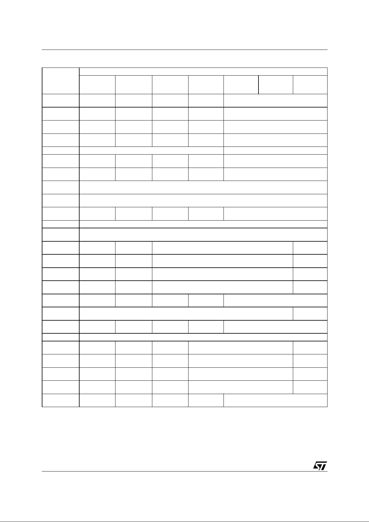
M36W216TI, M36W216BI
60/62
Table 34. Write State Machine Current/Next, sheet 2 of 2.
Note: Cmd = Command, Elect.Sg. = Electronic Signature, Pro g. = Program, Pro t = P rot ection.
Current State
Command Input (and Next State)
Read Ele ct.Sg.
(90h)
Read CFI
Query
(98h)
Lock Setup
(60h)
Prot. Prog.
Setup (C0h)
Lock Confirm
(01h)
Lock Down
Confirm (2Fh)
Unlock
Confirm
(D0h)
Read Array Read Elect.Sg. Read CFI Query Lock Setup
Prot. Prog.
Setup
Read Array
Read Status Read Elect.Sg. Read CFI Query Lock Setup
Prot. Prog.
Setup
Read Array
Read Ele ct .Sg. Read El ect.Sg. Read CFI Q uery Lock Set up
Prot. Prog.
Setup
Read Array
Read CFI Query Read Elect.Sg. Read CFI Query Lock Setup
Prot. Prog.
Setup
Read Array
Lock Setup Lock Com m and Error Loc k (c o m plete)
Lock Cmd Error Read Elect.Sg. Read CFI Query Lock Setup
Prot. Prog.
Setup
Read Array
Lock (comple te) Read Elect.Sg. Read CFI Query Lock Setup
Prot. Prog.
Setup
Read Array
Prot. Prog.
Setup
Protectio n Register P rogram
Prot. Prog.
(continue)
Protection Register Program (continue)
Prot. Prog.
(complete)
Read Elec t.Sg. Read CFI Query Lock Setu p
Prot. Prog.
Setup
Read Array
Prog. Setup Program
Program
(continu e)
Program (continue)
Prog. Suspend
Read Status
Prog. Suspend
Read Elec t.Sg.
Prog. Suspend
Read CFI Query
Program Suspend Read Array
Program
(continue)
Prog. S uspend
Read Array
Prog. Suspend
Read Elec t.Sg.
Prog. Suspend
Read CFI Query
Program Suspend Read Array
Program
(continue)
Prog. S uspend
Read El ect.Sg.
Prog. Suspend
Read Elec t.Sg.
Prog. Suspend
Read CFI Query
Program Suspend Read Array
Program
(continue)
Prog. S uspend
Read CFI
Prog. Suspend
Read Elec t.Sg.
Prog. Suspend
Read CFI Query
Program Suspend Read Array
Program
(continue)
Program
(complete)
Read Elect.Sg. Read CFIQuery Lock Setup
Prot. Prog.
Setup
Read Array
Erase Setup Erase Command Error
Erase
(continue)
Erase
Cmd.Error
Read Elec t.Sg. Read CFI Query Lock Set up
Prot. Prog.
Setup
Read Array
Erase (con tinue) Erase (continu e)
Erase Suspend
Read Status
Erase Suspend
Read Elec t.Sg.
Erase Suspend
Read CFI Query
Lock Setup Erase Suspend Read Ar ray
Erase
(continue)
Erase Suspend
Read Array
Erase Suspend
Read Elec t.Sg.
Erase Suspend
Read CFI Query
Lock Setup Erase Suspend Read Ar ray
Erase
(continue)
Erase Suspend
Read El ect.Sg.
Erase Suspend
Read Elec t.Sg.
Erase Suspend
Read CFI Query
Lock Setup Erase Suspend Read Ar ray
Erase
(continue)
Erase Suspend
Read CFI Query
Erase Suspend
Read Elec t.Sg.
Erase Suspend
Read CFI Query
Lock Setup Erase Suspend Read Ar ray
Erase
(continue)
Erase
(complete)
Read Elec t.Sg. Read CFI Query Lock Setu p
Prot. Prog.
Setup
Read Array
Page 61

61/62
M36W216TI, M36W216BI
REVISION HIST ORY
Table 35. Document Revision History
Date Version Revision Details
19-Nov-2002 1.0 First Issue
Page 62

M36W216TI, M36W216BI
62/62
Information furnished is believed to be accurate an d rel i able. However, STMicroelectro ni cs assumes no responsibilit y for the cons equences
of use of such information nor for any infringement of patents or other rights of third parties which may result from its use. No license is granted
by implic ation or otherwise under any patent or patent rights of STMi croelectr onics. Specifications mentioned in th i s publication are subject
to change without notice. This publication supersedes and replaces all information previously supplied. STMicroelectronics products are not
authoriz ed for use as critical comp onents in lif e support devi ces or systems wi thout exp ress written approval of STM i croelect ronics.
The ST logo i s registered trademark of STMicroel ectronics
All other nam es are the pro perty of their respective owners
© 2002 STMicroelectronics - All Rights Reserved
STMicroelectron ic s group of com panies
Austra lia - Brazil - Can ada - China - Finl and - France - Germany - Hong Kong -
India - Israel - Italy - Japan - Malaysia - Malt a - M orocco - Singapore - Spa i n - Sweden - Swi tzerland - United Kin gdom - United States.
www.st.com
 Loading...