

Page 1
M36W108AT
M36W108AB
8 Mbit (1Mb x8, Boot Block) Flash Memory and
1 Mbit (128Kb x8) SRAM Low Voltage Multi-Memory Product
PRELIMINARY DATA
■ SUPPLY VOLTAGE
CCF
= V
–V
Erase and Read
■ ACCESS TIME: 100ns
■ LOW POWER CONSUMPTION
– Read: 40mA max. (SRAM chip)
– Stand-by: 30µA max. (SRAM chip)
– Read: 10mA max. (Flash chip)
– Stand-by: 100µA max. (Flash chip)
FLASH MEMORY
■ 8 Mbit (1Mb x 8) BOOT BLOCK ERASE
■ PROGRAMMING TIME: 10µs typical
■ PROGRAM/ERASE CONTROLLER (P/E.C.)
– Program Byte-by-Byte
– Status Register bits and Ready/Busy Output
■ SECURITY PROTECTION MEMORY AREA
■ INSTRUCTION ADDRESS CODING: 3 digits
■ MEMORY BLOCKS
– Boot Block (Top or Bottom location)
– Parameter and Main Blocks
■ BLOCK, MULTI-BLOCK and CHIP ERASE
■ ERASE SUSPEND and RESUME MODES
– Read and Program another Block during
Erase Suspend
■ 100,000 PROGRAM/ERASE CYCLES per
BLOCK
■ ELECTRONIC SIGNATURE
– Manufacturer Code: 20h
– Device Code, M36W108AT: D2h
– Device Code, M36W108AB: DCh
= 2.7V to 3.6V: for Program,
CCS
BGA
LBGA48 (ZM)
6 x 8 solder balls
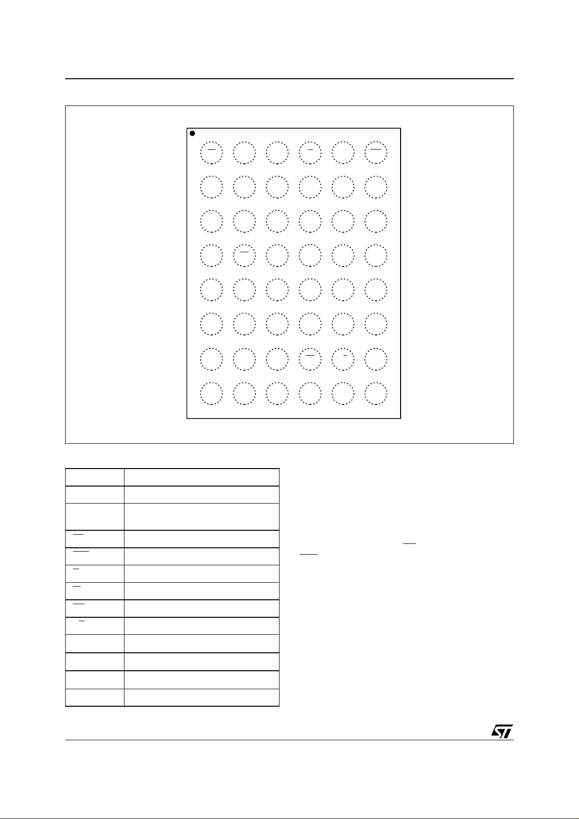
Figure 1. Logic Diagram
V
CCF
20
A0-A19
W
EF
G
RP
E1S
E2S
M36W108AT
M36W108AB
LGA48 (ZN)
6 x 8 solder lands
V
CCS
8
LGA
DQ0-DQ7
RB
SRAM
■ 1 Mbit (128Kb x 8)
■ POWER DOWN FEATURES USING TWO
V
SS
CHIP ENABLE INPUTS
■ LOW V
March 1999
This is preliminary information on a new product now in development or undergoing evaluation. Details are subject to change without notice.
DATA RETENTION: 2V
CC
AI02620
1/36
Page 2
M36W108AT, M36W108AB
Figure 2. LBG A and LGA Connection s (Top V iew)
654321
A
B
C
D
E
F
G
H
W
CCS
A17
SS
NC
CCF
A11A14
A8A18V
NC
G
DQ7 DQ5
DQ0
A6
A19
RP
A16NC
A10 E1S
V
DQ1DQ2DQ4A5NC
A0
A1NCEFV
A2A3DQ3NCNC
A4A7V
E2SRBA13DQ6NC
A9A15A12NC
SS
AI02508
Table 1. Signal Names
A0-A16 Address Inputs
A17-A19 Address Inputs for Flash Chip
DQ0-DQ7
EF
, E2S Chip Enable for SRAM Chip
E1S
G
W
RP
RB
V
CCF
V
CCS
V
SS
NC Not Connected Internally
2/36
Data Input/Outputs, Command Inputs
for Flash Chip
Chip Enable for Flash Chip
Output Enable
Write Enable
Reset for Flash Chip
Ready/Busy Output for Flash Chip
Supply Voltage for Flash Chip
Supply Voltage for SRAM Chip
Ground
DESCRIPTION
The M36W108A is multi-chip device containing an
8 Mbit boot block Flash memory and a 1 Mbit of
SRAM. The device is offered in the new Chip
Scale Package solutions: LBGA48 1.0mm ball
pitch and LGA48 1.0mm land pitch.
The two components, of the package’s overall 9
Mbit of memory, are distinguishable by use of the
three chip enable lines: E F
E1S
and E2S for the SRAM.
for the Flash memory,
The Flash memory component is identical with the
M29W008A device. It is a non-volatile memory
that may be erased electrically at the block or chip
level and programmed in-system on a Byte-byByte basis using only a single 2.7V to 3.6V V
CCF
supply. For Program and Erase operations the
necessary high voltages are gen erated internally.
The device can also be programmed in standard
programmers. The array matrix organizat ion allows each block to be e rased and reprogrammed
without affecting other blocks.
Instructions for Read/Reset, Auto Select for reading the Electronic Signature, Programming, B lock
Page 3
M36W108AT, M36W108AB
Table 2. Absolute Maximum Ratings
Symbol Parameter Value Unit
T
A
T
BIAS
T
STG
(2)
V
IO
V
CCF
V
CCS
V
(EF, RP)
PD Power Dissipation 0.7 W
Note: 1. Except for the rating "O perating T em perature R ange", stresses abo ve those listed in the T able "Absolute Maxi m um Ratings" may
cause permanent damage to the device. These are stress ratings only and operation of the device at these or any other conditions
above those indi cated in t he Operating sect i ons of thi s specifi cation i s not impl i ed. Exposure to Absolute M aximum Rating c onditions for extended per iods may aff ect device reliabilit y. Refer also to the STMicroel ectronics SURE Program an d other relevan t qual ity docum en ts .
2. Minimum Voltage may undershoot to –2V during transiti on and for less t han 20ns.
3. Depends on range.
Ambient Operating Temperature
Temperature Under Bias –50 to 125 °C
Storage Temperature –65 to 150 °C
Input or Output Voltage
Flash Chip Supply Voltage –0.6 to 5 V
SRAM Chip Supply Voltage –0.3 to 4.6 V
EF, RP Voltage 0.6 to 13.5 V
and Chip Erase, Erase Suspend and Resume are
written to the device in cycles of comm ands to a
Command Interface usi ng standard m icroprocessor write timings.
The SRAM compone nt is a low power SRAM that
features fully static operation requiring no external
clocks or timing strobes, with e qual address access and cycle times. It requires a single 2.7V to
3.6V V
supply, and all inputs and outpu ts are
CCS
TTL compatible.
SIGNAL DESCRIPTIONS
See Figure 1 and Table 1.
Address Inputs (A0-A16). Addres ses A0 t o A16
are common inputs for the Flash chip and the
SRAM chip. The address inputs for the Flash
memory or the SRAM array are l atched during a
write operation on the falling edge of Flash Chip
Enable (EF
Write Enable (W
), SRAM Chip Enable (E 1S or E2S) or
).
Address Inputs (A17-A19). Address A17 t o A 19
are address inputs for the Flash chip. They are
latched during a write operation on the falling edge
of Flash Chip Enable (EF
) or Write Enable (W).
Data Input/Outputs (DQ0-DQ7). The input is
data to be programmed in the Flash or SRAM
memory array or a command to be written to the
C.I. of the Flash chip. Both are latched on the rising edge of Flash Chip Enable (EF
Enable (E1S
or E2S) or Write Enable (W). The
output is data from the Flash memory or SRAM array, the Electronic Signature Manufacturer or Device codes or the Status register Dat a Polling bit
(1)
(3)
), SRAM Chip
–40 to 85 °C
–0.5 to V
CC
+0.5
V
DQ7, the Toggle Bits DQ6 and DQ2, the Error bit
DQ5 or the Erase Timer bit DQ3. Outputs are valid
when Flash Chip Enable (EF
able (E1S
or E2S) a nd O utp ut Enable (G ) are ac-
) or SRAM Chip En-
tive. The output is high impedance when the both
the Flash chip and the SRAM chip are deselected
or the outputs are disabled and when Reset (R P
is at a V
Flash Chip Enable (EF
.
IL
). The Chip Enable input
for Flash activates the memory control logic, input
buffers, decoders and sense a mpl ifiers. E F
at V
deselects the memory and reduces the power consumption to the standby level. EF
can also be
used to control writing to the command register
and to the Flash memory array, while W
at V
. It is not allowed to set EF at VIL, E1S at V
IL
remains
and E2S at VIH at the same time.
SRAM Chip Enable (E1S
, E2S). The Chip En-
able inputs for SRAM activate the memory control
logic, input buffers, decoders and sense amplifiers. E1S
at VIH or E2S at VIL deselects the mem ory and reduces the power consumption to the
standby level. E1S
and E2S can also be used to
control writing to the SRAM memory array, while
W
remains at VIL. It is not allowed to set EF at VIL,
E1S
at VIL and E2S at VIH at the same time.
Output Enable (G
). The Output Enable gates the
outputs through the data buffers during a read operation. When G
is High the outpu ts are High im-
pedance.
Write Enable (W
). The Write Enable input con-
trols writing to the Command Register of the Flash
chip and Address/Data latches.
)
IH
IL
3/36
Page 4
M36W108AT, M36W108AB
Table 3. Main Operation M od es
(1)
Operation Mode EF E1S E2S G W RP DQ7-DQ0
Flash Chip Read
SRAM Chip Read
Flash Chip Write
SRAM Chip Write
Flash Chip Output Disable
SRAM Chip Output Disable
Flash Chip Stand-by
Flash Chip Reset
SRAM Chip Stand-by
Note: 1. X = VIL or VIH.
V
IL
V
IL
V
IH
V
IL
V
IL
V
IH
X
V
IH
X
V
IL
V
IH
X
V
IL
V
IH
XX
V
IH
V
IH
X
V
IL
XX
V
IH
XX
X
V
IH
XX
X
V
IL
V
IH
X
V
IL
V
IH
X
V
IL
V
IH
XXX
V
IL
XXX
V
IL
V
IL
V
IL
V
IL
V
IH
V
IH
X
V
IH
V
IH
V
IH
V
IH
V
IH
V
IH
V
IL
V
IL
V
IL
V
IH
V
IH
V
IH
XX
XX
XX
V
IH
V
IH
X Data Output
V
IH
V
IH
X Data Input
XHi-Z
XHi-Z
XHi-Z
V
IH
V
IL
V
IL
V
IL
V
IL
Data Output
Data Output
Data Input
Data Input
Hi-Z
Hi-Z
Hi-Z
Hi-Z
Hi-Z
Reset Input (RP). The Reset input provides
hardware reset of the Flash chip. Reset of the
Flash memory is achieved by pulling RP
at least t
. When the reset pulse is given, if the
PLPX
to VIL for
Flash memory is in Read or Standby modes, it will
be available for new operations in t
rising edge of RP
.
PHEL
after the
If the Flash memory is in E rase or P rogram m ode
the reset w ill take t
Busy (RB
) signal will be held at VIL. The end of the
during which the Ready/
PLYH
Flash memory reset will be ind icated by the rising
edge of RB
. A hardware reset during an Erase or
Program operation will corrupt the data being programmed or the block(s) being erased. See Table
18 and Figure 10.
Ready/Busy Output (RB
). Ready/Busy is an
open-drain output of the Flash chip. It gives the internal state of the Program/Erase Controller (P/
E.C.) of the Flash device. When RB
is Low, the
Flash device is busy with a Program or Erase operation and it will not a ccept any additional program or erase instructions except the Erase
Suspend instruction. When RB
is High, the Flash
device is ready for any Read, Program or Eras e
operation. The RB
will also be High when the
Flash memory is put in Erase Suspend or Standby
modes.
V
Supply Voltag e . Fl ash m em ory powe r su p-
CCF
ply for all operations (Read, Program and Erase).
V
Supply Voltage. SRAM power supply for
CCS
all operations (Read, Program).
V
Ground. VSS is the reference for all voltage
SS
measurements.
POWE R SU PPLY
Power Up. The Flash memory Command Inter-
face is reset on power up to Read Array . Either
Flash Chip Enable (EF
must be tied to V
) or Write Enable (W) inputs
during Power Up to allow max-
IH
imum security and the possib ility to write a command on the first rising edge of EF
write cycle initiation is blocked when V
V
.
LKO
and W . Any
is below
CCF
Supply Rails. Normal precautions must be taken
for supply voltage decoupling; each device in a
, V
system should have the V
CCF
pled with a 0.1µF capacitor close to the V
V
and VSS pins. The PCB trace widths sho uld
CCS
be sufficient to carry t he V
currents and the V
erase current required.
CCF
CCF
and V
rails decou-
CCS
CCS
CCF
program
,
4/36
Page 5
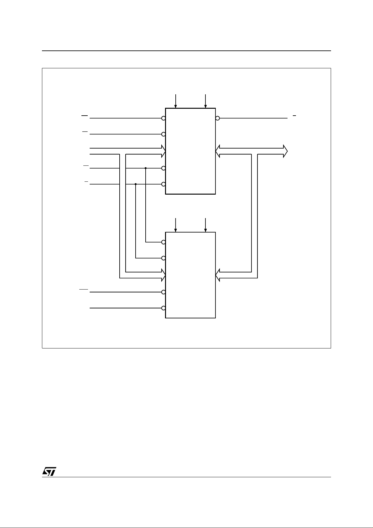
Figure 3. Internal Function a l Arrangement
M36W108AT, M36W108AB
V
CCF
RP RB
EF
A0-A19 DQ0-DQ7
W
G
A0-A16
Flash Memory
(1Mb x 8)
V
CCS
1 Mbit SRAM
(128 Kb x 8)
8 Mbit
V
SS
V
SS
E1S
E2S
AI02444
5/36
Page 6
M36W108AT, M36W108AB
FLASH MEMORY COMPONENT
Organization and Architecture
Organization. The Flash chip is organized as
1Mbit x 8. The m emory uses the address inputs
A0-A19 and the Data Input/Outputs DQ0-DQ7.
Memory control is provided by Chip Enable (EF
Output Enable (G
) and Write Enable (W) inputs.
Erase and Program operations are controlled by
an internal Program/Erase Controller (P/E.C.).
Status Register data output on DQ7 provides a
Data Polling signal, while Status Register data outputs on DQ6 and D Q2 provide Toggle signals to
indicate the state of the P/E.C. operations. A
Ready/Busy (RB
) output indicates the c ompletion
of the internal algorithms.
Memory Blocks. The device features asymmetri-
cally blocked architecture providing system memory integration. Both Top and Bottom Boot Block
devices have an array of 19 blocks, one Boot
Block of 16K Bytes, two P arameter Blocks of 8K
Bytes, one Main Block of 32K Bytes a nd fifteen
Main Blocks of 64K Bytes. The Top Boot Block
Table 4. Top Boot Block, Flash Block Address
Size (KWord) Address Range
16 FC000h-FFFFFh
8 FA000h-FBFFFh
8 F8000h-F9FFFh
32 F0000h-F7FFFh
64 E0000h-EFFFFh
64 D0000h-DFFFFh
64 C0000h-CFFFFh
64 B0000h-BFFFFh
64 A0000h-AFFFFh
64 90000h-9FFFFh
64 80000h-8FFFFh
64 70000h-7FFFFh
64 60000h-6FFFFh
64 50000h-5FFFFh
64 40000h-4FFFFh
64 30000h-3FFFFh
64 20000h-2FFFFh
64 10000h-1FFFFh
64 00000h-0FFFFh
version has the Boot Block at the top of the mem ory address space and the Bottom Boot Block version locates the Boot Block starting at the bottom.
The memory maps and bl ock address tables are
showed in Figures 4, 5 and Tables 4, 5. Each
block can be e rased sepa rately, any combi nation
),
of blocks can be specified for mult i-block erase or
the entire chip may be erased . The Erase operations are managed automatically by the P/E.C.
The block erase operation can be s uspended in
order to read from or program to any block not being erased, and then resumed.
Device Operations
The following operations can be performed using
the appropriate bus cycles: Read Array, Write
command, Output Disable, Standby and Reset
(see Table 6).
Read. Read operations are used to output the
contents of the Memory Array, the Electronic Signature or the Status Register. Both Chip Enable
) and Output Enable (G) must be low, with
(EF
Write Enable (W
) high, in order to read t he ou tput
of the memory.
Table 5. Bottom Boot Block, Flash Block
Address
Size (KWord) Address Range
64 F0000h-FFFFFh
64 E0000h-EFFFFh
64 D0000h-DFFFFh
64 C0000h-CFFFFh
64 B0000h-BFFFFh
64 A0000h-AFFFFh
64 90000h-9FFFFh
64 80000h-8FFFFh
64 70000h-7FFFFh
64 60000h-6FFFFh
64 50000h-5FFFFh
64 40000h-4FFFFh
64 30000h-3FFFFh
64 20000h-2FFFFh
64 10000h-1FFFFh
32 08000h-0FFFFh
8 06000h-07FFFh
8 04000h-05FFFh
16 00000h-03FFFh
6/36
Page 7
M36W108AT, M36W108AB
Write. Write operations are u sed to give Ins truc-
tion Commands to the memory or to latch input
data to be programmed. A write operation is initiated when Chip Enable (EF
able (W
) is at VIL with Output Enable (G) a t VIH.
Addresses are latched on t he falling edge of W
EF
whichever occurs last. Commands and Input
Data are latched on the rising edg e of W
) is Low and Write En-
or
or EF
whichever occurs first.
Output Disa bl e . The data outputs are high im-
pedance when the Output Enable (G
Write Enable (W
) at VIH.
) is at VIH with
Standby. T he memory is in standby when Chip
Enable (EF
) is at VIH and the P/E.C. is idle. The
power consumption is reduced to the standby level
and the outputs are high impedance, independent
of the Output Enable (G
) or Write Enable (W) in-
puts.
Automatic Standby. After 150ns of bus inactivity
and when CMOS levels are driving the addresses,
the chip automatically enters a pseudo-standby
mode where consumption is reduced to the CMOS
Instructions and Commands
Seven instructions are defined (see Table 7) to
perform Read Array, Auto Select (to read the Electronic Signature), Program, Block Erase, Chip
Erase, Erase Suspend and Erase Resume. The
internal P/E.C. automatically handles all timing
and verification of the Program and Erase operations. The Status Register Data Polling, Toggle,
Error bits and the RB
output may be read at any
time, during programming or erase, to monitor the
progress of the operation.
Instructions, made up of commands wri tten in cycles, can be given to the Program/Erase Controller
through a Command Interface (C.I.).
The C.I. latches commands written to the memory.
Commands are made of address and data sequences. Two coded cycles unlock the Command
Interface. They are followed by an input command
or a confirmation command. The coded sequence
consists of writing the data AAh at the address
5555h during the first cycle and the data 55h at the
address 2AAAh during the second cycle.
standby value, while outputs still drive the bus.
Table 6. Flash User Bus Operations
Operation EF G W RP A15 A12 A9 A6 A1 A0 DQ7-DQ0
Read Byte
Write Byte
Output Disable
Stand-by
Reset X X X
Note: 1. X = VIL or VIH.
V
V
V
V
IL
IL
IL
IH
V
IL
V
IH
V
IH
XX
(1)
V
V
V
V
IH
IL
IH
A15 A12 A9 A6 A1 A0 Data Output
IH
V
A15 A12 A9 A6 A1 A0 Data Input
IH
V
V
V
XXXXXX Hi-Z
IH
XXXXXX Hi-Z
IH
XXXXXX Hi-Z
IL
Table 7. Read Flash Electronic Signature
Code Device EF
Manufact. Code
M36W108AT
Device Code
M36W108AB
V
IL
V
IL
V
IL
G W A1 A0
V
IL
V
IL
V
IL
V
IH
V
IH
V
IH
V
IL
V
IL
V
IL
Other
Addresses
V
V
V
Don’t care 20h
IL
Don’t care D2h
IH
Don’t care DCh
IH
DQ7-DQ0
7/36
Page 8
M36W108AT, M36W108AB
Table 8. Flash Commands
Hex Code Command
00h Invalid/Reserved
10h Chip Erase Confirm
20h Reserved
30h Block Erase Resume/Confirm
80h Set-up Erase
90h
A0h Program
B0h Erase Suspend
F0h Read Array/Reset
Read Electronic Signature/
Block Protection Status
Instructi ons a re co mpose d of up to si x cycles. The
first two cycles input a Coded Sequence to the
Command Interface which is common to all instructions (s ee Tab le 9). The third cycl e i nput s th e
instruction set-up command. Subsequent cycles
output the addressed data or Electronic Signature
for Read operations. In order to give additional
data protection, the instructions for Program and
Block or Chip Erase require further command inputs. For a Program instru ction, the fourth command cycle inputs the address and data to be
programmed. For an Erase instruction (block or
chip), the fourth and fifth cycles input a further
Coded Sequence before the Erase confirm command on the sixth cycle. Erasure of a memory
block may be suspended, in order to read data
from another block or to program da ta in another
block, and then resumed.
When power is first applied or if V
, the command interface is reset to Read Ar-
V
LKO
falls be low
CCF
ray.
Command sequencing must be followed exactly.
Any invalid combination of commands will reset
the device to Read Array. The inc reased number
of cycles has been chosen to assure maximum
data security.
Read/Reset (RD) Instruction. The Read/Reset
instruction consists of one write cycle giving the
command F0h. It can be optionally preceded by
the two Coded cycles. Subsequent read operations will r ead the memory array a ddressed and
output the data read. A wait state of t
PLYH
is necessary after Read/Reset prior to any valid read if
the memory was in an Erase or Program mode
when the RD instruction is given (see Table 18
and Figure 10).
Auto Select (AS) Instruction. This instruction
uses the two Coded cycles followed by one write
cycle giving the c ommand 90h to addres s 5555h
for command set-up. A subsequent read will output the Manufacturer Code or the Device Code
(Electronic Signature) depending on the levels of
A0 and A1 (see Table 7). The Electronic Signature
can be read from the memory allowing programming equipment or applications to automatically
match their interface to the characteristics of the
Flash memory. The Manufacturer Code, 20h, is
output when the addresses lines A0 and A1 are at
, the Device Code is output whe n A0 is at V
V
IL
IH
with A1 at VIL. Other address inputs are ignored.
Program (PG) Instru ctio n . This in struction uses
four write cycles. The Program command A0h is
written to address 5555h on the third cycle after
two Coded Cycles. A fourth write operation latches the Address and the Data to be written and
starts the P/E.C. Read operations output the Status Register bits after the programming has started. Memory programming i s m ade only by writing
’0’ in place of ’1’. Status bits DQ6 and DQ7 determine if programming is on-going and DQ5 allows
verification of any possible error. Programming at
an address not in blocks being erased is also possible during erase suspend. In t his case, DQ 2 wi ll
toggle at the address being programmed.
8/36
Page 9

M36W108AT, M36W108AB
Block Erase (BE) Instruction. This instruction
uses a minimum of six write cycles. The Erase
Set-up command 80h is written to address 5555h
on third cycle after the two Coded cycles. The
Block Erase Confirm command 30h is similarly
written on the sixth cycle after another two Coded
Cycles. During the input of the second comm and
an address within the b lock to be erased is given
and latched into the memory.
Additional block Erase Confirm commands and
block addresses can be written subsequently to
erase other blocks i n paral l el, wit h out fu rthe r Co ded cycles. The erase will start after the erase timeout period (see Erase Timer Bit DQ3 description).
Thus, additional Erase Confirm commands for other blocks must be given within this delay. The input
of a new Erase Confirm command will restart the
timeout period. The status of the internal timer can
be monitored through the level of DQ3, if DQ3 is ’0’
the Block Erase Command has been given and
the timeout is running, if DQ3 is ’1’, the timeout has
expired and the P/E.C. is erasing the block(s). If
the second command gi ven is not an erase confirm or if the Coded cy cles are wrong, the instruction aborts, and the device is reset to Read Array.
It is not necessary to program the block with 00h
as the P/E.C. will do this automatically before to
erasing to FFh. Read operations after the sixth rising edge of W
or EF output the Status Register
bits.
During the execution of the erase by the P/E.C.,
the memory only accepts the Erase Suspend (ES)
and Read/Reset (RD) instructions. A Read/Reset
command will definitively abo rt erasure and result
in invalid data in blocks being erased. A complete
state of the block erase operation is given by the
Status Register bits (see DQ2, DQ3, DQ5, DQ 6
and DQ7 description).
Chip Erase (CE) Instruction. This instruction
uses six write cycles. The Erase Set- up command
80h is written to address 5555h on the third cycle
after the two Coded Cycles. The Chip Erase Confirm command 10h is similarly written on the sixth
cycle after another two Coded Cycles. If the sec-
ond command given is not an erase confirm or if
the Coded Sequence is wrong, the instruction
aborts and the device is reset to Read Array. It is
not necessary to program the array with 00h first
as the P/E.C. will automatically do this before
erasing it to FFh. Read operations after the sixth
rising edge of W
or EF output the Status Register
bits. A complete state of the chip erase o peration
is given by the Status Register bits (see DQ2,
DQ3, DQ5, DQ6 and DQ7 description).
Erase Suspend (ES) Instruction. The Block
Erase operation may be suspended by this instruction which consists of writing the command
B0h without any specific address. No Coded Cycles are required. It permits reading of data from
another block and progra mming in another block
while an erase operation is in progress. Erase suspend is accepted only during the Block Erase instruction execution. Writing this command du ring
the erase timeout period will, in addition to suspending the erase, terminate the timeout. The
Toggle bit DQ6 stops toggling when the P /E.C. is
suspended. The Toggl e bits will stop toggling be-
tween 0.1µs and 15µs after the Erase Suspend
(ES) command has been written. Th e device will
then automatically be set to Read Mem ory Array
mode. When erase is suspended, a Read from
blocks being erased will output DQ 2 toggling and
DQ6 at '1'. A Read from a block not being erased
returns valid data. During suspension the memory
will respo nd only to the Erase Resu me (ER) a nd
the Program (PG) instructions. A Program operation can be initiated during Erase Suspend in one
of the blocks not being erased. It will result in both
DQ2 and DQ6 toggling when the data is being programmed. A Read/Reset command will definitively
abort erasure and result in invalid data in the
blocks being erased.
Erase Resume (ER) Instruction. If an Erase
Suspend instruction was previously exec uted, the
erase operation may be resumed by giving the
command 30h, at any address, and without any
Coded cycles.
9/36
Page 10
M36W108AT, M36W108AB
Table 9. Flash Instructions
(1)
Mne. Instr. Cyc. 1st Cyc. 2nd Cyc. 3rd Cyc. 4th Cyc. 5th Cyc. 6th Cyc. 7th Cyc.
Read/Reset
(2,4)
RD
Memory
Array
(4)
AS
Auto Select 3+
PG Program 4
BE Block Erase 6
(3,6)
Addr.
1+
Data F0h
(3,6)
Addr.
3+
Data AAh 55h F0h
(3,6)
Addr.
Data AAh 55h 90h
(3,6)
Addr.
Data AAh 55h A0h
(3,6)
Addr.
X
Read Memory Array until a new write cycle is initiated.
555h 2AAh 555h
Read Memory Array until a new write cycle
is initiated.
555h 2AAh 555h
Read Electronic Signature until a new write
cycle is initiated. See Note 5.
555h 2AAh 555h
Program
Address
Program
Read Data Polling or Toggle Bit
until Program completes.
Data
555h 2AAh 555h 555h 2AAh
Block
Address
Additional
Block
Data AAh 55h 80h AAh 55h 30h 30h
(3,6)
CE Chip Erase 6
Addr.
555h 2AAh 555h 555h 2AAh 555h
Note 8
Data AAh 55h 80h AAh 55h 1 0h
(3,6)
ES
Note: 1. Commands not interpreted in this table will default to read array mode.
Suspend
Erase
ER
Resume
2. A wait of t
starting any new operation (see Tabl e 15 and Figure 8).
3. X = Don’t care.
4. The f i rst cycles of the RD or AS instructions are follo wed by read operations. Any number of read cycles can occur after the command cycl e s.
5. Signature Address bits A0, A1, at V
code.
6. For C oded cycles address input s A 11-A19 are do n’ t care.
7. Optional, addi tional Bl ocks add resses mus t be ent ered withi n the era se timeo ut delay af ter last write ent ry, timeout statu s can be
verified t hrough DQ3 value (see Eras e Timer Bit DQ3 description). When full com m and is e ntered, re al Data Po l ling or To ggle bit
until Erase is completed or suspended.
8. Rea d Data Polli ng, Toggle bits or RB
9. Duri ng Erase Suspend, Read and Data Program functions are allow ed in blocks not being erased.
is necessary after a Read/Reset command if the memory was in an Erase, Erase Suspend or Program mode before
PLYH
Erase
(9)
Addr.
1
Data B0h
(3,6)
Addr.
1
Data 30h
IL
X
Read until Toggle stops, then read all the data needed from any
Block(s) not being erased then Resume Erase.
X
Read Data Polling or Toggle Bits until Erase completes or Erase
is suspended another time.
will output Manufacturer code (20h). Address bits A0 at VIH and A1, at VIL will output Device
until Erase complete s.
(7)
10/36
Page 11
M36W108AT, M36W108AB
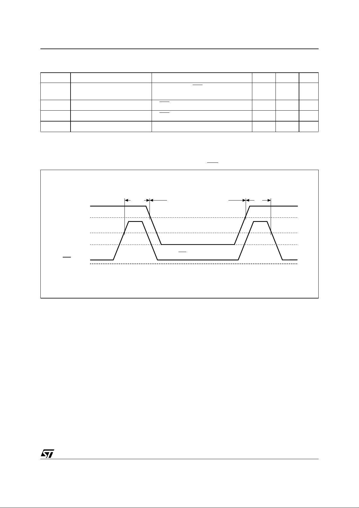
Table 10. Flash Status Register Bits
DQ Name Logic Level Definition Note
‘1’
Data
7
Polling
6 Toggle Bit
5 Error Bit
4 Reserved
Erase
3
Time Bit
2 Toggle Bit
‘0’ Erase On-going
DQ
DQ
‘-1-0-1-0-1-0-1-’ Erase or Program On-going
DQ Program Complete
‘-1-1-1-1-1-1-1-’
‘1’ Program or Erase Error
‘0’ Program or Erase On-going
‘1’ Erase Timeout Period Expired
‘0’
‘-1-0-1-0-1-0-1-’
‘1’
(1)
Erase Complete or erase block
in Erase Suspend
Program Complete or data of
non erase block during Erase
Suspend
Program On-going
Erase Complete or Erase
Suspend on currently
addressed block
Erase Timeout Period
On-going
Chip Erase, Erase or Erase
Suspend on the currently
addressed block.
Erase Error due to the
currently addressed block
(when DQ5 = ‘1’)
Program on-going, Erase
on-going on another block or
Erase Complete
Indicates the P/E.C. status, check during
Program or Erase, and on completion before
checking bits DQ5 for Program or Erase
Success.
Successive reads output complementary
data on DQ6 while Programming or Erase
operations are on-going. DQ6 remains at
constant level when P/E.C. operations are
completed or Erase Suspend is
acknowledged.
This bit is set to ‘1’ in the case of
Programming or Erase failure.
P/E.C. Erase operation has started. Only
possible command entry is Erase Suspend
(ES).
An additional block to be erased in parallel
can be entered to the P/E.C.
Indicates the erase status and allows to
identify the erased block.
DQ
1 Reserved
0 Reserved
Note: 1. Logic level ‘1’ is High, ‘0 ’ is Low. -0-1-0-0-0-1-1-1-0- represent bit value in successive Read operations.
Erase Suspend read on non
Erase Suspend block
11/36
Page 12
M36W108AT, M36W108AB
Table 11. F lash Polling an d To ggle Bits
Mode DQ7 DQ6 DQ2
Program DQ7
Erase 0 Toggle Note 1
Erase Suspend Read
(in Erase Suspend
block)
Erase Suspend Read
(outside Erase Suspend
block)
Erase Suspend Program DQ7
Note: 1. Toggle if the addr ess is within a bl ock being eras ed.
‘1’ if the address is withi n a block not being erased.
DQ7 DQ6 DQ2
Toggle 1
1 1 Toggle
Toggle N/A
(1)
Status Register Bits
P/E.C. status is indicated during execution by Data
Polling on D Q7, detection of T oggle on DQ6 and
DQ2, or Error on DQ5 and E ras e T imer DQ3 bits.
Any read attempt during P rogram or Erase command execution will automatically output these
five Status Register bits. The P/E.C. automatically
sets bits DQ2, DQ 3, DQ5, DQ6 and DQ7. Other
bits (DQ0, DQ1 and D Q4) a re reserved for future
use and should be masked (see Table 10 and Table 11).
Data Polling Bit (DQ7). When Program ming operations are in progress, this bit out puts the complement of the bit being programmed on DQ7.
During Erase operation, it outputs a ’0’. After completion of the operation, DQ7 will output the bit last
program me d or a ’1 ’ after er asi ng. Data Pollin g is
valid and only effective during P/E.C. operation,
that is after the fourth W pulse for programming or
after the sixth W
pulse for erase. It must be performed at the address being programmed or at an
address within the block being erased. If all the
blocks selected for erasure are protected, DQ7 will
be set to '0' for about 100µs, and then return to the
previous addressed memory data value. See Figure 10 for the Data Polling flowchart and Figure 12
for the Data Polling waveforms. DQ7 will also flag
the Erase Suspen d mode by switching from '0' to
'1' at the start of the Erase Suspend. In order to
monitor DQ7 in t he Erase Sus pend mode an address within a block being erased must be provided. For a Read Operation in Erase Suspend
mode, DQ7 will output '1' if the read is attempted
on a block being erased and the data value on oth-
er blocks. During Program operation in Erase Suspend Mode, DQ7 will have the same behaviour as
in the normal program execution outside of the
suspend mode.
Toggle Bit (D Q6). When Programming or Erasing operations are in progress, successive attempts to read DQ6 will output complementary
data. DQ6 will toggle following toggling of either G
when G is at VIL. The operation is complet-
or EF
ed when two successive reads yield the same output data. The next read will output the bit last
programmed or a '1' after erasing. The toggle bit
DQ6 is valid only during P/E.C. operations, that is
after the fourth W
the sixth W
pulse for programming o r after
pulse for Erase. If the blocks selected
for erasure are protected, DQ6 will toggle for about
100µs and then return ba ck to Read. DQ6 will be
set to '1' if a Read operation is at tempted on an
Erase Suspend block. When erase is suspended
DQ6 will toggle during programming operations in
a block different to the block in Erase Suspend. Either EF
or G toggling will cause DQ6 to toggle.
See Figure 12 for Toggle Bit f lowcha rt an d Figure
15 for Toggle Bit waveforms.
Toggle Bit (D Q2). This toggle bit, together with
DQ6, can be used to det ermine the d evice status
during the Erase operations. It can also be used to
identify the block being erased. During Er ase or
Erase Suspend a read from a block bei ng erased
will cause DQ2 to toggle. A r ead from a block not
being erased will set DQ2 to '1' during erase and
to DQ2 during Erase Suspend. During Chip Erase
a read operation will cause DQ 2 to toggle as all
blocks are b eing erased. DQ 2 will be set to '1' dur ing program operation and when erase is complete. After erase completion and if the error bit
DQ5 is set to '1', DQ2 will toggle if the faulty block
is addressed.
Error Bit (DQ5). This bit is set to '1' by the P/E.C.
when there is a failure of programming, block
erase, or chip erase that results in invalid data in
the memory block. In case of an error in block
erase or program, the block in wh ich t he error occurred or to which the program me d da ta belon gs,
must be discarded. The DQ5 failure condition will
also appear if a user tries t o program a '1' to a location that is previously programmed t o '0'. Other
Blocks may still be used. The error bit resets after
a Read/Reset (RD) instruction. In case of success
of Program or Erase, the error bit will be set to '0'.
Erase Timer Bit (DQ3). This bi t is s et to ' 0' by the
P/E.C. when the last block Erase command has
been entered to the Co mmand Interface and it is
awaiting the Erase start. When the erase timeout
period is finished, after 50µs to 90µs, DQ3 returns
to '1'.
,
12/36
Page 13

M36W108AT, M36W108AB
Table 12. Flash Program/Er ase Tim es and Endur ance
(T
= 0 to 70 °C; VCC = 2.7 V to 3.6 V)
A
Flash Memory Chip
Parameter
Min Typ
Chip Erase (Preprogrammed) 5 3.3 sec
Chip Erase 12 sec
Boot Block Erase 2.4 sec
Parameter Block Erase 2.3 sec
Main Block (32Kb) Erase 2.7 sec
Main Block (64Kb) Erase 3.3 15 sec
Chip Program (Byte) 8 8 sec
Byte Program 10 10 µs
Program/Erase Cycles (per Block) 100,000 cycles
Typical after
100k W/E Cycles
Max
Unit
13/36
Page 14
M36W108AT, M36W108AB
SECURITY PROTECTION MEMORY AREA
The M36W108A features a security protection
memory area. It consists of a memory block of 256
bytes or 128 words which is programmed in the ST
factory to store a unique code that uniquely identifies the part.
This memory block can be read by using the Read
Security Data instruction (RDS) as shown in Table
13.
Table 13. Security Block Instruction
(1)
Unlock Cycle
1st Cyc.
AAh
B8h
Mne. Instr. Cyc.
RDS
Note: 1. Address bits A 10-A19 are do n’ t care for coded address i nputs.
Read Security
Data
2. Data bits DQ8-D Q15 are don’t care for code d address inputs.
Addr.
1
Data
(2)
Figure 4. Security Block Address Table
Read Security Data (RDS) Instru ction. This RDS
uses a single write cycle instruction: the command
B8h is written to the adrress AAh. This sets the
memory to the Read Security mode. Any successive read attempt will output the addressed Sec urity byte until a new write cycle is initiated.
2nd Cyc.
Read OTP Data until a new write cycle is
initiated
000FFh
00000h
TOP BOOT BLOCK
Security
Memory Block
BOTTOM BOOT BLOCK
0E0FFh
Security
Memory Block
0E000h
AI02740
14/36
Page 15

M36W108AT, M36W108AB
SRAM C O MPON E N T
Device Operations
The following operations can be performed using
the appropriate bus cycles: Read Array, Write Array, Output Disable, Power Down (see Table 14).
Read. Read operations are used to output the
contents of the SRAM Array. The SRAM is in Read
mode whenever Write Enable (W
Output Enable (G
and E2S) are asserted.
(E1S
) at VIL, and both Chip Enables
) is at VIH with
Valid data will be available at the eight output pins
within t
ing G
is Low, E1S is Low and E2S is High. If Chip
after the last stable address , provid-
AVQV
Enable or Output Enable access times are not
met, data access will be m easured from t he limiting parameter (t
E1LQV
, t
E2HQV
, or t
GLQV
) rather
than the address. Data out may be indeterminate
E1LQX
, t
at t
ways be valid at t
E2HQX
and t
AVQV
, but data lines w ill al-
GLQX
(see Table 22, Figure 15,
Figure 16).
Write. Write operations are used to write data in
the SRAM. The SRAM is in Write mode whenever
and E1S pins are at VIL, with E2S at VIH. Ei-
the W
ther the Chip Enable inputs (E1S
Write Enable input (W
) must be de-asserted dur-
and E2S) or the
ing address transitions for subsequent write cycles. Write begins with the concurrence of both
Chip Ena bles be ing a ctive w ith W
begins at the latest transition among E1S
, E2S going to VIH and W going to VIL. There-
V
IL
at VIL. A Write
going to
fore, address setup time is referenced to Write Enable and both Chip Enables as t
t
respectively, and is determined by the latter
AVE2H
AVWL
, t
AVE1L
and
occurring edge. The Write cycle can be terminated
by the rising edge of E 1S
, the rising edge of W or
the falling edge of E2S, whichever occurs first.
If the Output is enabled ( E1S
=VIL), then W will return the outputs to high im-
G
pedance within t
of its falling edge. Care must
WLQZ
=VIL, E2S=VIH and
be taken to avoid bus contention in this type of operation. Data input must be valid for t
the rising edge of Write E nable, o r for t
fore the rising edge of E1S
or for t
DVE2L
before
DVWH
DVE1H
before the
be-
falling edge of E2S, whichever occurs first, and remain valid for t
WHDX
, t
E1HDX
or t
E2LDX
(see Table
23, Figures 18, 19, 20).
Output Disa bl e . The data outputs are high im-
pedance when the Output Enable (G
Write Enable (W
) at VIH.
) is at VIH with
Power-Down. The SRAM chip has a Chip Enable
power-down feature which invokes an automatic
standby mode (see Table 22, Figure 17) whenever
either Chip Enable is de-asserted (E1S=V
E2S=V
).
IL
or
IH
Data Retention
The SRAM data retention performanc es as V
CCS
go down to VDR are described in Table 23 and Figures 22, 23. In E1S
controlled data retention
mode, minimum stan dby current m ode is ent ered
when E1S
E2S ≥ V
CCS
≥ V
– 0.2V. In E2S co ntrolled data reten-
– 0.2V and E2S ≤ 0.2V or
CCS
tion mode, minimum standby current mode is entered wh en E2S ≤ 0.2V.
Table 14. SRAM User Bus Operations
Operation E1S E2S W G DQ7-DQ0 P ower
Read
Write
Output Disable
Power Down
Note: 1. X = VIL or VIH.
V
IL
V
IL
V
IL
V
IH
X
(1)
V
IH
V
IH
V
IH
X X X Hi-Z Stand-by TTL
V
IL
V
IH
V
IL
V
IH
X X Hi-Z Stand-by TTL/CMOS
V
IL
X Data Input Active
V
IH
Data Output Active
Hi-Z Active
15/36
Page 16

M36W108AT, M36W108AB
Table 15. DC Characteristics
(T
= 0 to 70°C, –20 to 85°C, –40 to 85°C; V
A
Symbol Parameter Test Condition Min Max Unit
I
Input Leakage Curren t
LI
I
I
CCF1
I
CCF2
I
CCF3
I
CCS1
I
CCS2
I
CCS3
V
V
V
V
V
V
V
V
Note: 1. Sampled only, not 100% tested.
Output Leakage Current
LO
Flash Chip Supply Current (Read )
(1)
Flash Chip Supply Current (Write) Program or Erase in progress 20 mA
Flash Chip Supply Current (Stand -by)
SRAM Chip Supply Current (Read)
(1)
SRAM Chip Supply Current (Write) 20 mA
SRAM Chip Supply Current (Stand-by) 20 µA
Flash Chip Input Low Voltage –0.5 0.8 V
ILF
Flash Chip Input High Voltage
IHF
SRAM Chip Input Low Voltage –0.3 0.4 V
ILS
SRAM Chip Input High Voltage 2.2
IHS
Flash Chip Output Low Voltage
OLF
Flash Chip Output High Voltage
OHF
SRAM Chip Output Low Voltage
OLS
SRAM Chip Output High Voltage
OHS
CCF
= V
EF
E1S
E1S
= 2.7V to 3.6V)
CCS
0V ≤ V
0V ≤ V
IN
OUT
≤ V
≤ V
= VIL, G = VIH, f = 6MHz,
V ≤ V
OUT
EF
= V
CCF
= VIL, E2S = VIH, f= 10MHz
= VIL, E2S = VIH, f= 1MHz
I
= 1.8mA
OL
I
= –100µA V
OH
I
= 2.1mA
OL
I
= –1.0mA
OH
/ V
CCF
CCF
≤ V
CCF
± 0.2V
/ V
CCS
CCS
–1 1 µA
–1 1 µA
10 mA
100 µA
40 mA
10 mA
0.7 V
CCFVCCF
V
CCS
+ 0.3
+ 0.3
0.45 V
– 0.4
CCF
0.4 V
2.2 V
V
V
V
Table 16. Capacitance
(T
= 25 °C, f = 1 MHz)
A
(1)
Symbol Parameter Test Condition Min Max Unit
V
C
IN
C
OUT
Note: 1. Sampled only, not 100% tested.
Input Capacitance
Output Capacitance
Table 17. AC Measuremen t Cond itions
Input Rise and Fall Times
10ns
≤
= 0V
IN
V
= 0V
OUT
Figure 6. AC Testing Load Circuit
0.8V
6pF
12 pF
Input Pulse Voltages 0 to 3V
Input and Output Timing Ref. Voltages 1.5V
Figure 5. AC Testing Input/Output Waveforms
3V
1.5V
0V
AI01417
DEVICE
UNDER
TEST
CL includes JIG capacitance
1N914
3.3kΩ
CL = 30pF or 100pF
OUT
AI01968
16/36
Page 17

Table 18. Flash Read AC Characteristics
(T
= 0 to 70 °C, –20 to 85 °C or –40 to 85 °C; V
A
= 2.7V to 3.6V)
CCF
M36W108AT, M36W108AB
Flash Memory Chip
Symbol Alt Parameter Test Condition
100 120
= 30pF CL = 100pF
C
L
Min Max Min Max
t
AVAV
t
AVQV
t
ELQX
t
ELQV
t
GLQX
t
GLQV
t
EHQX
t
EHQZ
t
GHQX
t
GHQZ
t
AXQX
t
PLYH
(1,3)
t
PHEL
t
PLPX
t
CCR
Note: 1. Sampled only, not 100% tested.
t
Address Valid to Next Address Valid
RC
t
Address Valid to Output Valid
ACC
(1)
t
(2)
(1)
(2)
(1)
(1)
t
(4)
may be delayed by up to t
2. G
3. To be c onsidered onl y if the Reset pulse is given while the memory is in Erase, Erase Suspend or Pr ogram Mode.
4. See Flash-SRAM Switching Waveforms.
Chip Enable Low to Output Transition
LZ
t
Chip Enable Low to Output Valid
CE
Output Enabled Low to Output
t
OLZ
Transition
t
Output Enable Low to Output Valid
OE
t
Chip Enable High to Output Transition
OH
t
Chip Enable High to Output Hi-Z
HZ
Output Enable High to Output
t
OH
Transition
t
Output Enable High to Output Hi-Z
DF
t
Address Transition to Output Transition
OH
t
RRB
RP Low to Read Mode 10 10 µs
READY
t
RP High to Chip Enable Low 50 50 ns
RH
t
RP Pulse Width 500 500 ns
RP
Chip Enabled Recovery Time 0 0 ns
- t
ELQV
after the fal ling edge of EF without increasing t
GLQV
EF
= VIL, G = V
EF
= VIL, G = V
G
= V
G
= V
= V
EF
EF
= V
G
= V
G
= V
= V
EF
EF
= V
EF
= VIL, G = V
100 120 ns
IL
IL
IL
IL
IL
IL
IL
IL
IL
IL
IL
100 120 ns
00ns
100 120 ns
00ns
40 50 ns
00ns
30 30 ns
00ns
30 30 ns
00ns
.
ELQV
Unit
17/36
Page 18

M36W108AT, M36W108AB
Figure 7. Flash Read Mode AC Waveforms
tEHQZ
tGHQZ
tGHQX
AI02511B
VALID
tAVAV
VALID
A0-A19
tAVQV tAXQX
tELQV
EF
tELQX tEHQX
tGLQV
tGLQX
G
DQ0-DQ7
Note: Wri te Enable (W) = High.
18/36
Page 19

Table 19. Flash Write AC Characteristics, Write Enable Controlled
(T
= 0 to 70 °C, –20 to 85 °C or –40 to 85 °C; V
A
= 2.7V to 3.6V)
CCF
M36W108AT, M36W108AB
Flash Memory Chip
Symbol Alt Parameter
t
AVAV
t
ELWL
t
WLWH
t
DVWH
t
WHDX
t
WHEH
t
WHWL
t
AVWL
t
WLAX
t
GHWL
t
VCHEL
t
WHGL
(1,2)
t
PHPHH
t
PLPX
(1)
t
WHRL
(1)
t
PHWL
Note: 1. Sampled only, not 100% tested.
2. This timing is for Temporary Block Unprotection operation.
t
WC
t
CS
t
WP
t
DS
t
DH
t
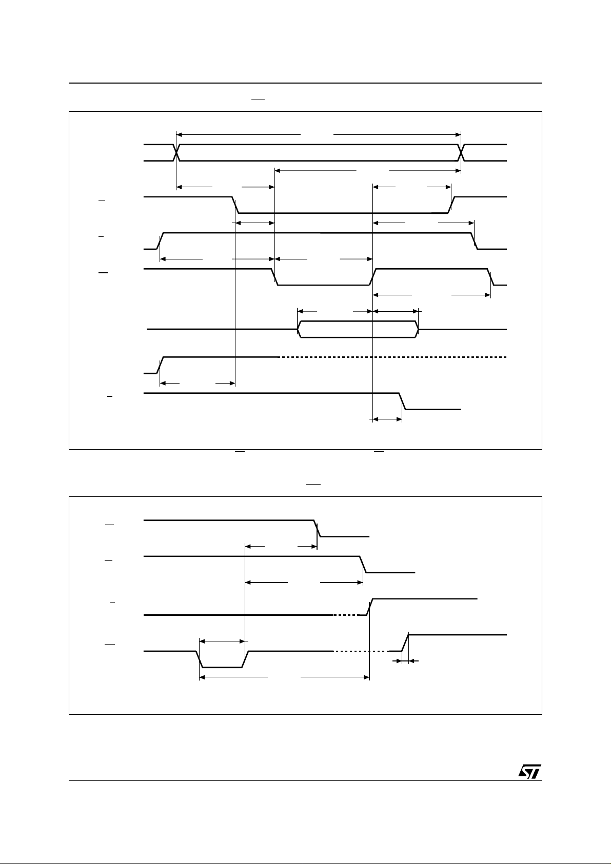
CH
t
WPH
t
AS
t
AH
t
VCSVCC
t
OEH
t
VIDR
t
RP
t
BUSY
t
RSP
Address Valid to Next Address Valid 100 120 ns
Chip Enable Low to Write Enable Low 0 0 ns
Write Enable Low to Write Enable High 50 50 ns
Input Valid to Write Enable High 50 50 ns
Write Enable High to Input Transition 0 0 ns
Write Enable High to Chip Enable High 0 0 ns
Write Enable High to Write Enable Low 30 30 ns
Address Valid to Write Enable Low 0 0 ns
Write Enable Low to Address Transition 50 50 ns
Output Enable High to Write Enable Low 0 0 ns
High to Chip Enable Low
Write Enable High to Output Enable Low 0 0 ns
RP Rise Time to V
ID
RP Pulse Width 500 500 ns
Program Erase Valid to RB Delay 90 90 ns
RP High to Write Enable Low 4 4 µs
100 120
Unit
= 30pF CL = 100pF
C
L
Min Max Min Max
50 50 µs
500 500 ns
19/36
Page 20

M36W108AT, M36W108AB
Figure 8. Flash Write AC Waveforms, W Controlled
tAVAV
A0-A19
tAVWL
EF
VALID
tWLAX
tWHEH
tELWL
G
tWLWHtGHWL
W
tDVWH
DQ0-DQ7
V
CCF
tVCHEL
RB
Note: Address are latched on the falling edge of W, Dat a i s l at ched on the rising edge of W.
VALID
tWHRL
tWHGL
tWHWL
tWHDX
AI02512
20/36
Page 21
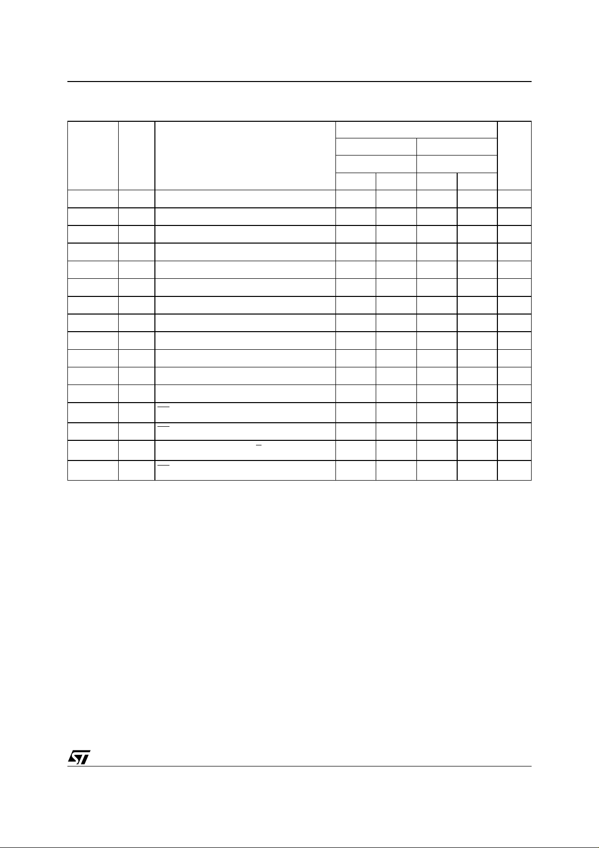
Table 20. Flash Write AC Characteristics, Chip Enable Controlled
(T
= 0 to 70 °C, –20 to 85 °C or –40 to 85 °C; V
A
= 2.7V to 3.6V)
CCF
M36W108AT, M36W108AB
Flash Memory Chip
Symbol Alt Parameter
t
AVAV
t
WLEL
t
ELEH
t
DVEH
t
EHDX
t
EHWH
t
EHEL
t
AVEL
t
ELAX
t
GHEL
t
VCHWL
t
EHGL
t
PHPHH
t
PLPX
t
EHRL
t
PHWL
Note: 1. Sampled only, not 100% tested.
2. This timing is for Temporary Block Unprotection operation.
(1,2)
(1)
(1)
t
WC
t
WS
t
CP
t
DS
t
DH
t
WH
t
CPH
t
AS
t
AH
t
VCSVCC
t
OEH
t
VIDR
t
RP
t
BUSY
t
RSP
Address Valid to Next Address Valid 100 120 ns
Write Enable Low to Chip Enable Low 0 0 ns
Chip Enable Low to Chip Enable High 50 50 ns
Input Valid to Chip Enable High 50 50 ns
Chip Enable High to Input Transition 0 0 ns
Chip Enable High to Write Enable High 0 0 ns
Chip Enable High to Chip Enable Low 30 20 ns
Address Valid to Chip Enable Low 0 0 ns
Chip Enable Low to Address Transition 50 50 ns
Output Enable High Chip Enable Low 0 0 ns
High to Write Enable Low
Chip Enable High to Output Enable Low 0 0 ns
RP Rise Time to V
ID
RP Pulse Width 500 500 ns
Program Erase Valid to RB Delay 90 90 ns
RP High to Write Enable Low 4 4 µs
100 120
Unit
= 30pF CL = 100pF
C
L
Min Max Min Max
50 50 µs
500 500 ns
21/36
Page 22
M36W108AT, M36W108AB
Figure 9. Flash Write AC Waveforms, EF Controlled
tAVAV
A0-A19
W
G
EF
DQ0-DQ7
V
CCF
RB
tVCHWL
tAVEL
tWLEL
VALID
tELEHtGHEL
tDVEH
VALID
tEHRL
tELAX
tEHWH
tEHGL
tEHEL
tEHDX
AI02513
Note: Address are latched on the falling edge of EF, Data is latched on the ri sing edge of EF.
Figure 10. Flash Read and Write AC Waveforms, RP Related
EF
tPHEL
W
tPHWL
RB
RP
tPLPX
tPLYH
tPHPHH
AI02514
22/36
Page 23

M36W108AT, M36W108AB
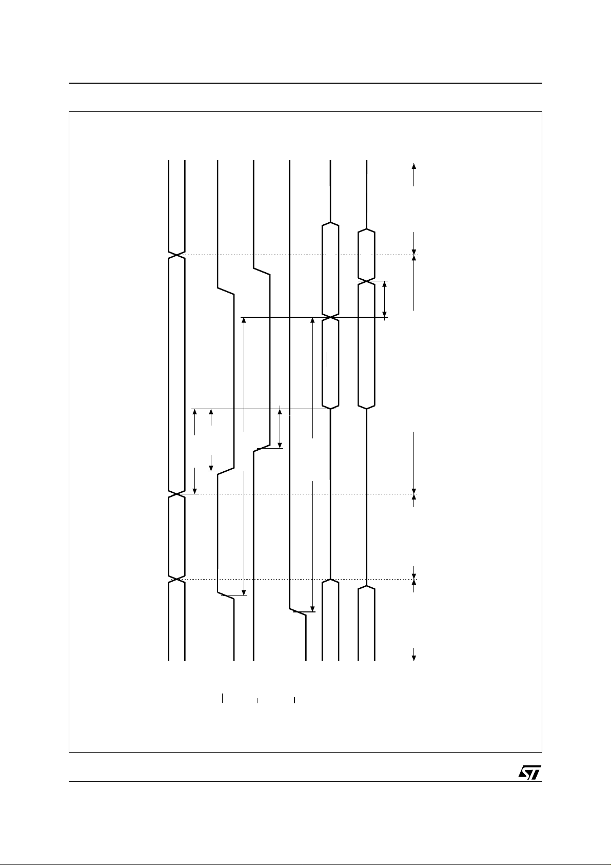
Table 21. Flash Data Polling and Toggle Bits AC Characteristics
(TA = 0 to 70 °C, –20 to 85 °C or –40 to 85 °C; V
Symbol Parameter
Write Enable High to DQ7 Valid (Program, W Controlled) 10 2400 10 2400 ms
t
WHQ7V
t
EHQ7V
t
Q7VQV
t
WHQV
t
EHQV
Note: 1. All other timings are defined in Read AC Characteristics table.
Write Enable High to DQ7 Valid (Chip Erase, W
Controlled)
Chip Enable High to DQ7 Valid (Program, EF Controlled) 10 2400 10 2400 µs
Chip Enable High to DQ7 Valid (Chip Erase, EF
Controlled)
Q7 Valid to Output Valid (Data Polling) 40 50 ns
Write Enable High to Output Valid (Program) 10 2400 10 2400 µs
Write Enable High to Output Valid (Chip Erase) 1.0 60 1.0 60 sec
Chip Enable High to Output Valid (Program) 10 2400 10 2400 µs
Chip Enable High to Output Valid (Chip Erase) 1.0 60 1.0 60 sec
= 2.7V to 3.6V)
CCF
= 30pF CL = 100pF
C
L
Min Max Min Max
1.0 60 1.0 60 sec
1.0 60 1.0 60 sec
(1)
Flash Memory Chip
100 120
Unit
23/36
Page 24
M36W108AT, M36W108AB
Figure 11. Flash Data Polling DQ7 AC Waveforms
AI02515B
ARRAY
READ CYCLE
ADDRESS (WITHIN BLOCKS)
tELQV
tAVQV
tEHQ7V
tGLQV
VALID
DQ7
tWHQ7V
VALID
tQ7VQV
IGNORE
DATA POLLING (LAST) CYCLE MEMORY
24/36
A0-A19
EF
READ CYCLES
DATA POLLING
PROGRAM
OR ERASE
CYCLE OF
LAST WRITE
G
W
DQ7
DQ0-DQ6
INSTRUCTION
Page 25
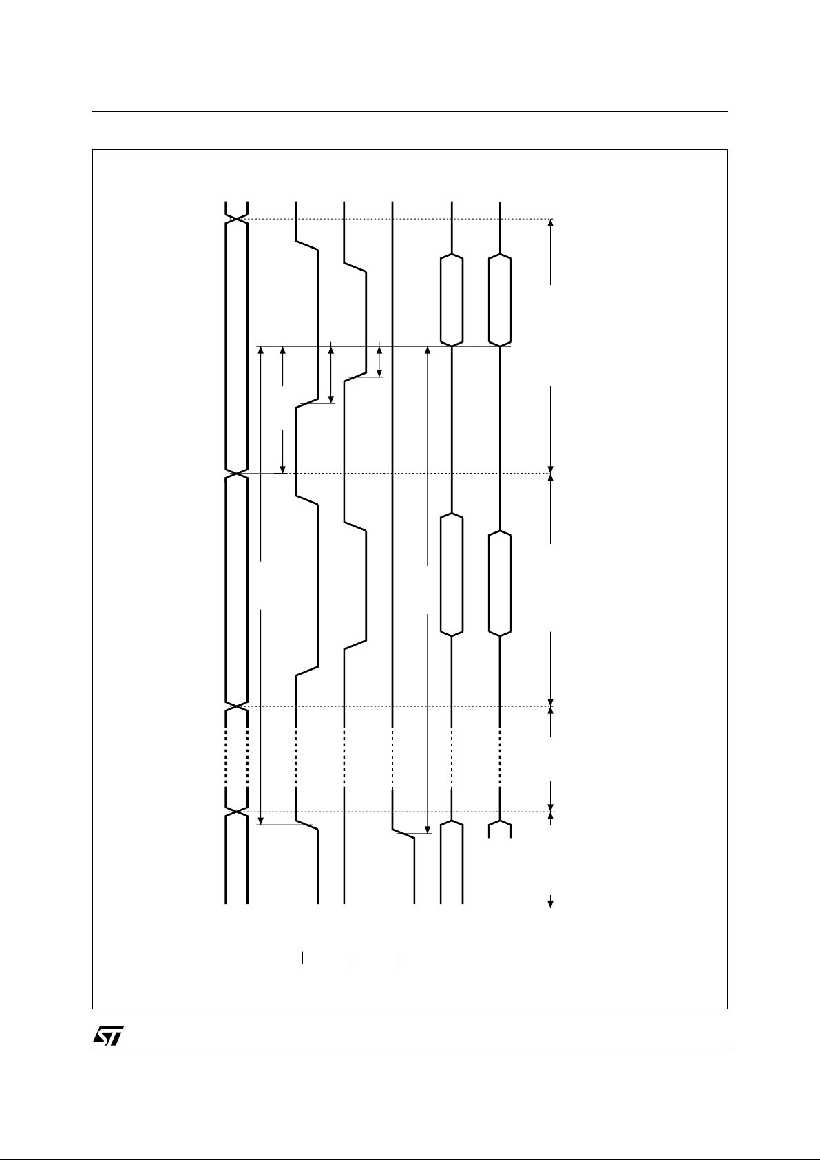
Figure 12. Flash Data Toggle DQ6, DQ2 AC Waveforms
M36W108AT, M36W108AB
AI02516
VALID
tAVQV
tEHQV
tELQV
tGLQV
VALID
tWHQV
STOP TOGGLE
VALID
IGNORE
READ CYCLE
MEMORY ARRAY
READ CYCLE
DATA TOGGLE
A0-A19
EF
DATA
TOGGLE
READ CYCLE
OF ERASE
PROGRAM
CYCLE OF
LAST WRITE
G
W
DQ6,DQ2
DQ0-DQ1,DQ3-DQ5,DQ7
INSTRUCTION
Note: All other timings are as a norm al Read cycle.
25/36
Page 26

M36W108AT, M36W108AB
Figure 13. Flash Data Polling Flowchart
START
READ DQ5 & DQ7
at VALID ADDRESS
DQ7
DATA
NO
DQ5
READ DQ7
DQ7
DATA
FAIL PASS
= 1
YES
=
NO
YES
YES
=
NO
Figure 14. Flash Data Toggle Flowchart
START
READ
DQ2, DQ5 & DQ6
DQ2, DQ6
=
TOGGLE
NO
DQ5
= 1
READ DQ2, DQ6
DQ2, DQ6
=
TOGGLE
FAIL PASS
NO
YES
YES
NO
YES
AI01369
AI01873
26/36
Page 27
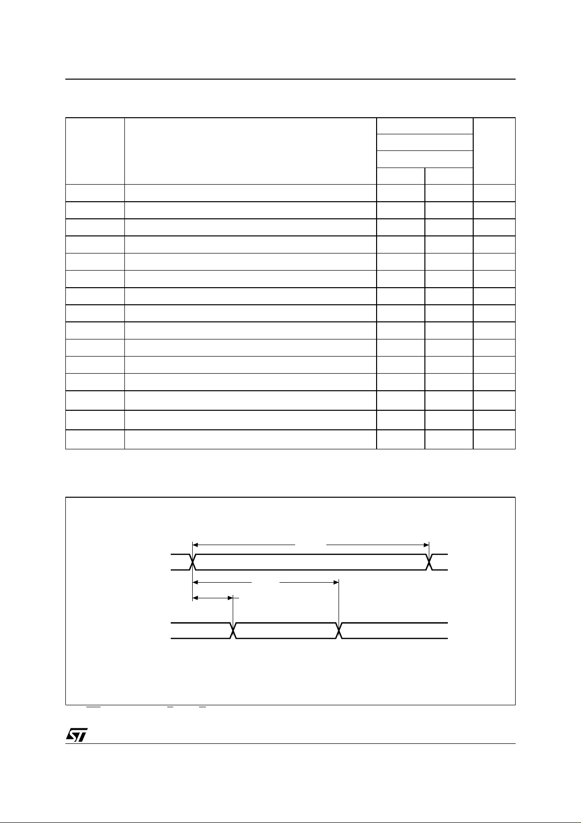
Table 22. SRAM Read AC Characteristics
(T
= 0 to 70 °C, –20 to 85 °C or –40 to 85 °C; V
A
= 2.7V to 3.6V)
CCS
M36W108AT, M36W108AB
SRAM Chip
Symbol Parameter
t
AVAV
t
AVQV
t
E1LQV
t
E2HQV
t
GLQV
t
E1LQX
t
E2HQX
t
GLQX
t
E1HQZ
t
E2LQZ
t
GHQZ
t
AXQX
(1)
t
PU
(1)
t
PD
t
CCR
Note: 1. Sampled only. Not 100% tested.
2. See Flash-SRAM Switching Waveforms.
Read Cycle Time 100 ns
Address Valid to Output Valid 100 ns
Chip Enable 1 Low to Output Valid 100 ns
Chip Enable 2 High to Output Valid 100 ns
Output Enable Low to Output Valid 50 ns
Chip Enable 1 Low to Output Transition 10 ns
Chip Enable 2 High to Output Transition 10 ns
Output Enable Low to Output Transition 5 ns
Chip Enable 1 High to Output Hi-Z 0 30 ns
Chip Enable 2 Low to Output Hi-Z 0 30 ns
Output Enable High to Output Hi-Z 0 30 ns
Address Transition to Output Transition 15 ns
Chip Enable 1 Low or Chip Enable 2 High to Power Up 0 ns
Chip Enable 1 High or Chip Enable 2 Low to Power Down 100 ns
(2)
Chip Enable Recovery Time 0 ns
100
= 100pF
C
L
Min Max
Unit
Figure 15. SRAM Read Mode AC Waveforms, Address Controlled
tAVAV
A0-A16
tAVQV
tAXQX
DQ0-DQ7
Note: E1S = Low, E2 S = High, G = Low, W = High.
VALID
DATA VALIDDATA VALID
AI02436
27/36
Page 28

M36W108AT, M36W108AB
Figure 16. SRAM Read AC Waveforms, E1S, E2S or G Controlled
tAVAV
A0-A16
E1S
E2S
G
DQ0-DQ7
Note: Write Enable (W) = High.
VALID
tAVQV tAXQX
tE1LQV
tE1LQX
tE2HQV
tE2HQX
tGLQX
tGLQV
tGHQZ
DATA VALID
tE1HQZ
tE2LQZ
AI02435
Figure 17. SRAM Stand-by AC Waveforms
E1S
E2S
tPU
50%
28/36
I
CC4
I
CC5
tPD
AI02517
Page 29

Table 23. SRAM Write AC Characteristics
(T
= 0 to 70 °C, –20 to 85 °C or –40 to 85 °C; V
A
= 2.7V to 3.6V)
CCS
M36W108AT, M36W108AB
SRAM Chip
Symbol Parameter
t
AVAV
t
AVWL
t
AVWH
t
WLWH
t
WHAX
t
WHDX
t
WHQX
t
WLQZ
t
AVE1L
t
AVE2H
t
E1HAX
t
E2LAX
t
DVWH
t
DVE1H
t
DVE2L
Write Cycle Time 100 ns
Address Valid to Write Enable Low 0 ns
Address Valid to Write Enable High 80 ns
Write Enable Pulse Width 70 ns
Write Enable High to Address Transition 0 ns
Write Enable High to Input Transition 0 ns
Write Enable High to Output Transition 0 ns
Write Enable Low to Output Hi-Z 0 30 ns
Address Valid to Chip Enable 1 Low 0 ns
Address Valid to Chip Enable 2 High 0 ns
Chip Enable 1 High to Address Transition 0 ns
Chip Enable 2 Low to Address Transition 0 ns
Input Valid to Write Enable High 40 ns
Input Valid to Chip Enable 1 High 40 ns
Input Valid to Chip Enable 2 Low 40 ns
100
= 100pF
C
L
Min Max
Unit
Figure 18. SRAM Write AC Waveforms, W Controlled
tAVAV
A0-A16
tAVE1L
E1S
tAVE2H
E2S
W
tWLQZ
DQ0-DQ7
Note: Output Enable (G) = Low.
VALID
tAVWH
tWLWHtAVWL
tDVWH
INPUT VALID
tWHAX
tWHQX
tWHDX
AI02434
29/36
Page 30

M36W108AT, M36W108AB
Figure 19. SRAM Write AC Waveforms, E1S Controlled
tAVAV
A0-A16
tAVE1L
E1S
E2S
tAVWL
W
DQ0-DQ7
Note: Output Enable (G) = High.
VALID
Figure 20. SRAM Write AC Waveforms, E2S Controlled
tDVE1H
tE1HAX
tWHDX
INPUT VALID
AI02433
A0-A16
E1S
E2S
W
DQ0-DQ7
Note: Output Enable (G) = High.
30/36
tAVE2H
tAVWL
tAVAV
VALID
tDVE2L
INPUT VALID
tE2LAX
tWHDX
AI02432
Page 31
M36W108AT, M36W108AB
Table 24. SRAM Low VCC Data Retention Characteristics
(T
= 0 to 70 °C; V
A
= 2.7 V to 3.6 V)
CCS
(1, 2)
Symbol Parameter Test Condition Min Max Unit
I
CCDR
V
DR
t
CDR
t
R
Note: 1. All other Inputs VIH ≤ VCC – 0.2V or VIL ≤ 0.2V.
2. Sampled only. Not 100% tested.
Supply Current (Data Retention)
Supply Voltage (Data Retention)
Chip Disable to Power Down
Operation Recovery Time 5 ms
CCS
E2S ≥ V
E1S
≥ V
E1S
≥ V
= 3V, E1S ≥ V
– 0.2V or E2S ≤ 0.2V, f = 0
CCS
– 0.2V,E2S ≤ 0.2V, f = 0
CCS
– 0.2V,E2S ≤ 0.2V, f = 0
CCS
CCS
– 0.2V,
20 µA
23.6V
0ns
V
Figure 21. SRAM Low VCC Data Retention AC Waveforms, E1S Contr ol led
V
tCDR
CCS
2.7 V
2.2 V
tRDATA RETENTION MODE
E1S
V
DR
E1S ≥ V
V
SS
CCS
– 0.2V
AI02438
31/36
Page 32

M36W108AT, M36W108AB
Figure 22. SRAM Low VCC Data Retention AC Waveforms, E2S Controlled
V
CCS
2.7 V
E2S
tCDR
V
DR
0.4 V
V
SS
Figure 23. Fl as h - SRAM Switc hi ng W aveforms
EF
E1S
DATA RETENTION MODE
tR
E2S ≤ 0.2V
AI02437
tCCRtCCR
32/36
E2S
AI02510
Page 33

M36W108AT, M36W108AB
Table 25. Ordering Information Scheme
Example: M36W108AT 100 ZM 1 T
Product Family
M36 = MMP (Flash + SRAM)
Operating Voltage
W = 2.7V to 3.6V
SRAM Chip size & organization
1 = 1 Mbit (x8)
Flash Chip size & orgnization
08A = 8 Mbit (x8)
Array Matrix
T = Top Boot
B = Bottom Boot
Speed
100 = 100 ns
120 = 120 ns
Package
ZM = LBGA48: 1mm pitch
ZN = LGA48: 1mm pitch
Temperature Range
1 = 0 to 70 °C
5 = –20 to 85 °C
6 = –40 to 85 °C
Option
T = Tape & Reel Packing
For a list of available options (Speed, Pac kage, etc...) or for furthe r information on any aspect of this device, please contact the ST Sales Office nearest to you.
33/36
Page 34

M36W108AT, M36W108AB
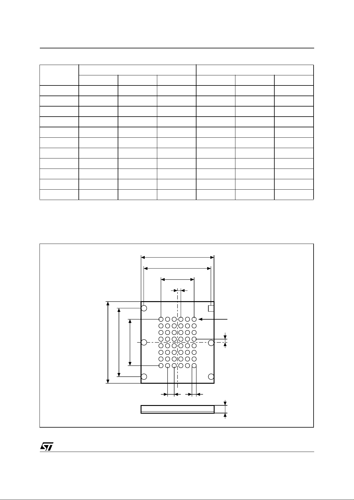
Table 26. LBGA48 - 6 x 8 balls, 1.0 mm pitch, Package Mechanical Data
Symb
Typ Min Max Typ Min Max
A 1.250 1.150 1.35 0 0.049 0. 045 0.053
A1 0.300 0.250 0.350 0.0 12 0.010 0.014
A2 0.950 – – 0.037 – –
b 0 .400 0.350 0.450 0.016 0.014 0 .018
ddd 0.150 0.006
D 10.000 9.800 10.200 0.394 0.386 0.402
D1 5.000 – – 0.197 – –
e 1 .000 – – 0.039 – –
E 12.000 11.800 12.2 00 0.472 0.465 0.480
E1 7.000 – – 0.276 – –
SD 0 .500 – – 0.020 – –
SE 0.500 – – 0.020 – –
mm inches
Figure 24. LBGA48 - 6 x 8 balls, 1.0 mm pitch, Package Outline
D
D1
SD
BALL "A1"
E1E
eb
A
SE
A1
ddd
A2
BGA-Z01
Drawing is not to scale.
34/36
Page 35
M36W108AT, M36W108AB
Table 27. LGA48 - 6 x 8 balls, 1.0 mm pitch, Package Mechanical Data
Symb
Typ Min Max Typ Min Max
A 0.950 0.900 1.000 0.037 0.035 0.039
b 0. 450 0.420 0.480 0.01 8 0.017 0.019
D 10.000 9 .800 10.200 0.394 0.386 0.402
D1 5.000 – – 0.197 – –
D2 9.200 – – 0.362 – –
e 1. 000 – – 0.039 – –
E 12.000 11.800 12.20 0 0.472 0.465 0.480
E1 7.000 – – 0.276 – –
E2 10.200 – – 0.402 – –
SD 0. 500 – – 0.020 – –
SE 0.500 – – 0.020 – –
mm inches
Figure 25. LGA48 - 6 x 8 balls, 1.0 mm pitch, Package Outline
D
D2
D1
SD
E
E1E2
eb
LAND "A1"
SE
A
Drawing is not to scale.
LGA-Z02
35/36
Page 36

M36W108AT, M36W108AB
Information furnished is believed to be ac curate and reli able. Howev er, STMicroel ectronics assumes no responsibilit y for the consequence s
of use of such information nor for any infringement of patents or other rights of third parties which may result from its use. No license is granted
by implic ation or otherwise under any patent or patent rights of STMi croelectr onics. Specifications mentioned in thi s publicati on are subject
to change without notice. This publication supersedes and replaces all information previously supplied. STMicroelectronics products are not
authorized for use as cri tical comp onents in life support dev i ces or systems wi t hout express written ap proval of STMi croelect ro nics.
The ST log o i s registered trademark of STMicroelectronics
1999 ST Microele ctronics - All Rights Re served
All other names are the property of their respective owners.
Australi a - Brazil - Canada - China - F rance - Germ any - Italy - Japan - Korea - M al aysia - Malt a - M exico - Morocco - The Net herlands -
Singapor e - Spain - Sweden - Switzerl and - Taiwan - Thailand - United Kingdom - U.S. A.
STMicroelect ro n ics GRO UP OF COMPANI ES
http://www.st.com
36/36
 Loading...