

Page 1

32 Mbit (2Mb x16, Dual Bank, Page) Flash Memory
and 4 Mbit (256K x16) SRAM, Multiple Memory Product
FEATURES SUMMARY
■ SUPPLY VOLTAGE
–V
DDF=VDDS
–V
■ ACCE SS TIME: 100,120ns
■ LOW POWE R CONSUMPT ION
■ ELECTRONIC SIGNATURE
= 12V for Fast Program (optional)
PPF
– Manufacturer Code: 20h
– Top Device Code, M36DR432A: 00A0h
– Bottom Device Code, M36DR432B: 00A1h
FLASH MEMORY
■ 32 Mbit (2Mb x16) BOOT BLOCK
– Parameter Blocks (Top or Bottom Location)
■ PROGRAMMING TIME
– 10µs typical
– Double Word Programming Option
■ ASYNCRONOUS PAGE MODE READ
– Page width: 4 Word
– Page Mode Access Time: 35ns
■ DUAL BANK OPERATION
– Read within o ne Bank while Program or
Erase within the other
– No Delay between Read and Write
Operations
■ BLOCK PROTECTION ON ALL BLOCKS
–WPF
■ COMMON FLASH INTERFACE
for Block Locking
– 64 bi t Security Code
SRAM
■ 4 Mbit (256K x 16 bit)
■ LOW V
■ POWER DOWN FEATURES USING TWO
DDS
CHIP ENABLE INPUTS
=1.65V to 2.2V
DATA RETENTION: 1V
M36DR432A
M36DR432B
Figure 1. Packages
FBGA
Stacked LFBGA66 (ZA)
8 x 8 ball array
1/46November 2001
Page 2
M36DR432A, M36DR432B
DESCRIPTION
The M36DR432 is a multichip memory device containing a 32 Mbit boot block Flash memory and a
4MbitofSRAM.ThedeviceisofferedinaStacked
LFBGA66 (0.8 mm pitch) package.
Thetwo components are distinguished by use with
three chip enable inputs: EF
and, E1S
and E2S for t he SRAM. The two components are also separately power supplied and
grounded.
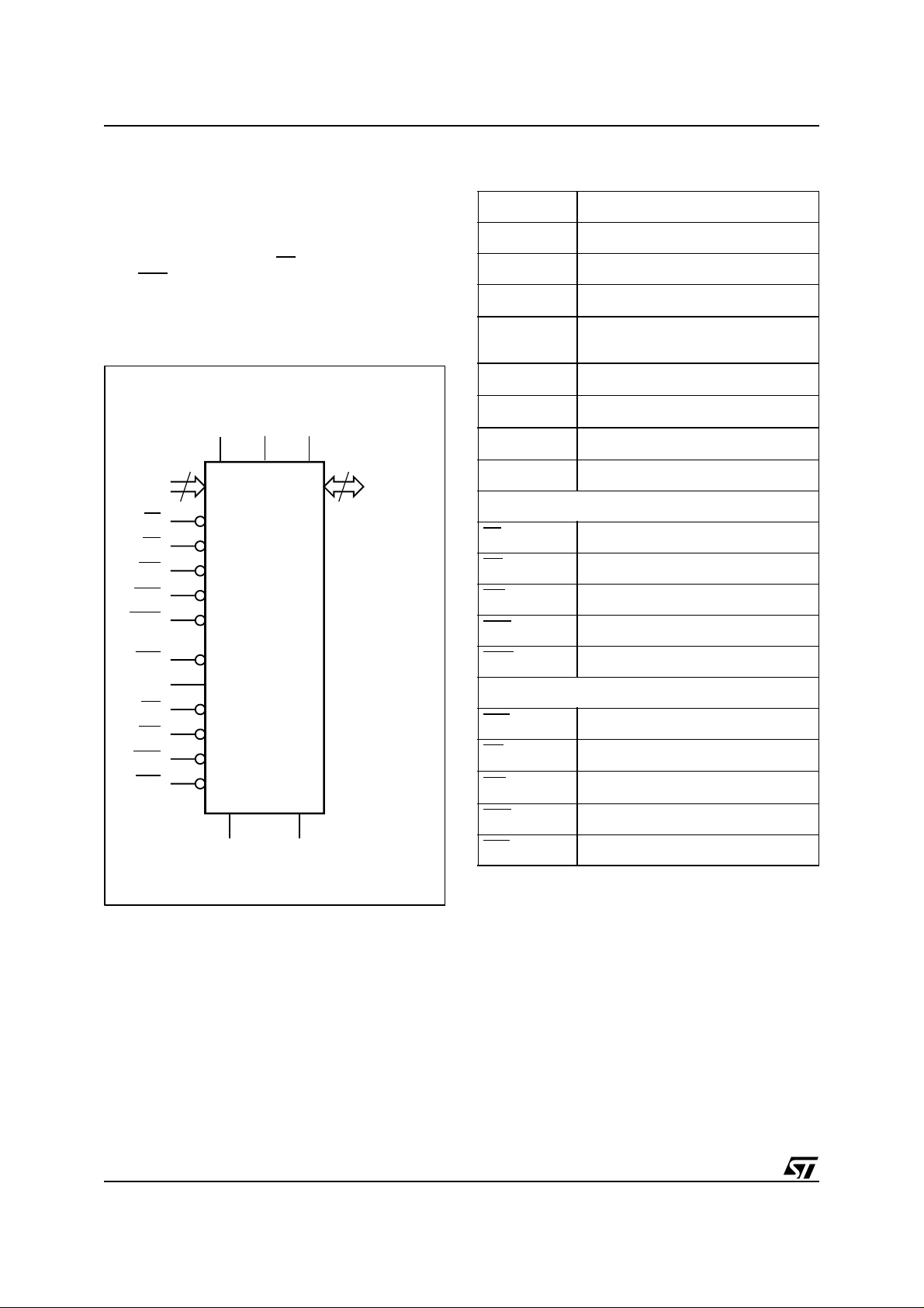
Figure 2. Logic Diagram
forthe Flash memory
Table 1. Signal Names
A0-A17 Address Inputs
A18-A20 Address Inputs for Flash Chip only
DQ0-DQ15 Data Input/Output
V
V
V
DDF
PPF
SSF
Flash Power Supply
Flash Optional Supply Voltage for Fast
Program & Erase
Flash Ground
A0-A20
EF
GF
WF
RPF
WPF
E1S
E2S
GS
WS
UBS
LBS
21
V
DDF
M36DR432A
M36DR432B
V
SSF
V
PPF
V
V
DDS
SSS
16
DQ0-DQ15
AI90203
V
DDS
V
SSS
NC Not Connected Internally
Flash control functions
EF
GF
WF
RPF
WPF
SRAM control functions
, E2S Chip Enable input
E1S
GS
WS
UBS
LBS
SRAM Power Supply
SRAM Ground
Chip Enable input
Output Enable input
Write Enable input
Reset input
Write Protect input
Output Enable input
Write Enable input
Upper Byte Enable input
Lower Byte Enable input
2/46
Page 3
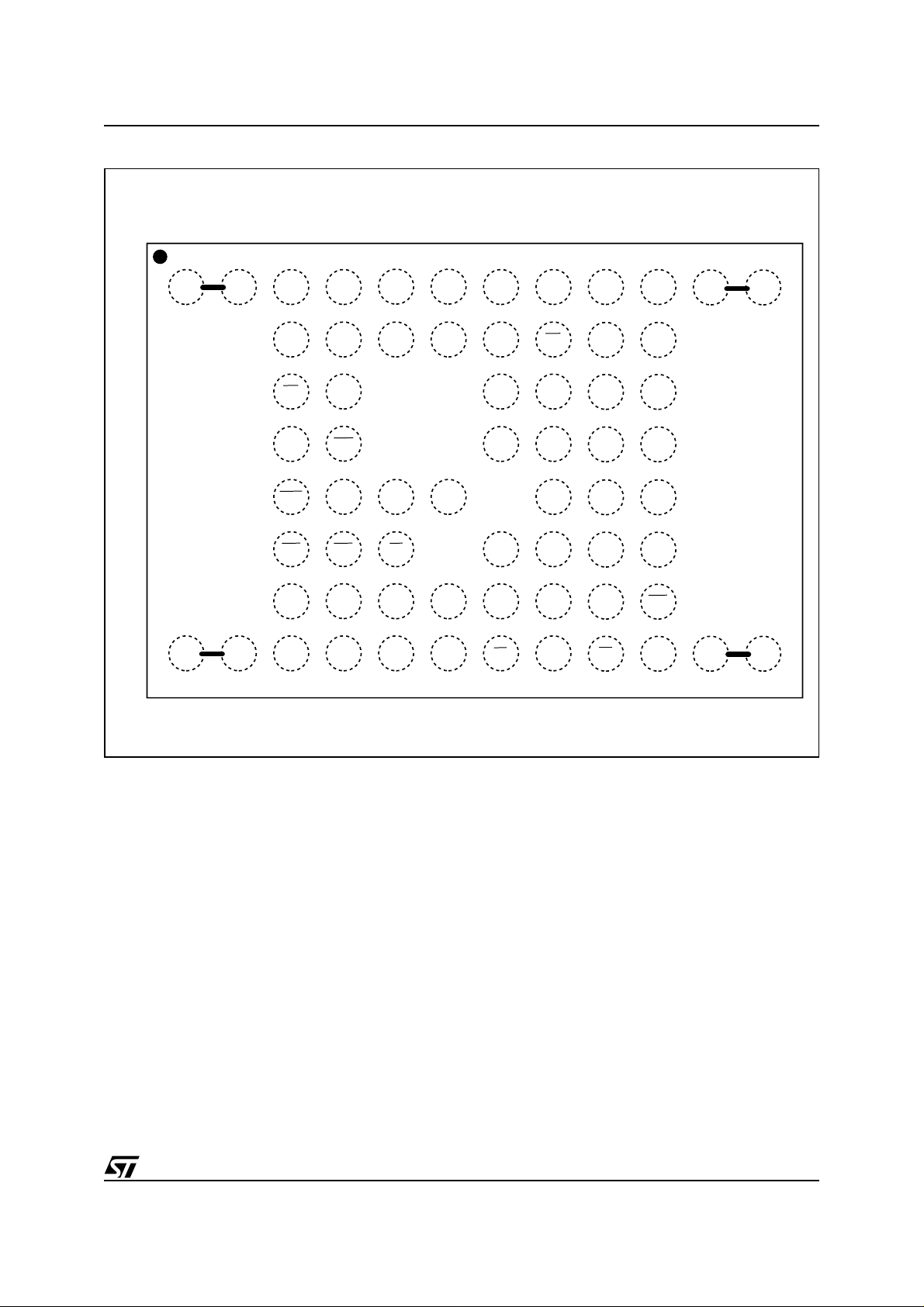
Figure 3. LFBGA Connections (Top view through package)
M36DR432A, M36DR432B
#2#1
A
B
C
D
E
F
G
H
SSS
NC V
A8 A10
RPF
V
PPF
UBS
A17
A5
A15 A14
DQ11A19WPF
A13A11A20NCNC
DQ15A9A16
DQ9GSLBS
EFA0A4NCNC
A12
WS
DQ6DQ13NCWF
E2SDQ12V
DQ10
DQ8
A2A3A6A7A18
SSF
V
SSF
DQ14
DQ4
V
DDS
DQ7
DQ5
V
DQ3DQ2
DQ1DQ0
E1SA1
87654321
NC
DDF
NCNCGF
#4#3
NCNC
NC
AI90204
3/46
Page 4
M36DR432A, M36DR432B
Table 2. Absolute Maximum Ratings
(1)
Symbol Parameter Value Unit
T
A
T
BIAS
T
STG
(2)
V
IO
V
DDF
V
DDS
V
PPF
Note: 1. Except for the rating "Operating Temperature Range", stresses above those listed in the Table "Absolute Maximum Ratings" may
cause permanent damage to the device. These are stress ratings only and operation of the device at these or any other conditions
above those indicated in the Operating sections of t his specification is not implied. Exposure to Absolute Ma ximu m Rating conditionsf or extendedperiods mayaffect devicereliability. Referalso tothe STMicroelectronics SUREProgram andother relevantquality documents.
2. Minimum voltage may undershoot to –2V during transition and for less than 20ns.
3. Depends on range.
4. V
DD=VDDS=VDDF
Ambient Operating Temperature
Temperature Under Bias –40 to 125 °C
Storage Temperature –55 to 150 °C
Input or Output Voltage
Flash Chip Supply Voltage –0.5 to 2.7 V
SRAM Chip Supply Voltage –0.2 to 2.6 V
Program Voltage –0.5 to 13.0 V
.
(3)
–40 to 85 °C
–0.2 to V
DD
(4)
+0.3
V
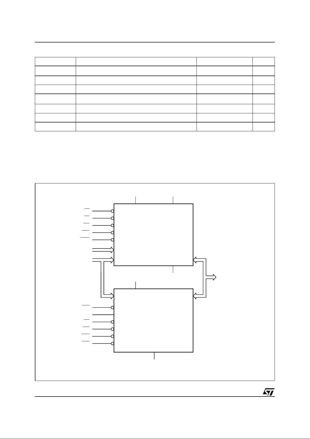
Figure 4. Functional Block Diagram
V
DDF
V
PPF
EF
GF
WF
RPF
WPF
A18-A20
A0-A17
E1S
E2S
GS
WS
UBS
LBS
Flash Memory
32 Mbit (x16)
V
DDS
SRAM
4 Mbit (x16)
V
SSF
DQ0-DQ15
4/46
V
SSS
AI90205
Page 5

SIGNAL DESCRIPTIONS
See Figure 2 and Table 1.
Address Inputs (A0-A17). Addresses A0 to A17
are common inputs for the Flas h chip and the
SRAM chip. The address inputs for the Flash
memory are latched during a write operation on
the falling edge of the Flash Chip Enable (EF
Write Enable ( WF
), while address inputs fo r the
)or
SRAM array are latched during a w rite operation
on the falling edge of the SRAM Chip Enable lines
or E2S ) or Write Enable (WS).
(E1S
Address Inputs (A18-A20). Addres s A18 to A 20
are address inputs for the Flash chip. They are
latched during a write operation on the falling edge
of Fl as h Ch ip Ena ble (EF
) or Write Enable (WF).
Data Input/Outputs (DQ0-DQ15). The input is
data to b e programmed in the Flash or SRAM
memory array or a comm and to be written to the
C.I. of the Flash chip. Both are latched on the rising edge of Flash Chip Enable (EF
able (W F
E2S) or Write Enable (WS
) and, SRAM Chip Enable lines (E1S or
). The output is data
)orWriteEn-
from the Flash memory or SRAM array, the Electronic Signature Manufacturer or Device codes or
the Status register Data Polling bit DQ7, the Toggle Bits D Q6 and DQ2, the Error bit DQ5 or the
Erase Timer bit DQ3. Outputs are valid when
Flash Chip Enable (EF
SRAM Chip Enable lines (E1S
Enable (GS
) are active. The output is high imped-
) and Output Enable (GF)or
or E2S) and Output
ance when the both the Flash chip and the SRAM
chip are deselected or the outputs are disabled
and when Reset (RPF
Flash Chip Enabl e (EF
)isataVIL.
). The Chip Enable input
for Flash activates the memory control logic, input
buffers, decoders and sense amplifiers. EF
at V
IH
deselects the memory and reduces the power consumption to the standby level and output do Hi-Z.
canalsobeusedtocontrolwritingtothecom-
EF
mand register and to the Flash memory array,
while WF
remains at VIL.ItisnotallowedtosetEF
at VIL,E1Sat VILand E2S at VIHat the same time.
Flash Write Enable (WF
). The Write Enable in-
put controls writing to the Command Register of
theFlashchipandAddress/Datalatches.Dataare
latched on the rising edge of WF
Flash Output Enable (GF
.
). The Output Enable
gates the outputs through the data buffers during
a read operation of the Flash chip. When GF
WF
are High the outpu ts are High impedance.
Flash Reset/Power Down Input (RPF
). The RPF
and
input provides hardware reset of the memory
(without affecting the Configuration Register status), and/or Power Down fun ctions, depending on
the Configuration Regis ter status. Reset/Power
Down of the memory is achieved by pulling RPF
V
for at least t
IL
. When the reset pulse is giv-
PLPH
to
M36DR432A, M36DR432B
en, if the memory is in Read, Erase Suspend Read
or Standby, it will output new valid dat a in t
after the rising edge of RPF.Ifthememoryisin
Erase or Program modes, the operation wi ll be
aborted and the res et recovery will take a maximum of t
Power Down (when enabled) in t
rising edge of RPF
. The mem ory will recover from
PLQ7V
PHQ7V2
. See Tables 1, 26 and Figure
11.
Flash Write Protect (WPF
). Write Protect is an
input to prot ect or unprotect the two lockable parameter blocks of the Flash memory. When WPF
is at VIL, the lock able blocks are protected. P r ogram or erase operations are not achievable.
When WPF
is at VIH, the lockable blocks are unprotected and they can be programmed or erased
(refer to Table 17).
SRAM Chip Enable (E1S
,E2S). The Chip En-
able input s for SRAM activate the mem ory control
logic, input buffers and decoders. E1S
E2S at V
deselects the me mory and reduces the
IL
power consumption to the standby level. E1S
E2S can also be used to control writing to the
SRAM memory array, while WS
is not al lowed to s et EF
at th e same time.
at V
IH
SRAMWriteEnable(WS
at VIL,E1Sat VILand E2S
). The Write Enable in-
remains at VIL.It
put cont ro ls writing to the SR A M m emory array.
WS
is active low.
SRAM Output Enable (GS
). T he Output Enable
gates the outputs through the data buffers during
a read operation of the SRAM chip. GS
low.
SRAM Upper Byte Enable (UBS
). Enable the
upper bytes for SRAM (DQ8-DQ 15). UBS
low.
SRAM Lower Byte Enable (LBS
). Enable the
lower bytes for SRAM (DQ0-DQ 7). LBS
low.
Supply Voltage(1.65 Vto 2.2V). Flash memo-
V
DDF
ry power supply for all operations (Read, Program and
Erase).
Programming Voltage (11.4V to 12.6V).
V
PPF
Used to provide high v oltage for f as t factory programming. High voltage on V
pin is required to
PPF
use the Double Word Program instruction. It is
also possible to perform word prog ram or erase instructions with V
Supply Voltage (1.65V to 2.2V). SRAM
V
DDS
pin grounded.
PPF
power supply for all operation s (Read, Prog ram).
V
SSF
and V
Ground. V
SSS
SSF
and V
reference for all v olt age measurements respectively in the Flash and SRAM chips.
PHQ7V1
after the
at VIHor
is active
isactive
is active
are the
SSS
and
5/46
Page 6
M36DR432A, M36DR432B
Table 3. Main Operation Modes
Operation
Mode
Read
Write
Block
Locking
Standby
Flash Memory
Reset X X X
Output
Disable
Read Flash must be disabled
Write Flash must be disabled
Standby/
Power
Down
SRAM
Data
Retention
Output
Disable
Note: X = VILor VIH,V
1. If UBS
and LBS are tied together the bus is at 16 bit. For an 8 bit bus configuration use UBS andLBS separately.
GF WF RPF WPF
EF
V
ILVILVIHVIH
V
ILVIHVILVIH
V
IL
V
IH
XX
XX
V
V
V
V
ILVIHVIHVIH
Any Flash mode is allowable
Any Flash mode is allowable
Any Flash mode is allowable
=12V±5%.
PPFH
V
PPF
E1S E2S GS WS
UBS,LBS
X Don't care SRAM must be disabled
V
or
V
IH
V
IH
IL
X Don't care Any SRAM mode is allowable Hi-Z
IH
X Don't care Any SRAM mode is allowable Hi-Z
IL
CCF
V
PPFH
SRAM must be disabled Data Input
Don't care SRAM must be disabled X
X Don't care Any SRAM mode is allowable Hi-Z
V
ILVIHVILVIH
V
ILVIHVIHVIL
V
XXX X Hi-Z
IH
V
X
X X X Hi-Z
IL
XXXX
V
XXX X Hi-Z
IH
V
X
X X X Hi-Z
IL
XXXX
V
ILVIHVIHVIH
V
IL
V
IL
V
IH
V
IH
X Hi-Z
(1)
DQ15-DQ0
Data
Output
Data out
Word Read
Data in
Word Write
Hi-Z
Hi-Z
6/46
Page 7

FLASH M EMO RY COMPONENT
Organization
The Flash Chip is organized as 2Mb x16 bits. A0A20 are the address lines, DQ0-DQ15 are the
Data Input/Output. Memory control is provided by
Chip Enable EF
able W F
Reset RPF
, Output Enable GF and Write En-
inputs.
is used to reset all the mem ory circuitry
and to set the chip in power down mode if this
function is enabled by a p roper setting of the Configuration Register. Erase and Program operations
are controlled by an internal Program/Erase Controller (P/E.C.). Status Register data output on
DQ7 provides a DataPolling signal, DQ6 and DQ2
provide Toggle signals and DQ5 provides error bit
to indicate the state of the P/E.C operat ions.
Memory Blocks
The device features asymmetrically b locked architecture. The Flash Chip has an array of 71 blocks
and is divided into two bank s A and B, providing
Dual Bank operations. While programming or
erasing in Bank A, read operations are possible
into Bank B or vice versa. The memory also features an erase s us pend allowing to read or program in another block wi thin the sam e bank. Once
suspended t he erase can be resumed. The Bank
Size and Sectorization are summarized in Table 4.
Parameter Blocks are located at the top of the
memory address space for the T op version, and at
the bottom for the Bottom version. The memory
maps are shown in Tables 5, 6, 7 and 8.
The Program and Erase operations are m anaged
automatically by the P/E.C. Block protection
against Program or Erase provides additional data
security. All blocks are protected at Power Up. Instructions are provided to protect or unprotect any
block in the application. A second register locks
the protection status while WPF
is low (see Block
Locking description). The Reset command does
not af fect the configuration of unprotected blo cks
and the Configuration Re giste r status.
Device Operations
The following operations can be performed using
the appropriate bus cycles: Read Array (Random,
and Page Modes), Write command, Output Disable, Standby, Res et/Power Down and Block
Locking. See Table 9.
Read. Read operations are used to output the
contents of the Memory Array, the Electronic Signature, t he Status Reg ister, the CFI, the Block
Protection Status or the Configurat ion Register
status. Read operation of the memory array is performed in asynchronous page mode, that provides
fast access time. Data is internally read and stored
in a page buf fer. The page has a size of 4 words
M36DR432A, M36DR432B
and is ad dres se d by A0-A1 address inputs. Read
operations of the Electronic Signature, the Status
Register, the CFI, the Block Protection Status, the
Configuration Register status and the Security
Code are performed as single asynchronous read
cycles (Random Read). Both Chip Enable EF
Output Enable GF
must be at VILin order to read
the out put of the memory.
Write. Write operations are used to give Instruc-
tion Co mm ands to the memory or to latch I nput
Data to be programmed. A write operation is initiated when Chip Enable EF
and Write Enable WF
are a t VILwith Output Enable GF at VIH.Addresses are latched on the falling edge of W F
whichever occurs last. Commands and Input Data
are latched on th e rising edge of WF
or EF whichever occurs first. Noise pulses of less than 5ns typical on EF
,WFand GF signals do not st art a write
cycle.
Dual Bank Operations. The Dual Bank allows to
read data from one bank of memory while a program or erase operation is in progress in the other
bank of the memory. Read and Write cycles can
be initiated for simultaneous operat ions in different
banks w ithout any d elay. Status Register during
Program or Erase m ust be monit ored using an address w ithin t he bank b eing modified.
Output Disable. The data outpu ts are high impedance when t he Output Enable GF
Write Enable WF
at VIH.
is at VIHwith
Standby. The m emory is in standby when Chip
Enable EF
is at VIHand the P/E.C. is idle. The
power consumption is reduced to the standby level
and the out puts are high impedance, inde pendent
of t he Output Enable GF
or Write Enable WF in-
puts.
Automatic Standby. When in Read mode, after
150ns of bus inactivity and when CMO S levels are
driving the addresses, the chip automat ically enters a pseudo-s tan dby mode where c ons umption
is red uc ed to the CMOS standby value, while outputs still drive the bus.
Power Down. Th e memory is in Power Down
when the Configuration Register is s et for Power
Down and RPF
is a t VIL. The power consumption
is reduced to the Power Down level, and Outp uts
are in high impedance , independent of the Chip
Enable EF
, Output Enable GF or Write Enable WF
inputs.
Block Locking. Any combination of blocks can
be temporarily protected again st Program or
Erase by setting the lock register and pulling WPF
to VIL(see Block Lock instruction).
and
or EF
7/46
Page 8
M36DR432A, M36DR432B
Table4.BankSizeandSectorization
Bank Size Parameter Blocks Main Blocks
Bank A 4 Mbit 8 blocks of 4 KWord 7 blocks of 32 KWord
Bank B 28 Mbit - 56 blocks of 32 KWord
Table 5. Bank A, Top Boot Block Addresses
M36DR432A
#
0 4 1FF000h-1FFFFFh
1 4 1FE000h-1FEFFFh
2 4 1FD000h-1FDFFFh
3 4 1FC000h-1FCFFFh
4 4 1FB000h-1FBFFFh
5 4 1FA000h-1FAFFFh
6 4 1F9000h-1F9FFFh
7 4 1F8000h-1F8FFFh
8 32 1F0000h-1F7FFFh
9 32 1E8000h-1EFFFFh
10 32 1E0000h-1E7FFFh
11 32 1D8000h-1DFFFFh
12 32 1D0000h-1D7FFFh
13 32 1C8000h-1CFFFFh
14 32 1C0000h-1C7FFFh
Size
(KWord)
Address Range
Table 6. Bank B, Top Boot Block Addresses
M36DR432A
#
0 32 1B8000h-1BFFFFh
1 32 1B0000h-1B7FFFh
2 32 1A8000h-1AFFFFh
3 32 1A0000h-1A7FFFh
4 32 198000h-19FFFFh
5 32 190000h-197FFFh
6 32 188000h-18FFFFh
7 32 180000h-187FFFh
8 32 178000h-17FFFFh
9 32 170000h-177FFFh
10 32 168000h-16FFFFh
11 32 160000h-167FFFh
12 32 158000h-15FFFFh
13 32 150000h-157FFFh
14 32 148000h-14FFFFh
15 32 140000h-147FFFh
16 32 138000h-13FFFFh
Size
(KWord)
Address Range
17 32 130000h-137FFFh
18 32 128000h-12FFFFh
19 32 120000h-127FFFh
20 32 118000h-11FFFFh
21 32 110000h-117FFFh
22 32 108000h-10FFFFh
23 32 100000h-107FFFh
24 32 0F8000h-0FFFFFh
25 32 0F0000h-0F7FFFh
26 32 0E8000h-0EFFFFh
27 32 0E0000h-0E7FFFh
28 32 0D8000h-0DFFFFh
29 32 0D0000h-0D7FFFh
30 32 0C8000h-0CFFFFh
31 32 0C0000h-0C7FFFh
32 32 0B8000h-0BFFFFh
33 32 0B0000h-0B7FFFh
34 32 0A8000h-0AFFFFh
35 32 0A0000h-0A7FFFh
36 32 098000h-09FFFFh
37 32 090000h-097FFFh
38 32 088000h-08FFFFh
39 32 080000h-087FFFh
40 32 078000h-07FFFFh
41 32 070000h-077FFFh
42 32 068000h-06FFFFh
43 32 060000h-067FFFh
44 32 058000h-05FFFFh
45 32 050000h-057FFFh
46 32 048000h-04FFFFh
47 32 040000h-047FFFh
48 32 038000h-03FFFFh
49 32 030000h-037FFFh
50 32 028000h-02FFFFh
51 32 020000h-027FFFh
52 32 018000h-01FFFFh
53 32 010000h-017FFFh
54 32 008000h-00FFFFh
55 32 000000h-007FFFh
8/46
Page 9
M36DR432A, M36DR432B
Table7.BankB, Bottom BootBlockAddresses
M36DR432B
#
55 32 1F8000h-1FFFFFh
54 32 1F0000h-1F7FFFh
53 32 1E8000h-1EFFFFh
52 32 1E0000h-1E7FFFh
51 32 1D8000h-1DFFFFh
50 32 1D0000h-1D7FFFh
49 32 1C8000h-1CFFFFh
48 32 1C0000h-1C7FFFh
47 32 1B8000h-1BFFFFh
46 32 1B0000h-1B7FFFh
45 32 1A8000h-1AFFFFh
44 32 1A0000h-1A7FFFh
43 32 198000h-19FFFFh
42 32 190000h-197FFFh
41 32 188000h-18FFFFh
40 32 180000h-187FFFh
39 32 178000h-17FFFFh
38 32 170000h-177FFFh
37 32 168000h-16FFFFh
36 32 160000h-167FFFh
35 32 158000h-15FFFFh
34 32 150000h-157FFFh
33 32 148000h-14FFFFh
32 32 140000h-147FFFh
31 32 138000h-13FFFFh
30 32 130000h-137FFFh
29 32 128000h-12FFFFh
28 32 120000h-127FFFh
27 32 118000h-11FFFFh
26 32 110000h-117FFFh
25 32 108000h-10FFFFh
24 32 100000h-107FFFh
23 32 0F8000h-0FFFFFh
22 32 0F0000h-0F7FFFh
21 32 0E8000h-0EFFFFh
20 32 0E0000h-0E7FFFh
19 32 0D8000h-0DFFFFh
Size
(KWord)
Address Range
18 32 0D0000h-0D7FFFh
17 32 0C8000h-0CFFFFh
16 32 0C0000h-0C7FFFh
15 32 0B8000h-0BFFFFh
14 32 0B0000h-0B7FFFh
13 32 0A8000h-0AFFFFh
12 32 0A0000h-0A7FFFh
11 32 098000h-09FFFFh
10 32 090000h-097FFFh
9 32 088000h-08FFFFh
8 32 080000h-087FFFh
7 32 078000h-07FFFFh
6 32 070000h-077FFFh
5 32 068000h-06FFFFh
4 32 060000h-067FFFh
3 32 058000h-05FFFFh
2 32 050000h-057FFFh
1 32 048000h-04FFFFh
0 32 040000h-047FFFh
Table8.BankA, Bottom BootBlockAddresses
M36DR432B
#
14 32 038000h-03FFFFh
13 32 030000h-037FFFh
12 32 028000h-02FFFFh
11 32 020000h-027FFFh
10 32 018000h-01FFFFh
9 32 010000h-017FFFh
8 32 008000h-00FFFFh
7 4 007000h-007FFFh
6 4 006000h-006FFFh
5 4 005000h-005FFFh
4 4 004000h-004FFFh
3 4 003000h-003FFFh
2 4 002000h-002FFFh
1 4 001000h-001FFFh
0 4 000000h-000FFFh
Size
(KWord)
Address Range
9/46
Page 10
M36DR432A, M36DR432B
Table 9. User Bus Operations
(1)
Operation EF GF WF RPF WPF DQ0-DQ15
Write
Output Disable
Standby
V
IL
V
IL
V
IH
Reset / Power Down X X X
Block Locking
Note: 1. X = Don't care.
V
IL
V
IH
V
IH
V
IL
V
IH
XX
XX
V
IH
V
IH
V
IH
V
IL
V
IH
Table 10. Read Electronic Signature (AS and Read CFI instructions)
Code Device EF
Manufacturer Code
M36DR432A
Device Code
M36DR432B
GF WF A0 A1 A2-A7
V
V
V
IL
IL
V
V
IL
IL
V
V
IL
IL
IH
V
IHVIH
V
IHVIH
V
IL
V
V
V
0 Don't Care 20h 00h
IL
0 Don't Care A0h 00h
IL
0 Don't Care A1h 00h
IL
Table 11. Read Bl ock Protecti on (AS and Read CFI instructions)
Block Status EF
GF WF A0 A1 A2-A7
Other
Addresses
A12-A20 DQ0 DQ1 DQ2-DQ15
Other
Addresses
V
IH
V
IH
V
IH
V
IH
V
IL
Data Input
Hi-Z
Hi-Z
Hi-Z
X
DQ0-DQ7 DQ8-DQ15
Protected Block
Unprotected Block
Locked Block
V
ILVILVIHVILVIH
VILVILVIHVILV
V
ILVILVIHVILVIH
0 Don't Care Block Address 1 0 0000h
0 Don't Care Block Address 0 0 0000h
IH
0 Don't Care Block Address X 1 0000h
Table 12. Read Con f iguration Regi ster (AS and Read CFI instructions)
Function EF GF WF A0 A1 A2-A7 Other Addresses DQ10
RPF
V
V
V
V
Reset
Reset/Power Down
IL
IL
IH
V
V
IL
V
IL
IH
V
IH
V
V
IH
0 Don't Care 0 Don't Care
IH
0 Don't Care 1 Don't Care
IH
DQ0-DQ9
DQ11-DQ15
10/46
Page 11
INSTRUCTIONS AND COMMANDS
Seventeen instructions are def ined (s ee Table
15), and the internal P / E.C. automat icall y ha ndles
all timi ng and verification of the Program and
Erase operat ions. The Status Register Data Polling, Toggle, Error bits can be read at any time, during programming or erase, to monitor the progress
of t he operation.
Instructions, made up of one or more commands
writtenincycles,canbegiventotheProgram/
Erase Controller through a Command Interface
(C.I.). The C.I. latches commands written to the
memory. Commands are made o f address and
data sequences . Two Coded Cycles unlock the
Command Interface. They are followed by an input
command or a confirmation command. The Coded
Sequence consists of writing the data AAh at the
address 555h during the first cycle and the data
55h at the address 2AAh during the s ec ond cycle.
Instructions are composed of up to six cycles. The
first two cycles input a Coded Sequence to the
Command Interface which is common to all instructions (see Table 15). The third cycle inputs
the instruction set-up command. Subsequent cycles output the addressed data, Electronic Si gnature, Block Protection, C onfiguration Register
Status or CF I Query for Read operat ions. In order
to give additional data protection, the instructions
for Block Erase and Bank Eras e require further
command inputs. For a Program instruction, the
fourthcommandcycleinputs the ad dress and data
to be programmed. For a Double Word Programming instruction, the fourth and fifth command cycles input the address and data to be
programmed. For a Block Erase and Bank Erase
instructions, the fourth and fifth cycles input a further Coded Sequence before the Erase co nfirm
command on the sixth cycle. Any combination of
blocks of the same memory bank can be erased.
Erasure of a memory block may be suspended, in
order to read data from another block or to program data in another block, and then resumed.
When powerisfirst applied the command interface
is reset to Read Array.
Command sequencing must be followed exactly.
Any invalid combination of commands will reset
the device to Read Array. The inc re as ed number
of cycles has been chosen to ensure maximum
data security.
M36DR432A, M36DR432B
Table 13. Commands
Hex Code Command
00h Bypass Reset
10h Bank Erase Confirm
20h Unlock Bypass
30h Block Erase Resume/Confirm
40h Double Word Program
Block Protect, or
60h
80h Set-up Erase
90h
98h CFI Query
A0h Program
B0h Erase Suspend
F0h Read Array/Reset
Read/Reset (RD) I nstruction. The Read/Reset
instruction cons ists of one write cycle givin g the
command F0h. It can be optionally p receded by
the two Coded Cycles. Subsequent read operations will read the me mory array addressed and
output the data read.
CFI Query (RCFI) Instruction. Common Flash
Interface Query m ode is entered writing 98h at address 55h. The CFI data structure gives information on the device, such as the sectorization, the
command set and some electrical specifica tions.
Table 18, 19, 20 and 21 show the addresses used
to retr ieve each data. The CFI data structure contains also a security area; in this sect ion, a 64 bit
unique security number is written, starting at address 80h. This area can be accessed only in read
mode by the final user and there are no ways of
changing the code af te r it has been written by ST.
Write a read instruction (RD) to return to Read
mode.
Auto Select (AS) Instruction. This instruction uses
two Coded Cycles followed by one write cycle giving the command 90h to address 555h for command set-up. A subsequent read will outpu t the
Manufacturer or th e Device Code (Electronic Signature), the Block Protection status or the Configuration Register status depending on the levels of
A0 and A1 (see Table 10, 11 and 12). A7-A2 must
be at V
Block Unprotect, or
Block Lock, or
Write Configuration Register
Read Electronic Signature, or
Block Protection Status, or
Configuration Register Status
, while other address input are ignored.
IL
11/46
Page 12

M36DR432A, M36DR432B
The bank address is don’t care f or this instruction.
The Electronic Signature can be read from the
memory allowing program min g equipment or applications to automatic ally match their interfac e to
the characteristics of Flash Chip. The Manufac turer Code is output when the address lines A0 and
A1 are at V
is at V
, the Device Code is output when A0
IL
with A1 at VIL.
IH
The codes are output on DQ 0-DQ7 with DQ8DQ15 at 00h. The AS instruction also allows the
access to the Block Protection Status. After giving
the AS instru ction, A0 is s et to V
with A1 at VIH,
IL
while A12-A20 define the address of the block to
be verified. A read in these conditions will output a
01h if the block is p ro tected and a 00h if the block
is not protected.
The AS Instruction final ly allows the access to the
Configuration Register status if both A0 and A1
are s et to V
is active as RPF
. If DQ10 is '0' only the Reset function
IH
is set to VIL(default at power-up).
If DQ10 is '1' both the Reset and the Power Down
functions will be achieved by pulling RPF
to VIL.
The other bits of the Con figurati on Register are reserved and must be ignored. A reset command
puts t he dev ice in read array mode.
Write Configuration Register (CR) Instruction. Th is instruction uses two Code d Cycles fol-
lowed by one write cycle giving the command 60h
to address 555h. A further write cycle giving the
command 03h writes the contents of address bits
A0-A15 to the 16 bits configurat ion register. Bits
written by inputs A0-A9 and A11-A15 are reserved
for future use. Address input A10 defines the status of the Reset/Power Down functions. It mus t be
set to V
V
IH
to enable only the Reset function and to
IL
to enable also the Power Down function. At
Power Up all the Configuration Register bits are
reset to '0'.
Enter Bypass Mode (EBY) Instruction. This instruction uses the two Coded cycles followed by
one write cycle giving the command 20h to address 555h for mode set-up. Onc e in By pas s
mode, the device will accept the Exit Bypass
(XBY) and Program or Double Word Program in
Bypass mode (P GBY, DPGBY) comm ands. The
Bypass mode allows to reduce th e overall programming time when l arge memory arrays need to
be programmed.
Exit Bypass Mode (XBY) Instruction. This in-
struction uses t wo write cycles. The first inputs to
the memory the command 90h and the second inputs the Exit Bypass mode confirm (00h). After the
XBYinstruction, the device resetsto Read Memory Arra y mode.
Program in Bypass Mode (PGBY) Instruction. This instruction uses two write cycles. The
Program command A0h is written to any Address
on the first cycle and the second write cycle latch-
esthe A ddresson the falling edge of WF
or EF and
the Data to be written on t he rising edge and starts
the P/E.C. Read operations within the same bank
output the Status R egister bits af ter the program ming has started. Memory programming is m ade
only by writing '0' in place of '1'. Status bit s DQ6
and DQ7 determine if programming is on-going
and DQ5 allows verification of any possible error.
Program (PG) Instruction. This instruction uses
four write cycles. The Program command A0h is
written to address 555h on the t hird cycle after two
Coded Cycles. A fourth w rite operation latches the
Address and the Data to be written and starts t he
P/E.C. Read operations within the sam e bank output the Status Register bits after the programming
has sta rted. Memory programming is made only
by writing '0' in place of '1'. Status bits DQ6 and
DQ7 determine if programming is on-going and
DQ5 allows verification of any possible error. Programming at an address not in blocks being
erased is also possible during erase su spend.
Double Word Program (DPG) Instruction. This
feature is offered to improve the programming
throughput, writing a page of two adjacent words
in parall el. High voltage (11.4V to 12. 6V ) on V
PP
pin is required. This instruction uses five write cycles. The double word program command 40h is
written to address 555h on the t hird cycle after two
Coded Cycles. A fourth write c ycle latches the address and data t o be written to the first location. A
fifth write cycle latches the new data to be written
to the s ec ond location and starts the P/E.C.. Note
thatt he two locations must h av e the sam e address
except for the address bit A0. The Double Word
Program can be executed in Bypass mode (DP GBY) to skip the two coded cycles at the beginning
of each command.
Block Protect (BP), Block U nprotect (BU),
Block Lock (BL) Instructions. All blocks are
protected at power-up. Each block of the array has
two levels of prot ec tion against program or erase
operation. The first level is set by the Block Protect
instruction; a p rotect ed block cannot be programmed or erased until a Block Unprotect instruction is given for that block. A second level of
protection is set by the Block Lock instruction, and
requires the use of the WPF
pin, according to the
following scheme:
– when WPF
is at VIH, the Lock status is overridden and all blocks can be protected or unprotected;
– when WP F
is at VIL, Lock status is enabled; the
locked blocks are protected, regardless of their
previous protect state, and protection status
cannot be chan ged. Blocks that are not lock ed
can still change their protection status, and program or erase ac c ordingl y;
12/46
Page 13

M36DR432A, M36DR432B
– the loc k status is cleared for all blocks at power
up; once a block has been locked s tate can be
cleared only with a reset command. T he protection and lock status can be m onit ored for each
block using the Autoselect (A S) instruction. Protected blocks wil l output a ‘1’ on DQ0 and lock ed
blocks will out put a ‘1’ on DQ1.
Refer to Table 14 for a list of the protection state s.
Block Erase (BE) In struction. This instruction
uses a m inimum of six write cycles. The Erase
Set-up command 80h is written to address 555h
on third cycle after the two Coded cycles. The
Block Erase Confirm c ommand 30h is similarly
written on the sixth cycle after another two Coded
cycles and an address within the block to be
erased is given an d latched in to the memory.
Additional block Erase Confirm commands and
block addresses can be written subsequently to
erase other blocks in parallel, without further Coded cycles. All blocks must belong to the same
bank of memory; if a new block belongi ng to the
other bank is given, the operation is abort ed. The
erase will start a fter an erase timeout period of
100µs. Thus, additional Erase Confirm commands
for other blocks must be given within this delay.
The input of a new Erase Confirm c ommand will
restart the time out period. The status of the internal timer can be monitored through the level of
DQ3, if DQ3 is '0' the Block Erase Comm and has
been given and the timeout is running, if DQ3 is '1',
the timeout has expired an d the P/E.C. is erasing
the Block(s). If the second command given is not
an erase confirm or if the Coded cycles are wrong,
the instruction aborts, and the dev ice is reset to
Read Array. It is not necessary to program t he
block with 00h as the P/E.C. will do this automatically before erasing to FFh. Read operations within the same bank, after the sixth rising edge of WF
or EF, output the s tatus register bits.
During the execution of the erase by the P/E.C.,
the memory accepts only the Erase Susp end ES
instruction; the Read/Reset RD instruction is accepted during the 100µs time-out perio d. Data
Polling bit DQ7 returns '0' while the erasure is in
progress and '1' when it has completed. The Toggle bit DQ6 toggles during the erase operation,
and stops when erase is completed.
After completion the Status Register bit DQ5 returns '1' if there has been an erase f ailure. In such
a situat ion, the Toggle bit DQ2 can be used to determine which block is not correctly erased. In the
case of erase failure, a Read/Reset RD instruction
is nece ssary in order to reset the P /E.C.
Bank Erase (BKE) Instruction. This instruction
uses s ix w rite cycles and is used to erase all the
blocks belonging to t he s elected bank. The Er as e
Set-up command 80h is written to address 555h
on the third cycle after the two Coded cycles. T he
Bank Erase Confirm command 10h is similarly
written on the sixth cycle after another two Coded
cycles at an address within the selected bank . If
the second command given is not an erase confirm or if the Coded cycles are wrong, the instruction aborts a nd the device is reset to Read Array.
It is not necessary to program the array with 00h
first as the P/E.C. will automatically do this before
erasing it to FFh. Read operations within the same
bank after the sixth rising edge of WF
or EF output
the Status Register bits. During the execution of
the erase by the P/E.C., Data Polling bit DQ7 returns '0', then '1' on completion. The Toggle bit
DQ6 toggles during erase operation and stops
when erase is completed. A fter completion the
Status Register bit DQ5 returns '1' if there has
been an Erase Failure.
Erase Suspend (ES) Instruction. In a dual bank
memory the Erase Suspend instruction is used to
read data within the bank where erase is in
progress. It i s also possibl e to program data in
blocks not being erased.
The Erase Suspend instruction consists of writ ing
the command B0h without any specific address.
No Coded Cycles are required. Erase suspend is
accepted only during the Block Erase instruction
execution. The Toggle bit DQ6 stops toggling
when the P/ E.C. is suspended within 15µs after
the Eras e Suspend (ES) command has b een written. The device will then automatically be set t o
Read Memory Array mode. When erase is suspended, a Read from blocks being erased will output DQ2 toggling and DQ 6 at '1'. A Read from a
block not being erased returns valid data. During
suspension the memory will respond only to the
Erase Resume ER and the Program PG instructions. A Program operation can be initiated during
erase suspend in one of the blocks not being
erased. It will result in DQ6 toggling when the dat a
is be ing program med.
Erase Resume (ER) Instruction. If an Erase
Suspend instruction was previously executed, the
erase operation may be resumed by giving the
command 30h, at an address within the bank being eras ed and without an y Coded Cycle.
13/46
Page 14
M36DR432A, M36DR432B
Table 14. Pro t ecti on States
(2)
Current State
(WP, DQ1, DQ0)
Program/Erase
Allowed
(1)
Next State After Event
(3)
Protect Unprotect Lock WP transition
100 yes 101 100 111 000
101 no 101 100 111 001
110 yes 111 110 111 011
111 no 111 110 111 011
000 yes 001 000 011 100
001 no 001 000 011 101
011 no 011 011 011
Note: 1. All blocksare protectedat power-up, so the defaultconfigurationis 001 or 101 accordingto WPF status.
2. Current state and Next state gives the protection status of a block. The protection status is defined by the write protect pin and by
DQ1(=1foralockedblock)andDQ0(=1foraprotectedblock)asreadintheAutoselectinstructionwithA1=V
3. Next state is the protection status of a block after a Protect or Unprotect or Lock command has been issued or after WPF
changed its logic value.
4. A WPF
Table 15. Instructions
transition to VIHon a locked block will restore the previous DQ0 value, giving a 111 or 110.
(1,2)
111 or 110
andA0=VIL.
IH
Mne. Instr. Cyc. 1st Cyc. 2nd Cyc. 3rd Cyc. 4th Cyc. 5th Cyc. 6th Cyc.
RD
Read/Reset
(4)
Memory Array
(3)
Addr.
1+
Data F0h
Addr. 555h 2AAh 555h
3+
Data AAh 55h F0h
X
Read Memory Array until a new write cycle is initiated.
Read Memory Array until a new
write cycle is initiated.
Addr. 55h
RCFI CFI Query 1+
Read CFI data until a new write cycle is initiated.
Data 98h
Addr. 555h 2AAh 555h Read electronic Signature or
AS
(4)
Auto Select 3+
Configuration
CR
Register Write
Data AAh 55h 90h
Addr. 555h 2AAh 555h
4
Block Protection or Configuration
Register Status until a new cycle
is initiated.
Configuration Data
Data AAh 55h 60h 03h
(4)
has
PG Program 4
DPG
EBY
Double Word
Program
Enter Bypass
Mode
14/46
Addr. 555h 2AAh 555h
Data AAh 55h A0h
Addr. 555h 2AAh 555h
5
Data AAh 55h 40h
Addr. 555h 2AAh 555h
3
Data AAh 55h 20h
Program
Address
Program
Data
Program
Address 1
Program
Data 1
Read Data Polling or
Toggle Bit until
Program completes.
Program
Address 2
Note 6, 7
Program
Data 2
Page 15

M36DR432A, M36DR432B
Mne. Instr. Cyc. 1st Cyc. 2nd Cyc. 3rd Cyc. 4th Cyc. 5th Cyc. 6th Cyc.
XBY
Exit Bypass
Mode
Addr. XX
2
Data 90h 00h
Program
Address
Program
Data
Program
Address 1
Program
Data 1
Read Data Polling or Toggle Bit until Program
completes.
Program
Address 2
Note 6, 7
Program
Data 2
Block
Address
PGBY
Program in
Bypass Mode
Double Word
DPGBY
Program in
Bypass Mode
BP Block Protect 4
Addr. X
2
Data A0h
Addr. X
3
Data 40h
Addr. 555h 2AAh 555h
Data AAh 55h 60h 01h
BU Block Unprotect 1
Addr. 555h 2AAh 555h
Block
Address
Data AAh 55h 60h D0h
BL Block Lock 4
Addr. 555h 2AAh 555h
Block
Address
Data AAh 55h 60h 2Fh
Addr. 555h 2AAh 555h 555h 2AAh
BE Block Erase 6+
Data AAh 55h 80h AAh 55h 30h
Addr. 555h 2AAh 555h 555h 2AAh
BKE Bank Erase 6
Data AAh 55h 80h AAh 55h 10h
ES Erase Suspend 1
ER Erase Resume 1
(3)
Addr.
Data B0h
Addr.
X
Bank
Address
Read until Toggle stops, then read all the data needed
from any Blocks not being erased then Resume Erase.
Read Data Polling or Toggle Bits until Erase completes or
Erase is suspended another time
Data 30h
Note: 1. Commands not interpreted in this table will default to read array mode.
2. For Coded cycles address inputs A11-A20 are don't care.
3. X = Don't Care.
4. The first cycles of the RD or AS instructions are followed by read operations. Any number of read cycles can occur after the commandcycles.
5. During Erase Suspend, Read and Data Program functions are allowed in blocks not being erased.
6. Program Address 1 and Program Address 2 must be consecutive addresses differing only for address bit A0.
7. High voltage on V
(11.4V to 12.6V) is required for the proper execution of the Double Word Program instruction.
PPF
Block
Address
Bank
Address
15/46
Page 16

M36DR432A, M36DR432B
STATUS REGISTER BITS
P/E.C. s tatus is indicated during e xecution byData
Polling on DQ7, detection of Toggle on DQ6 and
DQ2, or Error on DQ5 bits. Any read attempt within
the B ank being modifie d and during Program or
Erase command execution will automatically output these five Status Register bits. The P/E.C. automatically sets bits DQ2, DQ5, DQ6 and DQ7.
Other bits (DQ0 , DQ1 and DQ4) are r e served for
future use and should be masked (see Tables 17
and 16). Read at te mpts within the bank not being
modified will output array data.
Data Po lling Bit (DQ7). When Programming operations are i n progress, this bit outputs the complement of the bit being programm ed on DQ7. In
case of a double word progra m operation, the
complement is done on DQ7 of the last word written to the com mand interface, i.e. the data written
in the f ifth cycle. During Erase operation, it outputs
a '0'. After completion of the operation, DQ7 will
output the bit last programmed or a '1' after erasing. Data Polling is valid and only e ffective during
P/E.C. operation, that is after the fourth WF
for programming or after the sixth WF
erase. It m us t be performed at the addres s being
programmed or at an a ddres s within the block being eras ed. See Figure 25 for the Data Polling
flowchart and Figure 12 for the Data Polling waveforms. DQ7 will also flag the Erase Suspend mode
by sw itching f rom '0' to '1' at the start of the Erase
Suspend. In order to monitor DQ7 in the Erase
Suspend mode an address within a block being
erased must be provided. For a Read Operation in
Suspend mode, DQ7 will output '1' if the read is attempted on a block being erased a nd the data value on other bl oc ks. During Program operation in
Erase Suspend Mode, DQ7 will have the same behavior as in the normal program execution outside
of t he suspend mode.
Toggle Bit (DQ6). When Programming or Erasing operations are in progress, successive attempts to read DQ6 will output complementary
data. DQ6 will toggle follo wing toggling of either
,orEFwhenGF is at VIL.T he operationis com-
GF
pleted when two successive reads yield the same
output data. The next read will output the bit last
programmed or a '1' after erasing. The toggle bit
DQ6 is valid only during P/E.C. operations, that is
after the fourth WF
the sixth WF
pulse for programm ing or after
pulse for Erase. DQ6 will be set to '1'
if a Read operation is attempted on an Erase Sus-
pulse
pulse for
pend block. When erase is suspended DQ6 will
toggle during programming operations in a block
different from the block in Erase Suspend. Either
EF
or GF toggling will cause DQ6 to toggle. See
Figure 25 for Toggle Bit flowchart and Figure 13
for Toggle Bit waveforms.
Toggle Bit (DQ2). This toggle bit, toget her with
DQ6, can be used to determine the dev ice status
during the Erase operations. During Erase S us pend a read from a block being erased will cause
DQ2 to toggle. A read from a block not being
erased willoutput data. DQ2 w illbe set to '1' during
program operation and to ‘0’ in Erase operation.
After erase completion and if the error bit DQ5 is
set to '1', DQ2 w ill toggle if the faulty block is addressed.
Error Bit (DQ5). This bit is set to '1' by the P/E.C.
when there is a failure of programming or block
erase, that results in invalid data in the memory
block. In case of an error in block erase or program, the block in which the error occurred or to
which the programmed data belongs, must be discarded. Other Blocks may still be used. The error
bit resets after a Read /Reset (RD) instruction. In
case of success of Program or E ras e, the error bit
will be set to '0'.
Erase Timer Bit (DQ3). This bit is set to ‘0’ by the
P/E.C. when the last block Erase command has
been entered t o the Command Interf ac e and it is
awaiting the Erase s t art. When the eras e timeout
period is finished, DQ3 returns to ‘1’, in the range
of 80µs to 120µs.
Table 16. Polling and Toggle Bits
Mode DQ7 DQ6 DQ2
Program DQ7
Erase 0 Toggle N/A
Erase Suspend Read
(in Erase Suspend
block)
Erase Suspend Read
(outside Erase Suspend
block)
Erase Suspend Program DQ7
DQ7 DQ6 DQ2
Toggle 1
1 1 Toggle
Toggle 1
16/46
Page 17

M36DR432A, M36DR432B
Table 17. Statu s Register Bits
(1)
DQ Name Logic Level Definition Note
'1'
'0' Erase On-going
Data
7
Polling
DQ
DQ
Erase Complete or erase block
in Erase Suspend.
Program Complete or data of
non erase block during Erase
Suspend.
Program On-going
(2)
Indicates the P/E.C. status, check
during Program or Erase, and on
completion before checking bits DQ5
for Program or Erase Success.
'-1-0-1-0-1-0-1-' Erase or Program On-going Successive reads output
complementary data on DQ6 while
Programming or Erase operations are
on-going. DQ6 remains at constant
level when P/E.C. operations are
completed or Erase Suspend is
acknowledged.
This bit is set to '1' in the case of
Programming or Erase failure.
6 Toggle Bit
5 Error Bit
DQ Program Complete
Erase Complete or Erase
'-1-1-1-1-1-1-1-'
Suspend on currently addressed
block
'1' Program or Erase Error
'0' Program or Erase On-going
4 Reserved
P/E.C. Erase operation has started.
3
Erase Time
'1' Erase Timeout Period Expired
Bit
'0' Erase Timeout Period On-going
Only possible command entry is Erase
Suspend (ES)
An additional block to be erased in
parallel can be entered to the P/E.C:
Erase Suspend read in the
Erase Suspended Block.
'-1-0-1-0-1-0-1-'
Erase Error due to the currently
addressed block (when DQ5 =
2 Toggle Bit
1
DQ
'1').
Program on-going or Erase
Complete.
Erase Suspend read on non
Erase Suspend block.
Indicates the erase status and allows
to identify the erased block.
1 Reserved
0 Reserved
Note: 1. Logic level '1' is High, '0' is Low. -0-1-0-0-0-1-1-1-0- represent bit value in successive Read operations.
2. In case of double word program DQ7
refers to the last word input.
17/46
Page 18

M36DR432A, M36DR432B
POWER CONSUMPTION
Power Down
The memory provides Reset /Power Down control
input RPF
vated only if the relevant Configuration Register bit
is set to '1'. In this case, when the RPF
pulled at V
I
CC2
the outputs are in high impedance.If RPF
to V
operation is aborted in t
content is no longer valid (see R es et/P ower Down
input description).
. The Power Down function can be acti-
signal is
the supply current drops to t yp ically
SS
(see Table 24), thememoryi s de se lected and
is pulled
during a Program or Erase operation, this
SS
and the memory
PLQ7V
Power Up
The mem ory Command Interface is reset on Power Up to Read Array. Either EF
during Power Up to allow maximum security
to V
IH
or WF mustbe tied
and the possibility to write a comma nd on the first
rising edge of W F
.
Supply Rails
Normal precautions m us t be taken for supply voltage decoupling; each d evice in a system should
have the V
itorclosetotheV
rails decoupled with a 0.1µF capac-
CCF
andVSSpins. The PCB trace
CCF
widths should be sufficient to carry the required
program and erase currents.
V
CCF
18/46
Page 19

M36DR432A, M36DR432B
COMMON FLASH INTERFACE (CFI)
The Common Flash Interface (CFI) specification is
a JEDEC approved, standardised data structure
that can be read from the Flash mem ory device.
CFI allows a system software to query the flash
device to determine various electrical and t iming
parameters, dens it y information and func tions
supported by the device. CF I allows the system to
easily interface to the Fl as h memory, to learn
about its features and parameters, enabling the
software to conf igure itself when necessary.
Tables 18, 19, 20, and 21 show th e addres s used
to retrieve e ach data.
Table 18. Query Structure Overview
Offset Sub-section Name Description
00h Reserved Reserved for algorithm-specific information
10h CFI Query Identification String Command set ID and algorithm data offset
1Bh System Interface Information Device timing & voltage information
27h Device Geometry Definition Flash device layout
P Primary Algorithm-specific Extended Query table
A Alternate Algorithm-specific Extended Query table
Note: The Flash memory display the CFI data structure when CFI Query command is issued. In this table are listed the main sub-sections
detailed in Tables 19, 20 and 21. Query data are always presented on the lowest order data outputs.
The CFI data structure gives information on the
device, such as the sectorization, the command
set and some electrical specifications. Tables 18,
19, 20, and 21 show the addresses used to retrieve each data. The CFI data structure contains
also a security area; in this section, a 64 bit unique
security number is written, st arting at address 81h.
This area can be accessed only in read mode and
there are no ways of changing the code after it has
been written by ST. Write a read instruction to r eturn toReadm ode. Refer to the CFI Query instruction to understand how the M36DR432 enters t he
CFI Q uery mode.
Additional information specific to the Primary
Algorithm (optional)
Additional information specific to the Alternate
Algorithm (optional)
Table 19. CFI Q uery Iden tification String
Offset Data Description
00h 0020h Manufacturer Code
01h
02h-0Fh reserved Reserved
10h 0051h Query Unique ASCII String "QRY"
11h 0052h Query Unique ASCII String "QRY"
12h 0059h Query Unique ASCII String "QRY"
13h 0002h
14h 0000h
15h offset = P = 0040h
16h 0000h
17h 0000h
18h 0000h
19h value = A = 0000h
1Ah 0000h
Note: 1. Query data are always presented on the lowest - order data outputs (DQ7-DQ0) only. DQ8-DQ15 are ‘0’.
00A0h - top
00A1h - bottom
Device Code
Primary Algorithm Command Set and Control Interface ID code 16 bit ID code
defining a specific algorithm
Address for Primary Algorithm extended Query table
Alternate Vendor Command Set and Control Interface ID Code second vendor
- specified algorithm supported (note: 0000h means none exists)
Address for Alternate Algorithm extended Query table
note: 0000h means none exists
19/46
Page 20

M36DR432A, M36DR432B
Table 20. CFI Query System Interface Information
Offset Data Description
Logic Supply Minimum Program/Erase or Write voltage
V
1Bh 0017h
1Ch 0022h
1Dh 0000h
1Eh 00C0h
1Fh 0004h
20h 0000h
21h 000Ah
22h 0000h
23h 0004h
24h 0000h
25h 0004h
26h 0000h
CCF
bit 7 to 4 BCD value in volts
bit 3 to 0 BCD value in 100 millivolts
Logic Supply Maximum Program/Erase or Write voltage
V
CCF
bit 7 to 4 BCD value in volts
bit 3 to 0 BCD value in 100 millivolts
[Programming] Supply Minimum Program/Erase voltage
V
PPF
bit 7 to 4 HEX value in volts
bit 3 to 0 BCD value in 100 millivolts
Note: This value must be 0000h if no V
V
[Programming] Supply Maximum Program/Erase voltage
PPF
bit 7 to 4 HEX value in volts
bit 3 to 0 BCD value in 100 millivolts
Note: This value must be 0000h if no V
Typical timeout per single byte/word program (multi-byte program count = 1), 2
(if supported; 0000h = not supported)
Typical timeout for maximum-size multi-byte program or page write, 2
(if supported; 0000h = not supported)
Typical timeout per individual block erase, 2
n
(if supported; 0000h = not supported)
n
Typical timeout for full chip erase, 2
ms
(if supported; 0000h = not supported)
n
Maximum timeout for byte/word program, 2
times typical (offset 1Fh)
(0000h = not supported)
Maximum timeout for multi-byte program or page write, 2
(0000h = not supported)
Maximum timeout per individual block erase, 2
(0000h = not supported)
n
Maximum timeout for chip erase, 2
times typical (offset 22h)
(0000h = not supported)
pin is present
PP
pin is present
PP
ms
n
times typical (offset 20h)
n
times typical (offset 21h)
n
µs
n
µs
20/46
Page 21

Table 21. D evic e Geometr y Definition
OffsetWord
Mode
27h 0016h
28h 0001h
29h 0000h
2Ah 0000h
2Bh 0000h
Data Description
Device Size = 2
Flash Device Interface Code description: Asynchronous x16
Maximum number of bytes in multi-byte program or page = 2
n
in number of bytes
M36DR432A, M36DR432B
n
2Ch 0002h Number of Erase Block Regions within device
M36DR432A M36DR432A Erase Block Region Information
2Dh 003Eh
2Eh 0000h
2Fh 0000h
30h 0001h
31h 0007h
32h 0000h
33h 0020h
34h 0000h
M36DR432B M36DR432B
2Dh 0007h
2Eh 0000h
bit 7 to 0 = x = number of Erase Block Regions
Note:1. x = 0 means no erase blocking, i.e. the device erases at once in "bulk."
2. x specifies the number of regions within the device containing one or more contiguous Erase Blocks of the same size. For example, a 128KB device (1Mb)
having blocking of 16KB, 8KB, four 2KB, two 16KB, and one 64KB is considered
to have 5 Erase Block Regions. Even though two regions both contain 16KB
blocks, the fact that they are not contiguous means they are separate Erase
Block Regions.
3. By definition, symmetrically block devices have only one blocking region.
bit 31 to 16 = z, where the Erase Block(s) within this Region are (z) times 256 bytes in
size. The value z = 0 is used for 128 byte block size.
e.g. for 64KB block size, z = 0100h = 256 => 256 * 256 = 64K
bit 15 to 0 = y, where y+1 = Number of Erase Blocks of identical size within the Erase
Block Region:
e.g. y = D15-D0 = FFFFh => y+1 = 64K blocks [maximum number]
y = 0 means no blocking (# blocks = y+1 = "1 block")
Note: y = 0 value must be used with number of block regions of one as indicated
by (x) = 0
2Fh 0020h
30h 0000h
31h 003Eh
32h 0000h
33h 0000h
34h 0001h
21/46
Page 22

M36DR432A, M36DR432B
SRAM COMPONENT
Device Operations
The following operations can be performed using
the appropriate bus cycles: Read A rray, Write Array, Out put Disa ble, Power Down (see Table 3).
Read. Read operations are used to output the
contents of theSRAM Array.The SRAMis in Read
mode whenev er Write Enable (WS
Output Enable (GS
(E1S
and E2S) and UBS,LBSc ombinations are
)atVIL, and both Chip Enables
asserted.
Validdata willbe availableat t he output pins within
after the last stable address, providing GS is
t
AVQV
Low, E1S
is Low and E2S is High. If Chip Enable
or Output Enable access times are not met, data
access will be measured from the limiting parameter (t
E1LQV,tE2HQV
,ort
GLQV
dress. Data out may be indeterminate at t
t
id at t
E2HQX
and t
AVQV
, but data lines will always b e val-
GLQX
(see T able 31, Figures 16 and 17).
Write. Write operations are used to write data in
the SR AM. The SRAM is in Write mode whenever
the WS
and E1S pins are at VIL, with E2S at VIH.
Either the Chip Enable inputs (E 1S
the Write Enable input (WS
) must be de-asserted
duringaddress transitions for s ubs equent write cycles. Write begins with the concurrence of both
Chip Ena bles being active with WS
begins at the latest transition among E1S
V
,E2SgoingtoVIHand WS going to VIL. There-
IL
fore, address setup time is referenced to Write Enable and both Chip Enables as t
t
respectively, and is determined by the latter
AVE2H
)isatVIHwith
) rather than the ad-
E1LQX
and E2S ) or
at VIL.AWrite
going to
AVWL,tAVE1L
and
occurring edge. The Wri te cycle can be terminated
bytherisingedgeofE1S
, the rising edge of WS or
the falling edge of E2S, whichever occurs first.
If the Output is enabled (E1S
GS
=VIL), then WS will return the outputs to high
impedance w it hin t
WLQZ
=VIL,E2S=VIHand
of its falling edge. Care
must be taken to avoid bus content ion in this t ype
of operation. Data input must be valid for t
before the rising edge of W r ite Enable, or f or
t
before the rising edge of E 1S or for t
DVE1H
before the falling edge of E2S, whichever occurs
first, and remain valid for t
WHDX,tE1HAX
(see T able 32, Figure 19, 21, 23).
Standby/Power-Down . The SRAM chip has a
Chip Enable power-down feature whi c h invokes
an automatic standb y mode (see Table 31, Figure
18) whenever either Chip Enable is de-asserted
,
=VIHor E2S=VIL).
(E1S
Data R etention
The SRAM data retention performances as V
go down t o VDRare described in T able 33 and Figure 23, 24. I n E1S
controlled data retention mode,
minimum standby current mode is entered when
E1S
≥ V
E2S ≥ V
– 0.2V and E2S ≤ 0.2V or
CCS
– 0.2V. In E2S controlled dat a reten-
CCS
tion mode, minimum standby c urrent mode is entered when E2S ≤ 0.2V .
Output Disable. The data outpu ts are high impedance when the Output Enable (GS
with W rite Enable (WS)atVIH.
DVWH
DVE2L
or t
E2LAX
CCS
)isatV
IH
22/46
Page 23

M36DR432A, M36DR432B
Table 22. AC Measurement Conditions
Figure 6. AC Measurement Load Circuit
Input Rise and Fall Times ≤ 4ns
Input Pulse Voltages
Input and Output Timing Ref. Voltages
Figure 5. AC Measurement Waveform
V
DD
0V
Note: VDDmeans V
Table 23. Device Capacitance
DDF=VDDS
(1)
(TA=25°C,f=1MHz)
0toV
V
DD
VDD/2
AI90206
DD
VDD
/2
DEVICE
UNDER
TEST
0.1µF
CL includes JIG capacitance
CL = 50pF
V
Symbol Parameter Test Condition Min Max Unit
C
IN
C
OUT
Note: 1. Sampled only, not 100% tested.
Input Capacitance
Output Capacitance
V
V
OUT
IN
=0V
=0V
10 pF
12 pF
DD
25kΩ
25kΩ
AI90207
23/46
Page 24

M36DR432A, M36DR432B
Table 24. DC Characteristics
(T
= –40 t o 85° C; V
A
DDF=VDDS
Symbol Parameter Device Test Condition Min Typ Max Unit
Input Leakage
I
LI
Current
Output Leakage
I
LO
Current
I
DDS
I
DDD
I
I
DDR
I
DDW
I
DDWD
I
DDE
I
DDES
I
DDWS
VDDStandby
Current
Supply Current
(Reset)
Supply Current SRAM
DD
Supply Current
(Read)
Supply Current
(Program)
Supply Current
(Dual Bank)
Supply Current
(Erase)
Supply Current
(1)
(Erase Suspend)
Supply Current
(1)
(Program
Suspend)
I
I
I
PPW
I
V
V
V
Program Current
PPS
(Standby)
Program Current
PPR
(Read)
Program Current
(Program)
Program Current
PPE
(Erase)
V
Input Low Voltage
IL
Input High
IH
Voltage
Output Low
OL
Voltage
Output High
OH
Voltage
= 1.65V to 2.2V)
Flash &
SRAM
Flash &
SRAM
Flash
E1S
SRAM
≥ V
0V ≤ V
0V
EF
V
DDF=VDD
– 0.2V, E2S ≤ V
DDS
V
IN
or VIN≤ V
Flash
I
IO
RPF
= 0 mA, E1S =VIL, E2S = WS =VIH,
VIN=VILor VIH,V
cycle time = 1µs
= 0 mA, E1S =VIL, E2S = WS =VIH,
I
IO
V
IN=VIL
or VIH,V
min cycle time
EF
Flash
=VIL,GF=VIH,f=5MHz
Flash Program in progress 10 20 mA
Flash
Program/Erase in progress in one bank
Read in the other bank
Flash Erase in progress 10 20 mA
Flash Erase Suspend in progress 50 µA
Flash
Flash
Flash
Flash
Flash
Program Suspend in progress
V
V
PPF
V
V
PPF
V
PPF
Program in progress
V
PPF
Program in progress
Flash &
SRAM
Flash &
SRAM
Flash &
V
DDF=VDDS=VDD
SRAM
Flash &
SRAM
V
DDF=VDDS=VDD
I
≤ V
IN
≤ V
≤ V
OUT
=V
± 0.2V
DDF
≥ V
– 0.2V
DDS
– 0.2V, f=0
DDS
=V
± 0.2V
SSF
DDS=VDD
DDS=VDD
≤ V
PPF
DDS
= 12V ± 0.6V
≤ V
PPF
DDS
= 12V ± 0.6V
= 12V ± 0.6V
= 12V ± 0.6V
IOL= 100µA
= –100µA
OH
DD
DD
max
DDS
min
min
– 0.2V,
max,
max,
±2 µA
±10 µA
15 50 µA
20 50 µA
210µA
10 mA
25 mA
10 20 mA
20 40 mA
50 µA
0.2 5 µA
100 400 µA
0.2 5 µA
100 400 µA
510mA
510mA
–0.5 0.4 V
+0.3
1.4
V
DD
0.2 V
–0.1
V
DD
V
V
24/46
Page 25

M36DR432A, M36DR432B
Symbol Parameter Device Test Condition Min Typ Max Unit
V
V
V
PPLK
V
Note: 1. I
Table 25. Flash Read AC Characteristics
(TA = –40 to 85°C; V
Program Voltage
(Program or
PPL
Erase operations)
Program Voltage
(Program or
PPH
Erase operations)
Program Voltage
(Program and
Erase lock-out)
V
Voltage (Program
LKO
and Erase lockout)
DDES
and I
Flash 1.65 3.6 V
Flash 11.4 12.6 V
Flash 1 V
Supply
DDF
Flash 2 V
and I
If the device is read while in program suspend, current draw is the sum of I
DDR.
are specified with device deselected. If device is read while in erase suspend, current draw is sum of I
DDWS
= 1 .65V to 2.2V )
DDF
DDWS
and I
DDR
Flash
.
DDES
Symbol Alt Parameter Test Condition
Address Valid to Next Address
t
AVAV
t
AVQV
t
AVQV1
t
AXQX
t
EHQX
t
EHQZ
t
ELQV
t
ELQX
t
GHQX
t
GHQZ
t
GLQV
t
GLQX
Note: 1. Sampled only, not 100% tested.
2. GF
t
RC
Valid
Address Valid to Output Valid
t
ACC
(Random)
t
(1)
(2)
(1)
(1)
(2)
(1)
maybe delayedby up to t
Address Valid to Output Valid
PAGE
(Page)
Address Transition to Output
t
OH
Transition
Chip Enable High to Output
t
OH
Transition
t
Chip Enable High to Output Hi-Z
HZ
t
Chip Enable Low to Output Valid
CE
Chip Enable Low to Output
t
LZ
Transition
Output Enable High to Output
t
OH
Transition
Output Enable High to Output
t
DF
Hi-Z
Output Enable Low to Output
t
OE
Valid
Output Enable Low to Output
t
OLZ
Transition
ELQV-tGLQV
after the falling edge of EF without increasing t
=VIL,GF=V
EF
=VIL,GF=V
EF
=VIL,GF=V
EF
=VIL,GF=V
EF
GF
GF
GF
GF
=V
EF
=V
EF
=V
EF
=V
EF
=V
=V
=V
=V
Unit100 120
Min Max Min Max
100 120 ns
IL
IL
IL
IL
IL
IL
IL
IL
IL
IL
IL
IL
100 120 ns
35 45 ns
00ns
00ns
25 35 ns
100 120 ns
00ns
00ns
25 35 ns
25 35 ns
00ns
ELQV
25/46
Page 26

M36DR432A, M36DR432B
Figure 7. Flash Read AC Waveforms
tEHQZ
tGHQZ
tGHQX
AI90208
VALID
tAVAV
A0-A20
VALID
tAVQV tAXQX
tELQV
EF
tELQX tEHQX
GF
tGLQV
tGLQX
DQ0-DQ15
Note: Write Enable (WF) = High.
26/46
Page 27

Figure 8. Flash Page Rea d AC Waveforms
M36DR432A, M36DR432B
AI90209
VALID
VALID
VALIDVALID
tGLQV
tGHQZ
tEHQZ
VALID
tGHQX
tEHQX
tAVQV1
VALID VALID VALID
A2-A20
VALID
A0-A1
tELQV
EF
GF
tAVQV
DQ0-DQ15
27/46
Page 28

M36DR432A, M36DR432B
Table 26. Flash Wri te AC Characteristics, W rite Enable Co ntrolled
(T
=–40to85°C;V
A
Symbol Alt Parameter
= 1.65V to 2.2V
DDF
Flash
Unit100 120
Min Max Min Max
t
AVAV
t
AVWL
t
DVWH
t
ELWL
t
GHWL
t
PLQ7V
t
VDHEL
t
WHDX
t
WHEH
t
WHGL
t
WHWL
t
WLAX
t
WLWH
t
Address Valid to Next Address Valid 100 120 ns
WC
t
Address Valid to Write Enable Low 0 0 ns
AS
t
Input Valid to Write Enable High 50 50 ns
DS
t
Chip Enable Low to Write Enable Low 0 0 ns
CS
Output Enable High to Write Enable Low 0 0 ns
RPF Low to Reset Complete During Program/Erase 15 15 µs
t
VCSVCCF
t
Write Enable High to Input Transition 0 0 ns
DH
t
Write Enable High to Chip Enable High 0 0 ns
CH
t
t
Write Enable High to Output Enable Low 30 30 ns
OEH
Write Enable High to Write Enable Low 30 30 ns
WPH
t
Write Enable Low to Address Transition 50 50 ns
AH
t
Write Enable Low to Write Enable High 50 50 ns
WP
High to Chip Enable Low
Figure 9. Fl ash Write AC Waveforms, WF
A0-A20
50 50 µs
Controlled
tAVAV
VALID
tWLAX
tAVWL
EF
tELWL
GF
tWLWHtGHWL
WF
tDVWH
DQ0-DQ15
V
DDF
tVDHEL
Note: 1. Address are latched on the falling edge of WF, Data is latched on the rising edge of WF.
VALID
28/46
tWHEH
tWHGL
tWHWL
tWHDX
AI90210
Page 29

Table 27. Flash Wri te AC Characteristics, Chip Enabl e Contr olled
(T
= –40 to 85 °C ; V
A
Symbol Alt Parameter
= 1.65V to 2.2V)
DDF
M36DR432A, M36DR432B
Flash
Unit100 120
Min Max Min Max
t
AVAV
t
AVEL
t
DVEH
t
EHDX
t
EHEL
t
EHGL
t
EHWH
t
ELAX
t
ELEH
t
GHEL
t
PLQ7V
t
VDHWL
t
WLEL
t
Address Valid to Next Address Valid 100 120 ns
WC
t
Address Valid to Chip Enable Low 0 0 ns
AS
t
Input Valid to Chip Enable High 50 50 ns
DS
t
Chip Enable High to Input Transition 0 0 ns
DH
t
t
Chip Enable High to Chip Enable Low 30 30 ns
CPH
Chip Enable High to Output Enable Low 30 30 ns
OEH
t
Chip Enable High to Write Enable High 0 0 ns
WH
t
Chip Enable Low to Address Transition 50 50 ns
AH
t
Chip Enable Low to Chip Enable High 50 50 ns
CP
Output Enable High Chip Enable Low 0 0 ns
RPF Low to Reset Complete During Program/Erase 15 15 µs
t
VCSVCCF
t
Write Enable Low to Chip Enable Low 0 0 ns
WS
High to Write Enable Low
Figure 10. Flash Write AC Waveforms, EF
A0-A20
50 50 µs
Controlled
tAVAV
VALID
tELAX
tAVEL
WF
tWLEL
GF
tELEHtGHEL
EF
tDVEH
DQ0-DQ15
V
DDF
tVDHWL
Note: Address are latched on the f alling edge of EF,DataislatchedontherisingedgeofEF.
VALID
tEHWH
tEHGL
tEHEL
tEHDX
AI90211
29/46
Page 30

M36DR432A, M36DR432B
Table 28. Flash Read an d Wri te AC Characteristics, RPF Related
(T
= –40 to 85°C; V
A
Symbol Alt Parameter Test Condition
= 1.65V to 2.2V)
DDF
Flash
Unit100 120
Min Max Min Max
t
PHQ7V1
t
PHQ7V2
t
PLPH
t
PLQ7V
RPF High to Data Valid (Read
Mode)
RPF High to Data Valid
(Power Down enabled)
t
RPF Pulse Width 100 100 ns
RP
RPF Low to Reset Complete
During Program/Erase
Figure 11. Flash Read and W rite AC Waveforms, RPF
READ
WF
DQ7
RPF
VALID
150 150 ns
50 50 µs
15 15 µs
Related
PROGRAM / ERASE
DQ7 VALID
30/46
tPHQ7V1,2
tPLPH
tPLQ7V
AI90212
Page 31

M36DR432A, M36DR432B
Table 29. Flash Program, Erase Times and Program , Erase End urance Cycles
(T
= –40 to 85°C; V
A
Parameter Block (4 KWord) Erase (Preprogrammed) 2.5 0.15 0.4 s
Main Block (32 KWord) Erase (Preprogrammed) 10 1 3 s
Bank Erase (Preprogrammed, Bank A) 2 6 s
Bank Erase (Preprogrammed, Bank B) 10 30 s
Chip Program
(2)
Chip Program (DPG, V
Word Program 200 10 10 µs
Program/Erase Cycles (per Block) 100,000 cycles
Note: 1. Max values refer to the maximum time allowed by the internal algorithm before error bit is set. Worst case conditions program or
erase should perform significantly better.
2. Excludes the time needed to execute the sequence for program instruction.
= 1.65V to 2.2V, V
DDF
PPF=VDDF
Parameter Min
(2)
= 12V)
PP
unless otherwise specified)
Max
(1)
Typ
100k W/E Cycles
20 25 s
10 s
Typical after
Unit
Table 30. Flash Data Polling an d Toggle Bits AC Char acteristics
(TA= –40 to 85 °C ; V
Symbol Parameter
t
EHQ7V
t
EHQV
t
Q7VQV
t
WHQ7V
t
WHQV
Note: 1. All other timings are defined in Read AC Characteristics table.
Chip Enable High to DQ7 Valid (Program, EF Controlled) 10 200 µs
Chip Enable High to DQ7 Valid (Block Erase, EF
Chip Enable High to Output Valid (Program) 10 200 µs
Chip Enable High to Output Valid (Block Erase) 1 10 s
Q7 Valid to Output Valid (Data Polling) 0 ns
Write Enable High to DQ7 Valid (Program, WF Controlled) 10 200 µs
Write Enable High to DQ7 Valid (Block Erase, WF
Controlled)
Write Enable High to Output Valid (Program) 10 200 µs
Write Enable High to Output Valid (Block Erase) 1 10 s
= 1.65V to 2.2V)
DDF
Controlled) 1 10 s
(1)
Flash
Unit
Min Max
110s
31/46
Page 32

M36DR432A, M36DR432B
Figure 12. Flash Data Polling DQ7 AC W aveforms
AI90213
ARRAY
READ CYCLE
ADDRESS (WITHIN BLOCKS)
tELQV
tAVQV
tEHQ7V
tGLQV
VALID
DQ7
tWHQ7V
VALID
tQ7VQV
IGNORE
DATA POLLING (LAST) CYCLE MEMORY
32/46
A0-A20
EF
GF
WF
DQ7
DQ0-DQ6/
DQ8-DQ15
READ CYCLES
DATA POLLING
PROGRAM
OR ERASE
CYCLE OF
LAST WRITE
INSTRUCTION
Page 33

Figure 13. Flash Data Toggle DQ 6, DQ2 AC Waveforms
M36DR432A, M36DR432B
AI90214
VALID
tEHQV
tAVQV
tELQV
tGLQV
VALID
tWHQV
STOP TOGGLE
VALID
IGNORE
READ CYCLE
MEMORY ARRAY
READ CYCLE
DATA TOGGLE
A0-A20
EF
GF
WF
DQ6,DQ2
DQ0-DQ1,DQ3-DQ5,
DQ7-DQ15
DATA
TOGGLE
READ CYCLE
OF ERASE
PROGRAM
CYCLE OF
LAST WRITE
INSTRUCTION
Note: All other timingsareas a normalRead cycle.
33/46
Page 34

M36DR432A, M36DR432B
Figure 14. Fl ash Data Pol ling Flowchart Figure 15. Flash Data Toggle Flowchart
START
READ DQ5 & DQ7
at VALID ADDRESS
DQ7
=
DATA
NO
NO
DQ5
= 1
YES
READ DQ7
DQ7
=
DATA
NO
FAIL PASS
YES
YES
AI90215
START
READ
DQ5 & DQ6
DQ6
=
TOGGLES
YES
NO
DQ5
= 1
YES
READ DQ6
DQ6
=
TOGGLES
YES
FAIL PASS
NO
NO
AI90216
34/46
Page 35

Table 31. SRAM Read AC Char acteri stic s
(T
= –40 to 85°C; V
A
Symbol Alt Parameter
t
AVAV
t
AVQV
t
AXQX
t
BHQZ
t
BLQV
t
BLQX
t
E1HQZ
t
E1LQV
t
E1LQX
t
E2HQV
t
E2HQX
t
E2LQZ
t
GHQZ
t
GLQV
t
GLQX
(1)
t
PD
(1)
t
PU
Note: 1. Sampled only. Not 100% tested.
t
t
t
t
BHZ
t
t
BLZ
t
HZ1
t
CO1
t
LZ1
t
CO2
t
LZ2
t
HZ2
t
OHZ
t
t
OLZ
RC
AA
OH
BA
OE
= 1.65V to 2.2V)
DDS
Read Cycle Time 100 ns
Address Valid to Output Valid 100 ns
Address Transition to Output Transition 15 ns
UBS, LBS Disable to Hi-Z Output 25 ns
UBS, LBS Access Time 100 ns
UBS, LBS Enable to Low-Z Output 5 ns
Chip Enable 1 High to Output Hi-Z 0 30 ns
Chip Enable 1 Low to Output Valid 100 ns
Chip Enable 1 Low to Output Transition 10 ns
Chip Enable 2 High to Output Valid 100 ns
Chip Enable 2 High to Output Transition 10 ns
Chip Enable 2 Low to Output Hi-Z 0 25 ns
Output Enable High to Output Hi-Z 0 30 ns
Output Enable Low to Output Valid 35 ns
Output Enable Low to Output Transition 5 ns
Chip Enable 1 High or Chip Enable 2 Low to Power
Down
Chip Enable 1 Low or Chip Enable 2 High to Power Up 0 ns
M36DR432A, M36DR432B
SRAM
Unit
Min Max
100 ns
Figure 16. S RAM Read Mode AC Waveforms, Address Controlled with UBS =LBS=V
tAVAV
A0-A17
tAVQV
tAXQX
DQ0-DQ15
Note: E1S = Low, E2S = High,GS =Low,WS= High.
VALID
DATA VALIDDATA VALID
AI90217
IL
35/46
Page 36

M36DR432A, M36DR432B
Figure 17. SRAM Rea d AC Wavefor m s, E1S,E2SorGSControlled
tAVAV
A0-A17
E1S
E2S
UBS, LBS
GS
DQ0-DQ15
VALID
tAVQV tAXQX
tE1LQV
tE1LQX
tE2HQV
tE2HQX
tBLQV
tBLQX
tGLQV
tGLQX
DATA VALID
tGHQZ
tE1HQZ
tE2LQZ
tBHQZ
AI90218
Note: Write Enable (WS)=High.
Figure 18. SRAM S t andby A C Waveforms
E1S
E2S
I
DD
tPU
50%
tPD
AI90219
36/46
Page 37

Table 32. SRAM Write AC Characteristics
(T
= –40 to 85°C; V
A
Symbol Alt Parameter
t
AVAV
t
AVE1L
t
AVE2H t
t
AVWH
t
AVWL
t
WC
(1)
t
AS
(1)
AS
t
AW
(1)
t
AS
= 1.65V to 2.2V)
DDS
Write Cycle Time 100 ns
Address Valid to Chip Enable 1 Low 0 ns
Address Valid to Chip Enable 2 High 0 ns
Address Valid to Write Enable High 80 ns
Address Valid to Write Enable Low 0 ns
M36DR432A, M36DR432B
SRAM
Unit
Min Max
t
BLWH
t
DVE1H
t
DVE2L
t
DVWH
t
E1HAX
,
t
E1LWH
t
E2HWH
t
E2LAX
t
GHQZ
t
WHAX t
t
WHDX
t
WHQX
t
WLQZ
t
WLWH t
Note: 1. tASis measured from the address valid to the beginning of write.
2. t
WR
3. t
CW
4. A Write occurs during the overlap (t
UBS
liest transitionwhen E1S
t
BW
t
DW
t
DW
t
DW
t
WR
t
CW
t
WR
t
GHZ
WR
t
DH
t
OW
t
WHZ
WP
is measured from the end or write to the address change. tWRappliedincaseawriteendsasE1Sor WS going high.
is measured from E1S going low end of write.
or LBS forsinglebyte operationor simultaneously asserting UBS and LBS for double byte operation. A write ends at the ear-
UBS, LBS Valid to End of Write 80 ns
Input Valid to Chip Enable 1 High 40 ns
Input Valid to Chip Enable 2 Low 40 ns
Input Valid to Write Enable High 40 ns
(2)
Chip Enable 1 High to Address Transition 0 ns
(3)
Chip Select to End of Write 80 ns
(2)
Chip Enable 2 Low to Address Transition 0 ns
Output Enable Higt to Output Hi-Z 25 ns
(2)
Write Enable High to Address Transition 0 ns
Write Enable High to Input Transition 0 ns
Write Enable High to Output Transition 5 ns
Write Enable Low to Output Hi-Z 35 ns
(4)
Write Enable Pulse Width 70 ns
)oflowE1Sand lowWS.A write begins when E1S goes low and WS goes low with asserting
WP
goes high and WS goes high. The tWPis measured from the beginning of write to the end of write.
37/46
Page 38

M36DR432A, M36DR432B
Figure 19. S RAM Wr ite AC Waveforms, WS Controlled with GS Low
tAVAV
A0-A17
tAVE1L
E1S
tAVE2H
E2S
UBS, LBS
WS
tWLQZ
DQ0-DQ15
VALID
tAVWH
tE1LWH
tE2HWH
tBLWH
tWLWHtAVWL
tDVWH
INPUT VALID
tWHAX
tWHQX
tWHDX
Note: Output Enable (GS)=Low.
Figure 20. S RAM Wr ite AC Waveforms, WS Controlled with GS High
tAVAV
A0-A17
tAVE1L
E1S
tAVE2H
E2S
UBS, LBS
WS
GS
tGHQZ
DQ0-DQ15
VALID
tAVWH
tE1LWH
tE2HWH
tBLWH
tWLWHtAVWL
tDVWH
INPUT VALID
AI90220
tWHAX
tWHQX
tWHDX
38/46
AI90221
Page 39

Figure 21. SRAM Wr ite Cycle Wavefo rm, UBS and LBS Controlled
tAVAV
M36DR432A, M36DR432B
A0-A17
E1S
E2S
tAVWL
UBS, LBS
WS
DQ0-DQ15
Figure 22. S RAM Wr ite AC Waveforms, E1S
VALID
tE1LWH
tAVWH
tE2HWH
tBLWH
tWLWH
Controlled
tDVWH
tE1HAX
tWHDX
DATA VALID
AI90222
A0-A17
E1S
E2S
UBS, LBS
WS
DQ0-DQ15
Note: Output Enable (GS) = High.
tAVE1L
tAVWL
tAVAV
VALID
tE1LWH
tBLWH
tDVE1H
INPUT VALID
tE1HAX
tWHDX
AI90223
39/46
Page 40

M36DR432A, M36DR432B
Table 33. SRAM Low V
(TA= –40 to 85°C; V
DDS
Data Retention Characteristics
CCS
= 1.65V to 2.2V)
(1, 2)
Symbol Parameter Test Condition Min Max Unit
V
I
DDDR
V
DR
t
CDR
t
R
Note: 1. All other Inputs VIH≤ VDD–0.2VorVIL≤ 0.2V.
2. Sampled only. Not 100% tested.
Figure 23. SRAM Low V
Supply Current (Data Retention)
Supply Voltage (Data Retention)
Chip Disable to Power Down
Operation Recovery Time
DDS
V
DDS
1.65 V
1.2 V
V
DR
E1S
V
SSS
Data Retention A C Waveforms, E1S Controlled
tCDR
DDS
E2S ≥ V
E1S
≥ V
E1S
≥ V
= 1.2V, E1S ≥ V
– 0.2V or E2S ≤ 0.2V, f = 0
DDS
– 0.2V, E2S ≤ 0.2V, f = 0
DDS
– 0.2V, E2S ≤ 0.2V, f = 0
CCS
E1S ≥ V
DDS
– 0.2V
DDS
– 0.2V,
10 µA
12.2V
0ns
t
RC
tRDATA RETENTION MODE
AI90224
ns
Figure 24. SRAM Low V
V
DDS
1.65 V
E2S
V
DR
0.4 V
V
SSS
40/46
Data R etention AC Waveforms, E2S Con trolled
DDS
DATA RETENTION MODE
tCDR
E2S ≤ 0.2V
tR
AI90225
Page 41

M36DR432A, M36DR432B
Table 34. Ordering Information Scheme
Example: M36DR432A 100 ZA 6 T
Device Type
M36 = MMP (Flash + SRAM)
Architecture
D = Dual Bank, Page Mode
Operating Voltage
R=V
DDF=VDDS
SRAM Chip Size & Organization
4 = 4 Mbit (256K x 16 bit)
Device Function
32A = 32 Mbit (x16), Dual Bank: 1/8-7/8 partitioning, Top Boot
32B = 32 Mbit (x16), Dual Bank: 1/8-7/8 partitioning, Bottom Boot
Speed
100 = 100ns
120 = 120ns
=1.65V to 2.2V
Package
ZA = LFBGA66: 0.8mm pitch
Temperature Range
6=–40to85°C
Option
T = Tape & Reel packing
C = Cypress’s SRAM
Devices are shipped from the factory with the memory content bits erased to ’1’.
Table 35. Daisy Chain Ordering Scheme
Example: M36DR432 -ZA T
Device Type
M36DR432
Daisy Chain
-ZA = LFBGA66: 0.8mm pitch
Option
T = Tape & Reel Packing
For a list of available options (Speed, Package, etc...) or for further information on any aspect of this device, please contact t he ST Mi croelectronics S ales Office nearest to you.
41/46
Page 42

M36DR432A, M36DR432B
Table 36. Revision History
Date Version Revision Details
24-May-2001 -01 First Issue
19-Nov-2001 -02 LFBGA66 mechanical data updated (Table 37)
42/46
Page 43

M36DR432A, M36DR432B
Table 37. St acked LFBGA66 - 8 x 8 ball array, 0.8 mm p itch , Package Mechanical Data
Symbol
A 1.400 0.0551
A1 0.250 0.0098
A2 1.100 0.0433
b 0.400 0.350 0.450 0.0157 0.0138 0.0177
D 12.000 – – 0.4724 – –
D1 5.600 – – 0.2205 – –
D2 8.800 – – 0.3465 – –
ddd 0.100 0.0039
E 8.000 – – 0.3150 – –
E1 5.600 – – 0.2205 – –
e 0.800 – – 0.0315 – –
FD 1.600 – – 0.0630 – –
FE 1.200 – – 0.0472 – –
SD 0.400 – – 0.0157 – –
SE 0.400 – – 0.0157 – –
Typ Min Max Typ Min Max
millimeters inches
Figure 25. Stacked LFBGA66 - 8 x 8 ball array, 0.8 mm pitch, Bottom View Package Outline
D
D2
D1
SE
E
E1
BALL "A1"
FDFE
SD
e
A
b
e
ddd
A2
A1
Note: Drawing is not to scale.
BGA-Z12
43/46
Page 44

M36DR432A, M36DR432B
Figure 26. S tacked L FBGA66 Daisy Chain - Packag e C onnections (T op view thr ough package)
32#1 #2
A
B
C
D
E
F
G
H
4
5
8761
#4#3
AI90251
44/46
Page 45

M36DR432A, M36DR432B
Figure 27. S tacked L FBGA66 Daisy Chain - PCB Conn ecti ons proposal (Top view through
package)
START
POINT
END
POINT
#1
A
B
C
D
E
F
G
H
32#2
4
87615
#4#3
AI90252
45/46
Page 46

M36DR432A, M36DR432B
Information furnished is believed to be accurate and reliable. However, STMicroelectronics assumes no responsibility for the consequences
of use of such information nor for any infringement of patents or other rights of third parties which may result from its use.No license is granted
by implication or otherwise under any patent or patent rights of STMicroelectronics. Specifications mentioned in this publication are subject
to change without notice. This publication supersedes and replaces all information previously supplied. STMicroelectronics products are not
authorized for use as critical components in life support devices or systems without express written approval of STMicroelectronics.
The ST logo is registered trademark of STMicroelectronics
All other names are the property of their respective owners.
2001 STMicroelectronics - All Rights Reserved
Australia - Brazil - China - Finland - France - Germany - Hong Kong - India - Italy - Japan - Malaysia - Malta - Morocco -
Singapore - Spain - Sweden - Switzerland - United Kingdom - U.S.A.
STMicroelectronics GROUP OF COMPANIES
www.st.com
46/46
 Loading...