MITSUBISHI IC’S
M35501FP
FLD (VFD) DIGIT EXPANDER
DESCRIPTION
The M35501FP generates digit signals for fluorescent display
when connected to the output port of a microcomputer. There are
up to 16 digit pins available, and more can be added by connecting additional M35501FPs. The number of fluorescent displays
can be increased easily by connecting the M35501FP to the
CMOS FLD (VFD; Vacuum Fluorescent Display) output pins of an
8-bit microcomputer in MITSUBISHI’s 38B5 Group. The
M35501FP is suitable for fluorescent display control on household
electric appliances, audio products, etc.
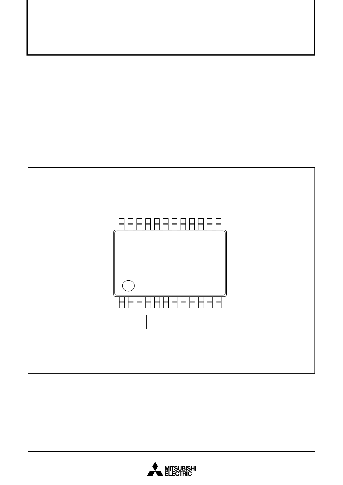
PIN CONFIGURATION (TOP VIEW)
0
EE
DIG
V
→
←
2
1
DIG
←
←
DIG
3
DIG
←
FEATURES
●Digit output.............................................................16 (maximum)
•Up to 16 pins can be selected
•More digits available by connecting additional M35501FPs
•Output structure: high-breakdown voltage, P-channel opendrain; built-in pull-down resistor between digit output pins and
VEE pin
●Power-on reset circuit........................................................ Built-in
●Power source voltage ................................................ 4.0 to 5.5 V
●Pull-down power source voltage ................................ Vcc – 43 V
●Operating temperature range...................................–20 to 85 °C
●Package ............................................................................. 24P2E
●Power dissipation ...............250µW (at 100 kHz operation clock)
6
←
4
DIG
←
5
DIG
←
DIG
←
7
DIG
8
9
10
DIG
DIG
←
15161718192021222324
DIG
←
←
14
13
Fig. 1 Pin configuration of M35501FP
M35501FP
123456789101112
→
13
DIG
12
DIG
→
11
DIG
→
SS
V
←
CLK
CC
V
←
RESET
←
SEL
←
IN
OVF
→
OUT
OVF
15
DIG
Outline: 24P2E-A
24-pin plastic-molded SSOP
→
→
14
DIG
FUNCTIONAL BLOCK
OVFOUT
7
6
OVFIN
3
CC
V
VSS
1
4
RESET
DIG15 DIG14 DIG13 DIG12 DIG11 DIG10 DIG9 DIG8 DIG7 DIG6 DIG5 DIG4 DIG3 DIG2 DIG1 DIG0
16
8
10
9
11
14
13
12
15
17
20
1918
21
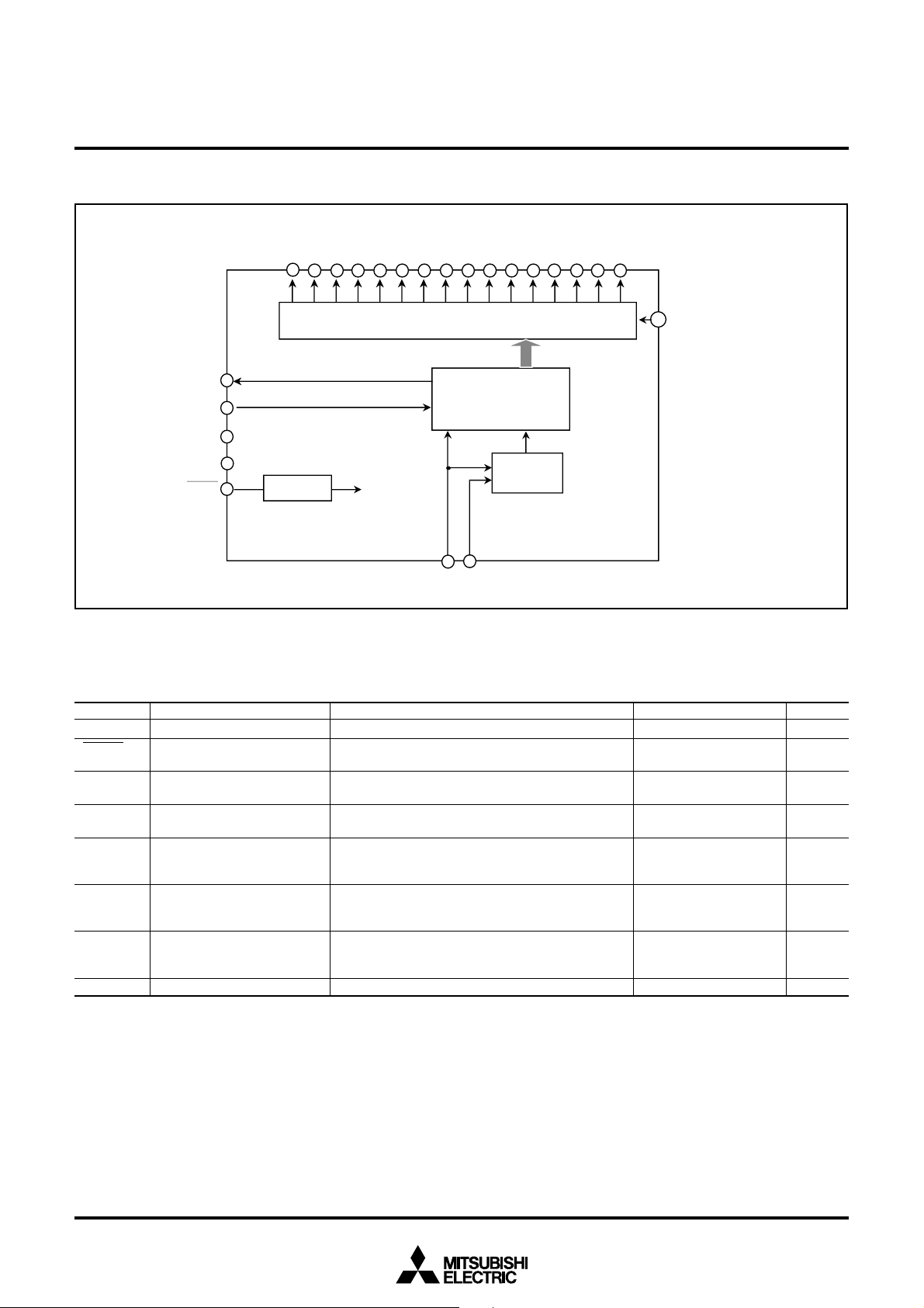
Shift register
Optional digit
Power-on
reset
counter
MITSUBISHI IC’S
M35501FP
FLD (VFD) DIGIT EXPANDER
2322
VEE
24
Fig. 2 Functional block diagram
PIN DESCRIPTION
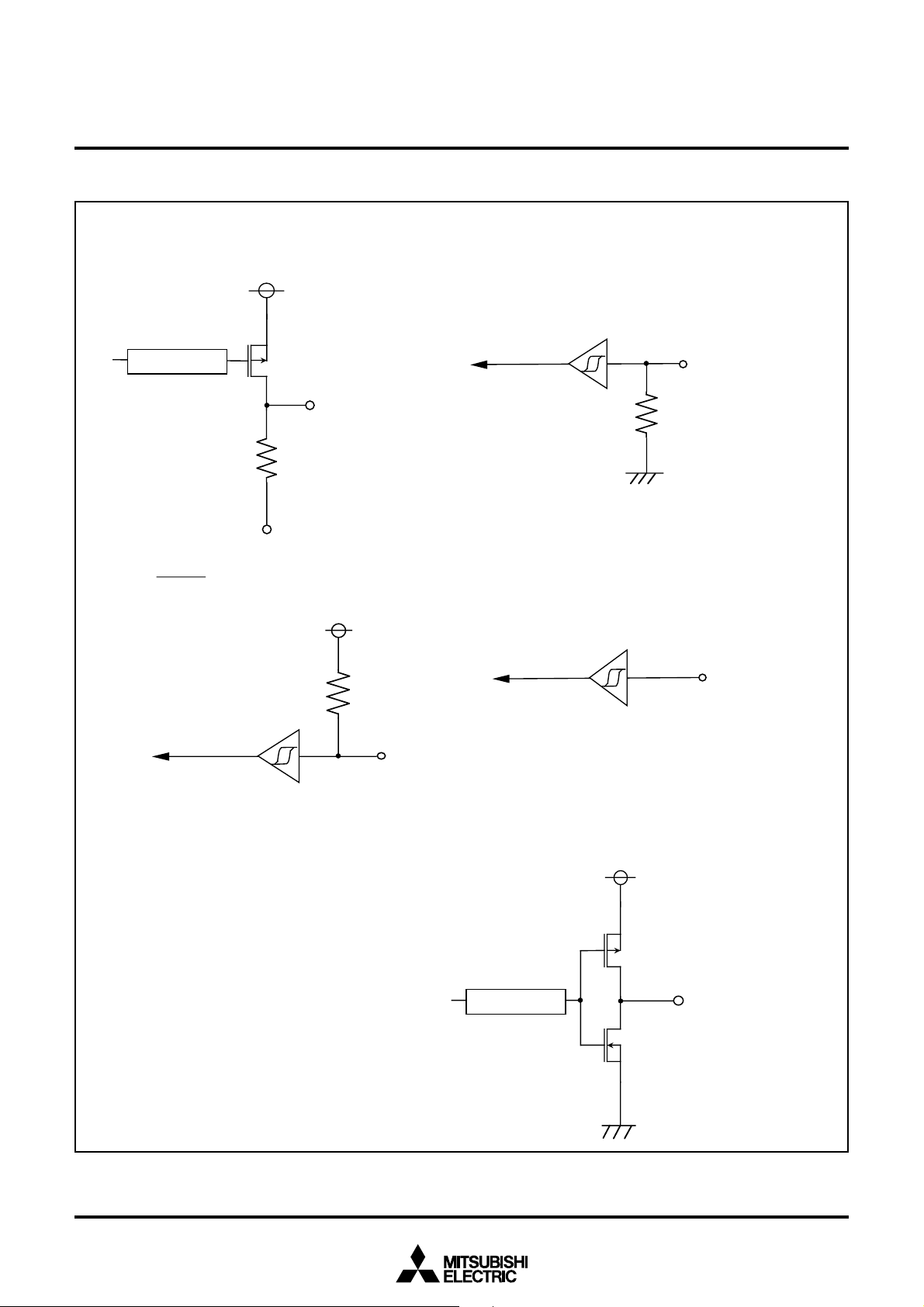
Table 1 Pin description
Pin
VCC, VSS
RESET
CLK
SEL
OVFIN
OVFOUT
DIG15–
DIG0
VEE
Power source input
Reset input
Clock input
Select input
Overflow signal input
Overflow signal output
Digit output
Pull-down power source input
Name
5
2
CLK SEL
Function
Apply 4.0–5.5 V to Vcc, and 0V to Vss.
Reset internal shift register (built-in power-on reset
circuit).
Digit output varies according to rising edge of clock
input.
Use when specifying the number of digits.
Input “H” when using one M35501FP. Connect to
OVFOUT pin of additional M35501FPs when using
multiple M35501FPs (to use 17 digits or more).
Leave open when using one M35501FP. Connect to
OVFIN pin of additional M35501FPs when using multiple
M35501FPs (to use 17 digits or more).
Output the digit output waveform of fluorescent
display. Leave open when not in use (VEE level
output).
Apply voltage to DIG0–DIG15 pull-down resistors.
Output Structure
–
CMOS input level
Built-in pull-up resistor
CMOS input level
Built-in pull-down resistor
CMOS input level
Built-in pull-down resistor
CMOS input level
CMOS output
High-breakdown-voltage
P-channel open-drain output
Built-in pull-down resistor
–
Fig. No.
–
3
2
2
4
5
1
–
2
PORT BLOCK
MITSUBISHI IC’S
M35501FP
FLD (VFD) DIGIT EXPANDER
(1) DIG0–DIG15
Shift register
(3) RESET
(2) SEL, CLK
Pull-down transistor
V
EE
(4) OVF
Pull-up transistor
IN
Fig. 3 Port block diagram
(5) OVFOUT
Shift register
3
USAGE
Three usages of the M35501FP are described below.
(1) 16-Digit Mode: 16 digits selected
The number of digits is set to 16 by fixing the OVFIN pin to “H” and
the SEL pin to “L.” Figure 5 shows the output waveform.
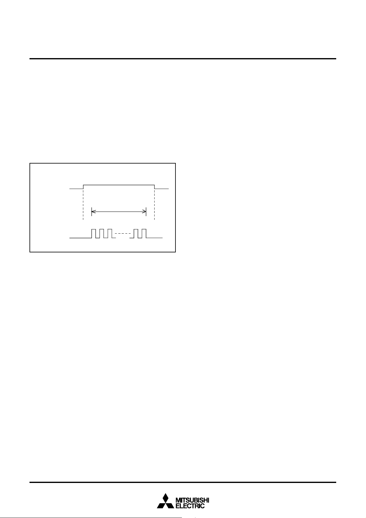
(2) Optional Digit Mode: 1-16 digits selectable
When the number of CLK pin rising edges during an “H” period of
the SEL pin is n and the OVFIN pin is fixed to “H,” the number of
digits set is n. If n is 16 or more, all 16 digits are set. Figure 6
shows the output waveform.
SEL pin
MITSUBISHI IC’S
M35501FP
FLD (VFD) DIGIT EXPANDER
n
CLK pin
Fig. 4 Digit setting
(3) Cascade Mode: 17 digits or more selectable
17 digits or more can be used by connecting two M35501FPs or
more. Figure 7 shows an example using three M35501FPs, offering
33 to 48 digit outputs.
Cascade mode will not operate if all M35501FPs are in 16-digit
mode (SEL = “L”). Use the most significant M35501FP in the optional
digit mode for DIG output. Figure 8 shows the output waveform.
4
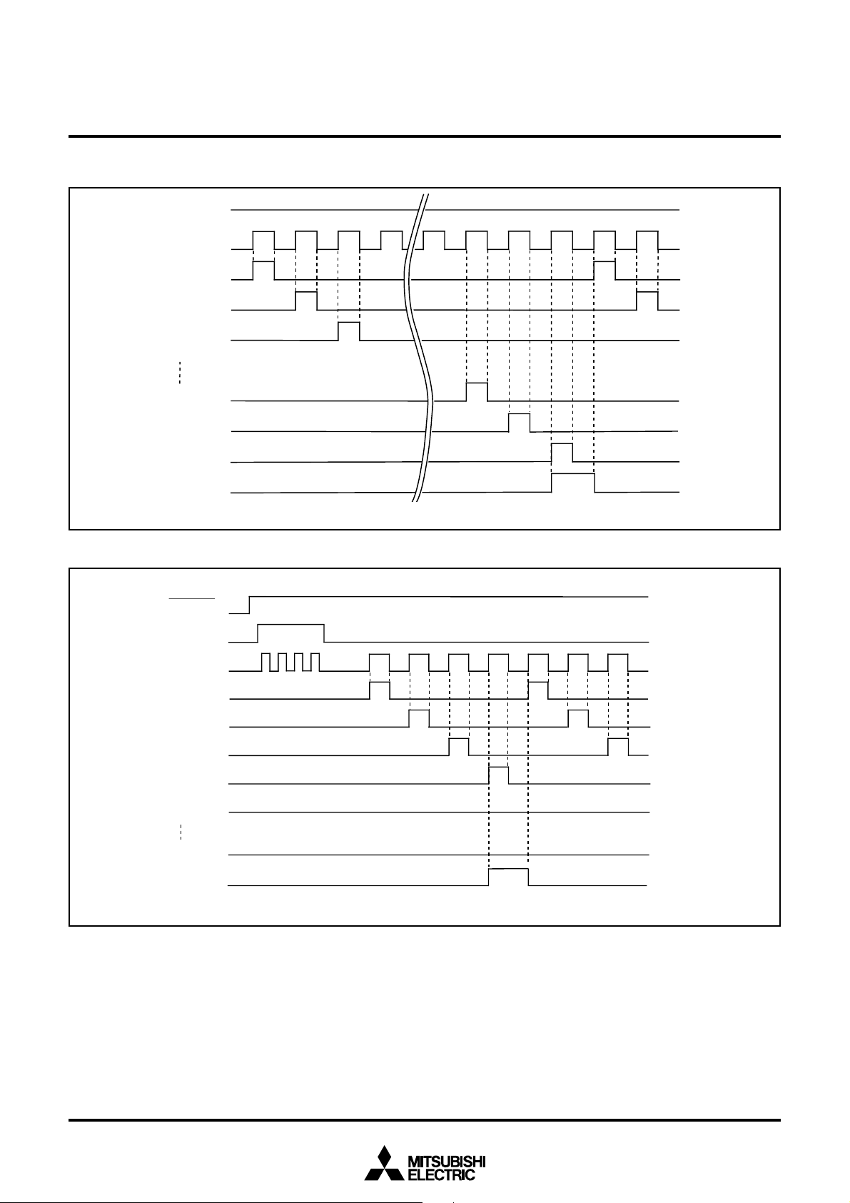
DIGIT OUTPUT WAVEFORM
MITSUBISHI IC’S
M35501FP
FLD (VFD) DIGIT EXPANDER
SEL
“L”
CLK
DIG
0
DIG1
DIG2
DIG13
DIG14
DIG15
OVFOUT
Fig. 5 16-digit mode output waveform
RESET
SEL
CLK
DIG
0
DIG
1
DIG
2
DIG
3
4
15
OUT
“L”
“L”
DIG
DIG
OVF
Fig. 6 Optional digit mode output waveform
5

RESET
CLK
Select signal
RESET
CLK
SEL
RESET
CLK
SEL
OVF
OVF
OVF
OVF
MITSUBISHI IC’S
M35501FP
FLD (VFD) DIGIT EXPANDER
IN(1)
DIG0
DIG1
DIG14
DIG15
OUT(1)
IN(2)
DIG16
DIG17
DIG30
DIG31
OUT(2)
IN(3)
OVF
RESET
CLK
SEL
OUT(3)
OVF
Fig. 7 Cascade mode connection example: 17 digits or more selected
CLK
RESET
DIG
0
DIG
1
DIG
2
DIG
15
DIG32
DIG33
DIG46
DIG47
OVF
OUT
(1)
DIG
16
DIG
17
DIG
31
OVF
OUT
(2)
Fig. 8 Cascade mode output waveform
6

The number of fluorescent displays can be increased by connecting
Fluorescent Display (FLD)
Fluorescent Display (FLD)
the M35501FP to the CMOS FLD output pins on a 38B5 Group microcomputer.
MITSUBISHI IC’S
M35501FP
FLD (VFD) DIGIT EXPANDER
Segment (high-breakdown-voltage: 36 pins + CMOS: 4 pins)
(1 pin used as CLK.)
P27–P2
0
P07–P0
M38B5X
P8
4
P17–P1
P37–P3
P83–P8
SEL
M35501
0
0
0
0
Digits
0
–DIG
DIG
15
CLK
Fig. 9 Connection example with 38B5 Group microcomputer (1 to 16 digits)
This FLD controller can control up to 32 digits using the 32 timing
mode of the 38B5 Group microcomputer.
Segment (high-breakdown-voltage: 36 pins + CMOS: 4 pins)
P27–P2
0
P07–P0
M38B5X
4
P8
P17–P1
P37–P3
P83–P8
0
0
0
0
(1 pin is used as CLK.)
SEL
M35501
CLK
OVF
OVF
SEL
OUT
IN
OVF
OVF
OUT
Digits
0
–DIG
16
–DIG
15
31
DIG
IN
Digits
DIG
M35501
CLK
Fig. 10 Connection example with 38B5 Group microcomputer (17 to 32 digits)
7

MITSUBISHI IC’S
M35501FP
FLD (VFD) DIGIT EXPANDER
RESET CIRCUIT
To reset the controller, the RESET pin should be held at “L” for 2
µs or more. Reset is released when the RESET pin is returned to
“H” and the power source voltage is between 4.0 V and 5.5 V.
RESET
CLK
0
DIG
DIG
1
DIG
2
DIG
3
Notes1: Perform the reset release when CLK input signal is “L.”
2: When setting the number of digits by SEL signal, optional digit
counter is set to “0” by reset.
Fig. 11 Digit output waveform when reset signal is input
8

MITSUBISHI IC’S
M35501FP
FLD (VFD) DIGIT EXPANDER
POWER-ON RESET
Reset can be performed automatically during power on (power-on
reset) by the built-in power-on reset circuit. When using this circuit, set 100 µs or less for the period in which it takes to reach
minimum operation guaranteed voltage from reset.
Pull-up transistor
RESET
pin
(Note)
Note:
Applied voltage to the RESET pin must be VDD or less.
Power-on reset
circuit
This symbol represents a parasitic diode.
If the rising time exceeds 100 µs, connect the capacitor between
the RESET pin and VSS at the shortest distance. Consequently,
the RESET pin should be held at “L” until the minimum operation
guaranteed voltage is reached.
VDD
Power-on reset circuit
output voltage
Reset state
Internal reset signal
Power-on
Reset released
Fig. 12 Power-on reset circuit
9

FLD (VFD) DIGIT EXPANDER
ABSOLUTE MAXIMUM RATINGS
ParameterSymbol Unit
VCC
VEE
VI
VI
VO
VO
Pd
Topr
Tstg
RECOMMENDED OPERATING CONDITIONS (VCC = 4.0 to 5.5 V, Ta = –20 to 85 °C, unless otherwise noted)
VCC
VSS
VEE
VIH
VIH
VIL
VIL
Power source voltage
Pull-down power source voltage
Input voltage CLK, SEL, OVFIN
Input voltage RESET
Output voltage DIG0–DIG15
Output voltage OVFOUT
Power dissipation
Operating temperature
Storage temperature
Power source voltage
Power source voltage
Pull-down power source voltage
“H” input voltage CLK, SEL, OVFIN
“H” input voltage RESET
“L” input voltage CLK, SEL, OVF
“L” input voltage RESET
•All voltages are based on VSS.
•Output transistors are off.
Ta = 25 °C
ParameterSymbol Unit
IN
Conditions
–0.3 to 7.0
VCC –45 to VCC +0.3
–0.3 to VCC +0.3
–0.3 to VCC +0.3
VCC –45 to VCC +0.3
–0.3 to VCC +0.3
–40 to 125
Min.
4.0
VCC –43
0.8VCC
0.8VCC
0
0
MITSUBISHI IC’S
M35501FP
Ratings
250
–20 to 85
Limits
Typ.
5.0
0
Max.
5.5
VSS
VCC
VCC
0.2VCC
0.2VCC
V
V
V
V
V
V
mW
°C
°C
V
V
V
V
V
V
V
RECOMMENDED OPERATING CONDITIONS (VCC = 4.0 to 5.5 V, Ta = –20 to 85 °C, unless otherwise noted)
ParameterSymbol Unit
IOH(peak)
IOH(peak)
IOL(peak)
IOH(avg)
IOH(avg)
IOL(avg)
CLK
Notes 1: The peak output current is the peak current flowing in each port.
2: The average output current is an average value measured over 100 ms.
“H” peak output current DIG0 – DIG15 (Note 1)
“H” peak output current OVFOUT (Note 1)
“L” peak output current OVFOUT (Note 1)
“H” average current DIG0 – DIG15 (Note 2)
“H” average current OVFOUT (Note 2)
“L” average current OVFOUT (Note 2)
Clock input frequency
Min.
Limits
Typ.
Max.
–36
–10
10
–18
–5.0
5.0
2
mA
mA
mA
mA
mA
mA
MHz
10

ELECTRICAL CHARACTERISTICS (VCC = 4.0 to 5.5 V, Ta = –20 to 85 °C, unless otherwise noted)
Test conditionsParameterSymbol
VOH
VOH
VOL
VT+—VT–
IIH
IIH
IIL
IIL
ILOAD
ILEAK
ICC
“H” output voltage
“H” output voltage
“L” output voltage
Hysteresis
“H” input current
“H” input current
“L” input current
“L” input current
Output load current
Output leakage current
Power source
DIG output
DIG0–DIG15
OVFOUT
OVFOUT
CLK, OVFIN
RESET
OVFIN
RESET
CLK, SEL
OVFIN
CLK, SEL
RESET
DIG0 – DIG15
DIG0–DIG15
VCC = 5.0 V, CLK = 100 kHz
Output transistors are off.
IOH = –18 mA
IOH = –10 mA
IOL = 10 mA
VCC = 5.0 V
VI = VCC
VI = VCC
VCC = 5.0 V
VI = VSS
VI = VSS
VCC = 5.0 V
VEE = VCC –43 V
VOL = VCC
Output transistors are off.
VEE = VCC –43 V
VOL = VCC –43 V
Output transistors are off.
VCC –2.0
VCC –2.0
MITSUBISHI IC’S
M35501FP
FLD (VFD) DIGIT EXPANDER
Limits
Min.
30
–60
500
Typ.
0.4
70
–130
650
50
Max.
2.0
5.0
140
–5.0
–185
800
–10
Unit
V
V
V
V
µA
µA
µA
µA
µA
µA
µA
11

TIMING REQUIREMENTS (VCC = 4.0 to 5.5 V, Ta = –20 to 85 °C, unless otherwise noted)
ParameterSymbol Unit
tw(RESET)
tc(CLK)
twH(CLK)
twL(CLK)
tsu(SEL)
th(SEL)
th(CLK)
Reset input “L” pulse width
Clock input cycle time
Clock input “H” pulse width
Clock input “L” pulse width
Select input setup time
Select input hold time
Clock input setup time
MITSUBISHI IC’S
M35501FP
FLD (VFD) DIGIT EXPANDER
Limits
Min.
2
500
200
200
500
500
500
Typ. Max.
µ
ns
ns
ns
ns
ns
ns
s
RESET
CLK
SEL
CLK
Fig. 13 Timing diagram
t
t
wL(CLK)
w(RESET)
t
c(CLK)
t
h(SEL)
0.8V
CC
t
h(CLK)
0.8V
t
wH(CLK)
CC
v
cc
v
ss
v
cc
v
ss
v
cc
v
ss
v
cc
v
ss
t
su(SEL)
0.2V
CC
0.2V
CC
12

Keep safety first in your circuit designs!
• Mitsubishi Electric Corporation puts the maximum effort into making semiconductor products better and more reliable, but there is always the possibility that trouble may occur with them. Trouble with
semiconductors may lead to personal injury, fire or property damage. Remember to give due consideration to safety when making your circuit designs, with appropriate measures such as (i) placement of
substitutive, auxiliary circuits, (ii) use of non-flammable material or (iii) prevention against any malfunction or mishap.
Notes regarding these materials
• These materials are intended as a reference to assist our customers in the selection of the Mitsubishi semiconductor product best suited to the customer’s application; they do not convey any license under any
intellectual property rights, or any other rights, belonging to Mitsubishi Electric Corporation or a third party.
• Mitsubishi Electric Corporation assumes no responsibility for any damage, or infringement of any third-party’s rights, originating in the use of any product data, diagrams, charts or circuit application examples
contained in these materials.
• All information contained in these materials, including product data, diagrams and charts, represent information on products at the time of publication of these materials, and are subject to change by Mitsubishi
Electric Corporation without notice due to product improvements or other reasons. It is therefore recommended that customers contact Mitsubishi Electric Corporation or an authorized Mitsubishi Semiconductor
product distributor for the latest product information before purchasing a product listed herein.
• Mitsubishi Electric Corporation semiconductors are not designed or manufactured for use in a device or system that is used under circumstances in which human life is potentially at stake. Please contact
Mitsubishi Electric Corporation or an authorized Mitsubishi Semiconductor product distributor when considering the use of a product contained herein for any specific purposes, such as apparatus or systems for
transportation, vehicular, medical, aerospace, nuclear, or undersea repeater use.
• The prior written approval of Mitsubishi Electric Corporation is necessary to reprint or reproduce in whole or in part these materials.
• If these products or technologies are subject to the Japanese export control restrictions, they must be exported under a license from the Japanese government and cannot be imported into a country other than the
approved destination.
Any diversion or reexport contrary to the export control laws and regulations of Japan and/or the country of destination is prohibited.
• Please contact Mitsubishi Electric Corporation or an authorized Mitsubishi Semiconductor product distributor for further details on these materials or the products contained therein.
© 1998 MITSUBISHI ELECTRIC CORP.
New publication, effective Feb. 1998.
Specifications subject to change without notice.

REVISION DESCRIPTION LIST M35501FP DATA SHEET
Rev. Rev.
No. date
1.0 First Edition 980216
Revision Description
(1/1)
 Loading...