

Page 1
MITSUBISHI <DIGITAL ASSP>
M35500AFP/BGP
FLD(VFD) CONTROLLER
DESCRIPTION/FEATURES
High-breakdown-voltage output port ......................................... 26
•
A-D converter ................................................... 8-bit ✕ 6 channels
•
• Segment output............................................ 8 to 18
• Digit output................................................... 7 to 10
(Ports P0 to P7 are also used as ordinary output ports)
• Output breakdown.................................. Vcc – 45 V
• Output current.................. –18 mA (DIG0 to DIG17),
–7 mA (SEG0 to SEG7)
• Pull-down resistor ........................................build-in
• Dimmer switch ............................................ 4 levels
• Absolute accuracy....................................... ±3 LSB
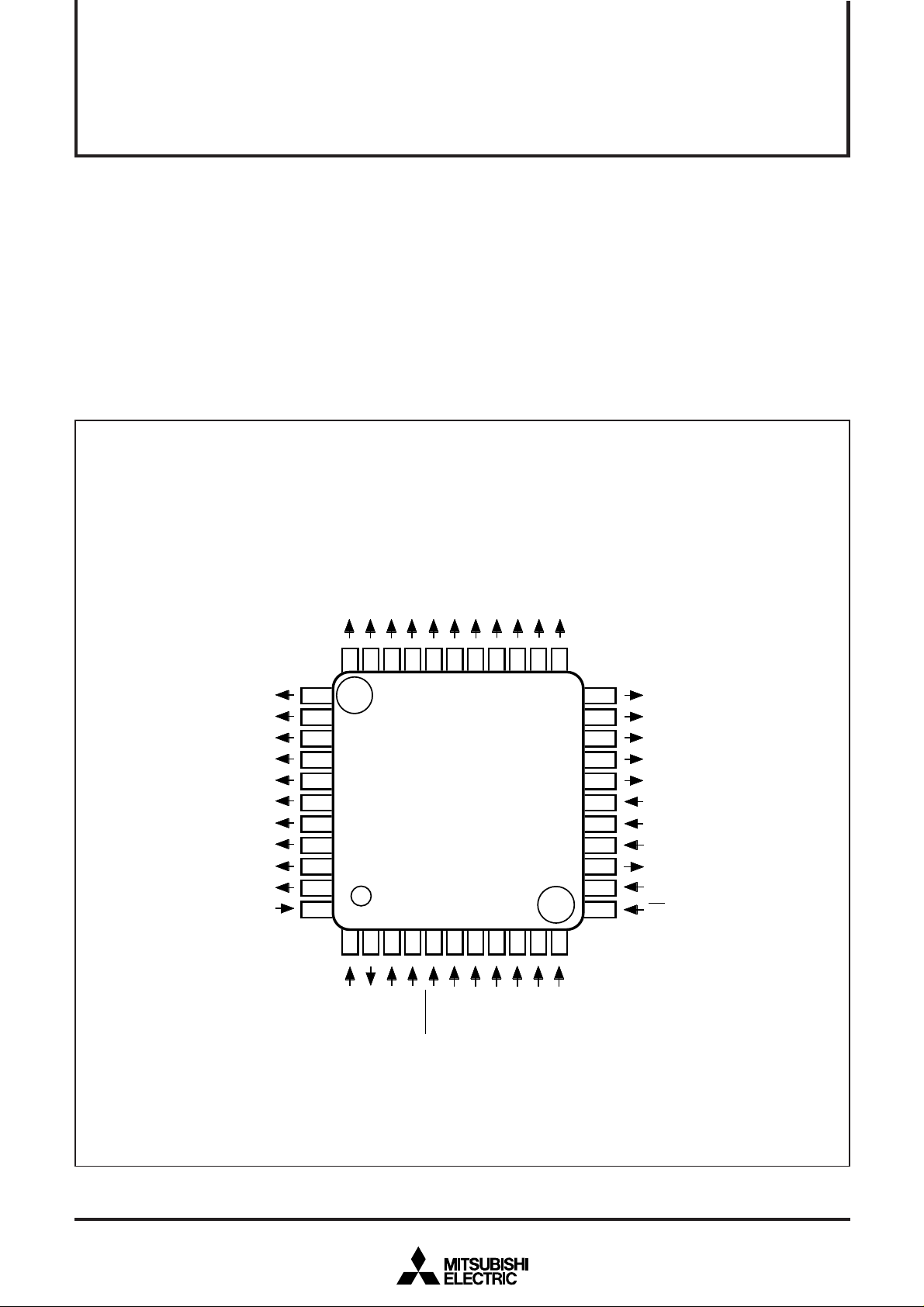
PIN CONFIGURATION (TOP VIEW)
0
1
2
1
1
1
G
G
G
/
/
/
5
4
3
1
1
1
G
G
G
D
I
D
I
S E
D
I
I
S E
S E
S E
Serial I/O ..................................... 4 (CS controller, external clock)
•
Package ................................................................. 44P6N/44P6X
•
Oscillating circuit ........... RC oscillating cirucit (external capacitor)
•
Power source voltage..................................................4.0 to 5.5 V
•
3
4
5
1
1
1
6
7
1
G
G
/
/
2
1
1
1
G
G
D
D
I
I
S E
S E
1
G
G
G
/
0
/
/
1
9
8
G
G
G
D
D
I
D
I
S E
S E
I
P
• Noise filter ....................................................build-in
(in serial input pin and clock pin, 2 MHz sampling)
• FLD display data ............................................. input
• A-D conversion data ..................................... output
• Command ....................................................... input
• Oscillating frequency.....................................4 MHz
7
5
/
/
/
6
7
5
G
G
G
P 6D
D
I
P
D
I
D I G
D I G
1 6
1 7
/ S E G
/ S E G
S E G
S E G
S E G
S E G
S E G
S E G
S E G
S E G
V
D D
2
1
3
33
9
3 4
8
3 5
7
3 6
6
3 7
5
3 8
4
3 9
3
4 0
2
4 1
1
4 2
0
4 3
9
3
03
2
82
M 3 5 5 0 0 A F P
M 3 5 5 0 0 B G P
4 4
1
2
3
4
5
S
T
D
D
V
U
N
T
I
S
X
O
V
X
R
6
7
2
2
52
6
7
8
5
4
3
N
N
N
A
A
A
2
42
9
2
N
A
3
2 2
2 1
2 0
1 9
1 8
1 7
1 6
1 5
1 4
1 3
1 2
0
1
1
1
1
0
N
N
A
A
D I G4/ P 4
D I G
3
/ P 3
D I G
2
/ P 2
D I G
1
/ P 1
D I G
0
/ P 0
E E
V
V
E E
S
C L K
S
O U T
S
I N
C S
E S E
Fig. 1. Pin configuration of M35500AFP/BGP
Package type: 44P6N-A/44P6X
1
Page 2
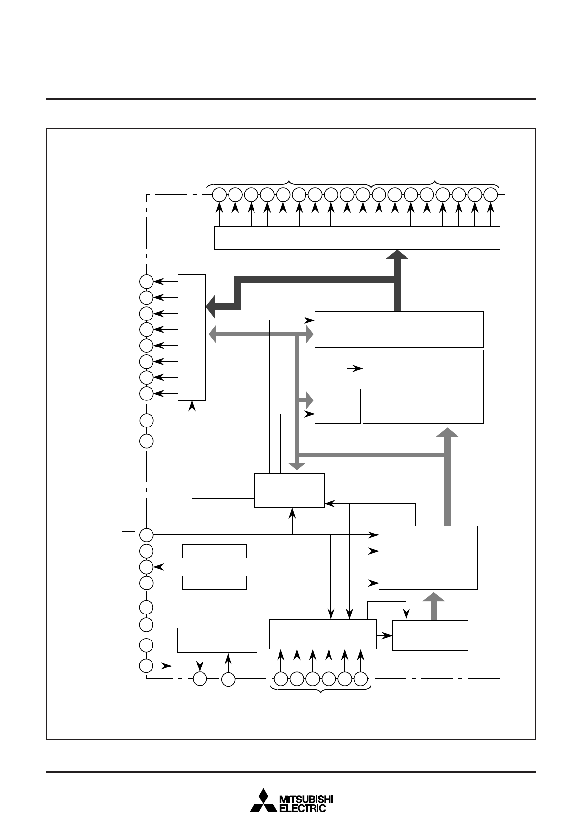
FUNCTIONAL BLOCK
MITSUBISHI <DIGITAL ASSP>
M35500AFP/BGP
FLD(VFD) CONTROLLER
DIG7/P7
6
/P6
DIG
5
/P5
DIG
DIG
4
/P4
3
/P3
DIG
DIG
2
/P2
1
/P1
DIG
0
/P0
DIG
V
EE
V
EE
25
24
23
22
21
20
19
18
17
16
DIG8/SEG17 – DIG17/SEG
Mode
register
Memory
address
Transfer
counter
8
SEG7 – SEG
0
434241403938373635343332313029282726
Display control circuit
Display RAM
Command
analytic circuit
12
CS
IN
S
S
OUT
S
CLK
V
DD
V
DD
V
SS
RESET
13
14
15
44
1
3
5
Noise filter
Noise filter
Clock generating
circuit
2
4
OUT
X
IN
X
Selector/A-D
control circuit
6 7 8 9 10 11
FUNCTIONAL BLOCK DIAGRAM (Package: 44P6N-A)
Fig. 2. Functional block diagram
AN5 – AN
Byte end
Serial I/O
Trigger
A-D
0
2
Page 3
PIN DESCRIPTION
Table. 1. Pin description
Pin
VCC, VSS
VEE
XIN
XOUT
______
RESET
____
CS
SCLK
SOUT
SIN
DIG0/P0 –
DIG7/P7
DIG8/SEG17 –
DIG17/SEG8
SEG0 – SEG7
Name
Power source
Pull-down
power source
Clock input
Clock output
______
RESET input
Chip select
Serial clock
Serial output
Serial input
Digit/Port
Digit/Segment
Segment
Input
Input
CMOS input
CMOS input
CMOS input
Noise filter
CMOS input
Noise filter
Output
Output
N-channel
open-drain
P-channel
open-drain
P-channel
open-drain
P-channel
open-drain
MITSUBISHI <DIGITAL ASSP>
M35500AFP/BGP
FLD(VFD) CONTROLLER
Function
• Apply voltage of 5 V to VCC, and 0 V to VSS.
• Applies voltage supplied to pull-down resistors.
• RC oscillator pins for system clock.
• Reset input pin for active “L”.
• Internal pull-up resistors connected between the RESET and VCC pins.
• Serial transfer is possible by inputting “L” signal.
• Clock for serial transfer is input.
•
Read a clock twice with 2 MHz sampling clock and judge if it is a noise or not.
• Serial data is output.
• During reset it is in high-impedance state.
• Serial data is input.
•
Read a clock twice with 2 MHz sampling clock and judge if it is a noise or not.
• Pin for ordinary output or digit output.
• At reset this port is set to VEE level through a pull-down resistor.
• Pin for digit output or segment output.
• At reset this port is set to VEE level through a pull-down resistor.
• Pin for segment output.
• At reset this port is set to VEE level through a pull-down resistor.
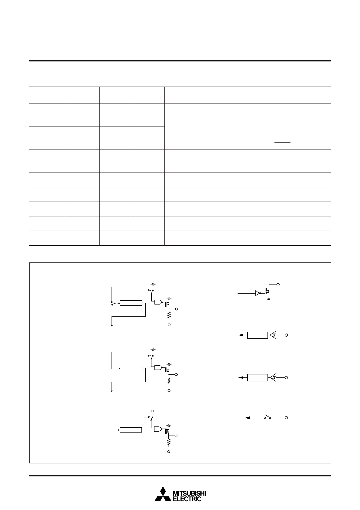
PORT BLOCK
(1) Digit/Port pin
Digit/Segment pin
Shift signal from high-order
Data bus
Segment data
Shift signal to low-order
(2) Digit pin
Shift signal from high-order
Shift signal to low-order
(3) Segment pin
Segment data
Dimmer signal
(Note)
latch
Dimmer signal
(Note)
latch
Dimmer signal
(Note)
latch
(4) S
OUT
pin
S
OUT
signal
✽
V
EE
✽
V
EE
✽
(5) CS pin
CS input
IN
, S
CLK
(6) S
(7) A-D input
pin
Serial input
Serial clock input
A-D conversion input
Noise filter
Noise filter
Fig. 3. Port block diagram
✽ High-breakdown-voltage P-channel transistor
V
EE
Note: Dimmer signal is for setting the Toff time.
3
Page 4
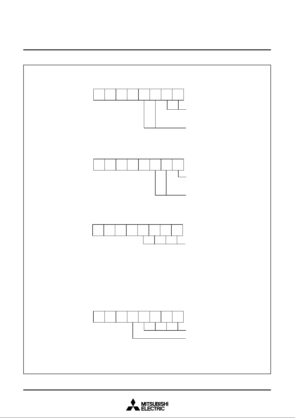
COMMAND STYLE
Display data setting
(Command 0)
111
MITSUBISHI <DIGITAL ASSP>
M35500AFP/BGP
FLD(VFD) CONTROLLER
b0b1b2b3b4b5b6b7
—
Number of segment setting
0 0 : 16 or less
0 1 : 17 or more
Number of digit setting
0 0 : 7
0 1 : 8
1 0 : 9
1 1 : 10
Display state setting
(Command 1)
Digit selection
(Command 2)
Port data setting
(Command 3)
110
10
100
1
——
—
Display ON or OFF setting
1 : ON
0 : OFF
Display duty setting
1 1 : 15/16
1 0 : 14/16
0 1 : 6/16
0 0 : 5/16
Digit start pin setting
0 0 0 0 : D
0 0 0 1 : D16
0 0 1 0 : D15
0 0 1 1 : D14
0 1 0 0 : D13
0 1 0 1 : D12
0 1 1 0 : D11
0 1 1 1 : D10
1 0 0 0 : D9
1 0 0 1 : D8
1 0 1 0 : D7
17
Note: When a digit or a port has to be selected, a digit output is selected for having higher priority.
Fig. 4. Command style
4
P3 – P0/P7 – P4 output data
Port selection (Note)
0 : P3 – P0
1 : P7 – P4
Page 5
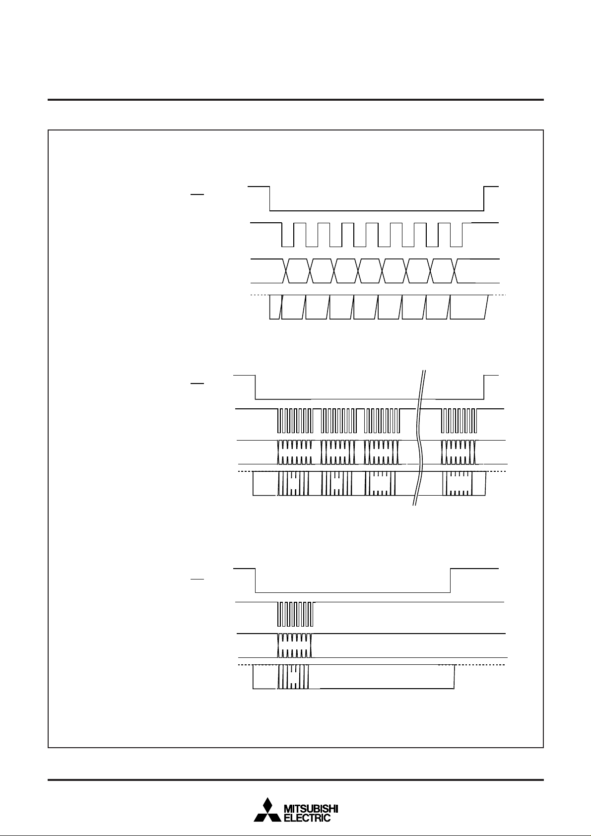
0
SERIAL I/O PROTOCOL
Byte protocol
MITSUBISHI <DIGITAL ASSP>
M35500AFP/BGP
FLD(VFD) CONTROLLER
CS
CLK
Command protocol
Display data setting
(Command 0)
S
IN
S
OUT
CS
CLK
S
IN
S
OUT
b0 b1 b2 b3 b4 b5 b6 b7
X
b0 b1 b2 b3 b4 b5 b6 b7
OUT
Note: S
Note 1: The serial data which is transmitted after executing command
Note 2: Set the CS signal to “H” level after transferring a display data.
is in high-impedance state during CS signal is “H”.
Command 0 Data 1 Data 2
X
is recognized as a display data.
“A-D data 6 or more” data is defined as an undefined “X”.
X
A-D
data 0
Data i
A-D
data j
Other setting except
display data setting
(Command 1 to 3)
Fig. 5. Serial I/O protocol
CS
CLK
S
IN
S
OUT
Command
X
5
Page 6

SERIAL COMMUNICATION FORMAT (DISPLAY DATA, A-D OUTPUT)
17 or more segments (3-byte transfer)
CS
CLK
MITSUBISHI <DIGITAL ASSP>
M35500AFP/BGP
FLD(VFD) CONTROLLER
S
S
IN
OUT
Command 0
SEG
0-7
X XX XXX
Note: 2 bytes “X” data is output before outputting AD valid data.
16 or less segments (2-byte transfer)
CS
CLK
S
S
IN
OUT
Command 0
8 or less segments (2-byte transfer)
SEG
0-7
XX XX XXX
Note: 2 bytes “X” data is output before outputting AD valid data.
SEG
8-15
AD0AD1AD2AD3AD4AD
X
SEG
8-15
DIG n
AD0AD1AD2AD3AD4AD
SEG
SEG
16-17
SEG
0-7
DIG n-1 DIG n-3
SEG
0-7
8-15
DIG n-1 DIG n-2 DIG 0DIG n
AD valid data
SEG
SEG
8-15
0-7
AD valid data
SEG
16-17
SEG
8-15
DIG n-2
SEG
0-7
5
SEG
0-7
5
SEG
8-15
SEG
8-15
SEG
16-17
SEG
0-7
SEG
0-7
SEG
8-15
SEG
0-7
DIG 0
SEG
16-17
SEG
8-15
CS
CLK
S
IN
S
OUT
Fig. 6. Serial communication format
6
Command 0
SEG
0-7
XX XX XXX
SEG
dummy
0-7
data
DIG n-1 DIG n-3
AD0AD1AD2AD3AD4AD
SEG
dummy
0-7
data
AD valid data
DIG n-2 DIG 0DIG n
dummy
data
SEG
0-7
5
dummy
data
SEG
0-7
SEG
0-7
dummy
data
Note: 2 bytes “X” data is output before outputting AD valid data.
Page 7

FLD DISPLAY TIMING
G n
G n-1
G 1
Segment
output
MITSUBISHI <DIGITAL ASSP>
M35500AFP/BGP
FLD(VFD) CONTROLLER
Tdisp
Digit
Segment
Toff
Fig. 7. FLD display timing diagram
SEGMENT/DIGIT SETTING EXAMPLE
10
11
12
13
14
15
16
17
18
19
20
21
22
23
24
25
26
PORT
1
2
3
4
5
6
7
8
9
P7
P6
P5
P4
P3
P2
P1
P0
DIG
DIG17
DIG16
DIG15
DIG14
DIG13
DIG12
DIG11
DIG10
DIG9
DIG8
DIG7
DIG6
DIG5
DIG4
DIG3
DIG2
DIG1
DIG0
Tdisp
SEG
SEG0
SEG1
SEG2
SEG3
SEG4
SEG5
SEG6
SEG7
SEG8
SEG9
SEG10
SEG11
SEG12
SEG13
SEG14
SEG15
SEG16
SEG17
Grid : 7
Segment : 8
S1
S2
S3
S4
S5
S6
S7
S8
G7
G6
G5
G4
G3
G2
G1
Tscan = 0ns
Tdisp = 384 µs
(oscillation frequency f(X
Toff= 264 µs ( 5/16 ✕ Tdisp)
240 µs ( 6/16 ✕ Tdisp)
48 µs (14/16 ✕ Tdisp)
24 µs (15/16 ✕ Tdisp)
Grid : 10
Segment: 8
S1
S2
S3
S4
S5
S6
S7
S8
G10
G9
G8
G7
G6
G5
G4
G3
G2
G1
Grid : 10
Segment: 16
S1
S2
S3
S4
S5
S6
S7
S8
S9
S10
S11
S12
S13
S14
S15
S16
G10
G9
G8
G7
G6
G5
G4
G3
G2
G1
Grid : 7
Segment: 18
S1
S2
S3
S4
S5
S6
S7
S8
S9
S10
S11
S12
S13
S14
S15
S16
S17
S18
G7
G6
G5
G4
G3
G2
G1
IN
) = 4.0 MHz)
Fig. 8. Segment/Digit setting example
7
Page 8

BIT ALLOCATION FOR DISPLAY RAM
MITSUBISHI <DIGITAL ASSP>
M35500AFP/BGP
FLD(VFD) CONTROLLER
A D D R E S S
1 6
0 9
0 A1
0 B1
0 D1
0 E1
0 F1
1 11
1 21
1 31
1 51
1 61
1 71
1 91
1 A1
1 B1
1 D1
1 E1
1 F1
2 11
2 21
2 3
1 6
2 51
2 61
2 71
2 91
2 A1
2 B1
2 D1
2 E1
2 F1
b 7b
S E G
S E G
S E G
S E G
S E G
6
1 5
1 4
1 3
1 2
S E G7S E G6S E G5S E G4S E G3S E G2S E G1S E G
6
6
S E G
S E G
S E G
6
1 5
1 4
S E G7S E G6S E G5S E G4S E G3S E G2S E G1S E G
6
6
S E G
6
6
6
6
6
6
6
6
6
6
6
6
6
6
6
6
6
6
6
6
6
6
S E G
1 5
1 4
S E G7S E G6S E G5S E G4S E G3S E G2S E G1S E G
S E G
S E G
1 5
1 4
S E G7S E G6S E G5S E G4S E G3S E G2S E G1S E G
S E G
S E G
1 5
1 4
S E G7S E G6S E G5S E G4S E G3S E G
S E G
S E G
1 5
1 4
S E G7S E G6S E G5S E G4S E G3S E G2S E G1S E G
S E G
S E G
1 5
1 4
S E G7S E G6S E G5S E G4S E G3S E G2S E G1S E G
S E G
S E G
1 5
1 4
S E G7S E G6S E G5S E G4S E G3S E G2S E G1S E G
S E G
S E G
1 5
1 4
S E G7S E G6S E G5S E G4S E G3S E G2S E G1S E G
S E G
S E G
1 5
1 4
S E G7S E G6S E G5S E G4S E G3S E G2S E G1S E G
1 3
S E G
1 3
S E G
1 3
S E G
1 3
S E G
1 3
S E G
1 3
S E G
1 3
S E G
1 3
S E G
1 3
S E G
1 2
S E G
1 2
S E G
1 2
S E G
1 2
S E G
1 2
S E G
1 2
S E G
1 2
S E G
1 2
S E G
1 2
1 1
S E G
1 1
S E G
1 1
S E G
1 1
S E G
1 1
S E G
1 1
S E G
1 1
S E G
1 1
S E G
1 1
S E G
1 1
S E G
1 0
S E G
1 0
S E G
1 0
S E G
1 0
S E G
1 0
2
S E G
1 0
S E G
1 0
S E G
1 0
S E G
1 0
S E G
1 0
S E G
S E G
1 7
1 6
S E G9S E G
8
0
S E G
S E G
1 7
1 6
S E G9S E G
8
0
S E G
S E G
1 7
1 6
S E G9S E G
8
0
S E G
S E G
1 7
1 6
S E G9S E G
8
0
S E G
S E G
1 7
1 6
S E G9S E G
8
S E G1S E G
0
S E G
S E G
1 7
1 6
S E G9S E G
8
0
S E G
S E G
1 7
1 6
S E G9S E G
8
0
S E G
S E G
1 7
1 6
S E G9S E G
8
0
S E G
S E G
1 7
1 6
S E G9S E G
8
0
S E G
S E G
1 7
1 6
S E G9S E G
8
0
0
D i g i t 0
D i g i t 1
D i g i t 2
D i g i t 3
D i g i t 4
D i g i t 5
D i g i t 6
D i g i t 7
D i g i t 8
D i g i t 9
Fig. 9. Bit allocation for display RAM
8
Page 9

RESET CIRCUIT
To reset the controller, the RESET pin should be held at a “L” level
for 2 µs or more. Then the RESET pin is returned to an “H” level (the
power source voltage should be between 4.0 V and 5.5 V, and XIN
oscillation is stable), reset is released.
Make sure that the reset input voltage is 0.5 V or less for 4.0 V of
VCC.
V
R E S E T
C C
0 V
MITSUBISHI <DIGITAL ASSP>
M35500AFP/BGP
FLD(VFD) CONTROLLER
P o w e r o n
( N o t e )
0 V
Fig. 10. Reset circuit example
CLOCK GENERATING CIRCUIT
Oscillating circuit is built up by connecting pins XIN and XOUT as short
as possible and connecting a capacitor between pins XIN (XOUT) and
VSS.
When supplying a clock externally, input it to XIN pin and leave XOUT
pin open.
XI
N XO U T
S
CO
C
C C
0 . 2 V
N o t e . R e s e t r e l e a s e v o l t a g e :V
X
I N
E x t e r n a l o s c i l l a t i o n
c i r c u i t
V
C C
V
S S
C C
= 4 . 0 V
X
O U T
O p e n
Fig. 11. RC generating circuit Fig. 12. External clock input circuit
HANDLING OF UNUSED PINS
Handle unused pins as the follow.
Table. 2. Handling of unused pins
Pin
Segment
Digit
Analog input
Open
Open
Connect to VCC or VSS through a resistor.
Handling
9
Page 10

ABSOLUTE MAXIMUM RATINGS
MITSUBISHI <DIGITAL ASSP>
M35500AFP/BGP
FLD(VFD) CONTROLLER
VCC
VEE
VI
VI
VI
VO
VO
Pd
Topr
Tstg
Power source voltage
Pull-down power source voltage
Input voltage AN0 – AN5
Input voltage CS, SIN, SCLK
Input voltage RESET
Output voltage DIG0 – DIG17
SEG0 – SEG17
Output voltage SOUT
Power dissipation
Operating temperature
Storage temperature
RECOMMENDED OPERATING CONDITIONS
ParameterSymbol Unit
VCC
VSS
VEE
VIH
VIH
VIL
VIL
Power source voltage
Power source voltage
Pull-down power source voltage
“H” input voltage CS, SIN, SCLK
“H” input voltage RESET
“L” input voltage CS, SIN, SCLK
“L” input voltage RESET
ConditionsParameterSymbol Unit
•All voltage are based on VSS.
•Output transistors are cut off.
•All voltage are based on VSS.
•Output transistors are cut off.
•A waveform: 450 µs or more
frequency and 30 µs or less
pulse width.
•Connect only capacitor load
(CL = 200pF).
•All voltage are based on VSS.
•Output transistors are cut off.
Ta = 25 °C
(VCC = 4.0 to 5.5 V, Ta = –20 to 85 °C, unless otherwise noted)
Min.
4.0
VCC–38
0.75VCC
0.8VCC
0
0
Ratings
–0.3 to 7.0
VCC–45 to VCC+0.3
–0.3 to VCC+0.3
–0.3 to VCC+0.3
–0.3 to VCC+0.3
VCC–45 to VCC+0.3
VCC–50 to VCC+0.3
–0.3 to VCC+0.3
600
–20 to 85
–40 to 125
Limits
Typ.
5.0
0
Max.
VCC
VCC
VCC
0.25VCC
0.2VCC
5.5
V
V
V
V
V
V
V
mW
°C
°C
V
V
V
V
V
V
V
RECOMMENDED OPERATING CONDITIONS (VCC = 4.0 to 5.5 V, Ta = –20 to 85 °C, unless otherwise noted)
ParameterSymbol Unit
ΣIOH(peak)
ΣIOH(avg)
IOH(peak)
IOH(peak)
IOL(peak)
IOH(avg)
IOH(avg)
IOL(avg)
f(XIN)
f(SCLK)
Notes 1: The total output current is the sum of all the currents flowing through all the applicable ports. The total average current is an average
2: The peak output current is the peak current flowing in each port.
3: The average output current is an average value measured over 100 ms.
4: When the oscillation frequency has a 50 % duty cycle.
10
“H” total peak output current DIG0 – DIG17, SEG0 – SEG17 (Note 1)
“H” total peak output current DIG0 – DIG17, SEG0 – SEG17
“H” peak output current DIG0 – DIG17 (Note 2)
“H” peak output current SEG0 – SEG7 (Note 2)
“L” peak output current SOUT
“H” peak output current DIG0 – DIG17 (Note 3)
“H” peak output current SEG0 – SEG7 (Note 3)
“L” peak output current SOUT
Main clock input oscillation frequency (Note 4)
Serial I/O external clock frequency
value measured over 100 ms. The total peak current is the peak value of all the currents.
Min. Typ.
Limits
4.0
250
Max.
–240
–120
–40
–20
10
–18
–7
5.0
5.2
mA
mA
mA
mA
mA
mA
mA
mA
MHz
kHz
Page 11

MITSUBISHI <DIGITAL ASSP>
M35500AFP/BGP
FLD(VFD) CONTROLLER
ELECTRICAL CHARACTERISTICS (VCC = 4.0 to 5.5 V, Ta = –20 to 85 °C, unless otherwise noted)
Limits
Typ.
–150
–4.0
VOH
VOL
VT+—VT–
IIH
IIL
ILOAD
ILEAK
“H” output voltage
“L” output voltage
Hysteresis
“H” input voltage
“L” input voltage
Output load current
Output leakage
current
DIG output
SEG output
SOUT
SIN, SCLK, CS
RESET, XIN
SIN, SCLK, CS
RESET
XIN
SIN, SCLK, CS
RESET
XIN
DIG0 – DIG17
SEG0 – SEG17
DIG0 – DIG17
SEG0 – SEG17
Test conditionsParameterSymbol
IOH = –18 mA
IOH = –7 mA
IOL = 5 mA
VCC = 5.0 V
VI = VCC
VI = VSS
VEE = VCC–36 V
VOL = VCC
Output transistors “off”
VEE = VCC–38 V
VOL = VCC–38 V
Output transistors “off”
Min.
VCC–2.0
VCC–2.0
250
0.5
0.5
4.0
500
Max.
2.0
5.0
5.0
–5.0
750
–10
Unit
V
V
V
V
V
µA
µA
µA
µA
µA
µA
µA
µA
ELECTRICAL CHARACTERISTICS (VCC = 4.0 to 5.5 V, Ta = –20 to 85 °C, unless otherwise noted)
Limits
Typ.
0.5
VRAM
ICC
RAM hold voltage
Power source current
Test conditionsParameterSymbol
When clock is stopped
VCC = 5 V, f(XIN) = 4.2 MHz
Output transistors “off” at
A-D converter operating
Min.
2.0
A-D CONVERTER CHARACTERISTICS (VCC = 4.0 to 5.5 V, Ta = –20 to 85 °C, unless otherwise noted)
Limits
Typ.
0.5
35
—
—
Tconv
VIA
IIA
RLADDER
Resolution
Absolute accuracy (excluding quantization error)
Conversion time
Analog input voltage
Analog port input current
Ladder resistor
Test conditionsParameterSymbol
VCC = 5.12 V
Min.
0
Max.
5.5
1.0
Max.
8
±3
100
VCC
5.0
Unit
V
mA
Unit
Bits
LSB
tc(XIN)
V
µA
kΩ
11
Page 12

TIMING REQUIREMENTS (VCC = 4.0 to 5.5 V, Ta = –20 to 85 °C, unless otherwise noted)
e
ParameterSymbol Unit
tw(RESET)
tc(XIN)
twH(XIN)
twL(XIN)
tc(SCLK)
twH(SCLK)
twL(SCLK)
tsu(SIN-SCLK)
th(SCLK-SIN)
tsu(CS)
th(CS)
tre(SCLK)
Note: The unit means a number of noise filter sampling clock (2 ✕ tc(XIN)).
Reset input “L” pulse width
Main clock input cycle time (XIN input)
Main clock input “H” pulse width
Main clock input “L” pulse width
Serial clock input cycle time (Note)
Serial clock input “H” pulse width (Note)
Serial clock input “L” pulse width (Note)
Serial input setup time (Note)
Serial input hold time (Note)
Serial input setup time
Serial input hold time
Serial clock interval time
50 tc(XIN)
50 tc(XIN)
50 tc(XIN)
MITSUBISHI <DIGITAL ASSP>
M35500AFP/BGP
FLD(VFD) CONTROLLER
Limits
Min.
2
238
60
60
5
2
3
2
3
Typ. Max.
µs
ns
ns
ns
CLKs
CLKs
CLKs
CLKs
CLKs
ns
ns
ns
SWITCHING CHARACTERISTICS (VCC = 4.0 to 5.5 V, Ta = –20 to 85 °C, unless otherwise noted)
ParameterSymbol Unit
td
(S
CLK-SOUT
tv
(S
CLK-SOUT
tr(Pch)
COSC
Note 1: The unit means a number of noise filter sampling clock (2 ✕ tc(XIN)).
)
Serial I/O output delay time (Note 1)
)
Serial I/O output valid time
High-breakdown-voltage P-channel
open-drain output rising time
External capacitor size (Note 2)
2: An external capacitor size varies with a mounted condition.
M e a s u r i n g c o n d i t i o n : T a = 2 5 ° C , V
8 . 0
]
7 . 0
6 . 0
)
N
I
X
5 . 0
Test conditions
CL = 100pF
VEE = VCC–36 V
C C
= 5 . 0 V
Min.
2
Limits
Typ.
1.8
22
Max.
3
3
CLKs
CLKs
µs
pF
4 . 0
3 . 0
[ M H z
F
r e q u e n c y f (
2 . 0
1 0
2 03 0
E x t e r n a l c a p a c i t o r s i z
Fig. 13. Standard characteristic example of f(XIN)–COSC
12
4 0
5 06 0
7 0
8 09 01 0 0
C
O S C
[ p F ]
Page 13

MITSUBISHI <DIGITAL ASSP>
M35500AFP/BGP
FLD(VFD) CONTROLLER
S e r i a l I / O c l o c k o u t p u t p o r t
R
L
C
L
Fig. 14. Output switching characteristics measurement circuit diagram
tw( R E S E T )
0 . 2 V
R E S E T
C C
P - c h a n n e l o u t p u t p o r t
V
E E
0 . 8 V
C C
C
L
C S
S
C L K
S
C L K
S
I N
S
O U T
t s u ( C S )
0 . 2 V
t d ( S
C C
C L K
- S
t
w L
t s u ( S
O U T
tC( S
( S
C L K
) t
I N
- S
C L K
)
0 . 8 V
C C
0 . 2 V
C C
)
C L K
t r e c ( S
)
0 . 8 V
t h ( S
C C
C L K
C L K
- S
w H
I N
)
( S
C L K
)
t h ( C S )
)
t v ( S
C L K
- S
O U T
)
Fig. 15. Timing diagram
13
Page 14

MITSUBISHI <DIGITAL ASSP>
M35500AFP/BGP
FLD(VFD) CONTROLLER
PACKAGE OUTLINE
44P6N-A Plastic 44pin 10✕10mm body QFP
EIAJ Package Code
QFP44-P-1010-0.80 0.59
JEDEC Code
–
Weight(g)
HD
D
44 34
Lead Material
Alloy 42
D
M
e
ME
b2
1
33
I2
Recommended Mount Pad
E
HE
11
12
23
22
Symbol
A
L1
F
b
x
e
y
M
A1 A2
c
L
Detail F
Dimension in Millimeters
Min Nom Max
A
A1 0.20.1
A
0
––
2
––
2.8
b
c
D
E
e
H
H
–
D
E
0.8
10.210.09.8
10.210.09.8
13.112.812.5
13.112.812.5
L
L
1
x – – 0.2
y
b
I
2
M
M
––
–
2
1.3
D
E
1.4
–
–
0.5
10.6
10.6
10°0°
3.05
0.450.350.3
0.20.150.13
–
0.80.60.4
0.1
––
––
––
––
14
Page 15

MITSUBISHI <DIGITAL ASSP>
M35500AFP/BGP
FLD(VFD) CONTROLLER
44P6X
EIAJ Package Code
QFP44-P-1010-0.80 –
44 34
1
11
12
e
JEDEC Code
H
D
D
22
y
–
33
23
b
Weight(g)
E
F
x
M
Plastic 44pin 10✕10mm body QFP
Lead Material
Cu Alloy
e
2
b
I
2
Recommended Mount Pad
E
H
Symbol
A
A
1
2
A
b
A
L
1
c
D
E
e
D
H
E
2
A
1
A
c
L
Detail F
H
L
1
L
x – – 0.2
y
2
b
2
I
M
D
E
M
M
D
E
M
Dimension in Millimeters
Min Nom Max
––
0
––
0.1
2.0
0.375
2.3
0.2
0.450.3
0.20.1750.15
10.110.09.9
10.110.09.9
–
0.8
–
13.112.812.5
12.5
13.112.8
0.80.60.4
––
–
1.3
1.4
–
–
0.5
10.6
10.6
0.1
10°0°
––
––
––
––
Keep safety first in your circuit designs!
• Mitsubishi Electric Corporation puts the maximum effort into making semiconductor products better and more reliable, but there is always the possibility that trouble may occur with them. Trouble with semiconductors may lead to
personal injury, fire or property damage. Remember to give due consideration to safety when making your circuit designs, with appropriate measures such as (i) placement of substitutive, auxiliary circuits, (ii) use of non-flammable
material or (iii) prevention against any malfunction or mishap.
Notes regarding these materials
• These materials are intended as a reference to assist our customers in the selection of the Mitsubishi semiconductor product best suited to the customer’s application; they do not convey any license under any intellectual property
rights, or any other rights, belonging to Mitsubishi Electric Corporation or a third party.
• Mitsubishi Electric Corporation assumes no responsibility for any damage, or infringement of any third-party’s rights, originating in the use of any product data, diagrams, charts, programs, algorithms, or circuit application examples
contained in these materials.
• All information contained in these materials, including product data, diagrams, charts, programs and algorithms represents information on products at the time of publication of these materials, and are subject to change by
Mitsubishi Electric Corporation without notice due to product improvements or other reasons. It is therefore recommended that customers contact Mitsubishi Electric Corporation or an authorized Mitsubishi Semiconductor product
distributor for the latest product information before purchasing a product listed herein.
The information described here may contain technical inaccuracies or typographical errors. Mitsubishi Electric Corporation assumes no responsibility for any damage, liability, or other loss rising from these inaccuracies or errors.
Please also pay attention to information published by Mitsubishi Electric Corporation by various means, including the Mitsubishi Semiconductor home page (http://www.mitsubishichips.com).
• When using any or all of the information contained in these materials, including product data, diagrams, charts, programs, and algorithms, please be sure to evaluate all information as a total system before making a final decision
on the applicability of the information and products. Mitsubishi Electric Corporation assumes no responsibility for any damage, liability or other loss resulting from the information contained herein.
• Mitsubishi Electric Corporation semiconductors are not designed or manufactured for use in a device or system that is used under circumstances in which human life is potentially at stake. Please contact Mitsubishi Electric
Corporation or an authorized Mitsubishi Semiconductor product distributor when considering the use of a product contained herein for any specific purposes, such as apparatus or systems for transportation, vehicular, medical,
aerospace, nuclear, or undersea repeater use.
• The prior written approval of Mitsubishi Electric Corporation is necessary to reprint or reproduce in whole or in part these materials.
• If these products or technologies are subject to the Japanese export control restrictions, they must be exported under a license from the Japanese government and cannot be imported into a country other than the approved
destination.
Any diversion or reexport contrary to the export control laws and regulations of Japan and/or the country of destination is prohibited.
• Please contact Mitsubishi Electric Corporation or an authorized Mitsubishi Semiconductor product distributor for further details on these materials or the products contained therein.
© 2000 MITSUBISHI ELECTRIC CORP.
New publication, effective Mar. 2000.
Specifications subject to change without notice.
Page 16

REVISION HISTORY M35500AFP/BGP DATA SHEET
Rev. Rev.
No. date
1.0 First Edition; As M35500AFP/AGP 11/15/97
2.0 The followings are updated: 01/07/00
Product M35500AGP is switched to M35500BGP.
Page 1: Oscillating circuit.....RC oscillating...
Page 3, Table 1: RC oscillator
Page 9: Fig. 11. RC generating circuit
Page 12, TIMING REQUIREMENTS: Limits of tc(SCLK) and twL(SCLK)
Page 12, SWITCHING CHARACTERISTICS: Limits and Unit of tv(SCLK-SOUT)
2.1 Page 15: The 44P6X package outline is added. 03/09/00
Revision Description
(1/1)
 Loading...