

MITSUBISHI MICROCOMPUTERS
M35060-XXXSP
SCREEN CHARACTER and PATTERN DISPLAY CONTROLLERS
DESCRIPTION
M35060-XXXSP is CATV screen display control IC which can display 40 (horizontal) ✕ 16 (vertical). It has built-in SYRAM which can
be used with character ROM.
It uses a silicon gate CMOS process and it housed in a small 32-pin
shrink DIP package. For M35060-001SP and M35060-002SP that
are standard ROM versions of M35060-XXXSP, the character patterns are also mentioned.
FEATURES
Screen composition................................ 40 characters ✕ 16 lines
•
Number of characters displayed...................................680 (Max.)
•
Character composition .....................................12 ✕ 13 dot matrix
•
Characters available character ROM ................ 256 characters
•
Character sizes available horizontal.....................2 (once, twice)
•
Display locations available
•
Horizontal direction ................................................ 480 locations
Vertical direction ....................................................235 locations
Blinking...................................................................character units
•
Cycle.... approximately 1 second, or approximately 0.5 seconds
Duty ............................................................... 25%, 50% or 75%
Data input ............................................................ 8-bit parallel ✕ 3
•
Coloring Character coloring......... 8 colors choices per character
•
Blanking Character size blanking
•
General-purpose output ports Combined port output............ 6
•
RAM erase ............................. Display RAM erasing by every line
•
Scrolling............ Bit by bit smooth scroll implemented by software
•
Composite synchronizating signal generation.................... Built-in
•
Display oscillation circuit .................................................... Built-in
•
Synchronous separation circuit .......................................... Built-in
•
Synchronous correction circuit ........................................... Built-in
•
Background coloring ..... 8 colors choices per character
Raster coloring .................. 8 colors choices per screen
SYRAM.............................. 63 characters
vertical.........................2 (once, twice)
setting by every line
Border size blanking
Matrix-outline
Halftone blanking
Can be set by every line
(switching to RGB output)
SYRAM erasing separately
(PAL, NTSC, M-PAL)
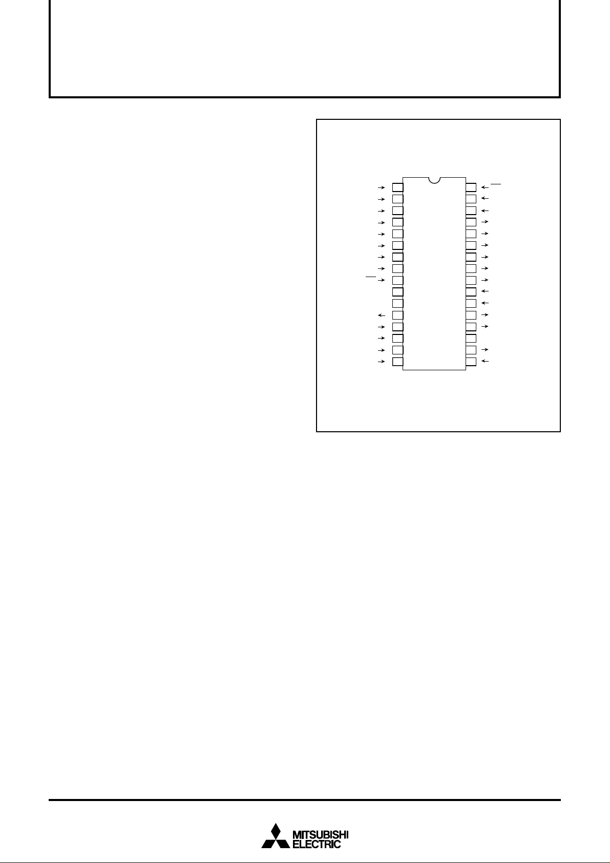
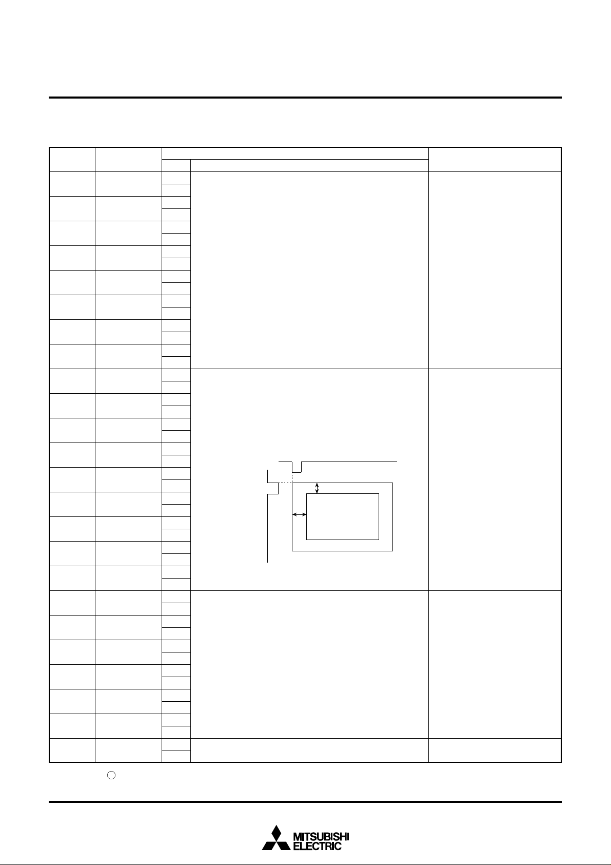
PIN CONFIGURATION (TOP VIEW)
AD0
AD1
AD2
AD3
AD4
AD5
AD6
AD7
AC
V
DD1
V
SS
CVIDEO
LECHA
LEBK
CVIN
HOR
1
2
3
4
5
6
7
8
9
10
11
12
13
14
15
16
M35060-XXXSP
32
CS
SCK
31
30
TESTA
29
P5
P4
28
27
P3
26
P2
25
P1
24
P0
TESTB
23
OSCIN
22
21
OSCOUT
20
LP2
V
DD2
19
18
LP1
17
VREF
Outline 32P4B
PIN DESCRIPTION
Pin name
AD0~AD7
AC
VDD1
VSS
CVIDEO
LECHA
LEBK
CVIN
HOR
VREF
LP1
VDD2
LP2
OSCOUT
OSCIN
TESTB
P0
P1
P2
P3
P4
P5
TESTA
SCK
CS
Parallel data input
Auto-clear input
Power pin
Earthing pin
Composite video
signal output
Character level input
Black level input
Composite video
signal input
Synchronous signal
input
Slice level input
Filter output 1
Power pin
Filter output 2
The pins for attaching an external oscillator circuit for genera-
ting the synchronization signal.
Test input
Port output
Port output
Port output
Port output
Port output
Port output
Test input
Clock input for data
input
Chip select input
Input/Output
Input
Input
—
—
Output
Input
Input
Input
Input
Input
Output
—
Output
Output
Input
Input
Output
Output
Output
Output
Output
Output
Input
Input
Input
MITSUBISHI MICROCOMPUTERS
M35060-XXXSP
SCREEN CHARACTER and PATTERN DISPLAY CONTROLLERS
FunctionSymbol
These input pins determine address and data of the Display RAM, Control RAM, and
Overlay RAM (SYRAM) by 8-bit parallel. Hysteresis input is required.
When this input pin transitions from “H” to “L”, the device is reset. Built-in a pull-up
resistor. Hysteresis input is required.
Digital power supply pin. This pin must be connected to + 5V.
Ground pin. This pin must be connected to 0V.
This pin outputs the composite video signal. The output signal is 2Vp-p. In superim-
pose mode, this pin’s signal consists of the OSD signal combined with the input
composite signal CVIN.
This input pin is used for controlling the “white” character color level of the OSD signal.
This input pin is used for controlling the “black” character color level of the OSD signal.
This input pin is used for the superimpose mode. An external composite signal may be
input through this pin and mixed with the internally generated OSD signal.
This input pin is used to input the same signal as CVIN. The horizontal and vertical
sync signals are then extracted internally within the device.
This input pin is used to determine the slice voltage for extracting the sync signals from
the video composite signal.
This is filter output pin 1.
Analog power supply pin. This pin must be connected to +5V.
This is filter output pin 2.
These are the pins for attaching an external oscillator circuit for generating the
synchronization signal:
NTSC (3.580MHz), PAL (4.434MHz), M-PAL (3.576MHz).
Factory test pin. The pin must be connected to GND.
This output pin can be configured to port P0 or YM output.
This output pin can be configured to port P1 or BLNK output.
This output pin can be configured to port P2 or B output.
This output pin can be configured to port P3 or G output.
This output pin can be configured to port P4 or R output.
This output pin can be configured to port P5 or CSYN output.
Factory test pin. The pin must be connected to GND.
This pin is enabled when the CS pin is “L”. Data input to pins AD0~AD7 is latched at the
rising edge of this signal. This pin is hysteresis input.
This is chip selection input pin. When this pin is “L”, transmission is enabled. This pin is
hysteresis input.
2
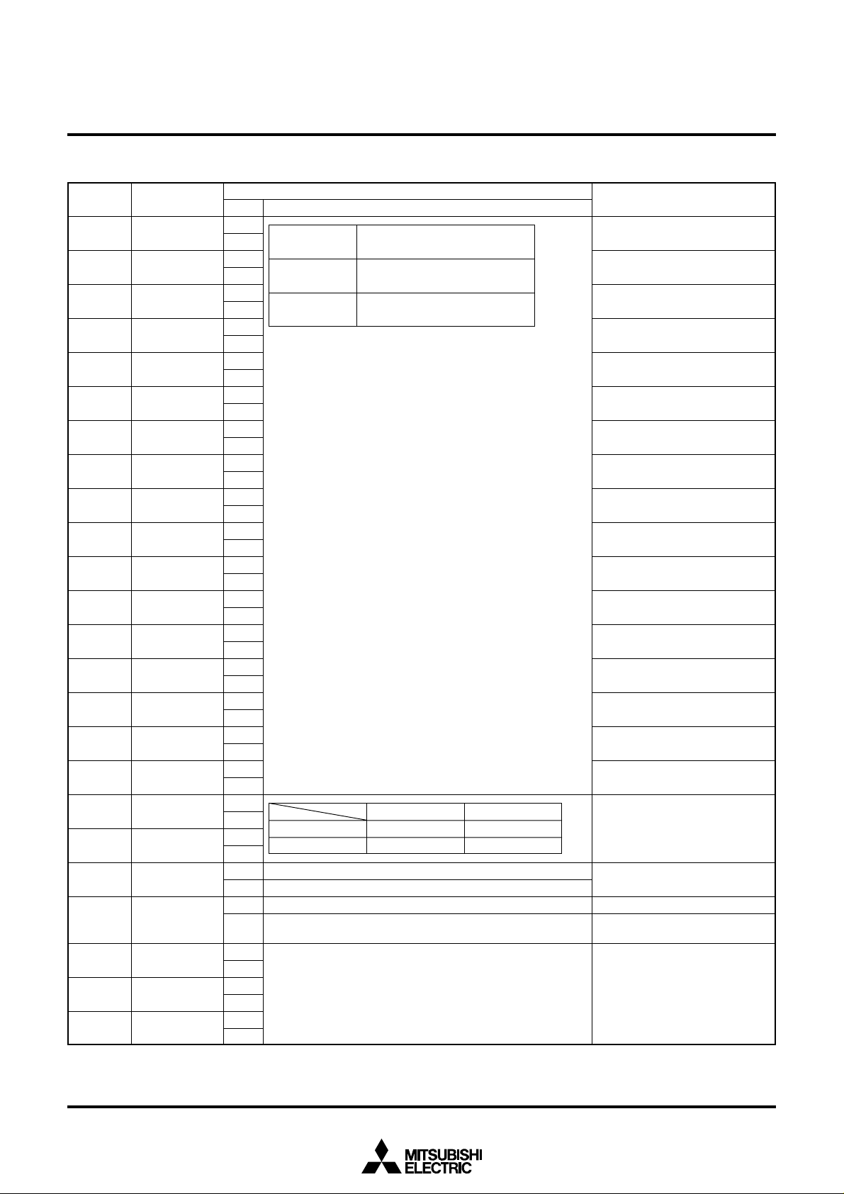
MITSUBISHI MICROCOMPUTERS
Write access
control
Read access
control
Display
position
detection
Timing
generator
Sync
separation
Vsync
separation
Synchronous
correction circuit
Quadruple
frequency circuit
Display control registerDisplay RAM
Character
Pattern ROM
SYRAM
Blinking
Shift
TESTB
CVIN
LEBK
LECHA
CVIDEO
LP1
OSCOUT
OSCIN
LP2
SCK CS
TESTA HOR
VREF
P0
/YM
P1
/BLNK
P2
/B
P3
/G
P4
/R
P5
/CSYN
Port output/Selection
Display control
Sync
generation
Video signal
output
NTSC, PAL,
M-PAL
V
DD2
V
SS
AC
AD0
AD1
AD2
AD3
AD4
AD5
AD6
AD7
3231
30
16 17
18
21
22
20
23
15
14
13
12
29
282726
2524
9
1119
8
7
6
5
4
3
2
1
V
DD1
10
Input control circuit
M35060-XXXSP
SCREEN CHARACTER and PATTERN DISPLAY CONTROLLERS
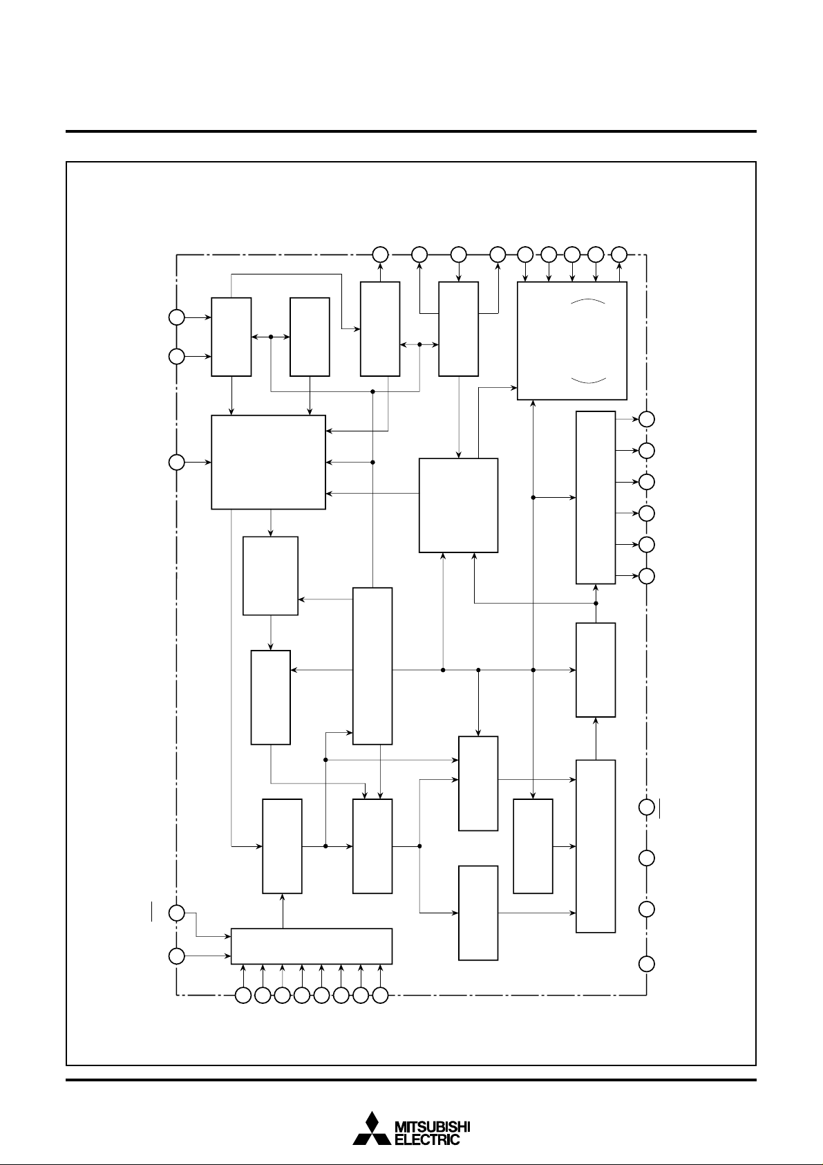
BLOCK DIAGRAM
3
MITSUBISHI MICROCOMPUTERS
M35060-XXXSP
SCREEN CHARACTER and PATTERN DISPLAY CONTROLLERS
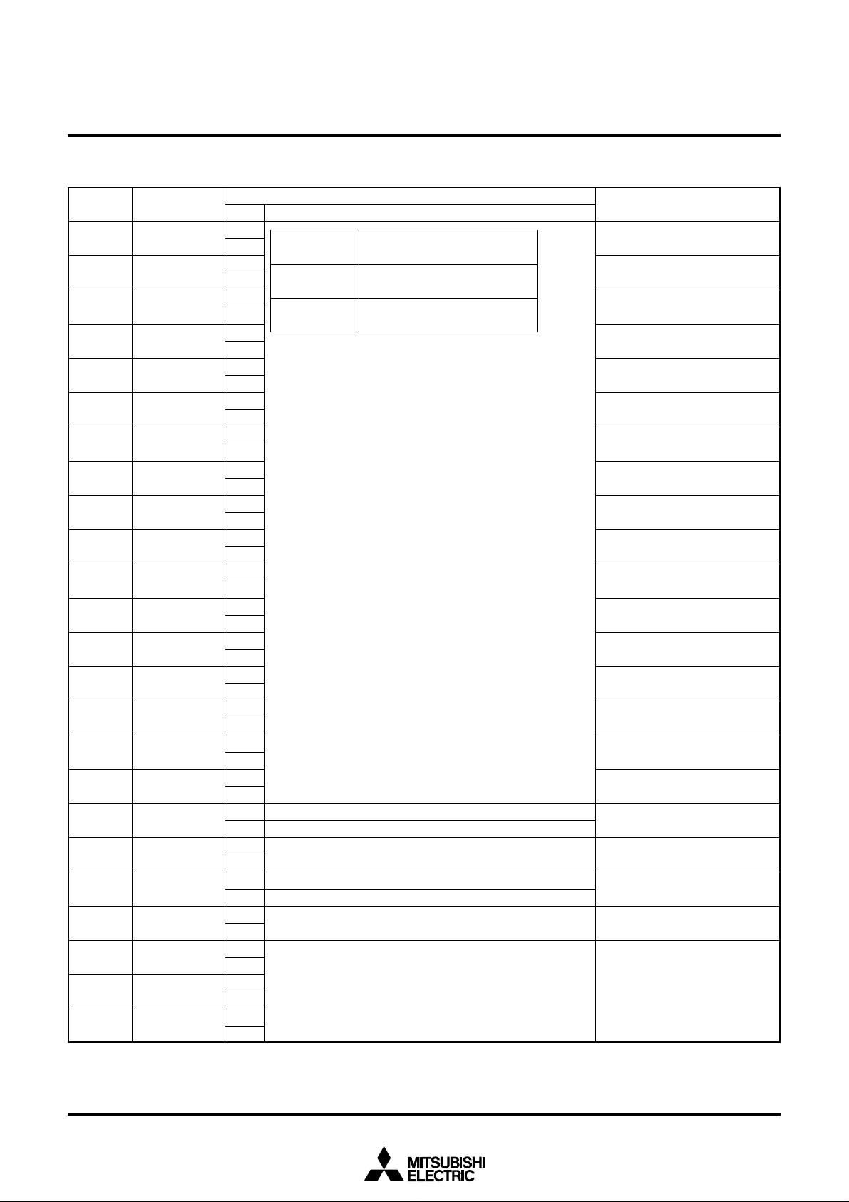
MEMORY CONSTRUCTION
Address 00016 to 2A716 are assigned to the display RAM, 2A816 to
2B016 are assigned to the display control registers and 30016 to
6EC16 are assigned to SYRAM.
Table 1 The memory constitution of display RAM and register
add-
DA17
DA16
DA15
DA14
DA13
ress
000
16
SB
SG
SR
SYC5
~
SY color setting
2A7
16
SB
SG
SR
SYC5
TEST
TEST
2A8
16
–
3
2A9
16
–
–
2AA
16
–
–
2AB
16
–
–
2AC
16
–
–
–
–
PC7
–
TEST
23
–
PC6
TEST
19
2AD
16
2AE
16
2AF
16
2B0
16
TESTn (n = number) is MITSUBISHI test memory. Set 0 to all bits.
2
–
–
TEST
26
–
TEST
22
–
PC5
TEST
18
TEST
1
BLINK
3
TEST
12
TEST
25
TEST
21
SERS
3
–
PC4
TEST
17
DA12
SYC4
SYC3
SYRAM setting
SYC4
SYC3
TEST
TEST
0
11
BLINK
BLINK
2
1
TEST
EQP
20
PHASE
PHASE
2
1
LINE
LINE
B
G
SERS
SERS
2
1
SEND
–
4
PC3
PC2
TEST
LEVEL
24
2
DA11
SYC2
SYC2
TEST
10
BLINK
0
HIDE
PHASE
0
LINE
R
SERS
0
SEND
3
PC1
LEVEL
1
DA10
SYC1
SYC1
HP8
HSZ
16
VSZ
16
DSP0
16
DSP1
16
ERS
16
SEND
2
PC0
LEVEL
0
DAF
DAE
SYC0
BB
Raster color setting
SYC0
BB
HP7
HP6
HSZ
HSZ
15
14
VSZ
VSZ
15
14
DSP0
DSP0
15
14
DSP1
DSP1
15
14
ERS
ERS
15
14
SEND
SEND
1
0
SRAND
ALL24
2
INT
PAL
NON
NTSC
DAD
BG
BG
HP5
HSZ
13
VSZ
13
DSP0
13
DSP1
13
ERS
13
SST
4
SRAND
1
MPAL
The internal circuit is reset and all display control registers (address
2A816 to 2B016) are set to “0”. The memory constitution of display
RAM and register is shown in Figure 1 and the memory constitution
of SYRAM is shown in Figure 2.
DAC
DAB
DAA
DA9
DA8
DA7
DA6
BR
BR
HP4
HSZ
12
VSZ
12
DSP0
12
DSP1
12
ERS
12
SST
3
SRAND
0
PALH
BLINK
CB
CG
BLINK
Character color setting
BLINK
CB
CG
HP3
HP2
HP1
HSZ
HSZ
10
VSZ
10
DSP0
10
DSP1
10
ERS
10
SST
1
PTD
4
TEST
15
HSZ
9
VSZ
9
DSP0
09
DSP1
09
ERS
9
SST
0
PTD
3
SEPV1
11
VSZ
11
DSP0
11
DSP1
11
ERS
11
SST
2
PTD
5
TEST
16
CR
CR
HP0
HSZ
8
VSZ
8
DSP0
08
DSP1
08
ERS
8
SLIN
4
PTD
2
SEPV0
C7
C7
VP7
HSZ
7
VSZ
7
DSP0
07
DSP1
07
ERS
7
SLIN
3
PTD
1
BLK
C6
C6
VP6
HSZ
6
VSZ
6
DSP0
06
DSP1
06
ERS
6
SLIN
2
PTD
0
–
DA5
C5
C5
VP5
HSZ
VSZ
DSP0
05
DSP1
05
ERS
SLIN
PTC
5
DSP
ONV
Character setting
5
5
5
1
DA4
C4
C4
VP4
HSZ
4
VSZ
4
DSP0
04
DSP1
04
ERS
4
SLIN
0
PTC
4
DSP
ON
DA3
C3
C3
VP3
HSZ
3
VSZ
3
DSP0
03
DSP1
03
ERS
3
SBIT
3
PTC
3
–
DA2
C2
C2
VP2
HSZ
2
VSZ
2
DSP0
02
DSP1
02
ERS
2
SBIT
2
PTC
2
SEL
COR
DA1
C1
C1
VP1
HSZ
1
VSZ
1
DSP0
01
DSP1
01
ERS
1
SBIT
1
PTC
1
–
DA0
C0
C0
VP0
HSZ
0
VSZ
0
DSP0
00
DSP1
00
ERS
0
SBIT
0
PTC
0
EX
Table 2 The memory constitution of SYRAM
address
300
16
DA17 ~ DAD
DAC
SYEX
DAB
S00B
DAA
S00A
DA9
S009
0
30C
310
16
16
SYEX
SYEX
S00B
S01B
S00A
S01A
S009
S019
0
31C
6D0
6DC
6E0
16
~~~~~
16
…
0
16
16
SYEX
……………
SYEX
SYEX
SYEX
S01B
S3DB
…………
S3DB
S3EB
S01A
S3DA
…………
S3DA
S3EA
S019
S3D9
…………
S3D9
S3E9
0
6EC
16
: Name or value changes by definite ratio.
~
: The same name or value continues.
…
SYEX
S3EB
S3EA
S3E9
DA8
S008
S008
S018
S018
S3D8
…………
S3D8
S3E8
S3E8
DA7
S007
S007
S017
S017
S3D7
……………………
S3D7
S3E7
S3E7
DA6
S006
S006
S016
S016
S3D6
…………
S3D6
S3E6
S3E6
DA5
S005
S005
S015
S015
~
S3D5
S3D5
S3E5
S3E5
DA4
S004
DA3
S003
DA2
S002
DA1
S001
DA0
S000
SYRAM code
0016
S004
S014
S003
S013
S002
S012
S001
S011
S000
S010
0116
S014
S013
S012
S011
S010
~
S3D4
…………
S3D3
…………
S3D4
S3E4
S3E4
…………
S3D3
S3E3
S3E3
S3D2
…………
S3D2
S3E2
S3E2
S3D1
…………
S3D1
S3E1
S3E1
S3D0
…………
S3D0
S3E0
S3E0
3D16
3E16
4
SCREEN CHARACTER and PATTERN DISPLAY CONTROLLERS
Line 16
001
002
003
004
005
006
007
008
009
00A
00B
00C
00D
00E
00F
010
011
012
013
014
015
016
017
018
019
01A
01B
01C
01D
01E
01F
020
021
022
023
024
025
026
027
000
079
07A
07B
07C
07D
07E
07F
080
081
082
083
084
085
086
087
088
089
08A
08B
08C
08D
08E
08F
090
091
092
093
094
095
096
097
098
099
09A
09B
09C
09D
09E
09F
078
0A1
0A2
0A3
0A4
0A5
0A6
0A7
0A8
0A9
0AA
0AB
0AC
0AD
0AE
0AF
0B0
0B1
0B2
0B3
0B4
0B5
0B6
0B7
0B8
0B9
0BA
0BB
0BC
0BD
0BE
0BF
0C0
0C1
0C2
0C3
0C4
0C5
0C6
0C7
0A0
0C9
0CA
0CB
0CC
0CD
0CE
0CF
0D0
0D1
0D2
0D3
0D4
0D5
0D6
0D7
0D8
0D9
0DA
0DB
0DC
0DD
0DE
0DF
0E0
0E1
0E2
0E3
0E4
0E5
0E6
0E7
0E8
0E9
0EA
0EB
0EC
0ED
0EE
0EF
0C8
0F1
0F2
0F3
0F4
0F5
0F6
0F7
0F8
0F9
0FA
0FB
0FC
0FD
0FE
0FF
100
101
102
103
104
105
106
107
108
109
10A
10B
10C
10D
10E
10F
110
111
112
113
114
115
116
117
0F0
141
142
143
144
145
146
147
148
149
14A
14B
14C
14D
14E
14F
150
151
152
153
154
155
156
157
158
159
15A
15B
15C
15D
15E
15F
160
161
162
163
164
165
166
167
140
169
16A
16B
16C
16D
16E
16F
170
171
172
173
174
175
176
177
178
179
17A
17B
17C
17D
17E
17F
180
181
182
183
184
185
186
187
188
189
18A
18B
18C
18D
18E
18F
168
1B9
1BA
1BB
1BC
1BD
1BE
1BF
1C0
1C1
1C2
1C3
1C4
1C5
1C6
1C7
1C8
1C9
1CA
1CB
1CC
1CD
1CE
1CF
1D0
1D1
1D2
1D3
1D4
1D5
1D6
1D7
1D8
1D9
1DA
1DB
1DC
1DD
1DE
1DF
1B8
259
25A
25B
25C
25D
25E
25F
260
261
262
263
264
265
266
267
268
269
26A
26B
26C
26D
26E
26F
270
271
272
273
274
275
276
277
278
279
27A
27B
27C
27D
27E
27F
258
119
11A
11B
11C
11D
11E
11F
120
121
122
123
124
125
126
127
128
129
12A
12B
12C
12D
12E
12F
130
131
132
133
134
135
136
137
138
139
13A
13B
13C
13D
13E
13F
118
191
192
193
194
195
196
197
198
199
19A
19B
19C
19D
19E
19F
1A0
1A1
1A2
1A3
1A4
1A5
1A6
1A7
1A8
1A9
1AA
1AB
1AC
1AD
1AE
1AF
1B0
1B1
1B2
1B3
1B4
1B5
1B6
1B7
190
1E1
1E2
1E3
1E4
1E5
1E6
1E7
1E8
1E9
1EA
1EB
1EC
1ED
1EE
1EF
1F0
1F1
1F2
1F3
1F4
1F5
1F6
1F7
1F8
1F9
1FA
1FB
1FC
1FD
1FE
1FF
200
201
202
203
204
205
206
207
1E0
231
232
233
234
235
236
237
238
239
23A
23B
23C
23D
23E
23F
240
241
242
243
244
245
246
247
248
249
24A
24B
24C
24D
24E
24F
250
251
252
253
254
255
256
257
230
281
282
283
284
285
286
287
288
289
28A
28B
28C
28D
28E
28F
290
291
292
293
294
295
296
297
298
299
29A
29B
29C
29D
29E
29F
2A0
2A1
2A2
2A3
2A4
2A5
2A6
2A7
280
051
052
053
054
055
056
057
058
059
05A
05B
05C
05D
05E
05F
060
061
062
063
064
065
066
067
068
069
06A
06B
06C
06D
06E
06F
070
071
072
073
074
075
076
077
050
029
02A
02B
02C
02D
02E
02F
030
031
032
033
034
035
036
037
038
039
03A
03B
03C
03D
03E
03F
040
041
042
043
044
045
046
047
048
049
04A
04B
04C
04D
04E
04F
028
208
209
20A
20B
20C
20D
20E
20F
210
211
212
213
214
215
216
217
218
219
21A
21B
21C
21D
21E
21F
220
221
222
223
224
225
226
227
228
229
22A
22B
22C
22D
22E
22F
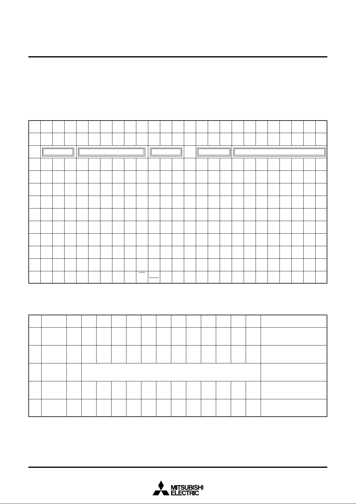
Row
The hexadecimal numbers in the boxes show the display RAM address
Line 0
Line 1
Line 15
SCREEN CONSTITUTION
The screen lines and rows are determined from each address of the display RAM.
The screen constitution is shown in Figure 1.
MITSUBISHI MICROCOMPUTERS
M35060-XXXSP
Fig. 1 Screen constitution
5
REGISTERS DESCRIPTION
(1) Address 2A816
DA
0
1
2
3
4
5
6
7
8
9
A
B
C
D
E
F
10
11
12
13
14
15
16
17
Register
VP0
VP1
VP2
VP3
VP4
VP5
VP6
VP7
HP0
HP1
HP2
HP3
HP4
HP5
HP6
HP7
HP8
TEST10
TEST11
TEST0
TEST1
TEST2
TEST3
—
Status
0
1
0
1
0
1
0
1
0
1
0
1
0
1
0
1
0
1
0
1
0
1
0
1
0
1
0
1
0
1
0
1
0
1
0
1
0
1
0
1
0
1
0
1
0
1
0
1
SCREEN CHARACTER and PATTERN DISPLAY CONTROLLERS
Contents
Function
If VS is the vertical display start location,
VS = H ✕ ( Σ 2n VPn )
If HS is the horizontal display start location,
HS = T ✕ ( Σ 2n HPn + 9 )
Test mode (Must be cleared to 0.)
Must be cleared to 0.
7
n=0
H: Cycle with the horizontal synchronizing pulse
8
n=0
T: Cycle with the display clock
HOR
VS
HS
Character
displaying area
VERT
1 bit weights 1 clock.
MITSUBISHI MICROCOMPUTERS
M35060-XXXSP
Remarks
The vertical start location is
specified using the 8 bits from
VP7 to VP0.
VP7 to VP0 < 1416 are not
available.
The horizontal start location is
specified using the 9 bits from
HP8 to HP0.
HP8 to HP0 < 1916 are not
available.
TV screen
Note: The mark around the status value means the reset status by the “L” level is input to AC pin.
6
(2) Address 2A916
DA Register
0
1
2
3
4
5
6
7
8
9
A
B
C
D
E
F
10
11
12
13
14
15
16
17
HSZ0
HSZ1
HSZ2
HSZ3
HSZ4
HSZ5
HSZ6
HSZ7
HSZ8
HSZ9
HSZ10
HSZ11
HSZ12
HSZ13
HSZ14
HSZ15
HSZ16
BLINK0
BLINK1
BLINK2
BLINK3
—
—
—
SCREEN CHARACTER and PATTERN DISPLAY CONTROLLERS
Contents
Status
0
1
0
1
0
1
0
1
0
1
0
1
0
1
0
1
0
1
0
1
0
1
0
1
0
1
0
1
0
1
0
1
0
1
0
1
0
1
0
1
0
1
0
1
0
1
0
1
HSZx
0
1
BLINK1
0
1
Cycle approximately 1 second.
Cycle approximately 0.5 second.
Normal blinking
Normal character, reversed character alternation display.
Must be cleared to 0.
Horizontal direction character size
BLINK0
Function
1T/dot
2T/dot
0
Blinking OFF
Duty 50%
T: Display clock
1
Duty 25%
Duty 75%
MITSUBISHI MICROCOMPUTERS
M35060-XXXSP
Remarks
Set to line 0 of display RAM
Set to line 1 of display RAM
Set to line 2 of display RAM
Set to line 3 of display RAM
Set to line 4 of display RAM
Set to line 5 of display RAM
Set to line 6 of display RAM
Set to line 7 of display RAM
Set to line 8 of display RAM
Set to line 9 of display RAM
Set to line 10 of display RAM
Set to line 11 of display RAM
Set to line 12 of display RAM
Set to line 13 of display RAM
Set to line 14 of display RAM
Set to line 15 of display RAM
Set to line 16 of display RAM
Blinking duty ratio can be altered.
Blinking cycle can be altered.
Character is in flashing state.
Character is always displayed
(normal character, reversed character).
7
(3) Address 2AA16
MITSUBISHI MICROCOMPUTERS
M35060-XXXSP
SCREEN CHARACTER and PATTERN DISPLAY CONTROLLERS
DA Register
0
1
2
3
4
5
6
7
8
9
A
B
C
D
E
F
10
11
12
13
14
15
16
17
VSZ0
VSZ1
VSZ2
VSZ3
VSZ4
VSZ5
VSZ6
VSZ7
VSZ8
VSZ9
VSZ10
VSZ11
VSZ12
VSZ13
VSZ14
VSZ15
VSZ16
HIDE
TEST20
EQP
TEST12
—
—
—
Status
0
1
0
1
0
1
0
1
0
1
0
1
0
1
0
1
0
1
0
1
0
1
0
1
0
1
0
1
0
1
0
1
0
1
0
1
0
1
0
1
0
1
0
1
0
1
0
1
VSZx
0
1
SYRAM writting over
SYRAM writting over or character erasing
Test mode (Must be cleared to 0.)
It does not include equivalent pulse.
It includes equivalent pulse.
Test mode (Must be cleared to 0.)
Must be cleared to 0.
Vertical direction character size
H: Horizontal synchronous pulse
Contents
Function
1H/dot
2H/dot
Remarks
Set to line 0 of display RAM
Set to line 1 of display RAM
Set to line 2 of display RAM
Set to line 3 of display RAM
Set to line 4 of display RAM
Set to line 5 of display RAM
Set to line 6 of display RAM
Set to line 7 of display RAM
Set to line 8 of display RAM
Set to line 9 of display RAM
Set to line 10 of display RAM
Set to line 11 of display RAM
Set to line 12 of display RAM
Set to line 13 of display RAM
Set to line 14 of display RAM
Set to line 15 of display RAM
Set to line 16 of display RAM
Decided by register LINER, G and
B or DAC bit of SYRAM.
8
(4) Address 2AB16
DA Register
0
1
2
3
4
5
6
7
8
9
A
B
C
D
E
F
10
11
12
13
14
15
16
17
DSP0 00
DSP0 01
DSP0 02
DSP0 03
DSP0 04
DSP0 05
DSP0 06
DSP0 07
DSP0 08
DSP0 09
DSP0 10
DSP0 11
DSP0 12
DSP0 13
DSP0 14
DSP0 15
DSP0 16
PHASE 0
PHASE 1
PHASE 2
TEST25
TEST26
MITSUBISHI MICROCOMPUTERS
M35060-XXXSP
SCREEN CHARACTER and PATTERN DISPLAY CONTROLLERS
Contents
Status
0
1
0
1
0
1
0
1
0
1
0
1
0
1
0
1
0
1
0
1
0
1
0
1
0
1
0
1
0
1
0
1
0
1
0
1
0
1
0
1
0
1
0
1
—
—
0
1
0
1
DSP0XX
DSP1XX
0
1
Set by combination of DSP0XX (address 2AB16 and DSP1XX)
and DSP1XX (address 2AC16).
At internal synchronous mode (EX = 1), display monitor signal
area is all blanking signal (BLNK output) area.
Note: For halftone display, it is necessary to input the external
composite video signal to the CVIN terminal, and externally
connect a 100 to 200 resistor in series.
However, the halftone display is possible only with
superimposed displays.
PHASE
PHASE
PHASE
2
0
0
0
0
1
1
1
1
Test mode (Must be cleared to 0.)
Must be cleared to 0.
0
1
0
0
1
0
0
1
1
1
0
0
1
0
0
1
1
1
Function
0
Character
Matrix-outline
SELCOR=0
Black
Red
Green
Yellow
Blue
Magenta
Cyan
White
1
Border
Halftone
(Note)
Color
SELCOR=1
Black
Red–2
Green–2
Yellow
Gray
Yellow–2
Cyan
White
Set to line 0 of display RAM
Set to line 1 of display RAM
Set to line 2 of display RAM
Set to line 3 of display RAM
Set to line 4 of display RAM
Set to line 5 of display RAM
Set to line 6 of display RAM
Set to line 7 of display RAM
Set to line 8 of display RAM
Set to line 9 of display RAM
Set to line 10 of display RAM
Set to line 11 of display RAM
Set to line 12 of display RAM
Set to line 13 of display RAM
Set to line 14 of display RAM
Set to line 15 of display RAM
Set to line 16 of display RAM
Raster color setting.
Refer Fig 3, 4 about phase angle.
Remarks
9

(5) Address 2AC16
DA Register
0
1
2
3
4
5
6
7
8
9
A
B
C
D
E
F
10
11
12
13
14
15
16
17
DSP1 00
DSP1 01
DSP1 02
DSP1 03
DSP1 04
DSP1 05
DSP1 06
DSP1 07
DSP1 08
DSP1 09
DSP1 10
DSP1 11
DSP1 12
DSP1 13
DSP1 14
DSP1 15
DSP1 16
TEST21
LINER
LINEG
LINEB
—
—
—
SCREEN CHARACTER and PATTERN DISPLAY CONTROLLERS
Contents
Status
0
1
0
1
0
1
0
1
0
1
0
1
0
1
0
1
0
1
0
1
0
1
0
1
0
1
0
1
0
1
0
1
0
1
0
1
0
1
0
1
0
1
0
1
0
1
0
1
DSP0XX
DSP1XX
0
1
Set by combination of DSP0XX (address 2AB16 and DSP1XX)
and DSP1XX (address 2AC16).
At internal synchronous mode (EX = 1), display monitor signal
area is all blanking signal (BLNK output) area.
Note: For halftone display, it is necessary to input the external
composite video signal to the CVIN terminal, and externally
connect a 100 to 200 resistor in series.
However, the halftone display is possible only with
superimposed displays.
LINE
LINE
LINE
B
0
0
0
0
1
1
1
1
Test mode (Must be cleared to 0.)
Must be cleared to 0.
R
G
0
0
1
0
0
1
1
1
0
0
1
0
0
1
1
1
Function
0
Character
Matrix-outline
SELCOR=0
Black
Red
Green
Yellow
Blue
Magenta
Cyan
White
1
Border
Halftone
(Note)
Color
SELCOR=1
Black
Red–2
Green–2
Yellow
Gray
Yellow–2
Cyan
White
MITSUBISHI MICROCOMPUTERS
M35060-XXXSP
Remarks
Set to line 0 of display RAM
Set to line 1 of display RAM
Set to line 2 of display RAM
Set to line 3 of display RAM
Set to line 4 of display RAM
Set to line 5 of display RAM
Set to line 6 of display RAM
Set to line 7 of display RAM
Set to line 8 of display RAM
Set to line 9 of display RAM
Set to line 10 of display RAM
Set to line 11 of display RAM
Set to line 12 of display RAM
Set to line 13 of display RAM
Set to line 14 of display RAM
Set to line 15 of display RAM
Set to line 16 of display RAM
SYRAM color setting.
Color is decided by DAC bit
(SYEX) of SYRAM or HIDE
register.
Refer Fig. 3, 4 about phase angle.
10
(6) Address 2AD16
MITSUBISHI MICROCOMPUTERS
M35060-XXXSP
SCREEN CHARACTER and PATTERN DISPLAY CONTROLLERS
DA Register
0
1
2
3
4
5
6
7
8
9
A
B
C
D
E
F
10
11
12
13
14
15
16
17
ERS0
ERS1
ERS2
ERS3
ERS4
ERS5
ERS6
ERS7
ERS8
ERS9
ERS10
ERS11
ERS12
ERS13
ERS14
ERS15
ERS16
SERS0
SERS1
SERS2
SERS3
TEST22
TEST23
—
Contents
Status
0
Erase display RAM
1
0
1
0
1
0
1
0
1
0
1
0
1
0
1
0
1
0
1
0
1
0
1
0
1
0
1
0
1
0
1
0
1
0
1
0
1
0
1
0
1
0
1
0
1
0
1
ERSx
0
1
It is unnecessary to reset these registers to “0”.
Multiple settings of ERSn is not allowed.
Erase SYRAM
SERSx
0
1
It is unnecessary to reset these registers to “0”.
Multiple settings of SERSn is not allowed.
Test mode (Must be cleared to 0.)
Must be cleared to 0.
Function
SYRAM erase
RAM erase
do erase
do not erase
do erase
do not erase
Remarks
Set to line 0 of display RAM
Set to line 1 of display RAM
Set to line 2 of display RAM
Set to line 3 of display RAM
Set to line 4 of display RAM
Set to line 5 of display RAM
Set to line 6 of display RAM
Set to line 7 of display RAM
Set to line 8 of display RAM
Set to line 9 of display RAM
Set to line 10 of display RAM
Set to line 11 of display RAM
Set to line 12 of display RAM
Set to line 13 of display RAM
Set to line 14 of display RAM
Set to line 15 of display RAM
Set to line 16 of display RAM
Set to SYRAM code 0016 ~ 0F16
Set to SYRAM code 1016 ~ 1F16
Set to SYRAM code 2016 ~ 2F16
Set to SYRAM code 3016 ~ 3E16
11
(7) Address 2AE16
DA
0
1
2
3
4
5
6
7
8
9
A
B
C
D
E
F
10
11
12
13
14
15
16
17
Note: When the scrolling on, set the ratio which will be SC < SB < SD.
Register
SBIT0
SBIT1
SBIT2
SBIT3
SLIN0
SLIN1
SLIN2
SLIN3
SLIN4
SST0
SST1
SST2
SST3
SST4
SEND0
SEND1
SEND2
SEND3
SEND4
—
—
—
—
—
Status
0
Set display start bit of scroll block:
1
0
1
3
SA = Σ 2n (SBITn)
n=0
0
1
0
1
0
Set display start line of scroll block:
1
0
1
4
SB = Σ 2n (SLINn)
n=0
0
1
0
1
0
1
0
Set start line of scroll block
1
(last line number of the fixed block 1):
0
1
4
SC = Σ 2n (SSTn)
n=0
0
1
0
1
0
1
0
Set start line of fixed block 2
1
(last line number of the scroll block):
0
1
0
4
SD = Σ 2n (SENDn)
n=0
1
0
1
0
1
0
Must be cleared to 0.
1
0
1
0
1
0
1
0
1
MITSUBISHI MICROCOMPUTERS
M35060-XXXSP
SCREEN CHARACTER and PATTERN DISPLAY CONTROLLERS
Contents
Function
Setting valid
invalid
Setting valid
invalid
Setting valid
invalid
When the scrolling on
setting valid SD = 2 to 17
invalid SD = 18 to 31
When the scrolling off
set SD = 0
SD > SC + 2
Remarks
SA = 0 to 12
SA = 13 to 15
SB = 0 to 16
SB = 17 to 31
SC = 0 to 15
SC = 16 to 31
12

SCREEN CHARACTER and PATTERN DISPLAY CONTROLLERS
(8) Address 2AF16
DA Register
0
1
2
3
4
5
6
7
8
9
A
B
C
D
E
F
10
11
12
13
14
15
16
17
Note: At EX (address 2B016) = “0” (external synchronous), setting “1” of ALL24 register is not available.
Refer Fig. 2 about PTC0 ~ 5, PTD0 ~ 5.
PTC0
PTC1
PTC2
PTC3
PTC4
PTC5
PTD0
PTD1
PTD2
PTD3
PTD4
PTD5
SRAND0
SRAND1
SRAND2
ALL24
PC0
PC1
PC2
PC3
PC4
PC5
PC6
PC7
Status
0
Port P0 output
1
YM output
0
Port P1 output
1
BLNK output
0
Port P2 output
1
B output
0
Port P3 output
1
G output
0
Port P4 output
1
R output
0
Port P5 output
1
CSYN output
0
When port output: 0 output, when YM output: negative polarity.
1
When port output: 1 output, when YM output: polarity.
0
When port output: 0 output, when BLNK output: negative polarity.
1
When port output: 1 output, when BLNK output: polarity.
0
When port output: 0 output, when B output: negative polarity.
1
When port output: 1 output, when B output: polarity.
0
When port output: 0 output, when G output: negative polarity.
1
When port output: 1 output, when G output: polarity.
0
When port output: 0 output, when R output: negative polarity.
1
When port output: 1 output, when R output: polarity.
0
When port output: 0 output, when CSYN output: negative polarity.
1
When port output: 1 output, when CSYN output: polarity.
0
SRAND1SRAND
1
0
1
0
1
Vertical direction is 1 dot only.
Blanking with all 40 characters in matrix-outline mode
0
Horizontal display period fully blanked with all characters in
1
matrix-outline size.
0
Display frequency fT control
1
0
fT = fH ✕ { Σ (2nPCn) + 512 }
1
0
1
0
1
0
1
0
1
0
1
0
1
0
0
0
0
1
1
0
1
1
7
n=0
Contents
Function
SRAND2
0
Complete border = 1 dot
Complete border = 2 dot
Complete border = 3 dot
Complete border = 4 dot
Right and dot border = 1 dot
Right and dot border = 2 dot
Right and dot border = 3 dot
Right and dot border = 4 dot
MITSUBISHI MICROCOMPUTERS
M35060-XXXSP
Remarks
Select P0 pin
Select P1 pin
Select P2 pin
Select P3 pin
Select P4 pin
Select P5 pin
Select data of P0 pin
Select data of P1 pin
Select data of P2 pin
Select data of P3 pin
Select data of P4 pin
Select data of P5 pin
1
Condition of border display is
changeable.
Horizontal display range can be
altered when all characters are in
matrix-outline size.
At external synchronous, set to 0.
Operation of character code FF16
becomes ineffective.
PC7 ~ PC0 < 3616,
PC7 ~ PC0 > C616 is not
available.
13

MITSUBISHI MICROCOMPUTERS
M35060-XXXSP
SCREEN CHARACTER and PATTERN DISPLAY CONTROLLERS
(9) Address 2B016
DA Register
0
1
2
3
4
5
6
7
8
9
A
B
C
D
E
F
10
11
12
13
14
15
16
17
Note: For internal synchronization, shut out (mute) the external video signal input to the CVIN terminal, outside the IC. This avoids external video signal leaks
inside the IC.
EX
—
SELCOR
—
DSPON
DSPONV
—
BLK
SEPV0
SEPV1
TEST15
TEST16
PALH
MPAL
PAL/NTSC
INT/NON
LEVEL0
LEVEL1
LEVEL2
TEST24
TEST17
TEST18
TEST19
—
Status
0
External synchronization
1
Internal synchronization
0
Set to “0”.
1
0
Normal
1
Mode of expansion
0
Must be cleared to 0.
1
0
Digital output display OFF
1
Digital output display ON
0
Composite video output display OFF
1
Composite video output display ON
0
Must be cleared to 0.
1
0
Matrix outline
1
Matrix outline + border
0
SEPV1
SEPV0
0
0
1
0
0
1
1
1
0
Test mode (Must be cleared to 0.)
1
0
1
0
Interlace/noninterlace normal mode
1
Interlace/noninterlace expansion mode
0
PAL/NTSC
1
0
1
Interlace
0
Noninterlace
1
Composite video generation is off.
0
Composite video generation is on.
1
Display clock is on (oscillating).
0
Display clock is off (not oscillating).
1
Sync separation is disabled.
0
Sync separation is enabled.
1
Test mode (Must be cleared to 0.)
0
1
0
1
0
1
0
1
Must be cleared to 0.
0
1
Separation is performed during (1) in vertical blanking period
1
Separation is performed during (2) in vertical blanking period 1
0
Separation is performed during (3) in vertical blanking period
1
Unavailable
0
0
1
1
Contents
Function
Composite Sync Spearation Function
MPAL
0
1
0
1
Format
NTSC
M-PAL
PAL
unavailable
Remarks
(Note)
Refer to Table 3, 4, 7 and 8.
Only at register “DSP1XX”
= 1 (XX = 00 to 16) is available.
Method of sync separation from composite video.
2
3
Case (1) condition: vertical sync must repeat 2X
within (2) or (3); indicates this area.
Only at PAL and MPAL mode are
available.
Refer to Table 5 and 6.
1
14

REGISTER CONSTRUCTION COMPOSITION
MITSUBISHI MICROCOMPUTERS
M35060-XXXSP
SCREEN CHARACTER and PATTERN DISPLAY CONTROLLERS
Table 3 Color and phase of NTSC, PAL (SELCOR = 0)
PHASE2
Table 4 Color and phase of NTSC, PAL (SELCOR = 1)
PHASE2
/
LINEB
0
0
0
0
1
1
1
1
/
LINEB
0
0
0
0
1
1
1
1
PHASE1
/
LINEG
0
0
1
1
0
0
1
1
PHASE1
/
LINEG
0
0
1
1
0
0
1
1
PHASE0
/
LINER
0
1
0
1
0
1
0
1
PHASE0
/
LINER
0
1
0
1
0
1
0
1
Phase (rad)
NTSC
—
7 /16
27 /16
/16
17 /16
11/16
23 /16
—
Phase (rad)
NTSC
—
7 /16
27 /16
/16
—
/16
23 /16
—
PAL
—
± 7 /16
±
5 /16
± /16
±
15 /16
± 11 /16
±
9 /16
—
PAL
—
± 7 /16
±
5 /16
± /16
—
± /16
±
9 /16
—
Color
Black
Red
Green
Yellow
Blue
Magenta
Cyan
White
Color
Black
Red-2
Green-2
Yellow
Gray
Yellow-2
Cyan
White
R (G, B, YM, BLNK, CSYN)
Fig. 2 Switching port output with R, G and B output
Table 5 Setting condition at LEVEL 0, 1 and 2
At display clock operates
LEVEL1
DSPON
DSPONV
CS pin
No character display at display clock
Table 6 Setting condition at LEVEL 0, 1 and 2 (at operation)
LEVEL0
LEVEL1
LEVEL2
0
1
1
L
Operation state
1
0
1
PTD
1
0
Polarity
PTD
PTC
1
0
Select
At display clock stops
1
0
0
H
Stop state
0
1
0
Table 7 Video signal level (SELCOR = 0)
Color name
Sync
Pedestal
Color Burst
Black
Red
Green
Yellow
Blue
Mazenta
Cyan
White
NTSC
7 /16 ± 2 /16
27 /16 ± 2 /16
/16 ± 2 /16
17 /16 ± 2 /16
11/16 ± 2 /16
23 /16 ± 2 /16
Phase (rad) Luminance level (V)
—
—
0
—
—
PAL
—
—
±4 /16
—
± 7 /16 ± 2 /16
±
5 /16 ± 2 /16
± /16 ± 2 /16
±
15 /16 ± 2 /16
± 11 /16 ± 2 /16
±
9 /16 ± 2 /16
—
Min.
1.3
1.9
1.9
2.1
2.3
2.7
3.1
2.0
2.5
2.9
3.1
Typ.
1.5
2.1
2.1
2.3
2.5
2.9
3.3
2.2
2.7
3.1
3.3
Max.
1.7
2.3
2.3
2.5
2.7
3.1
3.5
2.4
2.9
3.3
3.5
Chroma amplitude (vs. color burst)
Min.
—
—
—
—
1.5
1.4
1.0
1.0
1.4
1.5
—
Typ.
—
—
1.0
—
3.0
2.8
2.0
2.0
2.8
3.0
—
Max.
—
—
—
—
4.5
4.2
3.0
3.0
4.2
4.5
—
15

Table 8 Video signal level (SELCOR = 1)
Scanning
(1)Character size
BLNK
R,G,B
YM
CVIDEO
(Internal sync)
12 dots
a: External display
signal
b: Background color
c: Character color
aa
(External sync)
c
b
c
b
13
dots
L
(2)Border size
12 dots
aa
c
b
c
b
(4)Halftone size
14 dots
c
b
c
b
bb
(3)Matrix-outline size
14 dots
c
b
c
b
bb
L
aa
Color name
Sync
Pedestal
Color Burst
Black
Red-2
Green-2
Yellow
Gray
Yellow-2
Cyan
White
NTSC
7 /16 ± 2 /16
27 /16 ± 2 /16
/16 ± 2 /16
/16 ± 2 /16
23 /16 ± 2 /16
Phase (rad) Luminance level (V)
—
—
0
—
—
—
PAL
—
—
±4 /16
—
± 7 /16 ± 2 /16
±
5 /16 ± 2 /16
± /16 ± 2 /16
—
± /16 ± 2 /16
±
9 /16 ± 2 /16
—
MITSUBISHI MICROCOMPUTERS
M35060-XXXSP
SCREEN CHARACTER and PATTERN DISPLAY CONTROLLERS
Chroma amplitude (vs. color burst)
Min.
1.3
1.9
1.9
2.1
2.6
3.1
3.1
2.8
3.2
2.9
3.1
Typ.
1.5
2.1
2.1
2.3
2.8
3.3
3.3
3.0
3.4
3.1
3.3
Max.
1.7
2.3
2.3
2.5
3.0
3.5
3.5
3.2
3.6
3.3
3.5
Min.
—
—
—
—
1.5
0.5
1.0
—
0.4
1.5
—
Typ.
—
—
1.0
—
2.0
1.0
2.0
—
0.8
3.0
—
Max.
—
—
—
—
3.0
1.5
3.0
—
1.2
4.5
—
DISPLAY FORMS
1. Blanking mode
Display forms are shown in T able 9, display forms at each display
mode are shown in Fig. 3.
Table 9 Display forms
Display mode
Character
Border
Matrix-outline
Halftone
DSP1 XX
(Address 2AC16)
DSP0 XX
(Address 2AB16)
0
0
1
1
0
1
0
1
BLNK output
Character size
Border size
All blanking
Blanking OFF
Fig. 3 Display forms at each display mode
16

MITSUBISHI MICROCOMPUTERS
M35060-XXXSP
SCREEN CHARACTER and PATTERN DISPLAY CONTROLLERS
For matrix and halftone, a character’s number of dots in the horizontal direction increases to 14.
Figure 4 shows a display example for a case where adjacent characters have different background colors and for character code FF16.
13 dots 12 dots 13 dots 11 dots 14 dots11 dots 11 dots
40 characters
Character code FF
Fig. 4 Number of dots in the horizontal direction at matrix-outline or halftone
2. Border mode
In border mode, characters are displayed with borders. (Refer to
T able 9.) In matrix and halftone modes also, characters are displayed
with borders if the BLK register (address 2B016) is set to 1.
Table 10 lists the types of borders.
Table 10 Bordering
SRAND2
(Address 2AF
SRAND1, 0
16)
0
The zero
dot
1dot in horizontal
direction
00
01 10 11
2 dots in horizontal
direction
16
3 dots in horizontal
direction
4 dots in horizontal
direction
1
1 dot in horizontal
direction
Horizontal direction bordering is only 1 dot. When the character extends to the top line of the matrix, no border is left at the top, and when the
character extends to the bottom (12th) line of the matrix, no border is left at the bottom.
2 dots in horizontal
direction
3 dots in horizontal
direction
4 dots in horizontal
direction
17

3. Setting matrix outline
The ALL24 register (address 2AF16) allows you to set a matrix outline. A matrix outline can be set for each line by using the DSP1XX
register (address 2AC16) .
However, this setting is inhibited if the EX register (address 2B016)
is 0 (external sync). An example of how you set a matrix outline is
shown in Figure 5.
Setting example of register
DSP1xx
DSP1 00
DSP1 08
DSP1 09
DSP1 10
DSP1 16
.....
.....
“0”
“0”
“1”
“0”
Line 9
“0”
ALL24
“0”
to characters all matrix-outline
40 characters
OSD display area
MITSUBISHI MICROCOMPUTERS
M35060-XXXSP
SCREEN CHARACTER and PATTERN DISPLAY CONTROLLERS
ALL24
Horizontal display area all
matrix-outline
BR,BG,BB
“1”
TV Screen
Note : It is not available to set when external synchronous(register EX = “0”)
Fig. 5 Setting example all matrix-outline area
4. Blinking mode
Two patterns blinking by register BLINK3 (address 2A916) or BLINK
bit of display RAM.
Blinking mode is shown in Table 11 (SYRAM do not blink).
Table 11 Blinking mode
BLINK3
0
1
Blinking
Normal character, reversed
character alternation display
Blinking mode at blinking OFF
Normal
Reverse
PHASE0,PHASE1,PHASE2
Use registers BLINK0, 1, and 2 (address 2A916) to set the duty ratio
and period that determines the blinking time. T ables 12 and 13 list the
relationship between the register settings and the duty ratio and period.
Table 12 Setting of duty ratio
0
1
BLINK2
0
1
BLINK0
Approximately 1 second (Vertical sync
divided into 1/64)
Approximately 0.5 second (Vertical sync
divided into 1/32)
BLINK1
Table 13 Setting of cycle
01
Blink OFF
Duty 50%
Cycle
Duty 25%
Duty 75%
18

MITSUBISHI MICROCOMPUTERS
M35060-XXXSP
SCREEN CHARACTER and PATTERN DISPLAY CONTROLLERS
5. Scroll display mode
The scroll display mode is entered by setting registers SBIT0 to 3
(SA), SLIN0 to 4 (SB), SST0 to 4 (SC), and SEND0 to 4 (SD) (all at
address 2AE16). (Scroll is turned off when SD = 0.)
The screen is scrolled in the range from the (SC)’th line to the
(SD-1)’th line, and sections above and below this range are fixed.
The beginning line and beginning dot of scroll are the (SA)’th dot on
Setting example 1
SA = 0
SB = 2
SC = 2
SD = 14
Line number when
on screen display
0
1
2
3
4
5
6
7
8
9
10
11
12
13
14
15
Zero line
1st line
2nd line (0 dot to 12 dots)
3rd
4th line
5th line
6th line
7th line
8th line
9th line
10th line
11th line
12th line (0 dot to 12 dots)
14th line
15th line
16th line
< Scrolling block >
the (SB)’th line.
The screen can be scrolled up or down by successively incrementing
or decrementing SA and SB.
Figure 6 shows examples of how the display is scrolled. The scroll
range in these examples contains 12 lines (second to the 13th lines).
However, the screen can display only 11 lines at a time, and the remaining one line is handled as a dummy line and not displayed.
< fixed block >
Dummy line
13th line (0 dot ~ 12 dots)
< fixed block >
Setting example 2
SA = 3
SB = 5
SC = 2
SD = 14
Line number when
on screen display
0
1
2
3
4
5
6
7
8
9
10
11
12
13
14
15
Zero line
1st line
6th line
7th line
8th line
9th line
10th line
11th line
12th line
13th line
2nd line
3rd line
14th line
15th line
16th line
< fixed block >
5th line (3 dots to 12 dots)
< Scrolling block >
4th line (0 dot to 2 dots)
< fixed block >
Dummy line
5th line (0 dot ~ 2 dots)
or
4th line (3 dots ~ 12 dots)
When displayed in order of SA = 0, 1, 2, and so on, the screen scrolls up. When displayed in order of SA = 12, 11, 10, and so on, the
screen scrolls down.
(1) To scroll the screen up, write the dummy line after you set the 0th dot in SA but before setting the 1st dot.
(2) To scroll the screen down, write the dummy line after you set the 0th dot in SA but before setting the 12th dot of the preceding line.
Fig. 6 Scrolling example
19

MITSUBISHI MICROCOMPUTERS
M35060-XXXSP
SCREEN CHARACTER and PATTERN DISPLAY CONTROLLERS
6. Character font
(1) Character ROM
Images are composed on a 12 ✕ 13 dot matrix, and characters
can be linked vertically and horizontally with other characters to
allow the display the continuous symbols.
Character code FF16 is fixed as blank, without a background.
12 dots
13 dots
Fig. 7 Character construction
12 dots
(2) SYRAM
You can set characters for 63 letters per screen (SYRAM code
0016 to 3E16). Figure 9 shows an example of how to set.
Use display RAM’s SYC5 to 0 (0016 to 3E16) to specify SYRAM.
Note that SYRAM code 3F16 is fixed to a blank, so you cannot set
a character font to this code.
If you do not put SYRAM and a character together, use code
3F16.
13 dots
Fig. 8 Example for displaying a continuous pattern
20

SCREEN CHARACTER and PATTERN DISPLAY CONTROLLERS
(ex) SYRAM code 0016.................. Set character by setting data to address 30016 ~ 30C16
MITSUBISHI MICROCOMPUTERS
M35060-XXXSP
12 dots
Color expansion bit SYEX (set for each dot line)
The HIDE register (address 2AA16) becomes valid for
only the dot line where* = 1.
For details, refer to the next section, “(3) Compounding character ROM and SYRAM.”
Fig. 9 Setting example of SYRAM
13 dots
Address
30016
30116
30216
30316
30416
30516
30616
30716
30816
30916
30A16
30B16
30C16
17 … D
0… 0
0… 0
0… 0
0… 0
0… 0
0… 0
0… 0
0… 0
0… 0
0… 0
0… 0
0… 0
0… 0
DA
C
A
B
*
0
0
*
0
0
*
0
0
*
0
0
*
0
0
*
0
0
*
0
0
*
0
0
*
0
0
*
0
0
*
0
0
*
1
0
*
1
1
1 bit: 1 dot of character
7
8
9
0
0
0
0
0
0
0
0
0
0
0
0
0
0
0
0
0
0
0
0
0
0
0
0
1
0
0
1
1
0
1
1
1
1
1
1
1
1
1
12 dots
0
1
2
3
4
5
6
0
0
0
0
0
0
0
1
0
0
0
0
0
0
1
1
0
0
0
0
0
1
1
1
0
0
0
0
1
1
1
1
0
0
0
1
1
1
1
1
0
0
1
1
1
1
1
1
0
1
1
1
1
1
1
1
1
1
1
1
1
1
1
1
1
1
1
1
1
1
1
1
1
1
1
1
1
1
1
13 dots
1
1
1
1
1
1
1
1
1
1
1
1
21

MITSUBISHI MICROCOMPUTERS
M35060-XXXSP
SCREEN CHARACTER and PATTERN DISPLAY CONTROLLERS
(3) Compounding character ROM and SYRAM
You can compound characters in character ROM with SYRAM.
The compounding method is determined by the SYEX color expansion bit and the HIDE register (address 2AA16).
For dot lines where SYEX = 0, the SYRAM color is set by the display RAM’s SR, SG, and SB irrespective of the HIDE register’s
content.
If the HIDE register’s content is 0, the SYRAM color for dot lines
where SYEX = 1 is set by the LINER, LINEG, and LINEB registers (address 2AC16).
Character ROM
If the HIDE register’s content is 1, the character ROM part of the
dot lines where SYEX = 1 is overwritten in HIDE mode with colors
set by the LINER, LINEG, and LINEB registers irrespective of the
ROM’s content and color. The color of the SYRAM part is set by
the display RAM’s SR, SG, and SB as in the case of dot lines
where SYEX = 0.
Figure 10 shows an example for each instance of compounding.
SYRAM
Compounding
Contents of
register HIDE
Ex. 1
Ex. 2
SYEX
0
0
0
0
0
0
0
0
0
0
0
0
0
SYEX
1
1
1
1
1
0
0
0
0
0
0
0
0
0 (normal mode) 1 (HIDE mode)
SYEX
0
0
0
0
0
SR,
SG,
SB
LINER,
LINEG,
LINEB
SR,
SG,
SB
0
0
0
0
0
0
0
0
SYEX
1
1
1
1
1
0
0
0
0
0
0
0
0
SR,
SG,
SB
LINER,
LINEG,
LINEB
SR,
SG,
SB
When HIDE = 1, the character ROM’s contents for dot lines where SYEX = 1 become invisible.
Fig. 10 Compounding example
22

SCREEN CHARACTER and PATTERN DISPLAY CONTROLLERS
EXAMPLE FOR DATA INPUT
Use an 8-bit parallel ✕ 3 serial input to set data in the display RAM,
display control register, and SYRAM. Table 14 lists an example of
how data is set.
Table 14 Data setting
0
0
DA
DA
DA
DA
DA
DA
DA
DA
DA
DA
DA
DA
DA
DA
DA
DA
DA
DA
DA
DA
DA
DA
DA
DA
1
2
3
4
5
6
7
8
9
A
B
C
D
E
F
10
11
12
13
14
15
16
17
0
S000
S010
0
0
0
0
0
0
1
0
1
0
0
0
1
0
0
0
1
0
0
0
0
0
0
0
0
0
0
0
0
0
0
1
0
0
0
1
0
0
0
0
0
0
0
0
0
0
S001
S002
S003
S004
S005
S006
S007
S008
S009
S00A
S00B
SYEX
0
0
0
0
0
0
0
0
0
0
0
S011
S012
~~
S013
S014
S015
S016
S017
S018
S019
S01A
~~
S01B
SYEX
0
0
0
0
0
0
0
~~
0
0
0
0
S3E0
S3E1
S3E2
S3E3
S3E4
S3E5
S3E6
S3E7
S3E8
S3E9
S3EA
S3EB
SYEX
0
0
0
0
0
0
0
0
0
0
0
0
0
0
0
0
0
0
0
0
0
0
0
0
0
0
0
0
0
0
0
0
0
0
0
C0
C0
C1
C1
C2
C2
C3
C3
C4
C4
C5
C5
C6
C6
C7
C7
CR
CR
CG
CG
CB
CB
BLINK
BLINK
BR
BR
BG
BG
BB
BB
SYC0SYC
1
SYC
SYC
SYC2SYC
3
SYC
SYC
SYC4SYC
SYC5SYC
SR
SR
SG
SG
SB
SB
0
1
2
3
4
5
C0
C1
C2
C3
C4
C5
C6
C7
CR
CG
CB
BLINK
BR
BG
BB
0
SYC
1
SYC
2
SYC
3
SYC
4
SYC
5
SYC
SR
SG
SB
VP0
VP1
VP2
VP3
VP4
VP5
VP6
VP7
HP0
HP1
HP2
HP3
HP4
HP5
HP6
HP7
HP8
0
0
0
0
0
0
0
0
HSZ
1
HSZ
2
HSZ
3
HSZ
4
HSZ
5
HSZ
6
HSZ
7
HSZ
8
HSZ
9
HSZ
10
HSZ
11
HSZ
12
HSZ
13
HSZ
14
HSZ
15
HSZ
16
HSZ
0
BLINK
1
BLINK
2
BLINK
3
BLINK
0
0
0
MITSUBISHI MICROCOMPUTERS
M35060-XXXSP
VSZ
VSZ
VSZ
VSZ
VSZ
VSZ
VSZ
VSZ
VSZ
VSZ
VSZ
VSZ
VSZ
VSZ
VSZ
VSZ
VSZ
HIDE
0
EQP
0
0
0
0
0
1
2
3
4
5
6
7
8
9
10
11
12
13
14
15
16
000
DSP
001
DSP
002
DSP
003
DSP
004
DSP
005
DSP
006
DSP
007
DSP
008
DSP
009
DSP
010
DSP
011
DSP
012
DSP
013
DSP
014
DSP
015
DSP
016
DSP
0
PHASE
1
PHASE
2
PHASE
0
0
0
0
DSP
DSP
DSP
DSP
DSP
DSP
DSP
DSP
DSP
DSP
DSP
DSP
DSP
DSP
DSP
DSP
DSP
LINE
LINE
LINE
0
0
0
0
100
101
102
103
104
105
106
107
108
109
110
111
112
113
114
115
116
R
G
B
0
ERS
1
ERS
2
ERS
3
ERS
4
ERS
5
ERS
6
ERS
7
ERS
8
ERS
9
ERS
10
ERS
11
ERS
12
ERS
13
ERS
14
ERS
15
ERS
16
ERS
0
SERS
1
SERS
2
SERS
0
0
0
0
0
SBIT
1
SBIT
2
SBIT
3
SBIT
0
SLIN
1
SLIN
2
SLIN
3
SLIN
4
SLIN
0
SST
1
SST
2
SST
3
SST
4
SST
0
SEND
1
SEND
2
SEND
3
SEND
4
SEND
0
0
0
0
0
0
PTC
1
PTC
2
PTC
3
PTC
4
PTC
5
PTC
0
PTD
1
PTD
2
PTD
3
PTD
4
PTD
5
PTD
0
SRAND
1
SRAND
2
SRAND
ALL24
PC0
PC1
PC2
PC3
PC4
PC5
PC6
PC7
EX
0
SEL
COR
0
1
1
0
BLK
0
SEPV
1
SEPV
0
0
0
0
0
1
1
0
1
0
0
0
0
0
Contents
Address/data Remarks
No.
Display OFF
Address setting
16)
Address (2B0
1
Set addresses
Data (2B016)
Data (30016)
2
3
16 ~ 6EC16
SYRAM
300
Data (30116)
4
16 ~ 2A716
Set address
~~
Data (6EC16)
Address (00016)
~~
822
823
address
Set registers
display RAM
000
Data (00016)
Data (00116)
824
825
Data (2A716)
1503
16 ~ 2AF16
address
Set registers
2A8
Data (2A816)
Data (2A916)
1504
1505
Data (2AA16)
1506
Data (2AB16)
1507
Data (2AC16)
1508
Data (2AD16)
1509
Data (2AE16)
1510
Data (2AF16)
1511
Display ON
Data (2B016)
1512
23

SERIAL DATA INPUT TIMING
(1) The address consists of 8 bits ✕ 3.
(2) The data consists of 8 bits ✕ 3.
(3) The 8 bits ✕ 3 in the SCK after the CS signal has fallen are the
address, and for succeeding input data, the address is
incremented every 24 bits (8 bits ✕ 3). Refer to Fig.12 about detail for address increment.
CS
SCK
MITSUBISHI MICROCOMPUTERS
M35060-XXXSP
SCREEN CHARACTER and PATTERN DISPLAY CONTROLLERS
DA7 to DA0
(MSB) (LSB)
Fig. 11 Serial input timing
LSB LSB LSB
Address (8 bits ✕ 3)
MSB MSB MSB
Data N (8 bits ✕ 3) Data N + 1(8 bits ✕ 3)
N=1,2,3............
24

*Jump to address 00016
automatically
*Jump to address 310
automatically
*Jump to address 320
automatically
*Jump to address 330
automatically
MITSUBISHI MICROCOMPUTERS
M35060-XXXSP
SCREEN CHARACTER and PATTERN DISPLAY CONTROLLERS
address
00016
...
2A716
2A816
..
2B016
2B116
..
2FF16
30016
...
16
30D16
..
31016
...
16
16
31D16
..
32016
...
32D16
..
33016
...
display RAM
register
unused address area
SYRAM code 0016
unused address area
SYRAM code 0116
unused address area
SYRAM code 0216
unused address area
.......
*Jump to address 6E016
automatically
*Jump to address 000
automatically
When entering data, note that although addresses are incremented every data entry (8 bits ✕ 3), if an address value falls in the unused
address area, it is automatically converted to the address value indicated by the arrow. When entering SYRAM data, for example, you
can set this data simply by setting address 30016 first and then entering data 30016 to 30C16 (SYRAM code 0016) and next data 31016 to
31C16 (SYRAM code 0116). The same applies for SYRAM code 0216 to 3E16.
Fig. 12 Address construction
16
60016
..
6E016
...
6ED16
...
FFF16
Following FFF16 is not available
unused address area
SYRAM code 3E16
unused address area
25

AD1
AD2
AD3
AD4
AD5
AD6
AD7
AC
V
DD1VSS
CVIDEO
LECHA
LEBK
CVIN
HOR
SCK
TESTA
P5
P4
P3
P2
P1
P0
TESTB
OSCIN
OSCOUT
LP2
V
DD2
LP1
VREF
1
2
3
4
5
6
7
8
9
10
11
12
13
14
15
16
470
100p
Note 6
220
2.2k
120
220
+7.0V
10k
32
31
30
29
28
27
26
25
24
23
22
21
20
19
18
17
+
Note 1
+5.0V
470
+7.0V
1.75V
680
Note 3
Note 4
Note 3
470p
Note 5
1.50V
4700p
62
+
1k
CS
+5.0V
Note 7
+
+
+
++
+
Note 2
External composite
video
signal input
Composite video
signal output
From microcomputer
1 µ
47 µ
220 µ
100 µ 1 µ 0.01 µ
1 µ
1 µ
100 µ
0.01 µ
0.01 µ
47 µ
AD0
M35060-XXXSP PERIPHERAL CIRCUIT
provisional value.
to (Sync chip electric potential
+ 0.25) V= 1.75V.
built-in 30kΩ of AC pin and an
external condenser.
Attention to supply voltage
rise time about this CR con-
stant.
sync separation noise elimi-
nate filter.
Note 3 External loop filter constant is
Note 4 Set electric potential of VREF
Note 5 Construct integral circuit by
Note 6 This is provisional value of
Note 7 Connect crystal vibrator.
NTSC: 3.580MHz
PAL: 4.434MHz
M-PAL:3.576MHz
MITSUBISHI MICROCOMPUTERS
M35060-XXXSP
SCREEN CHARACTER and PATTERN DISPLAY CONTROLLERS
Fig.13 M35060-XXXSP example of peripheral circuit
26
consideration of dynamic range
of the transistor.
Note 1 Clamp sync chip to 1.50V.
Note 2 Set basic electric potential in

MITSUBISHI MICROCOMPUTERS
SCREEN CHARACTER and PATTERN DISPLAY CONTROLLERS
TIMING REQUIREMENTS (Ta = – 20°C ~ + 70°C, VDD = 5.00 ± 0.25V unless otherwise noted)
DATA INPUT
Limits
Typ.
—
—
2
—
—
—
2
—
Max.
—
—
—
—
—
—
tW (SCK)
tsu (CS)
th (CS)
tsu (AD)
th (AD)
th (SCK)
Symbol
CS
Paramenter
SCK width
CS setup time
CS hold time
AD setup time
AD hold time
1 word hold time
Min.
200
200
200
200
M35060-XXXSP
Unit
ns
ns
ms
ns
ns
ms
tw(CS)
2 µs
(min.)
tsu(CS)
SCK
AD0 to 7
CS
SCK
12 3 12 3
Fig. 14 Serial input timing requirements
tw(SCK)
tsu(AD) th(AD)
tw(SCK)
th(SCK)
more than
2 µs
th(SCK)
more than
2 µs
th(CS)
123
27

MITSUBISHI MICROCOMPUTERS
M35060-XXXSP
SCREEN CHARACTER and PATTERN DISPLAY CONTROLLERS
PRECAUTIONS
1. Note for when starting of system
Before setting registers at the starting of system, be sure to reset the M35060-XXXSP by applying “L” level to the AC pin.
2. When power supply noise is generated, the internal oscillator
circuit does not stabilize, whereby causing horizontal jitters
across the picture display. Therefore, connect a bypass capacitor between the power supply and GND.
3. Note for when throwing power supply into the M35060-XXXSP
When power to the M35060-XXXSP is activated, characters are
sometimes output without defining the internal display RAM,
composite RAM and register. Also, immediately after power is
turned ON, up until the oscillator circuit stabilizes, data is sometimes not set correctly in the register. Therefore, use the following start-up procedure.
(a) Throwing power supply into the M35060-XXXSP(AC pin = “L
(b) Auto-clear releasing (AC pin = “H”)
(c) 200 ms waiting state (stabilization period of internal oscillation
circuit) Data input is forbidden.
(d) Set register LEVELn
(e) Set register PAL/NTSC
(f) Set register PCn
(g) 20 ms waiting state (stabilization period of internal oscillation
circuit)
Data input is forbidden.
(h) Set other registers
(i) Set SYRAM
(j) Set display RAM
(k) Set register DSPON and register DSPONV to display ON
(c) When change the setting of register LEVELn
When (a)~(c), set the display to OFF by registers DSPON and
DSPONV before change the setting. Other registers’ settings are
forbidden during 20ms after the setting.
6. When no external composite video signal is input (Without a signal, characters cannot be displayed by external synchronization.
Therefore, switch to internal synchronization.)
7. When signal level of the external composite video signal is extremely poor (With a weak electric field, character display is uncontrollable by external synchronization. Therefore, switch to
internal synchronization.)
8. When a crystal oscillator is connected to OSCIN (22-pin) or
OSCOUT (21-pin) (Talk with the manufacturer of the crystal oscillator you are using about matching it to this IC.)
”)
4. Precautions when resuming internal oscillation from the OFF
state.
The internal oscillator circuit stops oscillating when register
LEVEL = 1, DSPON = 0, DSPONV = 0 and CS terminal = H.
When resuming internal oscillation from the OFF state, up until
the oscillator circuit stabilizes, data is sometimes not set correctly in the register. Therefore, start oscillation as follows.
(a) CS pin = “H” (oscillation stop)
(b) CS pin = “L” (oscillation start)
(c) 20 ms waiting state (stabilization period of internal oscillation
circuit)
(d) Set register LEVEL 1 = 0
(e) Set other registers: SYRAM, display RAM
(f) Set register DSPON and register DSPONV to display ON
5. Note for oscillation
Make note of the fact that the internal oscillator circuit cannot
stabilize in the below situations.
(a)When the external composite video signal is discontinuous
(changing channels etc.)
(b) When change the setting of register PCn
28

MITSUBISHI MICROCOMPUTERS
M35060-XXXSP
SCREEN CHARACTER and PATTERN DISPLAY CONTROLLERS
ABSOLUTE MAXIMUM RATINGS (VDD = 5.00V, Ta = – 20°C ~ +70°C unless otherwise noted)
Symbol
VDD
VI
VO
Pd
Topr
Tstg
Parameter
Supply voltage
Input voltage
Output voltage
Power dissipation
Operating temperature
Storage temperature
With respect to VSS.
Ta = 25°C
Conditions
VSS – 0.3 < VI < VDD + 0.3
RECOMMENDED OPERATIONAL CONDITIONS (VDD = 5.00V, Ta = – 20°C ~ +70°C unless otherwise noted)
Symbol
VDD
VIH
VIL
VCVIN
fOSCIN
Supply voltage
“H” level input voltage AC, CS, SCK, AD0 ~ AD7
“L” level input voltage AC, CS, SCK, AD0 ~ AD7
Composite video input supply voltage CVIN
Oscillation frequency for synchronous signal
Parameter
Min.
4.75
0.8 ✕ VDD
0
—
—
Ratings
– 0.3 ~ 6.0
VSS < VO < VDD
300
– 20 ~ 70
– 40 ~ 125
Limits
Typ.
5.00
VDD
0
2Vp-p
3.580
4.434
3.576
Max.
5.25
VDD
0.2 ✕ VDD
—
—
Unit
V
V
V
mW
°C
°C
Unit
V
V
V
V
MHz
ELECTRICAL CHARACTERISTICS (VDD = 5.00V, Ta = +25°C unless otherwise noted)
Symbol
VDD
IDD
VOH
VOL
RI
Supply voltage
Supply current
“H” level output voltage P0 ~ P5
“L” level output voltage P0 ~ P5
Pull-up resistance AC
Parameter
Test conditions
Ta = – 20°C ~ +70°C
VDD = 5.00V
VDD = 4.75, IOH = – 0.2mA
VDD = 4.75, IOL = 0.2mA
VDD = 5.00V
Min.
4.75
3.75
VIDEO SIGNAL INPUT CONDITIONS (VDD = 5V, Ta = – 20°C ~ +70°C)
Symbol
VIN-CU Composite video signal input clamp supply
voltage
Parameter
Test conditions
Sync-chip supply voltage
Min.
Limits
Typ.
5.00
—
—
10
—
30
—
—
30
Limits
Typ.
1.5
Max.
5.25
60
—
0.4
100
Max.
—
Unit
V
mV
V
V
kΩ
Unit
V
29

MITSUBISHI MICROCOMPUTERS
M35060-XXXSP
SCREEN CHARACTER and PATTERN DISPLAY CONTROLLERS
NOTE FOR SUPPLYING POWER
(1) Timing of power supplying to AC pin
The internal circuit of M35060-XXXSP is reset when the level of
the auto clear input pin AC is “L”.
This pin is hysteresis input with the pull-up resistor. The timing
about power supplying of AC pin is shown in Figure 15.
tW is the interval after the supply voltage becomes 0.8 ✕ VDD or
more and before the supply voltage to the AC pin (VAC) becomes
0.2 ✕ VDD or more.
After supplying the power (VDD and VSS) to M35060-XXXSP, the
tW time must be reserved for 1 ms or more.
Before starting input from the microcomputer, the waiting time (tS)
must be reserved for 200 ms after the supply voltage to the AC
pin becomes 0.8 ¥ VDD or more.
Voltage [V]
V
DD
Supply voltage
0.8 ✕ VDD
(2) Timing of power supplying to VDD1 pin and VDD2 pin
The power need to supply to VDD1 and VDD2 at a time, though it
is separated perfectly between the VDD1 as the digital line and
the VDD2 as the analog line.
Data input is not available
V
AC
(AC pin input voltage)
0.2 ✕ VDD
tw
Fig. 15 Timing of power supplying to AC pin
PRECAUTIN FOR USE
Notes on noise and latch-up
Connect a capacitor (approx. 0.1µF) between pins VDD and VSS at
the shortest distance using relatively thick wire to prevent noise and
latch up.
200ms
Time t [s]
ROM ORDERING METHOD
Please submit the information described below when ordering Mask
ROM.
(1) ROM Order Confirmation Form .............................................. 1
(2) Data to be written into mask ROM ............................... EPROM
(three sets containing the identical data)
(3) Mark Specification Form ......................................................... 1
(4) Program for character font generating + froppy disk in which
character data is input.
30

MITSUBISHI MICROCOMPUTERS
M35060-XXXSP
SCREEN CHARACTER and PATTERN DISPLAY CONTROLLERS
STANDARD ROM TYPE: M35060-001SP
M35060-001SP is a standard ROM type of M35060-XXXSP.
0016 0116 0216 0316 0416 0516 0616 0716
0816 0916 0A16 0B16 0C16 0D16 0E16 0F16
1016 1116 1216 1316 1416 1516 1616 1716
1816 1916 1A16 1B16 1C16 1D16 1E16 1F16
Character patterns are fixed to the contents of Figure 16 to 19.
2016 2116 2216 2316 2416 2516 2616 2716
2816 2916 2A16 2B16 2C16 2D16 2E16 2F16
3016 3116 3216 3316 3416 3516 3616 3716
3816 3916 3A16 3B16 3C16 3D16 3E16 3F16
Fig. 16 M35060-001SP character patterns (1)
31

MITSUBISHI MICROCOMPUTERS
M35060-XXXSP
SCREEN CHARACTER and PATTERN DISPLAY CONTROLLERS
4016 4116 4216 4316 4416 4516 4616 4716
4816 4916 4A16 4B16 4C16 4D16 4E16 4F16
5016 5116 5216 5316 5416 5516 5616 5716
5816 5916 5A16 5B16 5C16 5D16 5E16 5F16
6016 6116 6216 6316 6416 6516 6616 6716
6816 6916 6A16 6B16 6C16 6D16 6E16 6F16
7016 7116 7216 7316 7416 7516 7616 7716
7816 7916 7A16 7B16 7C16 7D16 7E16 7F16
Fig. 17 M35060-001SP character patterns (2)
32

MITSUBISHI MICROCOMPUTERS
M35060-XXXSP
SCREEN CHARACTER and PATTERN DISPLAY CONTROLLERS
0016 0116 0216 0316 0416 0516 0616 0716
0816 0916 0A16 0B16 0C16 0D16 0E16 0F16
1016 1116 1216 1316 1416 1516 1616 1716
1816 1916 1A16 1B16 1C16 1D16 1E16 1F16
2016 2116 2216 2316 2416 2516 2616 2716
2816 2916 2A16 2B16 2C16 2D16 2E16 2F16
3016 3116 3216 3316 3416 3516 3616 3716
3816 3916 3A16 3B16 3C16 3D16 3E16 3F16
Fig. 18 M35060-001SP character patterns (3)
33

MITSUBISHI MICROCOMPUTERS
M35060-XXXSP
SCREEN CHARACTER and PATTERN DISPLAY CONTROLLERS
4016 4116 4216 4316 4416 4516 4616 4716
4816 4916 4A16 4B16 4C16 4D16 4E16 4F16
5016 5116 5216 5316 5416 5516 5616 5716
5816 5916 5A16 5B16 5C16 5D16 5E16 5F16
6016 6116 6216 6316 6416 6516 6616 6716
6816 6916 6A16 6B16 6C16 6D16 6E16 6F16
7016 7116 7216 7316 7416 7516 7616 7716
7816 7916 7A16 7B16 7C16 7D16 7E16 7F16
Fig. 19 M35060-001SP character patterns (4)
34

MITSUBISHI MICROCOMPUTERS
M35060-XXXSP
SCREEN CHARACTER and PATTERN DISPLAY CONTROLLERS
STANDARD ROM TYPE: M35060-002SP
M35060-002SP is a standard ROM type of M35060-XXXSP.
Character patterns are fixed to the contents of Figure 20 to 23.
Fig. 20 M35060-002SP character patterns (1)
35

MITSUBISHI MICROCOMPUTERS
M35060-XXXSP
SCREEN CHARACTER and PATTERN DISPLAY CONTROLLERS
Fig. 21 M35060-002SP character patterns (2)
36

MITSUBISHI MICROCOMPUTERS
M35060-XXXSP
SCREEN CHARACTER and PATTERN DISPLAY CONTROLLERS
Fig. 22 M35060-002SP character patterns (3)
37

MITSUBISHI MICROCOMPUTERS
M35060-XXXSP
SCREEN CHARACTER and PATTERN DISPLAY CONTROLLERS
Fig. 23 M35060-002SP character patterns (4)
38

MITSUBISHI MICROCOMPUTE
R
P
M35060-XXXS
SCREEN CHARACTER and PA TTERN DISPLA Y CONTROLLERS
HEAD OFFICE: 2-2-3, MARUNOUCHI, CHIYODA-KU, TOKYO 100-8310, JAPAN
Keep safety first in your circuit designs!
• Mitsubishi Electric Corporation puts the maximum effort into making semiconductor products better and more reliable, but there is always the possibility that trouble may occur with them. Trouble with semiconductors may lead to
personal injury, fire or property damage. Remember to give due consideration to safety when making your circuit designs, with appropriate measures such as (i) placement of substitutive, auxiliary circuits, (ii) use of non-flammable
material or (iii) prevention against any malfunction or mishap.
Notes regarding these materials
• These materials are intended as a reference to assist our customers in the selection of the Mitsubishi semiconductor product best suited to the customer’s application; they do not convey any license under any intellectual property
rights, or any other rights, belonging to Mitsubishi Electric Corporation or a third party.
• Mitsubishi Electric Corporation assumes no responsibility for any damage, or infringement of any third-party’s rights, originating in the use of any product data, diagrams, charts, programs, algorithms, or circuit application examples
contained in these materials.
• All information contained in these materials, including product data, diagrams, charts, programs and algorithms represents information on products at the time of publication of these materials, and are subject to change by
Mitsubishi Electric Corporation without notice due to product improvements or other reasons. It is therefore recommended that customers contact Mitsubishi Electric Corporation or an authorized Mitsubishi Semiconductor product
distributor for the latest product information before purchasing a product listed herein.
The information described here may contain technical inaccuracies or typographical errors. Mitsubishi Electric Corporation assumes no responsibility for any damage, liability, or other loss rising from these inaccuracies or errors.
Please also pay attention to information published by Mitsubishi Electric Corporation by various means, including the Mitsubishi Semiconductor home page (http://www.mitsubishichips.com).
• When using any or all of the information contained in these materials, including product data, diagrams, charts, programs, and algorithms, please be sure to evaluate all information as a total system before making a final decision
on the applicability of the information and products. Mitsubishi Electric Corporation assumes no responsibility for any damage, liability or other loss resulting from the information contained herein.
• Mitsubishi Electric Corporation semiconductors are not designed or manufactured for use in a device or system that is used under circumstances in which human life is potentially at stake. Please contact Mitsubishi Electric
Corporation or an authorized Mitsubishi Semiconductor product distributor when considering the use of a product contained herein for any specific purposes, such as apparatus or systems for transportation, vehicular, medical,
aerospace, nuclear, or undersea repeater use.
• The prior written approval of Mitsubishi Electric Corporation is necessary to reprint or reproduce in whole or in part these materials.
• If these products or technologies are subject to the Japanese export control restrictions, they must be exported under a license from the Japanese government and cannot be imported into a country other than the approved
destination.
Any diversion or reexport contrary to the export control laws and regulations of Japan and/or the country of destination is prohibited.
• Please contact Mitsubishi Electric Corporation or an authorized Mitsubishi Semiconductor product distributor for further details on these materials or the products contained therein.
© 1996 MITSUBISHI ELECTRIC CORP.
New publication, effective Feb. 1996.
Specifications subject to change without notice.
 Loading...