

MITSUBISHI MICROCOMPUTERS
M35045-XXXSP/FP
SCREEN CHARACTER and PATTERN DISPLAY CONTROLLERS
DESCRIPTION
The M35045-XXXSP/FP is a TV screen display control IC. It uses a
silicon gate CMOS process and is housed in a 20-pin shrink DIP
package (M35045-XXXSP) or a 20-pin shrink SOP package
(M35045-XXXFP).
For M35045-001SP/FP that is a standard ROM version of M35045XXXSP/FP respectively, the character pattern is also mentioned.
FEATURES
Screen composition ....................................24 columns × 12 lines
•
Number of characters displayed ...................................288 (Max.)
•
Character composition ...................................... 12 × 18 dot matrix
•
Characters available .............................................. 256 characters
•
Character sizes available..................... 4 (horizontal) × 4 (vertical)
•
Display locations available
•
Horizontal direction.............................................. 1000 locations
Vertical direction.................................................. 1023 locations
Blinking..................................................................Character units
•
Cycle : division of vertical synchronization signal into 64 or 32
Duty : 25%, 50%, or 75%
Data input.................................. By the 16-bit serial input function
•
Coloring
•
Character color..................................................... Character unit
Background coloring.............................................Character unit
Matrix-outline (shadow) coloring .............. 8 colors (RGB output)
Specified by register
Border coloring ......................................... 8 colors (RGB output)
Specified by register
Raster coloring .........................................8 colors (RGB output)
Specified by register
Blanking Blanking off
•
Output ports
•
4 shared output ports (toggled between RGB output)
4 dedicated output ports
Display RAM erase function
•
Display input frequency range ...................F
•
Character size blanking
Border size blanking
Matrix-outline blanking
All blanking (all raster area)
OSC
= 30MHz-80MHz
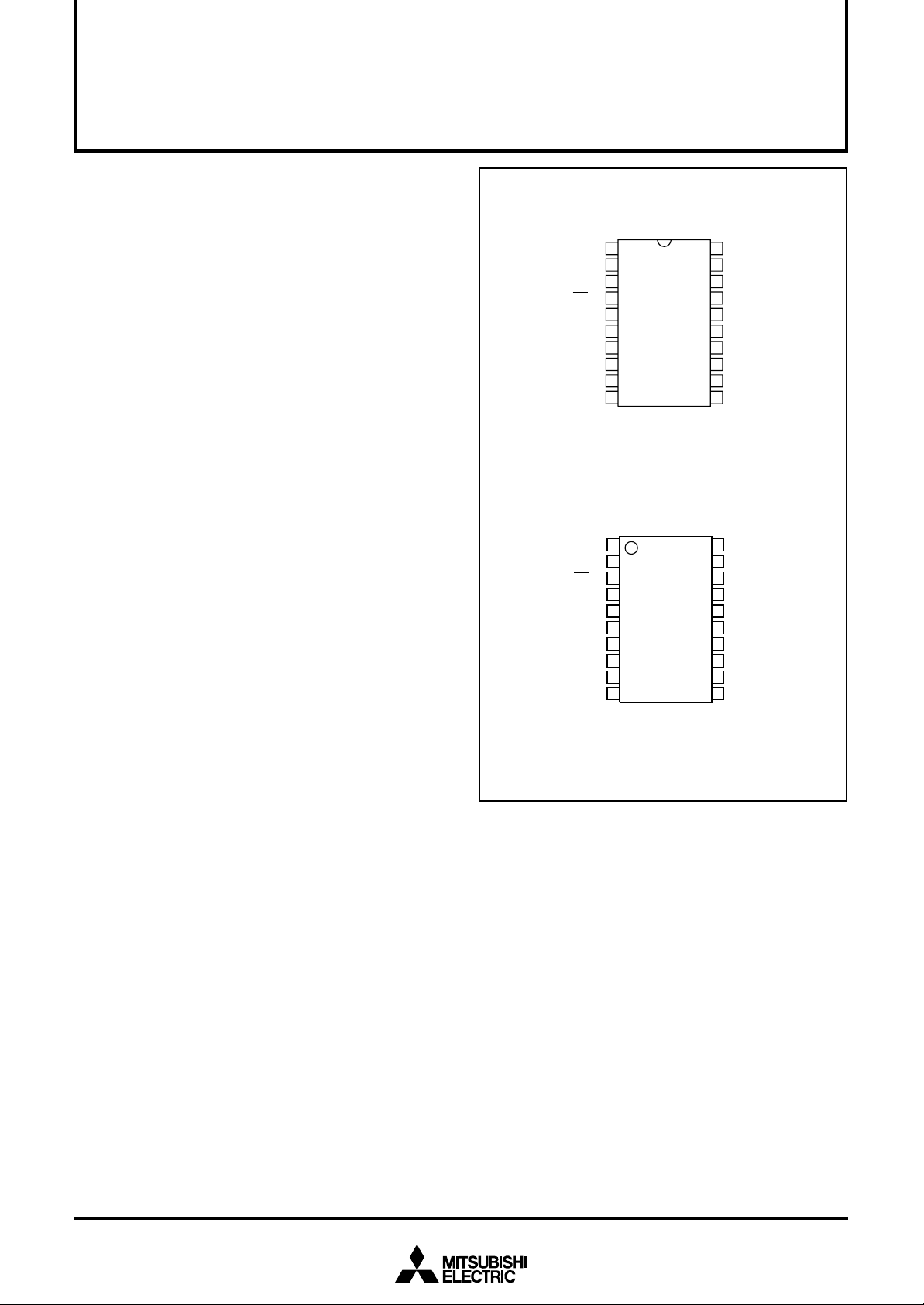
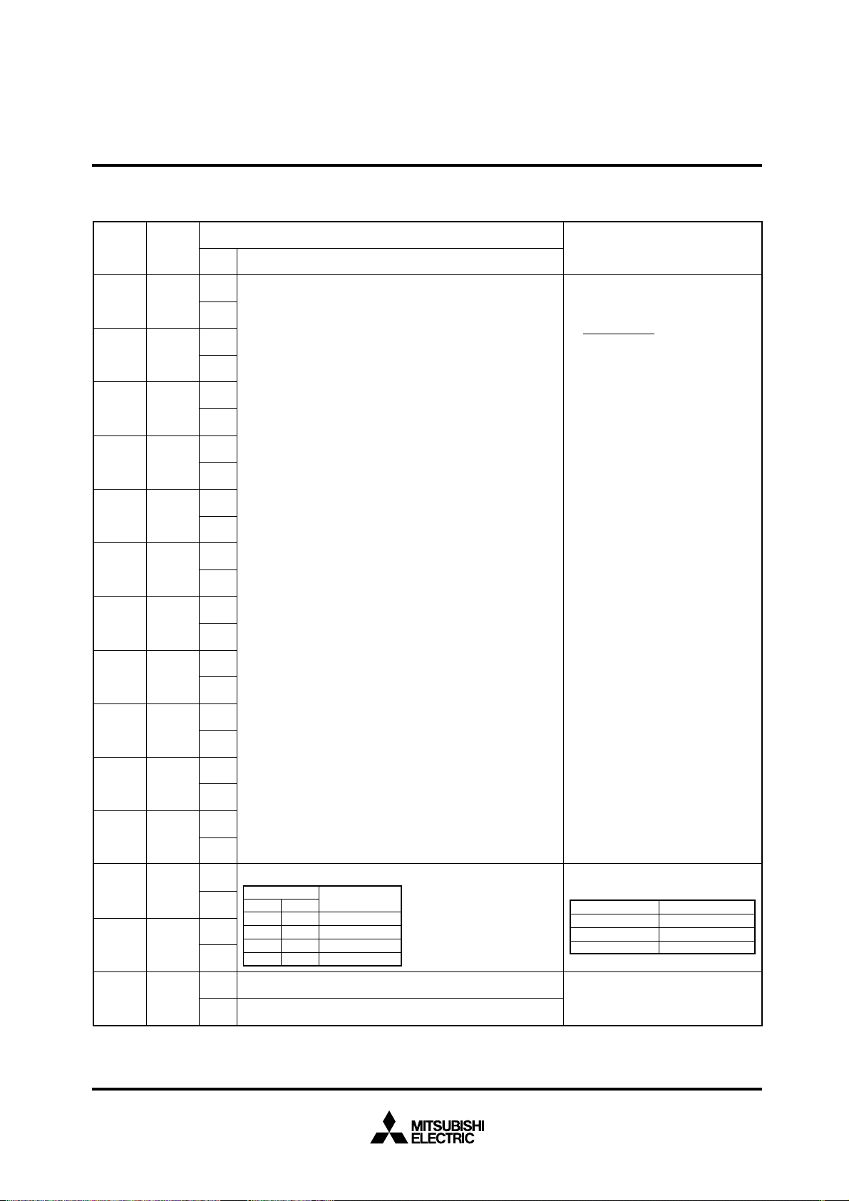
PIN CONFIGURATION (TOP VIEW)
←
VIR
AC
CS
SCK
SIN
TCK
DD1
V
P6
P7
1
2
→
3
→
4
→
5
→
6
→
7
8
←
9
←
10
M35045 - XXXSP
20
19
18
17
16
15
14
13
12
11
V
DD2
←
VERT
←
HOR
→
P5/B
→
P4
→
P3/G
→
P2
→
P1/R
→
P0/BLNK0
SS
V
CPOUT
Outline 20P4B
←
VIR
AC
CS
SCK
SIN
TCK
DD1
V
P6
P7
1
2
→
3
→
4
→
5
→
6
→
7
8
←
9
←
10
CPOUT
M35045 - XXXFP
20
19
18
17
16
15
14
13
12
11
V
DD2
←
VERT
←
HOR
→
P5/B
→
P4
→
P3/G
→
P2
→
P1/R
→
P0/BLNK0
V
SS
Outline 20P2Q-A
APPLICATION
Monitor
Rev.1.1
MITSUBISHI MICROCOMPUTERS
M35045-XXXSP/FP
SCREEN CHARACTER and PATTERN DISPLAY CONTROLLERS
PIN DESCRIPTION
Pin
Number
1
2
3
4
5
6
7
8
9
10
11
12
13
14
15
16
17
18
19
20
Symbol
CPOUT
VIR
__
AC
__
CS
SCK
SIN
TCK
DD1
V
P6
P7
VSS
P0/BLNK0
P1/R
P2
P3/G
P4
P5/B
HOR
VERT
V
DD2
Pin name
Phase difference
Frequency control
Auto-clear input
Chip select input
Serial clock input
Serial data input
Test clock
Power pin
Port P6 output
Port P7 output
Earthing pin
Port P0 output
Port P1 output
Port P2 output
Port P3 output
Port P4 output
Port P5 output
Horizontal synchro-
nization signal input
Vertical synchroni-
zation signal input
Power pin
Input/
Output
Output
–
Input
Input
Input
Input
Input
–
Output
Output
–
Output
Output
Output
Output
Output
Output
Input
Input
–
Function
Connect loop filter to this pin.
2.4kΩ∗1
0.1µF
1pin
4700pF
2
∗
2
∗
CPOUT
1 Use at 1% precision
∗
2 Use at 10% precision
∗
Connect to GND.
When “L”, this pin resets the internal IC circuit. Hysteresis input. Includes built-in pull-up
resistor.
This is the chip select pin, and when serial data transmission is being carried out, it goes
to “L”. Hysteresis input. Includes built-in pull-up resistor.
__
When CS pin is “L”, SIN serial data is taken in when SCK rises. Hysteresis input. Built-in
pull-up resistor is included.
This is the pin for serial input of data and addresses for the display control register and
the display data memory. Hysteresis input. Includes built-in pull-up resistor.
Input for test. Please connect to GND using circuit earthing pin.
Please connect to +5V with the power pin.
This is the output port. Port data is set by PTD6.
This is the output port. Port data is set by PTD7.
Please connect to GND using circuit earthing pin.
This pin can be toggled between port pin output and BLNK0 signal output.
This pin can be toggled between port pin output and R signal output.
This is the output port. Port data is set by PTD2.
This pin can be toggled between port pin output and G signal output.
This is the output port. Port data is set by PTD4.
This pin can be toggled between port pin output and B signal output.
This pin inputs the horizontal synchronization signal. Hysteresis input.
This pin inputs the vertical synchronization signal. Hysteresis input.
Please connect to +5V with the power pin.
2
MITSUBISHI MICROCOMPUTERS
M35045-XXXSP/FP
SCREEN CHARACTER and PATTERN DISPLAY CONTROLLERS
P0/BLNK0
16 P4
Port output
9P6
control circuit
10 P7
VERT
12
13 P1/R
15 P3/G
17 P5/B
14 P2
circuti
Polarity
19
switching
18
HOR
CPOUT
Polarity switching circuit
Clock oscillation
circuit for display
Input control circuit
H counter
switching circuit
Synchronous signal
Timing generator
circuit
Address control
circuit
Data control
detection circuit
Display location
register
Display control
Blinking circuit
control circuit
Reading address
Display RAM
circuit
Display control
Display character ROM Shift register
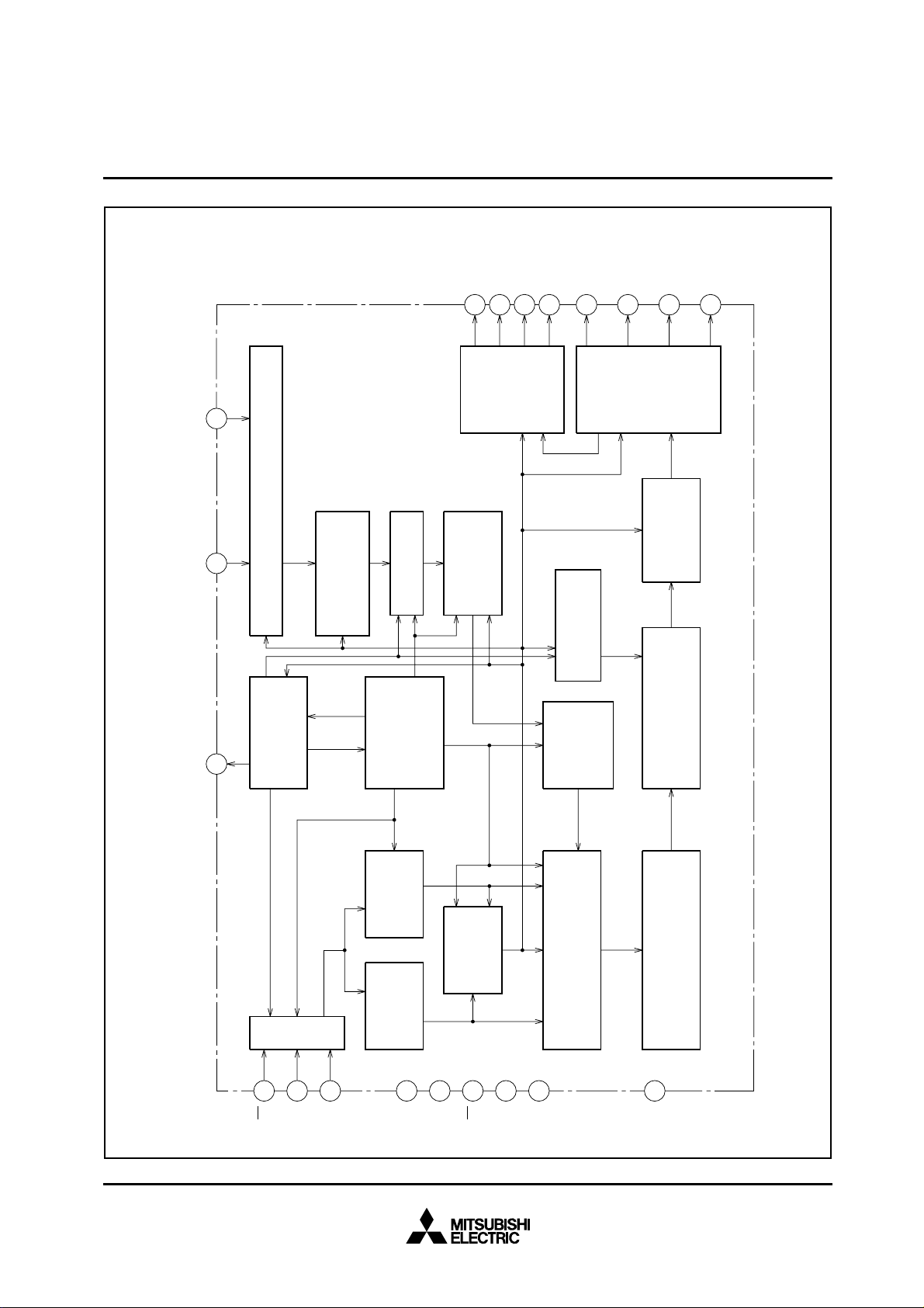
BLOCK DIAGRAM
415
CS
SCK
6
SIN
8
20
DD1VDD2
V
3
AC
2
11
SS
VIR
V
7
TCK
3
MITSUBISHI MICROCOMPUTERS
M35045-XXXSP/FP
SCREEN CHARACTER and PATTERN DISPLAY CONTROLLERS
MEMORY CONSTITUTION
Address 00016 to 11F16 are assigned to the display RAM, address
120
16 to 12816 are assigned to the display control registers. The in-
ternal circuit is reset and all display control registers (address 120
to 12816) are set to “0” and display RAM (address 00016 to 11F16)
are set to “FF16” when the AC pin level is “L”.
Memory constitution is shown in Figure 1.
DAF DAE DAD DAC DAB DAA DA9 DA8 DA7 DA6 DA5 DA4 DA3 DA2 DA1 DA0
000
………
11F16
12016
12116
12216
12316
12416
12516
0 BB BG BR BLINK B G R C7 C6 C5 C4 C3 C2 C1 C0
16
………
0 BB BG BR BLINK B G R C7 C6 C5 C4 C3 C2 C1 C0
0 0 DIVS2 DIVS1 DIVS0 DIV10 DIV9 DIV8 DIV7 DIV6 DIV5 DIV4 DIV3 DIV2 DIV1 DIV0
0 0 PTD7 PTD6 PTD5 PTD4 PTD3 PTD2 PTD1 PTD0 PTC5 PTC4 PTC3 PTC2 PTC1 PTC0
00
0 0 TEST3 TEST2 TEST1 TEST0 VP9 VP8 VP7 VP6 VP5 VP4 VP3 VP2 VP1 VP0
0 0 TEST5 TEST4 DSP11 DSP10 DSP9 DSP8 DSP7 DSP6 DSP5 DSP4 DSP3 DSP2 DSP1 DSP0
00
__
Background
coloring
SPACE2 SPACE1 SPACE0
Blinking
TEST9 HP9 HP8 HP7 HP6 HP5 HP4 HP3 HP2 HP1 HP0
VSZ1H1 VSZ1H0 VSZ1L1 VSZ1L0
Character color
V1SZ1 V1SZ0 LIN9 LIN8 LIN7 LIN6 LIN5 LIN4 LIN3 LIN2
SCREEN CONSTITUTION
The screen lines and rows are determined from each address of the
display RAM. The screen constitution is shown in Figure 2.
16
Character code
12616
12716
12816
00
0 0 HSZ21 HSZ20 HSZ11 HSZ10
00
Fig. 1 Memory constitution
Row
Line
123456789101112131415161718192021222324
1
0001600116002160031600416005160061600716008160091600A1600B1600C1600D1600E1600F1601016011160121601316014160151601616017
018160191601A1601B1601C1601D1601E1601F160201602116022160231602416025160261602716028160291602A1602B1602C1602D1602E1602F
2
0301603116032160331603416035160361603716038160391603A1603B1603C1603D1603E1603F1604016041160421604316044160451604616047
3
048160491604A1604B1604C1604D1604E1604F160501605116052160531605416055160561605716058160591605A1605B1605C1605D1605E1605F
4
0601606116062160631606416065160661606716068160691606A1606B1606C1606D1606E1606F1607016071160721607316074160751607616077
5
078160791607A1607B1607C1607D1607E1607F160801608116082160831608416085160861608716088160891608A1608B1608C1608D1608E1608F
6
0901609116092160931609416095160961609716098160991609A1609B1609C1609D1609E1609F160A0160A1160A2160A3160A4160A5160A6160A7
7
0A8160A9160AA160AB160AC160AD160AE160AF160B0160B1160B2160B3160B4160B5160B6160B7160B8160B9160BA160BB160BC160BD160BE160BF
8
0C0160C1160C2160C3160C4160C5160C6160C7160C8160C9160CA160CB160CC160CD160CE160CF160D0160D1160D2160D3160D4160D5160D6160D7
9
10
0D8160D9160DA160DB160DC160DD160DE160DF160E0160E1160E2160E3160E4160E5160E6160E7160E8160E9160EA160EB160EC160ED160EE160EF
11
0F0160F1160F2160F3160F4160F5160F6160F7160F8160F9160FA160FB160FC160FD160FE160FF1610016101161021610316104161051610616107
108161091610A1610B1610C1610D1610E1610F161101611116112161131611416115161161611716118161191611A1611B1611C1611D1611E1611F
12
* The hexadecimal numbers in the boxes show the display RAM address.
Fig. 2 Screen constitution
VSZ2H1 VSZ2H0 VSZ2L1 VSZ2L0 V18SZ1 V18SZ0
BETA14
TEST8 TEST7 TEST6 FB FG FR RB RG RR
BLINK2 BLINK1 BLINK0 DSPON
STOP
RAMERS
LIN17 LIN16 LIN15 LIN14 LIN13 LIN12 LIN11 LIN10
SYAD BLK1 BLK0 POLH POLV
VMASK__B/F BCOL
16
16
16
16
16
16
16
16
16
16
16
16
4
MITSUBISHI MICROCOMPUTERS
M35045-XXXSP/FP
SCREEN CHARACTER and PATTERN DISPLAY CONTROLLERS
REGISTERS DESCRIPTION
(1) Address 12016
RegisterDA
Status
0
0
DIV0
Set multiply value (frequency value) of horizontal synchronous frequency.
Function
Display frequency is computed as
shown below.
Remarks
1
FOSC = fH × N1
Contents
1
DIV1
1
0
2
DIV2
1
0
10
N1 = (DIVn × 2
Σ
n = 0
N1: frequency value
n
)
0
3
DIV3
1
F
OSC [MHz] : Display frequency
H [kHz] : Horizontal synchronous
f
signal frequency to HOR
pin.
N1 : Shown left
Set display frequency F
OSC to within
30MHz to 80MHz range.
When display frequency F
OSC, set fre-
quency value N2 in association with
DIVS0 and DIVS1.
0
4
DIV4
1
0
5
DIV5
1
0
6
DIV6
1
7
DIV7
1
0
0
8
DIV8
1
0
9
DIV9
1
0
A
DIV10
1
0
B
DIVS0
C
DIVS1
D
DIVS2
Set frequency value N2
1
0
1
0
1
DIVS Frequency
1
0
0
1
1
It should be fixed to “0”.
Can not be used.
0
0
1
0
1
value N2
Division into 2
Division into 3
Division into 4
Do not set
__
Note: The mark ⁄ around the status value means the reset status by the “L” level is input to AC pin.
Set frequency value N2 in association
with display frequency range.
Display frequency
55 ~ 80
40 ~ 55
30 ~ 40
Frequency value N2
Division into 2
Division into 3
Division into 4
5
MITSUBISHI MICROCOMPUTERS
M35045-XXXSP/FP
SCREEN CHARACTER and PATTERN DISPLAY CONTROLLERS
(2) Address 121
RegisterDA
0
PTC0
1
PTC1
2
PTC2
3
PTC3
4
PTC4
5
PTC5
6
16
PTD0
Contents
Status
0
P0 output (port P0). Port data is set by PTD0.
1
BLNK0 output. Polarity is set by PTD0.
0
P1 output (port P1). Port data is set by PTD1.
1
R signal output. Polarity is set by PTD1.
0
P2 output (port P2). Port data is set by PTD2.
1
Do not set.
0
P3 output (port P3). Port data is set by PTD3.
1
G signal output. Polarity is set by PTD3.
0
P4 output (port P4). Port data is set by PTD4.
1
Do not set.
0
P5 output (port P5). Port data is set by PTD5.
1
B signal output. Polarity is set by PTD5.
0
“L” output (P0 output) or negative polarity output (BLNK0 output).
1
“H” output (P0 output) or positive polarity output (BLNK0 output).
Function
Remarks
BLNK0 outputs blanking signal.
Blanking status is determined by BLK0,
BLK1, and DSP0 to DSP11 settings.
P0 pin data control.
0
7
PTD1
8
PTD2
9
PTD3
A
PTD4
B
PTD5
C
PTD6
D
PTD7
“L” output (P1 output) or negative polarity output (R signal output).
1
“H” output (P1 output) or positive polarity output (R signal output).
0
“L” output (P2 output).
1
“H” output (P2 output).
0
“L” output (P3 output) or negative polarity output (G signal output).
1
“H” output (P3 output) or positive polarity output (G signal output).
0
“L” output (P2 output).
1
“H” output (P2 output).
0
“L” output (P5 output) or negative polarity output (B signal output).
1
“H” output (P5 output) or positive polarity output (B signal output).
0
“L” output (P6 output).
1
“H” output (P6 output).
0
“L” output (P7 output).
1
“H” output (P7 output).
P1 pin data control.
P2 pin exclusive port output state control.
P3 pin data control.
P4 pin exclusive port output state control.
P5 pin data control.
P6 pin exclusive port output state control.
P7 pin exclusive port output state control.
6
MITSUBISHI MICROCOMPUTERS
M35045-XXXSP/FP
SCREEN CHARACTER and PATTERN DISPLAY CONTROLLERS
(3) Address 12216
Register
Status
0
0
1
2
3
HP0
(LSB)
HP1
HP2
HP3
If HS is the horizontal display start location,
9
1
HS = T × (
0
1
HSZ11
HSZ21
0
1
1000 settings are possible.
0
n
2
HPn + N).
Σ
n = 0
T: The cycle of display frequency
HSZ10
0
0
1
1
HSZ20
Function
Horizontal display start location is
specified using the 10 bits from HP9
to HP0.
Note: HP9 to 0 = (0000000000
(0000010111
N
0
1
0
1
6
7
8
9
RemarksDA
2) and
2) setting is forbidden
1
0
Contents
4
HP4
1
0
5
HP5
1
0
6
HP6
1
7
HP7
1
0
0
8
HP8
1
9
A
B
C
D
HP9
(MSB)
TEST9
SPACE0
SPACE1
SPACE2
0
1
0
It should be fixed to “0”.
1
Can not be used.
0
1
0
1
0
1
SPACE
2
0
0
0
0
1
1
1
1
0
1
0
0
1
0
0
1
1
1
0
0
1
0
0
1
1
1
Í represents one line worth of spaces.
Number of Lines and Space
(Í represents space)
12
1 Í 10 Í 1
2 Í 8 Í 2
3 Í 6 Í 3
4 Í 4 Í 4
5 Í 2 Í 5
6 Í 6
6 Í Í 6
Leave one line worth of space in the vertical direction.
For example, 6 Í 6 indicates two sets
of 6 lines with a line of spaces between
lines 6 and 7.
A line is 18 × N horizontal scan lines.
N is determined by the character size in
the vertical direction as follows:
×1 N = 1 ×2 N = 2
×3 N = 3 ×4 N = 4
7
MITSUBISHI MICROCOMPUTERS
M35045-XXXSP/FP
SCREEN CHARACTER and PATTERN DISPLAY CONTROLLERS
(4) Address 12316
Contents
RegisterDA
Status
0
0
1
VP0
(LSB)
VP1
If VS is the vertical display start location,
9
1
VS = H × (
0
H: Cycle with the horizontal synchronizing pulse
2
Σ
n = 0
n
VPn).
1023 settings are possible.
Function
The vertical start location is specified
using the 10 bits from VP9 to VP0.
VP9 to VP0 = (0000000000
forbidden.
Note 1: In case of B/F register is “0”.
Remarks
2) setting is
_
1
0
HOR
2
VP2
1
VP
0
3
4
VP3
VP4
0
VERT
HP
Character
displaying area
1
1
0
5
VP5
1
0
6
VP6
1
7
VP7
1
0
0
8
VP8
1
9
A
B
C
D
VP9
(MSB)
TEST0
TEST1
TEST2
TEST3
0
1
0
It should be fixed to “0”.
1
Can not be used.
0
It should be fixed to “0”.
1
Can not be used.
0
It should be fixed to “0”.
1
Can not be used.
0
It should be fixed to “0”.
1
Can not be used.
8
MITSUBISHI MICROCOMPUTERS
M35045-XXXSP/FP
SCREEN CHARACTER and PATTERN DISPLAY CONTROLLERS
(5) Address 124
RegisterDA
0
DSP0
1
DSP1
2
DSP2
3
DSP3
4
DSP4
5
DSP5
6
DSP6
16
Contents
Status
0
Blanking is in the display mode specified by BLK0 and BLK1. (Note)
1
Blanking is in the display mode specified by except BLK0 and BLK1.
0
Blanking is in the display mode specified by BLK0 and BLK1. (Note)
1
Blanking is in the display mode specified by except BLK0 and BLK1.
0
Blanking is in the display mode specified by BLK0 and BLK1. (Note)
1
Blanking is in the display mode specified by except BLK0 and BLK1.
0
Blanking is in the display mode specified by BLK0 and BLK1. (Note)
1
Blanking is in the display mode specified by except BLK0 and BLK1.
0
Blanking is in the display mode specified by BLK0 and BLK1. (Note)
1
Blanking is in the display mode specified by except BLK0 and BLK1.
0
Blanking is in the display mode specified by BLK0 and BLK1. (Note)
1
Blanking is in the display mode specified by except BLK0 and BLK1.
0
Blanking is in the display mode specified by BLK0 and BLK1. (Note)
1
Blanking is in the display mode specified by except BLK0 and BLK1.
Function
Sets the display mode of line 1.
Sets the display mode of line 2.
Sets the display mode of line 3.
Sets the display mode of line 4.
Sets the display mode of line 5.
Sets the display mode of line 6.
Sets the display mode of line 7.
Remarks
7
DSP7
8
DSP8
9
DSP9
A
DSP10
B
DSP11
C
TEST4
D
TEST5
Note: Refer to DISPLAY FORM1.
0
1
0
1
0
1
0
1
0
1
0
1
0
1
Blanking is in the display mode specified by BLK0 and BLK1. (Note)
Blanking is in the display mode specified by except BLK0 and BLK1.
Blanking is in the display mode specified by BLK0 and BLK1. (Note)
Blanking is in the display mode specified by except BLK0 and BLK1.
Blanking is in the display mode specified by BLK0 and BLK1. (Note)
Blanking is in the display mode specified by except BLK0 and BLK1.
Blanking is in the display mode specified by BLK0 and BLK1.
Blanking is in the display mode specified by except BLK0 and BLK1.
Blanking is in the display mode specified by BLK0 and BLK1.
Blanking is in the display mode specified by except BLK0 and BLK1.
It should be fixed to “0”.
Can not be used.
It should be fixed to “0”.
Can not be used.
Sets the display mode of line 8.
Sets the display mode of line 9.
Sets the display mode of line 10.
Sets the display mode of line 11.
Sets the display mode of line 12.
9

MITSUBISHI MICROCOMPUTERS
M35045-XXXSP/FP
SCREEN CHARACTER and PATTERN DISPLAY CONTROLLERS
(6) Address 125
RegisterDA
0
1
2
3
4
5
6
7
8
V1SZ0
9
V1SZ1
16
LIN2
LIN3
LIN4
LIN5
LIN6
LIN7
LIN8
LIN9
Contents
Status
The first line is set by VSZ1L0 and VSZ1L1.
0
The second to 12th lines are set by VSZ2L0 and VSZ2L1.
The first line is set by VSZ1H0 and VSZ1H1.
1
The second to 12th lines are set by VSZ2H0 and VSZ2H1.
The first line is set by VSZ1L0 and VSZ1L1.
0
The second to 12th lines are set by VSZ2L0 and VSZ2L1.
The first line is set by VSZ1H0 and VSZ1H1.
1
The second to 12th lines are set by VSZ2H0 and VSZ2H1.
The first line is set by VSZ1L0 and VSZ1L1.
0
The second to 12th lines are set by VSZ2L0 and VSZ2L1.
The first line is set by VSZ1H0 and VSZ1H1.
1
The second to 12th lines are set by VSZ2H0 and VSZ2H1.
The first line is set by VSZ1L0 and VSZ1L1.
0
The second to 12th lines are set by VSZ2L0 and VSZ2L1.
The first line is set by VSZ1H0 and VSZ1H1.
1
The second to 12th lines are set by VSZ2H0 and VSZ2H1.
The first line is set by VSZ1L0 and VSZ1L1.
0
The second to 12th lines are set by VSZ2L0 and VSZ2L1.
The first line is set by VSZ1H0 and VSZ1H1.
1
The second to 12th lines are set by VSZ2H0 and VSZ2H1.
The first line is set by VSZ1L0 and VSZ1L1.
0
The second to 12th lines are set by VSZ2L0 and VSZ2L1.
The first line is set by VSZ1H0 and VSZ1H1.
1
The second to 12th lines are set by VSZ2H0 and VSZ2H1.
The first line is set by VSZ1L0 and VSZ1L1.
0
The second to 12th lines are set by VSZ2L0 and VSZ2L1.
The first line is set by VSZ1H0 and VSZ1H1.
1
The second to 12th lines are set by VSZ2H0 and VSZ2H1.
The first line is set by VSZ1L0 and VSZ1L1.
0
The second to 12th lines are set by VSZ2L0 and VSZ2L1.
The first line is set by VSZ1H0 and VSZ1H1.
1
The second to 12th lines are set by VSZ2H0 and VSZ2H1.
0
H: Cycle with the horizontal synchronizing pulse
V1SZ0
0
1
0
1
Vertical direction size
0
V1SZ1
1
1
0
0
1
1
Function
1H/dot
2H/dot
3H/dot
4H/dot
Remarks
Character size setting in the vertical
direction for the 2nd line.
Character size setting in the vertical
direction for the 3rd line.
Character size setting in the vertical
direction for the 4th line.
Character size setting in the vertical
direction for the 5th line.
Character size setting in the vertical
direction for the 6th line.
Character size setting in the vertical
direction for the 7th line.
Character size setting in the vertical
direction for the 8th line.
Character size setting in the vertical
direction for the 9th line.
Character size setting in the vertical
direction for the 1st line.
(display monitor 1 ~ 12 line)
10
0
VSZ1L0
B
VSZ1L1
C
VSZ1H0
D
VSZ1H1
VSZ1L1
1
0
1
0
1
0
1
0
0
1
1
H: Cycle with the horizontal synchronizing pulse
VSZ1H1
0
0
1
1
VSZ1L0
0
1
0
1
VSZ1H0
0
1
0
1
Vertical direction size
1H/dot
2H/dot
3H/dot
4H/dot
Vertical direction size
1H/dot
2H/dot
3H/dot
4H/dot
A
H: Cycle with the horizontal synchronizing pulse
Character size setting in the vertical
direction (display monitor 1 line) at “0”
state in register LIN2 ~ LIN17.
Character size setting in the vertical
direction (display monitor 1 line) at “1”
state in register LIN2 ~ LIN17.

MITSUBISHI MICROCOMPUTERS
M35045-XXXSP/FP
SCREEN CHARACTER and PATTERN DISPLAY CONTROLLERS
(7) Address 126
RegisterDA
0
LIN10
1
LIN11
2
LIN12
3
LIN13
4
LIN14
5
LIN15
6
LIN16
7
LIN17
8
V18SZ0
9
V18SZ1
16
Contents
Remarks
Status
The first line is set by VSZ1L0 and VSZ1L1.
0
The second to 12th lines are set by VSZ2L0 and VSZ2L1.
The first line is set by VSZ1H0 and VSZ1H1.
1
The second to 12th lines are set by VSZ2H0 and VSZ2H1.
The first line is set by VSZ1L0 and VSZ1L1.
0
The second to 12th lines are set by VSZ2L0 and VSZ2L1.
The first line is set by VSZ1H0 and VSZ1H1.
1
The second to 12th lines are set by VSZ2H0 and VSZ2H1.
The first line is set by VSZ1L0 and VSZ1L1.
0
The second to 12th lines are set by VSZ2L0 and VSZ2L1.
The first line is set by VSZ1H0 and VSZ1H1.
1
The second to 12th lines are set by VSZ2H0 and VSZ2H1.
The first line is set by VSZ1L0 and VSZ1L1.
0
The second to 12th lines are set by VSZ2L0 and VSZ2L1.
The first line is set by VSZ1H0 and VSZ1H1.
1
The second to 12th lines are set by VSZ2H0 and VSZ2H1.
The first line is set by VSZ1L0 and VSZ1L1.
0
The second to 12th lines are set by VSZ2L0 and VSZ2L1.
The first line is set by VSZ1H0 and VSZ1H1.
1
The second to 12th lines are set by VSZ2H0 and VSZ2H1.
The first line is set by VSZ1L0 and VSZ1L1.
0
The second to 12th lines are set by VSZ2L0 and VSZ2L1.
The first line is set by VSZ1H0 and VSZ1H1.
1
The second to 12th lines are set by VSZ2H0 and VSZ2H1.
The first line is set by VSZ1L0 and VSZ1L1.
0
The second to 12th lines are set by VSZ2L0 and VSZ2L1.
The first line is set by VSZ1H0 and VSZ1H1.
1
The second to 12th lines are set by VSZ2H0 and VSZ2H1.
The first line is set by VSZ1L0 and VSZ1L1.
0
The second to 12th lines are set by VSZ2L0 and VSZ2L1.
The first line is set by VSZ1H0 and VSZ1H1.
1
The second to 12th lines are set by VSZ2H0 and VSZ2H1.
0
H: Cycle with the horizontal synchronizing pulse
V18SZ0
0
1
0
1
Vertical direction size
0
V18SZ1
1
1
0
0
1
1
1H/dot
2H/dot
3H/dot
4H/dot
Function
Character size setting in the vertical
direction for the 10th line.
Character size setting in the vertical
direction for the 11th line.
Character size setting in the vertical
direction for the 12th line.
Character size setting in the vertical
direction for the 13th line.
Character size setting in the vertical
direction for the 14th line.
Character size setting in the vertical
direction for the 15th line.
Character size setting in the vertical
direction for the 16th line.
Character size setting in the vertical
direction for the 17th line.
Character size setting in the vertical
direction for the 18th line.
(display monitor 1 ~ 12 line)
0
VSZ2L0
B
VSZ2L1
C
VSZ2H0
D
VSZ2H1
VSZ2L1
1
0
1
0
1
0
1
0
0
1
1
H: Cycle with the horizontal synchronizing pulse
VSZ2H1
0
0
1
1
VSZ2L0
0
1
0
1
VSZ2H0
0
1
0
1
Vertical direction size
1H/dot
2H/dot
3H/dot
4H/dot
Vertical direction size
1H/dot
2H/dot
3H/dot
4H/dot
A
H: Cycle with the horizontal synchronizing pulse
Character size setting in the vertical
direction (display monitor for 2 ~ 12 line)
at “0” state in register LIN2 ~ LIN17.
Character size setting in the vertical
direction (display monitor for 2 ~ 12 line)
at “1” state in register LIN2 ~ LIN17.
11

MITSUBISHI MICROCOMPUTERS
M35045-XXXSP/FP
SCREEN CHARACTER and PATTERN DISPLAY CONTROLLERS
(8) Address 127
RegisterDA
0
1
2
3
4
5
6
TEST6
RR
RG
RB
FR
FG
FB
16
Contents
Remarks
Status
0
1
0
1
0
RB
0
0
0
0
1
1
1
1
RG
0
0
1
1
0
0
1
1
RR
0
1
0
1
0
1
0
1
Function
Color
Black
Red
Green
Yellow
Blue
Magenta
Cyan
White
Sets the color of all blankings.
1
0
0
0
BB
1
1
0
0
0
0
1
1
1
1
BG
0
BR
0
1
1
0
0
1
1
Color
Black
0
1
0
1
0
1
0
1
Red
Green
Yellow
Blue
Magenta
Cyan
White
Sets the blanking color of the Border
size, or the shadow size.
1
0
It should be fixed to “0”.
1
Can not be used.
0
7
TEST7
8
TEST8
9
BETA14
A
HSZ10
B
HSZ11
C
HSZ20
D
HSZ21
It should be fixed to “0”.
1
Can not be used.
0
It should be fixed to “0”.
1
Can not be used.
0
Matrix-outline display (12 × 18 dot)
1
Matrix-outline display (14 × 18 dot)
0
T: Display frequency cycle
HSZ10
0
1
0
1
HSZ20
0
1
0
1
Vertical direction size
Vertical direction size
HSZ11
1
0
1
0
1
0
1
0
0
1
1
T: Display frequency cycle
VSZ21
0
0
1
1
Set this register to the character font
set by display RAM BR, BG and BB.
Character size setting in the vertical
direction for the first line.
1T/dot
2T/dot
3T/dot
4T/dot
Character size setting in the vertical
direction for the 2nd line to 12th line.
1T/dot
2T/dot
3T/dot
4T/dot
12

MITSUBISHI MICROCOMPUTERS
M35045-XXXSP/FP
SCREEN CHARACTER and PATTERN DISPLAY CONTROLLERS
(9) Address 128
RegisterDA
0
BCOL
1
VMASK
2
POLV
3
POLH
4
BLK0
5
BLK1
6
16
B/F
Contents
Remarks
Status
0
Blanking of BLK0, BLK1
1
All raster blanking
0
__
Synchronize with the leading edge of horizontal synchronization.
1
Synchronize with the trailing edge of horizontal synchronization.
0
Do not mask by VERT input signal
Function
Sets all raster blanking
Synchronize with the front porch or
back porch of the horizontal
synchronazation signal.
This register has or do not have mask
at phase comparison operating.
1
Mask by VERT input signal
0
VERT pin polarity is negative electrode
1
VERT pin polarity is positive electrode
0
HOR pin polarity is negative electrode
1
HOR pin polarity is positive electrode
0
1
0
1
BLK
1
0
0
1
1
0
0
Matrix-outline size
1
Character size
0
Border size
1
Matrix-outline size
Blanking mode
Set VERT pin polarity.
Set HOR pin polarity.
Set blanking mode. (Note 1)
An example of blanking mode at
BCOL = “0”, DSPn = “0” (n = 0 ~ 11)
shown left.
0
7
8
9
A
SYAD
RAMERS
STOP
DSPON
Border display of character
1
Shadow display of character
0
RAM not erased
1
RAM erased
0
Oscillation of clock for display
1
Stop the oscillation of clock for display
0
Display OFF
1
Display ON
0
BLINK0
B
1
0
BLINK1
C
1
0
BLINK2
D
Divided into 64 of vertical synchronous signal
1
Divided into 32 of vertical synchronous signal
Notes 1: Refer to DISPLAY FORM 1
2: Refer to DISPLAY FORM 3
BLINK
1
0
0
1
1
(Note 2)
There is no need to reset because
there is no register for this bit.
R, G, B and BLNK0 output can be
altered.
Display can be altered.
Blinking duty ratio can be altered.
0
0
1
0
1
Duty
Blinking OFF
25%
50%
75%
Blinking frequency can be altered.
13

MITSUBISHI MICROCOMPUTERS
M35045-XXXSP/FP
SCREEN CHARACTER and PATTERN DISPLAY CONTROLLERS
DISPLAY FORM1
Table 1 shows display form of blanking.
Table 1. Display mode
BCOL
0
1
(Note 1)
Standard blanking
BLK0BLK1
0
0
1
1
0
0
1
1
When the all of registers
DSPn (Note 2) are set to “0”
Matrix-outline and border display.
color set: FR, FG, FB
0
or display RAM (Note 4)
Character
1
Border display
color set: display RAM
0
(Note 3)
Matrix-outline display
color set: display RAM
1
(Note 3)
Matrix-outline and border display.
color set: FR, FG, FB
0
or display RAM (Note 4)
Character
1
Border display
color set: display RAM
0
(Note 3)
Matrix-outline display
color set: display RAM
1
(Note 3)
Notes 1: Color setting of raster area is set by register RR, RG and RB.
2: DSPn (n = 0 ~ 11)
3: Set by BR, BG and BB of
display RAM.
4: Set border by register FR, FG and FB. Set matrix-outline by BR, BG and BB of
When some of registers DSPi are set to “1”
DSPn = 0
Matrix-outline and border display.
color set: FR, FG, FB
or display RAM (Note 4)
Character
Border display
color set: display RAM
(Note 3)
Matrix-outline display
color set: display RAM
(Note 3)
Matrix-outline and border display.
color set: FR, FG, FB
or display RAM (Note 4)
Character
Border display
color set: display RAM
(Note 3)
Matrix-outline display
color set: display RAM
(Note 3)
Matrix-outline display
color set: display RAM
(Note 3)
Border display
color set: display RAM
(Note 3)
Matrix-outline display
color set: display RAM
(Note 3)
Character
Matrix-outline display
color set: display RAM
(Note 3)
Border display
color set: display RAM
(Note 3)
Matrix-outline display
color set: display RAM
(Note 3)
Character
DSPn = 1
display RAM.
BLNK0 output
DSPn = “0” line
DSPn = “1” line
DSPn = “0” line→Character size
DSPn = “1” line→Border size
DSPn = “0” line→Border size
DSPn = “1” line→
DSPn = “0” line→
DSPn = “1” line→Character size
All blanking size
Matrix-outline size
Matrix-outline size
Matrix-outline size
14

MITSUBISHI MICROCOMPUTERS
M35045-XXXSP/FP
SCREEN CHARACTER and PATTERN DISPLAY CONTROLLERS
Display form 2
M35045-XXXSP has the following four display forms.
(1) Character size
: Blanking same as the character size.
(2) Border size
: Blanking the background as a size from character.
(3) Matrix-outline size
: Blanking the background 12 × 18 dot.
When set register BETA14 to “1”, setting of blanking the
background 14 × 18 dot is possible.
(4) All blanking size
: When set register BCOL to “1”, all raster area is blanking.
〈 Register BCOL = “0” 〉
Scanning
Set character color by display
1
∗
(address 0 to 11F16)
RAM
R,G or B output
BLNK0 output
(1) Character display
(character size)
〈 Register BCOL = “1” 〉
Scanning
Set character color by display
1
∗
RAM
(address 0 to 11F16)
12dots 12dots 12dots 12dots
Set border color by
display RAM
2
∗
12dots 12dots 12dots 12dots
Set raster area
color by register
RR,RG and RB
1
∗
(2) Border display
(border size)
Set matrix - outline
color by display
RAM
Set matrix - outline
color by display
RAM
3
∗
(3) Matrix - outline
display
(matrix-outline size)
3
∗
Set border
color by register
FR,FG and FB
Set matrix - outline
color by RAM
for display
(4) Matrix - outline
and border display
(matrix-outline size)
Set border
color by register
FR,FG and FB
3
∗
R,G or B output
BLNK0 output
Fig. 3 Display form
“H” level
GND level
(1) Character display
(all blanking size)
Set border color by
display RAM
2
∗
(2) Border display
(all blanking size)
1 Red,Blue,Yellow,Green,Magenta,Cyan, White and Black are set possible.
∗
2 ( ) is blanking mode.
∗
3 All matrix - outline horizontal direction size is able to set to 14dots by register BETA14
∗
(BLNK0 output by 14dots).
1
∗
(3) Matrix - outline
display
(all blanking size)
Set matrix - outline
color by display
RAM
3
∗
(4) Matrix - outline
and border display
(all blanking size)
15

MITSUBISHI MICROCOMPUTERS
M35045-XXXSP/FP
SCREEN CHARACTER and PATTERN DISPLAY CONTROLLERS
Display form 3
When border display mode, if set SYAD = “0” to “1”, it change to
shadow display mode.
Border and shadow display are shown below.
Border display Shadow display
Fig. 4 Border and shadow display
Set shadow display color by display RAM or register FR, FG and FB.
16

MITSUBISHI MICROCOMPUTERS
M35045-XXXSP/FP
SCREEN CHARACTER and PATTERN DISPLAY CONTROLLERS
DATA INPUT EXAMPLE
Data of display RAM and display control registers can be set by the
serial input function. Example of data setting is shown in Figure 5.
Example of data setting by the serial input function (M35045-XXXSP/FP)
1
address 12016
2
data 12016
3
data 12116
4
data 12216
5
data 12316
6
data 12416
7
data 12516
8
data 12616
9
data 12716
10
data 12816
11
data 00016
12
………
297
…………
DAF DAE DAD DAC DAB DAA DA9 DA8 DA7 DA6 DA5 DA4 DA3 DA2 DA1 DA0
200 msec hold
0000000100100000
000
00
0 0 0 0 0 0 HP9 HP8 HP7 HP6 HP5 HP4 HP3 HP2 HP1 HP0
0 0 0 0 0 0 VP9 VP8 VP7 VP6 VP5 VP4 VP3 VP2 VP1 VP0
0000000000000000
0000000000000000
0000000000000000
0000000000000000
00000001011
0BBBGBR
…………
background
DIVS1 DIVS0 DIV10
PTD7PTD61PTD41PTD2
BLINK
Character
color
Blinking
DIV9 DIV8 DIV7 DIV6 DIV5 DIV4 DIV3 DIV2 DIV1 DIV0
200 msec hold
B G R C7C6C5C4C3C2C1C0
Character
color
11101011
POLH POLV
Character code
000
Addition
System set-up
Address set
Setting frequency
dividing value (Note 1)
Output setting
Horizontal display
location setting
Vertical display
location setting
Display form setting
Character size setting
Character size setting
Color,
character size setting
Display OFF,
display form (Note 2)
Character setting
298
data 11F16
299
address 12816
300
data 12816
Notes 1: Input horizontal synchronous signal to HOR pin.
2: Matrix-outline display in this data.
Fig. 5 Example of data setting by the serial input function
0BBBGBR
0000000100101000
00000100011
BLINK
B G R C7C6C5C4C3C2C1C0
POLH POLV
000
Address setting
Display ON, display
form (Note 2)
17

MITSUBISHI MICROCOMPUTERS
M35045-XXXSP/FP
SCREEN CHARACTER and PATTERN DISPLAY CONTROLLERS
SERIAL DATA INPUT TIMING
(1) Serial data should be input with the LSB first.
(2) The address consists of 16 bits.
(3) The data consists of 16 bits.
(4)
The 16 bits in the SCK after the CS signal has fallen are the
address, and for succeeding input data, the address is
incremented every 16 bits.
CS
__
SCK
SIN
LSB MSB LSB MSB LSB MSB
Fig. 6 Serial input timing
Address(16 bits) Data(16 bits)
N
Data(16 bits)
N + 1
N = 1,2,3
………
18

MITSUBISHI MICROCOMPUTERS
M35045-XXXSP/FP
SCREEN CHARACTER and PATTERN DISPLAY CONTROLLERS
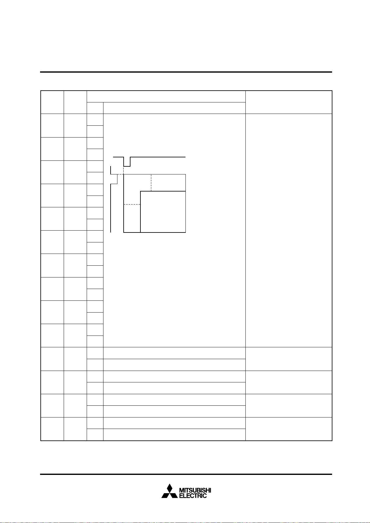
CHARACTER FONT
Images are composed on a 12 × 18 dot matrix, and characters can
be linked vertically and horizontally with other characters to allow the
display the continuous symbols.
12 dots
18 dots
When the character extends
to the top line of the matrix,
no border is left at the top.
When the character extends
to the bottom(18th) line of
the matrix, no border is left
at the bottom.
Note : Hatching represents
border.
Fig. 7 Example for displaying a continuous pattern after combining characters in the horizontal or vertical direction
Character code FF
16 is fixed as a blank without background.
Therefore, you cannot register a character font in this code.
19

MITSUBISHI MICROCOMPUTERS
M35045-XXXSP/FP
SCREEN CHARACTER and PATTERN DISPLAY CONTROLLERS
TIMING REQUIREMENTS (Ta = –20°C to + 85°C, VDD = 5±0.25V, unless otherwise noted)
Symbol
w(SCK)
t
__
tsu(CS)
__
th(CS)
tsu(SIN)
th(SIN)
tword
SCK width
__
CS setup time
__
CS hold time
SIN setup time
SIN hold time
1 word writing time
Parameter
Min.
200
200
2
200
200
10
Limits
Typ.
—
—
—
—
—
—
Max.
Unit
—
—
—
—
—
—
ns
ns
µs
ns
ns
µs
tw(CS)
1ms(min.)
Remarks
See Figure 8
CS
SCK
SIN
CS
SCK
tsu(CS) tw(SCK) tw(SCK)
tsu(SIN) th(SIN)
tword
more than 2 µs
1 2 12 13 14 15 16
…
th(CS)
…
1 1213141516
Fig. 8 Serial input timing requirements
20

MITSUBISHI MICROCOMPUTERS
M35045-XXXSP/FP
SCREEN CHARACTER and PATTERN DISPLAY CONTROLLERS
EXAMPLE OF THE M35045-XXXSP/FP CLOCK PERIPHERAL CIRCUIT
Horizontal synchronous signal (5V)
Synchronous signal
generator
Vertical synchronous signal (5V)
+ 5V
2.4kΩ(Note1)
0.1mF(Note2)
Microcomputer
Note 1 : Use this 1% precision element.
Note 2 : Use this 10% precision element.
4700pF(Note2)
+
1µF
+ 5V
1
CPOUT
2
VIR
–
3
AC
4
CS
5
SCK
6
SIN
7
TCK
8
V
9
P6
10
P7
M35045 - XXXSP
DD1
P0/BLNK0
100µF
+
–
1µF
0.01µF
V
DD2
VERT
HOR
P5/B
P4
P3/G
P2
P1/R
V
20
19
18
17
16
15
14
13
12
11
SS
100µF
+
–
1µF
0.01µF
B
G
R
BLNK0
Mixing
video pre - amp
Fig. 9 Example of the M35045-XXXSP peripheral circuit (M35045-XXXFP peripheral circuit is same as that of M35045-XXXSP)
Note for waveform timing of the horizontal signals to the HOR pin.
Set horizontal synchronous signal edge∗ waveform timing to under
5ns and input to HOR pin.
Set only the side which set by B/F register waveform timing under
5ns and input to HOR pin.
∗
: Set front porch edge or back porch edge by B/F register.
_
_
Horizontal synchronous signal input
90%
10%
tf
tr
21

MITSUBISHI MICROCOMPUTERS
M35045-XXXSP/FP
SCREEN CHARACTER and PATTERN DISPLAY CONTROLLERS
ABSOLUTE MAXIMUM RATINGS
Symbol
DD
V
VI
VO
Pd
Topr
Tstg
Supply voltage
Input voltage
Output voltage
Power dissipation
Operating temperature
Storage temperature
RECOMMENDED OPERATING CONDITIONS (VDD = 5V, Ta = –20 to +85°C, unless otherwise noted)
Symbol
VDD
VIH
VIL
FOSC
Supply voltage
“H” level input voltage SIN, SCK, CS, AC HOR, VERT
“L” level input voltage SIN, SCK, CS, AC HOR, VERT
Oscillating frequency for display
Parameter
Parameter
__ __
__ __
Conditions
With respect to V
Ta = 25°C
Min.
4.75
DD
0.8V
0
30.0
SS.
Limits
Typ.
5.0
DD
V
0
—
Max.
5.25
DD
V
0.2VDD
80.0
Ratings
–0.3 to +6.0
SS –0.3 < VI < VDD +0.3
V
SS < VO < VDD
V
300
–20 to +85
–40 to +125
Unit
V
V
V
MHz
Unit
V
V
V
mW
°C
°C
ELECTRICAL CHARACTERISTICS (VDD = 5V, Ta = 25°C, unless otherwise noted)
Symbol
DD
V
IDD
VOH
VOL
RI
Parameter
Supply voltage
Supply current
__ __
P0 ~ P7
CPOUT
P0 ~ P7
CPOUT
“H” level output voltage
“L” level output voltage
Pull-up resistance SCK, AC, CS, SIN
Ta = –20 to +85°C
DD = 5.25V
V
DD = 4.75V, IOH = 0.4mA
V
DD = 4.75V, IOH = 0.05mA
V
DD = 4.75V, IOL = 0.4mA
V
DD = 4.75V, IOL = 0.05mA
V
DD = 5.0V
V
Test conditions
Min.
4.75
—
3.5
—
10
Limits
Typ.
5.0
30
—
—
30
Max.
5.25
50
—
0.4
100
Unit
V
mA
V
V
kΩ
22

MITSUBISHI MICROCOMPUTERS
M35045-XXXSP/FP
SCREEN CHARACTER and PATTERN DISPLAY CONTROLLERS
Note for Supplying Power
__
Timing of power supplying to AC pin
The internal circuit of M35045-XXXSP/FP is reset when the level of
the auto clear input pin AC is “L”. This pin in hysteresis input with the
__
__
pull-up resistor. The timing about power supplying of AC pin is shown
in Figure 10.
Timing of power supplying to V
Supply power to V
DD1 and VDD2 at the same time.
Voltage
V
DD
DD
0.8 × V
DD1 and VDD2.
[V]
Supply voltage
AC
V
(AC pin input voltage)
0.2 × V
DD
t
W
more than 1ms
Fig. 10 Timing of power supplying to AC pin
After supplying the power (VDD and VSS) to M35045-XXXSP/FP and
the supply voltage becomes more than 0.8 × V
__
VIL time; tw of the AC pin for more than 1ms.
DD, it needs to keep
__
Start inputting from microcomputer after AC pin supply voltage
becomes more than 0.8 ✕ V
DD and keeping 200ms wait time.
PRECAUTION FOR USE
Notes on noise and latch-up
In order to avoid noise and latch-up, connect a bypass capacitor
(≈0.1µF) directly between the V
and V
SS pin using a heavy wire.
DD1 pin and VSS pin, and the VDD2 pin
t
S
Time t[s
]
DATA REQUIRED FOR MASK ROM ORDERING
Please send the following data for mask orders.
(1) M35045-XXXSP/FP mask ROM order confirmation form
(2) 20P4B mask specification form
(3) ROM data (EPROM 3 sets)
(4) Floppy disks containing the character font generating program
+ character data
23

MITSUBISHI MICROCOMPUTERS
M35045-XXXSP/FP
SCREEN CHARACTER and PATTERN DISPLAY CONTROLLERS
STANDARD ROM TYPE : M35045-002SP/FP
M35045-002SP/FP is a standard ROM type of M35045-XXXSP/FP.
The character patterns are fixed to the contents of Figure
11 to 16.
0016 0116 0216 0316 0416 0516 0616 0716
0816 0916 0A16 0B16 0C16 0D16 0E16 0F16
1016 1116 1216 1316 1416 1516 1616 1716
1816 1916 1A16 1B16 1C16 1D16 1E16 1F16
2016 2116 2216 2316 2416 2516 2616 2716
2816 2916 2A16 2B16 2C16 2D16 2E16 2F16
3016 3116 3216 3316 3416 3516 3616 3716
38
16 3916 3A16 3B16 3C16 3D16 3E16 3F16
3816 3916 3A16 3B16 3C16 3D16 3E16 3F16
Fig. 11 M35045-002SP/FP character patterns (1)
24
MITSUBISHI MICROCOMPUTERS
M35045-XXXSP/FP
SCREEN CHARACTER and PATTERN DISPLAY CONTROLLERS
4016 4116 4216 4316 4416 4516 4616 4716
4816 4916 4A16 4B16 4C16 4D16 4E16 4F16
5016 5116 5216 5316 5416 5516 5616 5716
5816 5916 5A16 5B16 5C16 5D16 5E16 5F16
6016 6116 6216 6316 6416 6516 6616 6716
6816 6916 6A16 6B16 6C16 6D16 6E16 6F16
7016 7116 7216 7316 7416 7516 7616 7716
7816 7916 7A16 7B16 7C16 7D16 7E16 7F16
Fig. 12 M35045-002SP/FP character patterns (2)
25

MITSUBISHI MICROCOMPUTERS
M35045-XXXSP/FP
SCREEN CHARACTER and PATTERN DISPLAY CONTROLLERS
8016 8116 8216 8316 8416 8516 8616 8716
8816 8916 8A16 8B16 8C16 8D16 8E16 8F16
9016 9116 9216 9316 9416 9516 9616 9716
9816 9916 9A16 9B16 9C16 9D16 9E16 9F16
A016 A116 A216 A316 A416 A516 A616 A716
A816 A916 AA16 AB16 AC16 AD16 AE16 AF16
B016 B116 B216 B316 B416 B516 B616 B716
B816 B916 BA16 BB16 BC16 BD16 BE16 BF16
Fig. 13. M35045-002SP/FP character patterns (3)
26

MITSUBISHI MICROCOMPUTERS
M35045-XXXSP/FP
SCREEN CHARACTER and PATTERN DISPLAY CONTROLLERS
C016 C116 C216 C316 C416 C516 C616 C716
C816 C916 CA16 CB16 CC16 CD16 CE16 CF16
D016 D116 D216 D316 D416 D516 D616 D716
D816 D916 DA16 DB16 DC16 DD16 DE16 DF16
E016 E116 E216 E316 E416 E516 E616 E716
E816 E916 EA16 EB16 EC16 ED16 EE16 EF16
F016 F116 F216 F316 F416 F516 F616 F716
F816 F916 FA16 FB16 FC16 FD16 FE16 FF16 blank
Fig. 14 M35045-002SP/FP character patterns (4)
27
PACKAGE OUTLINE
20P4B
MITSUBISHI MICROCOMPUTERS
M35045-XXXSP/FP
SCREEN CHARACTER and PATTERN DISPLAY CONTROLLERS
20P2Q-A
28
MITSUBISHI MICROCOMPUTERS
M35045-XXXSP/FP
SCREEN CHARACTER and PATTERN DISPLAY CONTROLLERS
HEAD OFFICE: 2-2-3, MARUNOUCHI, CHIYODA-KU, TOKYO 100-8310, JAPAN
Keep safety first in your circuit designs!
• Mitsubishi Electric Corporation puts the maximum effort into making semiconductor products better and more reliable, but there is always the possibility that trouble may occur with them. Trouble with semiconductors may lead to
personal injury, fire or property damage. Remember to give due consideration to safety when making your circuit designs, with appropriate measures such as (i) placement of substitutive, auxiliary circuits, (ii) use of non-flammable
material or (iii) prevention against any malfunction or mishap.
Notes regarding these materials
• These materials are intended as a reference to assist our customers in the selection of the Mitsubishi semiconductor product best suited to the customer’s application; they do not convey any license under any intellectual property
rights, or any other rights, belonging to Mitsubishi Electric Corporation or a third party.
• Mitsubishi Electric Corporation assumes no responsibility for any damage, or infringement of any third-party’s rights, originating in the use of any product data, diagrams, charts, programs, algorithms, or circuit application examples
contained in these materials.
• All information contained in these materials, including product data, diagrams, charts, programs and algorithms represents information on products at the time of publication of these materials, and are subject to change by
Mitsubishi Electric Corporation without notice due to product improvements or other reasons. It is therefore recommended that customers contact Mitsubishi Electric Corporation or an authorized Mitsubishi Semiconductor product
distributor for the latest product information before purchasing a product listed herein.
The information described here may contain technical inaccuracies or typographical errors. Mitsubishi Electric Corporation assumes no responsibility for any damage, liability, or other loss rising from these inaccuracies or errors.
Please also pay attention to information published by Mitsubishi Electric Corporation by various means, including the Mitsubishi Semiconductor home page (http://www.mitsubishichips.com).
• When using any or all of the information contained in these materials, including product data, diagrams, charts, programs, and algorithms, please be sure to evaluate all information as a total system before making a final decision
on the applicability of the information and products. Mitsubishi Electric Corporation assumes no responsibility for any damage, liability or other loss resulting from the information contained herein.
• Mitsubishi Electric Corporation semiconductors are not designed or manufactured for use in a device or system that is used under circumstances in which human life is potentially at stake. Please contact Mitsubishi Electric
Corporation or an authorized Mitsubishi Semiconductor product distributor when considering the use of a product contained herein for any specific purposes, such as apparatus or systems for transportation, vehicular, medical,
aerospace, nuclear, or undersea repeater use.
• The prior written approval of Mitsubishi Electric Corporation is necessary to reprint or reproduce in whole or in part these materials.
• If these products or technologies are subject to the Japanese export control restrictions, they must be exported under a license from the Japanese government and cannot be imported into a country other than the approved
destination.
Any diversion or reexport contrary to the export control laws and regulations of Japan and/or the country of destination is prohibited.
• Please contact Mitsubishi Electric Corporation or an authorized Mitsubishi Semiconductor product distributor for further details on these materials or the products contained therein.
© 2000 MITSUBISHI ELECTRIC CORP.
New publication, effective August. 2000.
Specifications subject to change without notice.

REVISION DESCRIPTION LIST M35045-XXXSP/FP DATA SHEET
Rev. Rev.
No. date
1.0 First Edition 9706
1.1 Delete Mask ROM ORDER CONFIRMATION FORM and MASK SPECIFICATION FORM 0008
Revision Description
(1/1)
 Loading...