

Page 1
®
M34S32
32K Serial I2C Bus EEPROM
With User-Defined Read-Only Block and 32-Byte OTP Page
PRELIMINARY DATA
■ TWO WIRE I
2
C SERIAL INTERFACE,
SUPPORTS 400kHz PROTO COL
■ COMPATIBLE WITH I
2
C EXTENDED
ADDRESSING
■ 1 MILLION ERASE/WRITE CYCLES
■ 40 YEARS DATA RETENTION
■ SINGLE SUPPLY VOLT AG E
■ HARDWARE WRITE CONTROL
■ USER-DEFINED READ-ONLY BLOCK
■ 32 BYTES OTP PAGE
■ BYTE and PAGE WRITE (up to 32 BYTES)
■ BYTE, RANDOM and SEQUENTIAL READ
MODES
■ SELF TIMED PROGRAMING CYCLE
■ AUTOMATIC ADDRESS INCREMENTING
■ ENHANCED ESD and LATCH-UP
PERFORMANCES
DESCRIPTION
The M34S32 is a 32K bit electrically erasable programmable memory (EEPROM), organized as
4096 x 8 bits.
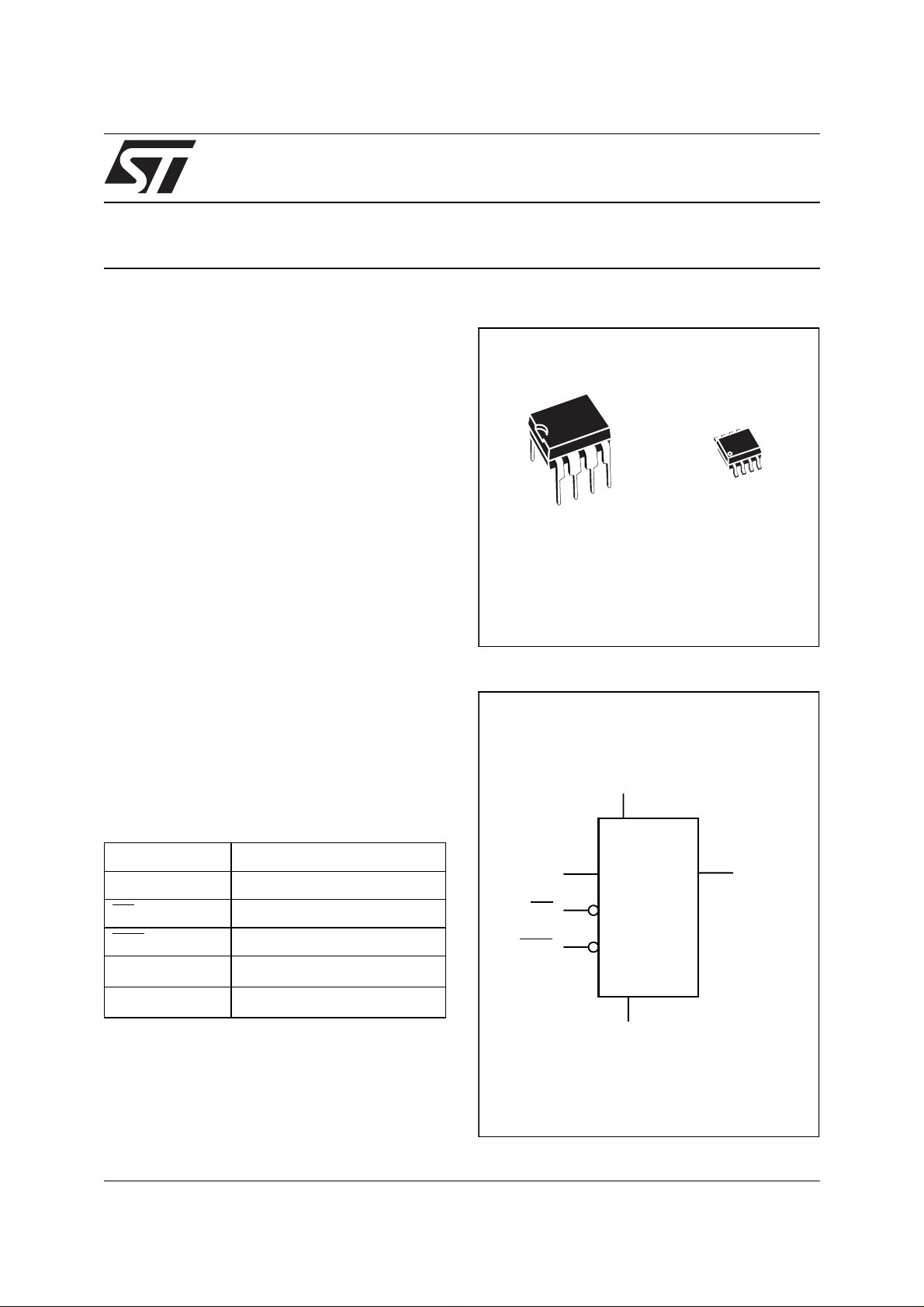
Figure 1. Delivery Forms
8
1
PSDIP8 (BN)
0.25 mm Frame
Figure 2. Logic Diagram
V
CC
8
1
S08 (MN)
150 mil Width
Table 1. Signal Names
SDA Serial Data Address Input/Output
SCL Serial Clock
WC
WCR
Write Control of Control Register
V
CC
V
SS
This is a Preliminary Data. Details are subject to change without notice.
Write Control
Supply Voltage
Ground
SCL
WC
WCR
M34S32
V
SS
SDA
AI02468
1/18June 1998
Page 2
M34S32
Figure 3. DIP Pin Connections
M34S32
1
NC V
2
SS
3
4
WCR
8
7
6
5
AI02448
CC
WCNC
SCL
SDAV
Table 2. Absolute Maximum Ratings
(1)
Figure 4. SO Pin Connections
M34S32
NC V
1
2
WCR
SS
3
4
8
7
6
5
AI02449
CC
WCNC
SCL
SDAV
Symbol Parameter Value Unit
T
T
A
STG
Ambient Operating Temperature –40 to 125 °C
Storage Temperature –65 to 150 °C
Lead Temperature, Soldering (SO8 package) 40 sec 215 °C
T
LEAD
(PSDIP8
package)
10 sec 260 °C
V
IO
V
CC
Input or Output Voltages –0.6 to 6.5 V
Supply Voltage –0.3 to 6.5 V
(Human Body model)
Electrostatic Discharge Voltage
V
ESD
Electrostatic Discharge Voltage
Note: 1. Except for the ra ting “Op era ting T em perat ure Ra nge ”, s tresse s abov e tho se lis ted in t he Tab le “ A bsolut e M axi mum R ati ngs”
may cause perm ane nt damag e to th e devic e. T hese ar e str ess ra tin gs only and o perat ion of t he de vice at thes e or any other
conditions above those indi cated in th e Operating section s of this specification is not implied. E xposure to Absolut e M aximum
Rating conditions for extended periods may a ffect device r eliability. R efer a lso to the STMicroelectronics SURE Program and
other relevant quality documents.
1. MIL-STD-883C, 3015.7 (100 pF,
1500 Ω)
(Machine model)
2. EIAJ IC-121 (Condition C)
(200 pF, 0 Ω)
4000 V
500 V
2/18
Page 3

M34S32
DESCRIPTION (cont’d)
2
The memory is compatible with t he I
C extended
addressing standard, two wire serial interface
which uses a bi-directional data bus and serial
clock. The memory carries a built-in 4 bit, unique
device identification code (1010) corresponding to
2
the I
C bus definition. The memory behaves as
slave devices in the I
2
C protocol with all memory
operations synchronized by the serial clock. Read
and write operations are initiated by a START condition generated by the bus m aster. The START
condition is followed by the Device Select Byte.
This is a stream o f 4 bits (the identification c ode
1010), then 3 bits o f memory block access input,
plus one read/write bit. The byte is finally terminated by an acknowledge bit.
The M34S32 contains three memory blocks: the
OTP page, the EEPROM block and the ROM
block. The OTP (One T ime Programmab le) page
is a page of 32 bytes, written once by the user. The
OTP page is not located within the 32 Kbits EEPROM area. Once written, the OTP page cannot be
modified by further write instructions. The ROM
block resides inside the 32 Kbit EEPROM area.
The size of the ROM block is defined (by the user)
with the help of the Control Register.
The OTP page is accessed with the Device Select
Byte 1010001x, the EEPROM and ROM blocks
are accessed with the Device Select Byte
1010000x. The con trol register is accessed with
the Device Select Byte 1010100x (see Table 3).
Table 3. Device Select Byte
When writing data to the memory it responds to
the 8 bits received by asserting an acknowledge
bit during the 9th bit time. When data is read by the
bus master, it acknowledges the receipt of the
data bytes in the same way.
Data transfers are terminated with a STOP condi tion.
Power On Reset: VC C lock out wri te protect. In
order to prevent data corrup tion and inadvertent
write operations during power up, a Power On Reset (POR) circuit is implemented. Until the VCC
voltage has reached the POR threshold value, the
internal reset is active: all operations are disabled
and the device will not respon d to any comma nd.
In the same way, when VCC drops down from the
operating voltage to below the POR threshold value, all operations are disabled and the device will
not respond to any command. A stable VCC must
be applied before applying any logic signal.
SIGNAL DESCRIPTION
Serial Clock (SCL). Th e SC L input pin is used to
synchronize all data in and out of the memory. A
resistor can be connected from the SCL line to
VCC to act as a pull up (see Figure 3)
Serial Data (SDA). The SDA pin is bi-directional
and is used to transfer data in or out of the memory. It is an open drain output that may be wire-
OR’ed with other open drain or open collector signals on the bus. A pull-up resistor must be connected from the SDA bus line to V
(see Figure
CC
3).
Device Code Memory Block Access RW
Device Select Bit b7 b6 b5 b4 b3 b2 b1 b0
EEPROM and ROM access 1 0 1 0 0 0 0 RW
OTP Page access 1 0 1 0 0 0 1 RW
Control Register access 1 0 1 0 1 0 0 RW
Table 4. Operating Modes
Mode RW bit
Current Address Read 1 1 START, Device Select, RW
0
Random Address Read
1 reSTART, Device Select, RW
Sequential Read 1 ≥ 1 As CURRENT or RANDOM Mode
Byte Write 0 1 START, Device Select, RW
Page Write 0 ≤ 32 START, Device Select, RW
3/18
Data
Bytes
1
Initial Sequence
START, Device Select, RW
= 1
= 0, Address
= 1
= 0
= 0
Page 4
M34S32
Write Control (WC). The Write Control feature
is useful to protect the conte nts of the whole
WC
EEPROM area from any erroneous erase/write cycle. It also protects the OTP page ag ainst the first
write attempt. The Write Control signal polarity can
be selected with the WCpol bit of the Control Register (see Table 13). When pin WC
ed, the WC
input is internally read as VIL (see
is unconnect-
Table 5).
When WC
and WCpol are activating the Write Protection, Device Select and Address byte s are acknowledged; Data bytes are not acknowledged
(see Figure 11).
Write Control (WCR
). In order to prevent spurious
writes to the Control Regi ster, the user can also
make the Control Register Read Only (Write is inhibited). This is achieved by use of the WCR
pin
and the CRWD bit (see Table 14) :
– - if CRWD b it = 0, the Control register can be
modified regardless of the state of the WCR
pin.
– - if CRWD bit = 1, the C ontrol register can be
modified if the WCR
– - i f CRWD bit = 1 and the WCR
pin is high.
pin is low, the
Control Register is Write Protected.
DEVICE OPERATION
2
C Bus Background
I
The memory supports the extended addressing
2
I
C protocol. This protocol defines any device that
sends data onto the bus as a t ransmitter and any
device that rea ds the data as a rec eiver. The de vice that controls the data transfer is known as the
master and the other as the slave. The master will
always initiate a data transfer and will provide the
serial clock for synchronisation. The memory is always a slave device in all communications.
Start Condition. START is identified by a high to
low transition of the S DA line while the clock SCL
is stable in the high state. A START condition must
precede any command for data transfer. E xcept
during a programming cycle , the memory con ti n uously monitors the SDA and SCL signals for a
START condition and will not respond unless one
is given.
Stop C ondition. STOP is identified by a low to
high transition of the SDA line while the clock SCL
is stable in the high state. A STOP condition terminates communication between the memory and
the bus master. A STO P c ondi tion at the end of a
Read command forces the stand-by state. A
STOP condition at the end of a Write command
triggers the internal EEPROM write cycle.
Acknowledge Bit (ACK). An ac knowled ge s ignal
is used to indicate a successful data transfer. The
bus transmitter, either master or slave, will release
the SDA bus after send ing 8 bits of data. During
the 9th clock pulse the receiver pulls the SDA bus
low to acknowledge the receipt of the 8 bits of data.
Data Input. During data input the memory samples the SDA bus signal on the rising edg e of the
clock SCL. For correct device operation the SDA
signal must be stable during the clock low to high
transition and the data must c hange ONLY when
the SCL line is low.
Device Selection. To start communication between the bus master an d the slav e memory , the
master must initiate a START condition. The 8 bits
sent after a START condition are made up of a Device Select Byte of 4 bits that identifie s the devi ce
type, 3 memory block access bits and one bit for a
READ (RW
= 1) or WRITE (RW = 0) operation.
There are two modes both for read and write.
These are summarised in Table 4 and described
hereafter. Communication between the master
and the slave is ended with a STOP condition.
(1)
Table 5. Input Parameters
(T
= 25°C, f = 400 kHz)
A
Symbol Parameter Test Condition Min. Max. Unit
C
C
Z
Z
t
LP
Note: 1. Sampled only, not 100% tested in production.
Input Capacitance (SDA) 8 pF
IN
Input Capacitance (other pins) 6 pF
IN
WC, WCR Input Impedance
L
WC, WCR Input Impedance
H
Low-pass filter input time constant (SDA and SCL) 100 ns
V
IN
V
IN
≤ 0.3 V
≥ 0.7 V
CC
CC
520kΩ
500 kΩ
4/18
Page 5

Figure 5. Maximum RL Value versus Bus Capacitance (CBUS) for an I2C Bus
V
20
16
12
8
Maximum RP value (kΩ)
4
0
10 1000
C
BUS
fc = 400kHz
100
(pF)
fc = 100kHz
CC
MASTER
SDA
SCL
R
L
C
M34S32 -
R
L
BUS
AI01665
C
BUS
Table 6. DC Characteristics (T
= 0 to 70°C, –40 to 85°C; VCC = 4.5V to 5.5V, 2.5V to 5.5V)
A
Symbol Parameter Test Condition Min. Max. Unit
I
LI
I
LO
I
CC
I
CC1
I
CC2
V
IL
V
IH
V
IL
V
IH
V
OL
Input Leakage Current (SCL,
SDA)
Output Leakage Current
Supply Current
Supply Current (W series)
Stand-by Current
Stand-by Current (W series)
Input Low Voltage (WC
Input High Voltage (WC
, WCR) – 0.3 0.5 V
, WCR)
0 ≤ VIN ≤ V
0 ≤ V
V
CC
CC
≤ VCC; SDA in Hi-Z
OUT
= 5 V; fC = 400 kHz
(rise/fall time < 30 ns)
V
= 2.5 V; fC = 400 kHz
CC
(rise/fall time < 30 ns)
VIN = VSS or VCC ; VCC = 5 V
= VSS or VCC ; VCC = 2.5 V
V
IN
Input Low Voltage (other pins) – 0.3
Input High Voltage (other pins)
= 3 mA, VCC = 5 V
Output Low Voltage
Output Low Voltage (W series)
I
OL
= 2.1 mA, VCC = 2.5 V
I
OL
±2 µA
±2 µA
2 mA
1 mA
10 µA
2 µA
- 0.5 VCC + 1
V
CC
0.3 VCC
0.7 VCC VCC + 1
0.4 V
0.4 V
V
V
V
5/18
Page 6
M34S32
Table 7. AC Measurement Conditions
Input Rise and
Fall Times
Input Pulse
Voltages
≤ 50ns
0.2 V
to 0.8 V
CC
CC
Figure 6. AC Testing Input/Output Waveforms
0.8V
CC
0.2V
CC
Input and Output
Timing Reference
0.3 V
to 0.7 V
CC
CC
Voltages
Table 8. AC Characteristics (TA = 0 to 70 °C,
–40 to 85°C; V
Symbol Alt. Parameter
t
CH1CH2
t
CL1CL2
t
t
t
t
t
t
t
t
t
t
t
t
f
t
Note: 1. Sampled only, not 100% tested in production.
(1)
DH1DH2
(1)
DL1DL2
(2)
CHDX
CHCL
DLCL
CLDX
CLCH
DXCX
CHDH
DHDL
(3)
CLQV
QLQx
C
W
2. For a reS T AR T condition , or following a write cy cle.
3. The minimum value delays the falling/rising edge of SDA away from SCL=1 in order to avoid unwanted START and/or STOP
conditio ns .
= 4.5V to 5.5V, 2.5V to 5.5V)
CC
t
Clock Rise Time 300 300 ns
R
t
Clock Fall Time 300 300 ns
F
t
SDA Rise Time 20 300 20 300 ns
R
t
SDA Fall Time 20 300 20 300 ns
F
t
SU:STA
t
HIGH
t
HD:STA
t
HD:DAT
t
t
SU:DAT
t
SU:STO
t
f
t
LOW
BUF
t
AA
t
DH
SCL
WR
Clock High to Input Transition 600 600 ns
Clock Pulse Width High 600 600 ns
Input Low to Clock Low (START) 600 600 ns
Clock Low to Input Transition 0 0 µs
Clock Pulse Width Low 1300 1300 ns
Input Transition to Clock Transition 100 100 ns
Clock High to Input High (STOP) 600 600 ns
Input High to Input Low (Bus Free) 1300 1300 ns
Clock Low to Next Data Out Valid 200 900 200 900 ns
Data Out Hold Time 200 200 ns
Clock Frequency 400 400 kHz
Write Time 10 10 ms
M34S32
V
= 4.5V to
CC
5.5V
VCC = 2.5V to
5.5V
Min. Max. Min. Max.
0.7V
0.3V
AI00825
Unit
CC
CC
6/18
Page 7

M34S32
EEPROM Addressing. A data byte in the memory
is addressed through 2 bytes of addres s information. The Most Significant Byte is sent first and the
Least significant By te is sen t after. Bits b15 to b0
form the address of any byte of the memory. Bits
b15 to b12 are don’t care on the M34S32 series.
Table 9. Most Significant Byte
b15 b14 b13 b12 b11 b10 b9 b8
XXXX
4. b15 to b12 are Don’t Care.
Table 10. Least Significant Byte
b7 b6 b5 b4 b3 b2 b1 b0
Figure 7. AC Waveforms
tCHCL
SCL
tDLCL
SDA IN
tCHDX
tCLDX
Write Operations
Following a START condition the m aster sends a
Device Select Byte with the RW
bit reset to 0. The
memory acknowledges t his and waits for 2 bytes
of address. These 2 address bytes (8 bits each)
provide access to any of the memory location.
Writing in the memory may be inhibited with WC
pin and WCpol bit (see Table 13 and Figure 11).
tCLCH
tDXCX
tCHDH
tDHDL
SCL
SDA OUT
SCL
SDA IN
START
CONDITION
tCLQV tCLQX
DATA OUTPUT
tCHDH
STOP
CONDITION
SDA
INPUT
DATA VALID
WRITE CYCLE
CHANGE
tW
SDA
STOP &
BUS FREE
tCHDX
START
CONDITION
AI00795B
7/18
Page 8

M34S32
Byte Write. In the Byte Write mode the master
sends one data byte, which is acknowledged by
the memory. The master then terminates the
transfer by generating a STOP condition.
Page Write. The Page Write mode allows up to 32
bytes to be written in a single writ e cyc le, provided
that they are all located in the same row of 32
bytes in the memory, that is the same Address bits
(b12 to b5). The master sends one up t o 32 byt es
of data, which are each acknowledged by the
memory. After each b yte is transferred, the internal byte address counter (5 Le ast Significant Bits
only) is incremented. The transfer is t erminated by
the master generating a STOP condition. Care
must be taken to avoid address counter “roll-over”
which could result in data being overwritten.
2
Figure 8. I
C Bus Protocol
SCL
SDA
Note that for any write mode, the generation by the
master of the STOP condition starts the internal
memory program cycle. This STOP condition will
trigger an internal memory program cycle only if
the STOP condition is i nternally decoded right af ter the ACK bit; any STOP condition decode d out
of this “10th bit” time slot will not trigger the internal
programming cycle. All inputs are disabled until
the completion of this cycle and the Memory will
not respond to any request.
SCL
SDA
SCL
SDA
START
CONDITION
START
CONDITION
SDA
INPUT
1 23 789
MSB
1 23 789
MSB ACK
SDA
CHANGE
CONDITION
ACK
STOP
STOP
CONDITION
AI00792
8/18
Page 9

M34S32
Write to the Control Register
The control register is access ed using a specific
Device Select Byte (as described in Table 3, and
as shown in Table 11 and Table 12).
Table 11. Content of the Control Register
b7 b6 b5 b4 b3 b2 b1 b0
CRWD WCpol X B2 B1 B0 X X
Table 12. Default values
b7 b6 b5 b4 b3 b2 b1 b0
00X000XX
The meanings of the bits in Table 11 can be summarised as follows:
WCpol. This bit controls the polarity of the WC input (to switch pin 7 between being a WC or WC
in-
put). The default (initial) state of this bit is 0.
Table 13. Operation of the WCpol Bit
pin 7 = high pin 7 = low
Write instructions
are allowed in the
EEPROM area,
and the OTP
page can be
written once
Whole EEPROM
and OTP page are
write protected
WCpol = 0
WCpol = 1
Whole EEPROM
and OTP page are
write protected
Write instructions
are allowed in the
EEPROM area,
and the OTP
page can be
written once
CRWD. This is the Control Register Write Disable
bit. When it is 0, pin 3 is a Don’t Care input, and the
control register is always writable. This is the default (initial) condition of this bit.
Table 14. Operation of the CRWD Bit
pin 3 = high pin 3 = low
CRWD = 0 Control register is writable
Control register is
write protected
(read only)
CRWD = 1
Control register is
writable
B2,B1,B0. These bits control the size of the ROM
block. Their initial, default state is 0, 0, 0.
Table 15. Operation of the B2, B1 and B0 Bits
B2,B1,B0 ROM block size and location
0,0,0 0 All bits are EEPROM
0,0,1 1/64 ROM block=00h to 01FFh (512)
0,1,0 1/32 ROM block=00h to 03FFh (1K)
0,1,1 1/16 ROM block=00h to 07FFh (2K)
1,0,0 1/8 ROM block=00h to 0FFFh (4K)
1,0,1 1/4 ROM block=00h to 1FFFh (8K)
1,1,0 1/2 ROM block=00h to 3FFFh (16K)
1,1,1 1 All bits are ROM
In all cases, except when (B2,B 1,B0)=(0,0,0), the
selected area of EEPROM becomes read only
(Write Protected) regardless of the status of the
other bits and pins. However, the Control Register
itself remains alterable in accordance with the status of WC
, WCpol, WCR and CRWD.
Write to the OTP Page
The OTP page is accessed by addressing the device using the spe ci fic, Device Select Byte (as described in Table 3).
The correct sequence for this instruction can be
sketched out as follows:
Start
OTP Page Select(= 1010 0010)
Ack
Address (MSB) (= xxxx 0000)
Ack
Address (LSB) (= 0000 0000)
Ack
Data (= byte to be written)
Ack
........
Data (= byte to be written)
Ack
Stop
If one bit of the OT P Page S elect differs f rom the
above values, the OTP Page Select will NOT be
acknowledged and the WRITE instruction will be
ignored.
9/18
Page 10

M34S32
If one bit of the Address bytes (excluding the three
most significant bits which are Don’t Care) differs
from the above values, the Address will be acknowledged, data will not be acknowledged and
the WRI TE ins tru c t ion w ill be ignored.
The Page Write instruction must start with the first
byte that is located in the OTP page (address 0h),
otherwis e the instruct io n w ill b e ig nored.
The first Write to the OTP page (whether it be a 1byte write, a 32-byte page w rite, or some size in
between) will disable any further write in the OTP
page.
Let us suppose that byte N of the OTP page has
just been addressed (for example because of a
Write in the OTP page or a Random read in the
OTP page). If the next instruction uses the Current
Read Mode of the device, the first byte read in
EEPROM will be in page 0, at address N+1 (or
page 1, byte 0 if the last OTP byte addressed was
at location 31).
Figure 9. Write Cycle Polling using ACK
WRITE Cycle
in Progress
Example of a correct sequence, leading to a 3byte write in the OTP page:
Start
1010 0010 (OTP page select code)
Ack
1111 0000 (upper address, MSB)
Ack
0000 0000 (lower address, LSB)
Ack
0100 1101 (write 3 bytes of data)
Ack (in the OTP page)
1100 1010
Ack
0101 0011
Ack
Stop
First byte of instruction
with RW = 0 already
decoded by M34Sxx
ReSTART
STOP
START Condition
DEVICE SELECT
with RW = 0
ACK
NO
Returned
YES
Next
Operation is
Addressing the
Memory
WRITE Operation
YESNO
Proceed
Send
Byte Address
Proceed
Random Address
READ Operation
AI02418
10/18
Page 11

M34S32
Example of an incorrect sequence, disabling the
Write in the OTP page:
Start
1010 0010 (OTP page select code)
Ack
xxxx 0000 (MSB address)
Ack
0000 0100 (incorrect LSB address)
Ack (acknowledged, but...)
0100 1101 (the attempts at)
(no ack) (writing data to the)
1100 1010 (OTP page are)
(no ack) (not acknowledged)
0101 0011
(no ack)
Stop
Figure 10. Write M ode s S equence with WC
= 0
and WCpol = 0
WC
ACK
Minimizing System Delay by Polling On ACK.
During the internal Write cycle, the memory disables itself from the bus in order to copy the data
from the internal latches to the memory cells. The
maximum value of the Write time (t
) is given in
W
the AC Characteristics table, this timing value may
be reduced by an ACK polling sequence issued by
the master.
The sequence is:
– Initial condition: a Write i s in progress (see Figure 7).
– Step 1: the Master issues a START condition followed by a Device Select Byte. (1st byte of the
new instruction)
– Step 2: if the memory is internally writing, no
ACK will be returned. The Master goes back to
Step1. If the memory has terminated t he internal
writing, it will issue an ACK.
The memory is ready to receive the second part of
the instruction (the first byte of this instruction was
already sent during Step1).
ACK ACK ACK
BYTE WRITE DEV SEL BYTE ADDR BYTE ADDR DATA IN
R/W
START
WC
ACK ACK ACK ACK
PAGE WRITE DEV SEL BYTE ADDR BYTE ADDR DATA IN 1
R/W
START
WC (cont'd)
ACKACK
PAGE WRITE
(cont'd)
DATA IN N
STOP
STOP
DATA IN 2
Note: 1. The devi ce has the sam e behavior w hen WC = 1 a nd
WCpol = 1.
11/18
AI01106B
Page 12

Figure 11. Write M ode s S equence with WC = 1
and WCpol = 0
WC
ACK ACK ACK NO ACK
BYTE WRITE DEV SEL BYTE ADDR BYTE ADDR DATA IN
M34S32
R/W
START
WC
ACK ACK ACK NO ACK
PAGE WRITE DEV SEL BYTE ADDR BYTE ADDR DATA IN 1
R/W
START
WC (cont'd)
NO ACK NO ACK
PAGE WRITE
(cont'd)
Note: 1. The devi ce has the sam e behavior w hen WC = 0 a nd
WCpol = 1.
DATA IN N
STOP
Read Operations
On delivery, the memory content is s et at all “1”s
(or FFh).
Current Address Read. The memory has an internal address counter. Each time a byte is read,
this counter is incremented. For the Current Address Read mode, f ollowing a START condition,
the master sends a Device Select Byte with the
bit set to 1. The memory acknowledges this
RW
and outputs the byte addressed by the internal address counter. This counter is then incremented.
The master does NOT acknowledge the byte output, but terminat es t he t ransfe r wi th a S TO P c on dition.
A Current Address Read in the OTP page is performed by sending the appropria te Device Select
Byte, as described in Table 3.
STOP
DATA IN 2
AI01120B
Let us suppose, again, that byte N of the OTP
page has ju st been address ed (for example because of a Write in the OTP page or a Rand om
read in the OTP page). If the next instruction uses
the Current Address Read Mode of the device, the
first byte read in EEPRO M will be in page 0, at address N+1 (or page 1, byte 0 if the l ast OTP byte
addressed was at location 31).
Random Address Read. A dum my write is performed to load the address into the address counter, see Figure 10. This is followed by another
START condition from the master and the byte address repeated with the RW
bit set to 1. The memory acknowledges this and outputs the byte
addressed. The master does NOT acknowledge
the byte o utput, but term inates the trans fer with a
STOP condition.
Specific features of the Random Address read
in the OTP page. This instruction must consist of
the two sequences show n on page 14 (Sequence
A followed by Sequence B).
12/18
Page 13

M34S32
Figure 12. Read Mode Sequences
CURRENT
ADDRESS
READ
RANDOM
ADDRESS
READ
SEQUENTIAL
CURRENT
READ
SEQUENTIAL
RANDOM
READ
ACK
DEV SEL DATA OUT
R/W
START
ACK
DEV SEL * BYTE ADDR BYTE ADDR
R/W
START
ACK ACK ACK NO ACK
DEV SEL DATA OUT 1
R/W
START
ACK ACK ACK
DEV SEL * BYTE ADDR BYTE ADDR
NO ACK
STOP
ACK ACK ACK
DEV SEL * DATA OUT
R/W
START
DATA OUT N
STOP
ACK ACK
DEV SEL * DATA OUT 1
NO ACK
STOP
R/W
START
ACK NO ACK
DATA OUT N
STOP
Note: 1. The seven most sign ifi cant bits of the DEV SEL code of
a Rando m Read (1st byte an d 4th byte) must be identi cal.
R/W
START
AI01105C
13/18
Page 14

M34S32
Sequence A:
Start
OTP Page Select(= 1010 0010)
Ack
Address MSB (= xxxx 0000)
Ack
Address LSB (= 000x xxxx)
Ack
Sequence B:
Start
OTP Page Select(= 1010 0011)
Ack
Data
Ack
........
Data
(no Ack)
Stop
If one, or more bits of the Sequen ce A dif fer from
the above values, the bytes that follow it will be acknowledged (or not) according to the sam e rules
as for the WRITE IN OTP, and the RA NDOM A DDRESS READ IN OTP will be ig nor e d .
Sequential Read. This mode can be initiated with
either a Current Address Re ad or a Random Address Read. However, in this case the master
DOES acknowledge the data byte output and the
memory continues to o utput the next byte in sequence. To terminate the stream of bytes, the
master must NOT acknowledge the last byte output, but MUST generate a STOP condition.
The output data is from consecutive byte addresses, with the internal byte address counter automatically incremented after each byte output. After a count of the last memory address, the
address counter will “roll-over” and the memory
will continue to output data.
A Sequential Read in the OTP pa ge is performed
by sending the appropriate Device Select Byte, as
described in Table 3. If a seque ntial read rea ch es
the last location in the O TP page (address 1Fh),
subsequent Sequential Reads will wrap round to
the start, to address 00h.
Acknowledge in Read Mode. In all read modes
the memory waits for a n acknowledge during the
9th bit time. If the master does not pull the SDA
line low during this time, the memory terminates
the data transfer and switches to a stand-by state.
APPLICATION HINTS ON HOW TO USE THE
CONTROL REGISTER TOGETHER WITH THE /
WCR PIN
The application board can be designed in such a
way that WCR
pin is connected to VSS (directly or
through a pull-down resistor). It should be noted
that the WCR
pin features an internal pull-down resistor allowing this inpu t to be le ft unconnected.
With such a P.C.B. (Printed Circuit Board), the device can be initialised according to following set-up
sequence :
1. Write the data that is to be Write protected:
– Write data in the area starting from address
00h up to the desired address.
2. Write in the Control Register (single byte write
using the following bits):
– S et B2, B 1 and B0 values a ccording to the
ROM block size (as defined in Table 15)
– Set WCpol according to the application
needs.
– Set CRWD bit to 1
Once the CRWD bit is set to 1, the control register
becomes Write Protected. The only way to write
again to the Control Register is to set the WCR
high. This is possible by applying V
to WCR if it
CC
was previously floating or connected to V
pin
SS
through an external pull -down resistor. If WCR is
shorted to V
, the device needs to be de-sol-
SS
dered from the PCB.
OTHER NOTES
The WCR
pin has an internal pull-down resistor.
Connecting this pin to GND does not affect the
power consumption, thus giving the M34S32 its
lowest power consumpt ion when it is i n P rot ected
mode.
The OTP page may be programmed before or after the hardware protected mode has been set (by
setting the CRWD bit). This allows the a pplication
MCU to program the OTP page either on the assembly line or during the operating life of the application.
The WC
pin (but not the WCR pin) may be driven
dynamically by the MCU to i ncreas e the im m unity
to data corruption of the unprotected EEPROM area. This pin may alternatively be pulled to V
CC
or
GND (depending on which is appropriate, according to the setting of the WCpol bit).
14/18
Page 15

M34S32
ORDERING INFORMATION SCHEME
Devices are shipped from the factory with the
memory content set at all “1”s (FFh).
For a list of available options, refer to the current
Memory Shortform Catalogue
Example:
Capacity
32: 32 Kb (4Kx8)
Note: 1. Temperature range 1 i s available on request onl y.
.
M 34 S 32 - W MN 1 T
Supply Voltage
blank: 4.5 to 5.5 V
W: 2.5 to 5.5 V
BN: PSDIP8
0.25 mm frame
150 mil body width
For further information on any aspect of this device, please contact the ST Sales Office nearest to
you.
In general, the fields of the product number are
made up as follows:
Package
MN: SO8
Temp. Range
1: 0 to 70 oC
6: -40 to 85 oC
5: -20 to 85 oC
(see note 1)
Option
T: Tape & Reel
Packing
AI02469
15/18
Page 16

Table 16. PSDIP8 - 8 pin Plastic Skinny DIP,
0.25mm lead frame
M34S32
Symb.
mm inches
Typ. Min. Max. Typ. Min. Max.
A 3.90 5.90 0.154 0.232
A1 0.49 – 0.019 –
A2 3.30 5.30 0.130 0.209
B 0.36 0.56 0.014 0.022
B1 1.15 1.65 0.045 0.065
C 0.20 0.36 0.008 0.014
D 9.20 9.90 0.362 0.390
E 7.62 – – 0.300 – –
E1 6.00 6.70 0.236 0.264
e1 2.54 – – 0.100 – –
eA 7.80 – 0.307 –
eB 10.00 0.394
L 3.00 3.80 0.118 0.150
N8 8
Figure 13. PSDIP8
Note: 1. Note: Drawing is not to scale.
A2
A1AL
B
N
1
e1
B1
D
E1 E
eA
eB
C
PSDIP-a
16/18
Page 17

M34S32
Table 17. SO8 - 8 lead Plastic Small Outline,
150 mils body width
Symb.
mm inches
Typ. Min. Max. Typ. Min. Max.
A 1.35 1.75 0.053 0.069
A1 0.10 0.25 0.004 0.010
B 0.33 0.51 0.013 0.020
C 0.19 0.25 0.007 0.010
D 4.80 5.00 0.189 0.197
E 3.80 4.00 0.150 0.157
e 1.27 – – 0.050 – –
H 5.80 6.20 0.228 0.244
h 0.25 0.50 0.010 0.020
L 0.40 0.90 0.016 0.035
α 0° 8° 0° 8°
N8 8
CP 0.10 0.004
Figure 14. SO8a
B
SO-a
Note: 1. Note: Drawing is not to scale.
h x 45˚
A
e
D
N
1
CP
E
H
C
LA1 α
17/18
Page 18

M34S32
Information furnished is believed to be ac curate and reli able. Howev er, STMicroel ectronic s assumes no res ponsibility for the consequences
of use of such information nor for any infringement of patents or other rights of third parties which may result from its use. No license is granted
by implic ation or otherwise under any patent or patent rights of STMi croelect ronics. Specifications mentioned in thi s publica tion are subject
to change without notice. This publication supersedes and replaces all information previously supplied. STMicroelectronics products are not
authoriz ed for use as critical components in li fe support devices or sy stems without expre ss wri tten appr oval of STMic roelectronics.
© 1998 STM i croelectronics - All Ri ghts Reser ved
The ST logo is a registered trademark of STMicroelectron i cs .
All other names are the property of their respective owners.
STMicroele ctronics GROUP OF COMPANIES
Australia - Brazil - Chi na - Franc e - Germany - Italy - Japan - Ko rea - Malays ia - Malta - Mex i co - Morocco - T he Netherlands - Singapore -
Spain - Sweden - Switz erl and - Taiwan - Thailand - United Kingdom - U.S. A.
18/18
 Loading...