

Page 1
FEATURES SUMMARY
■ Software Data Protection for lower 128 bytes
■ Two Wire I
■ 100kHz and 400kHz Transfer Rates
■ Single Supply Voltage:
2
C Serial Interface
– 2.5 to 5.5V up to 400kHz for M34C02-W
– 2.2 to 5.5V up to 400kHz for M34C02-L
– 1.8 to 5.5V up to 100kHz for M34C02-R
– 1.7 to 3.6V up to 100kHz for M34C02-F
■ BYTE and PAGE WRITE (u p to 16 by te s)
■ RANDOM and SEQUENTIAL READ Modes
■ Self-Tim e d P rogramming Cyc le
■ Automatic Address Incrementing
■ Enhanced ESD/Latch-Up Protection
■ More than 1 Million Erase/Write Cycles
■ More than 40 Year Data Retention
M34C02
2 Kbit Serial I²C Bus EEPROM
For DIM M Serial P resence Detect
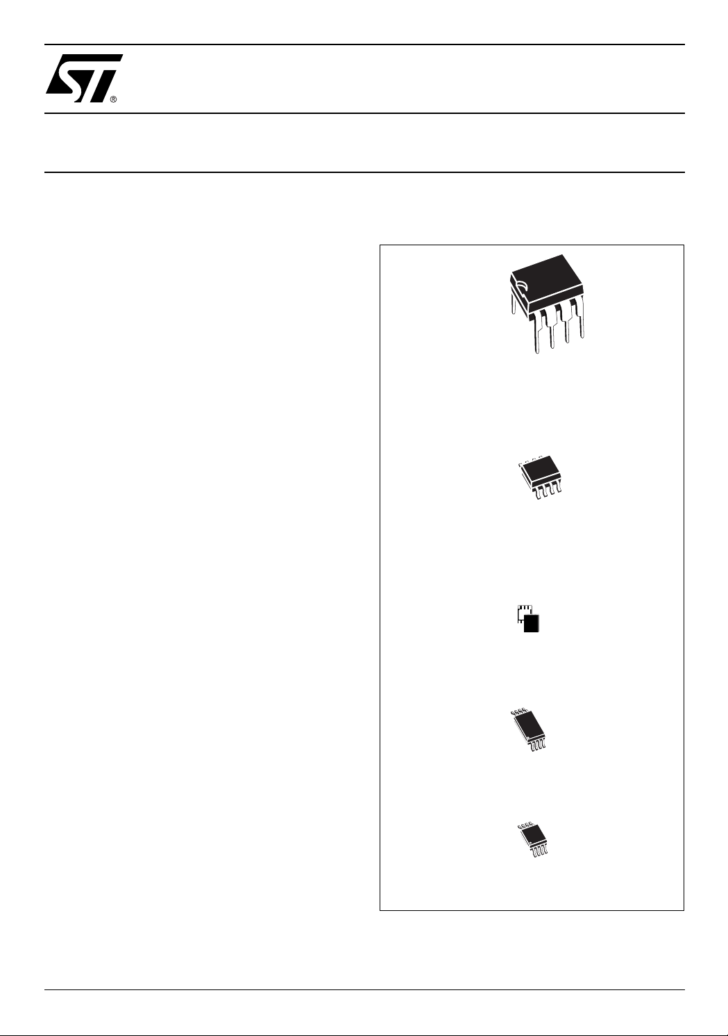
Figure 1. Packages
8
1
PDIP8 (BN)
8
1
SO8 (MN)
150 mil width
VFDFPN8 (MM)
2x3mm² (MLP)
TSSOP8 (DW)
169 mil width
TSSOP8 (DS)
3x3mm² body size (MSOP)
1/26July 2003
Page 2
M34C02
SUMMARY DESCRIPTION
The M34C02 is a 2 Kbit serial EEPROM memory
able to lock permanently the data in its first half
(from location 00h to 7Fh). This facility has been
designed specifically for use in DRAM DIMMs
(dual interline memory modules) with Serial
Presence Detect. All the information concerning
the DRAM module configuration (such as its
access speed, its size, its organization) can be
kept write protected in the first half of the memory.
This bottom half of the memory area can be writeprotected using a specially designed software
write protection mechanism. By sending the
device a specific sequence, the first 128 bytes of
the memory become permanently write protected.
Care must be taken w hen us i ng this s equence as
its effect cannot be reversed. In addition, the
device allows the entire m emory area to be write
protected, using the WC input (for example by
tieing this input to V
2
These I
C-compatible electrically erasable
programmable memory (EEPROM) devices are
organized as 256x8 bits.
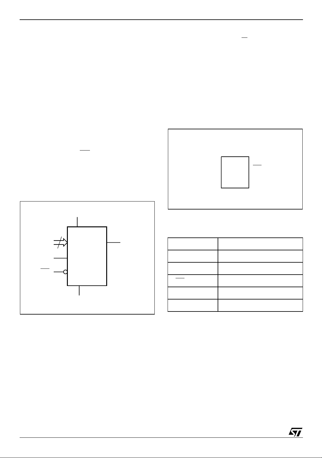
Figure 2. Logic Diagram
CC
).
Device Select Code and RW
bit (as described in
Table 2), terminated by an acknowledge bit.
When writing data to the memory, the memory
inserts an acknowledge bit during the 9
th
bit time,
following the bus master’s 8-bit transmission.
When data is read by the bus master, the bus
master acknowledges the receipt of the data byte
in the same way. Data transfers are terminated by
a STOP condition after an Ack for WRITE, and
after a NoAck for READ.
Figure 3. DI P, SO, TSSOP and VF D FPN Connections (Top View)
M34C02
1
E0 V
2
3
E2
4
SS
8
7
6
5
AI01932C
CC
WCE1
SCL
SDAV
V
CC
3
E0-E2 SDA
SCL
WC
2
C uses a tw o wire serial i nterface, comprising a
I
M34C02
V
SS
AI01931
bi-directional data line and a clock line. The device
carries a built-in 4-bit Device Type Identifier code
(1010) in accordance with the I
2
C bus definition to
access the memory area and a second Device
Type Identifier Code (0110) to access the
Protection Register. These codes are used
together with three chip enable inputs (E2, E1, E0)
so that up to eight 2 Kbit devices may be attached
to the I²C bus and selected individually.
The device behaves as a slave device in the I
2
protocol, with all memory operations synchronized
by the serial clock. Read and Write operations are
initiated by a START condition, gene rated by the
bus master. The START condition is followed by a
Note: 1. Se e the pages after page 19 for package dimens ions,
and how to ide ntify pin-1.
Table 1. Signal Names
E0, E1, E2 Chip Enable
SDA Serial Data
SCL Serial Clock
WC
V
CC
V
SS
Power On Reset: V
Write Control
Supply Voltage
Ground
Lock-Out Write Protect
CC
In order to prevent data corruption and inadvertent
Write operations during power up, a Power On
Reset (POR) circuit is included. The internal reset
is held active until V
has reached the POR
CC
threshold value, and all operations are disabled –
the device will not respond to any command. In the
same way, when V
drops from the operating
CC
voltage, below the POR threshold value, all
operations are disabled and the device will not
C
respond to any command.
A stable and valid V
(as defined in Tables 6 to
CC
9) must be applied before applying any logic
signal.
2/26
Page 3
SIGNAL DESCRIPTION
Serial Clock (SCL)
This input signal is used to strobe all data in and
out of the device. In applications where this signal
is used by slave devices to synchronize the bus to
a slower clock, the bus master must have an open
drain output, and a pull-up resistor can be connected from Serial Clock (SCL) to V
. (Figure 4
CC
indicates how the valu e of the p ull-up resistor c an
be calculated). In most applications, thoug h, this
method of synchronization is no t employed, and
so the pull-up resistor is not necessary, provided
that the bus maste r has a push-pull (rather than
open drain) output.
Serial Data (SDA)
This bi-directional signal is used to transfer data in
or out of the device. It is an open drain output that
may be wire-OR’ed with other open drain or open
collector signals on the bus. A pull up resistor must
be connected from Serial Data (SDA) to V
CC
. (Fig-
M34C02
ure 4 indicates how the value of the pull-up resistor
can be calculated).
Chip Enable (E0, E1, E2)
These input signals are used to set the value that
is to be looked for on the three least significant bits
(b3, b2, b1) of the 7-bit Device Select Code. These
inputs must be t ied t o V
Device Select Code.
Write Control (WC
)
This input signal is provided for protecting the contents of the whole memory from inadvertent write
operations. Write Cont rol (WC
(when driven Low) or disable (when driven High)
write instructions to the entire memory area or to
the P rotecti on Regi ster.
When Write Control (WC
unconnected, the write protection of the first half of
the memory is determined by the status of the
Protection Register.
or VSS to establish the
CC
) is used to ena ble
) is tied Low or left
Figure 4. Maximum R
20
16
12
8
Maximum RP value (kΩ)
4
0
10 1000
Value versus Bus Capacitance (C
L
fc = 100kHz
fc = 400kHz
100
C
(pF)
BUS
) for an I2C Bus
BUS
MASTER
V
CC
R
SDA
SCL
R
C
BUS
L
C
BUS
AI01665
L
3/26
Page 4
M34C02
Figure 5. I2C Bus Protocol
SCL
SDA
SCL
SDA
SCL
SDA
START
Condition
START
Condition
1 23 789
MSB
1 23 789
MSB ACK
SDA
Input
SDA
Change
STOP
Condition
ACK
STOP
Condition
AI00792B
Table 2. Device Select Code
Device Type Identifier
b7
Memory Area Select
Code (two arrays)
Protection Register
Select Code
Note: 1. The most significant bit, b7, is sent first.
2. E0, E1 and E2 are com pared against the respective ext ernal pins on th e m em ory device.
1010E2E1E0RW
0110E2E1E0RW
b6 b5 b4 b3 b2 b1 b0
4/26
1
Chip Enable Address
2
RW
Page 5
M34C02
DEVICE OPERATION
2
The device supports the I
C protocol. This is s ummarized in Figure 5. Any device that sends data on
to the bus is defined to be a transmitter, a nd any
device that reads the data to be a receiver. The
device that controls the data transfer is known as
the bus master, and the other as the slave device.
A data transfer can only be initiated by the bus
master, w h ic h will also provide the s er ial clock fo r
synchronization. The memory d evice is always a
slave in all communication.
Start Condition
Start is identified by a falling edge of Serial Data
(SDA) while Serial Clock (SCL) is stable in the
High state. A Start condition must precede any
data transfer command. The devi ce continuously
monitors (except duri ng a Write cycle ) Se ri a l Data
(SDA) and Serial Clock (SCL) for a Start condition,
and will not respond unless one is give n.
Stop Condition
Stop is identified by a rising edg e of Serial Data
(SDA) while Serial Clock (SCL) is stable and driven High. A Stop condition terminates communication between the device and the bus master. A
Read command that is followed by NoAck can be
followed by a Stop condi tion to force the device
into the Stand-by mode. A Stop condition at the
end of a Write command triggers the internal EEPROM Wr ite cycle.
Acknowledge Bit (ACK)
The acknowledge bit is used to indicate a successful byte transfer. The bus transmitter, whether it be
bus master or slave device, releases Serial Data
(SDA) after sending eight bits of data. During the
th
clock pulse period, the receiver pulls Serial
9
Data (SDA) Low to acknowledge the receipt of the
eight data bits.
Data Input
During data input, the device samples Serial Data
(SDA) on the rising edge of Serial Clock (SCL).
For correct device operation, Serial Data (SDA)
must be stable during the rising edge of Serial
Clock (SCL), and the Serial Data (SDA) signal
must change
only
when Serial Clock (SCL) is driv-
en Low.
Memory Addressing
To start communication betwee n the bus master
and the slave device, the bus mas ter mus t initiate
a Start condition. Following this, t he bus master
sends the Device Select Code, shown in Tabl e 2
(on Serial Data (SDA), most significant bit first).
The Device Select Code consists of a 4-bit Device
Type Identifier, and a 3-bit Chip Enable “Address”
(E2, E1, E0). To address the memory array, t he 4bit Device Type Identifier is 1010b; to address the
Protection Register, it is 0110b.
Up to eight memory devices can be connected on
a single I
2
C bus. Each one is given a uniq ue 3-bit
code on the Chip Enable (E0, E1, E2) inputs.
When the Device Select Code is received, the
device only responds if the Chip E nable Address
is the same as the value on the Chip Enable (E0,
E1, E2) inputs.
th
The 8
bit is the Read/Write bit (RW). This bi t is
set to 1 for Read and 0 for Write operations.
If a match occurs on the Device Select code , the
corresponding device gives an acknowledgment
on Serial Data (SDA) during the 9
th
bit time. If the
device does not match the Device Select code, it
deselects itself from the bus, and goes into Standby mode.
Table 3. Operating Modes
Mode RW bit
Current Address Read 1 X 1 START, Device Select, RW
Random Address Read
Sequential Read 1 X
Byte Write 0 V
Page Write 0 V
Note: 1. X = V
IH
or V
.
IL
0X
1 X reSTART, Device Select, RW
WC
1
IL
IL
Bytes Initial Sequence
1
1 Similar to Current or Random Address Read
≥
1 START, Device Select, RW = 0
16 START, Device Select, RW
≤
START, Device Select, RW
= 1
= 0, Address
= 1
= 0
5/26
Page 6
M34C02
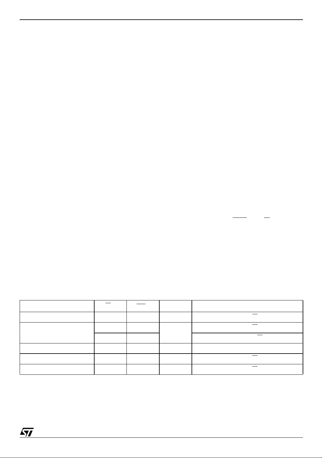
Figure 6. Setting the Write Protection Register (WC = 0)
BUS ACTIVITY
MASTER
SDA LINE
BUS ACTIVITY
CONTROL
START
BYTE
Setting the Software Write-Protection
The M34C02 has a hardware write-protection
feature, using the Write Control (WC
) signal. This
signal can be driven High or Low, and must be
held constant for the whole instruction sequence.
When Write Control (WC
) is held Low, the whole
memory array (addresses 00h to FFh) is write
protected. When W r ite Control (WC
) is held High,
the write protection of the memory array is
dependent on whether software write-protection
has been set.
Software write-protection allows the bottom half of
the memory area (addresses 00h to 7Fh) to be
permanently write protected irrespective of
subsequent states of the Write Control (WC
signal.
WORD
ADDRESS
ACK
VALUE
(DON'T CARE)
DATA
ACK
VALUE
(DON'T CARE)
STOP
ACK
AI01935B
The write protection feature is activated by writing
once to the Protection Register. The Protection
Register is accessed with the device select code
set to 0110b (as shown in Table 2), and the E2, E1
and E0 bits set according to the states being
applied on the E2, E1 and E0 signals. As for any
other write command, Write Control (WC
be held Low. Address and data bytes must be sent
with this command, but their values are all ignored,
and are treated as Don’t Care. Once the
Protection Register has been written, the write
protection of the first 12 8 bytes o f the memory is
enabled, and it is not pos sible to unprotect t hese
128 bytes, even if the device is powered off and
on, and regardless the state of Write Control (WC
)
When the Protection Register has been written,
the M34C02 no longer responds to the device type
identifier 0110b in either read or write mode.
) needs to
).
Figure 7. Result of Setting the Write Protection
FFh
80h
7Fh
00h
6/26
Memory
Area
Standard
Array
Standard
Array
Default EEPROM memory area
state before write access
to the Protect Register
Standard
Array
Write
Protected
Array
State of the EEPROM memory
area after write access
to the Protect Register
FFh
80h
7Fh
00h
AI01936C
Page 7
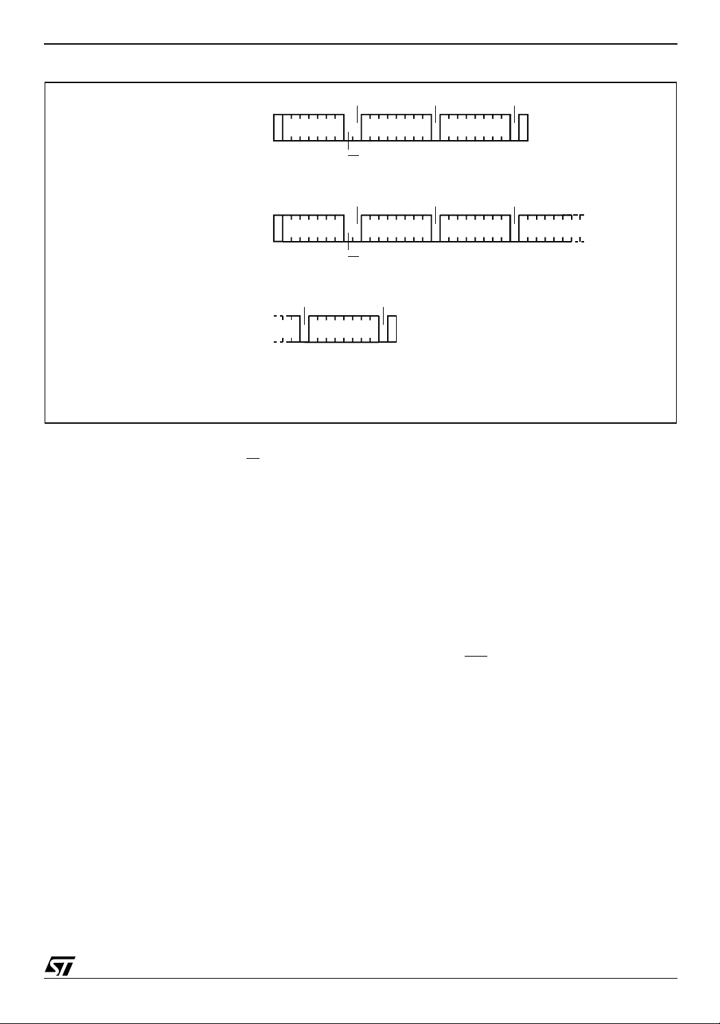
Figure 8. Write Mode Sequences in a Non Write-Protected Area
ACK ACK ACK
M34C02
BYTE WRITE DEV SEL BYTE ADDR
START
PAGE WRITE DEV SEL BYTE ADDR DATA IN 1 DATA IN 2
START
ACK ACK
DATA IN N
Write Operations
Following a Start condition the bus master sends
a Device Select Code with the RW
bit rese t to 0 .
The device acknowledges this, as shown in Figure
8, and waits f or an address byte. Th e device responds to the address byte with an acknowle dge
bit, and then waits for the data byte.
When the bus mast er generates a Stop con dition
immediately after the Ack bi t (in t he “10
th
bit” time
slot), either at the end of a Byte Write or a Page
Write, the internal memory Write cycle is triggered.
A Stop condition at any other time slot does not
trigger the internal Write cycle.
During the internal Write cycle, Serial Da ta (SDA)
and Serial Clock (SCL) are ignored, and the device does not respond to any requests.
Byte Write
After the Device Select Code and the address
byte, the bus mast er sends one data byte. If the
addressed location is hardware write-protected,
the device replies to the data byte with NoAck, and
the location is not modified. If, instead, the addressed location is not Write-protected, the device
DATA IN
R/W
ACK ACK ACK
R/W
STOP
STOP
AI01941
replies with Ack. The bus master terminates the
transfer by generating a Stop condition, as shown
in Figure 8.
Page Write
The Page Write mode allows u p to 16 by tes to be
written in a single Write cycle, provided that they
are all located in the same page in the memory:
that is, the most significant m emory address bits
are the same. If more bytes are sent than will fit up
to the end of the page, a condition known as ‘ r ollover’ occurs. This should be avoided, as data
starts to become overwritten in an implementation
dependent way.
The bus master sends fr om 1 to 16 bytes of data,
each of which is acknowledged by the device if
Write Control (WC
) is Low. If the addressed location is hardware write-protected, the device replies
to the data byte with NoAck, and the locations are
not modified. After each byte is transferred, the internal byte address counter (the 4 least significant
address bits only) is incremented. Th e transfer is
terminated by the bus master generating a Stop
condition.
7/26
Page 8
M34C02
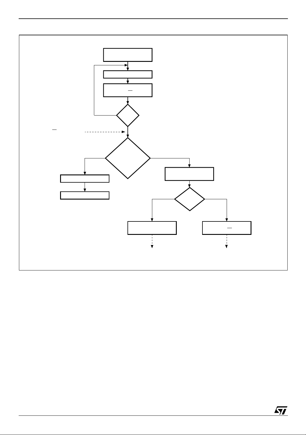
Figure 9. Wri te Cy cle Pol l in g Fl owchart using AC K
WRITE Cycle
in Progress
START Condition
DEVICE SELECT
with RW = 0
ACK
NO
Returned
First byte of instruction
with RW = 0 already
decoded by the device
ReSTART
STOP
YES
Next
Operation is
Addressing the
Memory
DATA for the
WRITE Operation
Continue the
WRITE Operation
Minimizing System Delays by Polling On ACK
During the internal Write cycle, the device disconnects itself from the bus, and writes a copy of the
data from its internal latches to the memory cells.
The maximum Write time (t
) is shown in Tables
w
16 and 17, but the typical time is shorter. To make
use of this, a polling sequence can be used by the
bus master.
The sequence, as shown in Figure 9, is:
– Initial condition: a Write cycle is in progress.
YESNO
Send Address
and Receive ACK
START
Condition
YESNO
DEVICE SELECT
with RW = 1
Continue the
Random READ Operation
AI01847C
– Step 1: the bus master issues a Start condition
followed by a Device Select Code (the first byte
of the new instruction).
– Step 2: if the device is busy with the internal
Write cycle, no Ack will be returned and the bus
master goes back to Step 1. If the device has
terminated the internal Write cycle, it responds
with an Ack, indicating that the device is ready
to receive the second part of the instruction (the
first byte of this instruction having been sent
during Step 1).
8/26
Page 9

Figure 10. Read Mode Sequences
M34C02
CURRENT ADDRESS READ
RANDOM ADDRESS READ
SEQUENTIAL
CURRENT
READ
SEQUENTIAL
RANDOM
READ
ACK
DEV SEL DATA OUT
R/W
START
ACK
DEV SEL * BYTE ADDR
R/W
START
ACK ACK ACK NO ACK
DEV SEL DATA OUT 1
R/W
START
ACK ACK
DEV SEL * BYTE ADDR
NO ACK
STOP
ACK ACK
DEV SEL * DATA OUT
START
DEV SEL * DATA OUT 1
NO ACK
R/W
DATA OUT N
ACK ACK
STOP
STOP
R/W
START
ACK NO ACK
DATA OUT N
STOP
Note: 1. The seven most sign i ficant bits of the D evice Select Code of a Random Read (in the 1st and 3rd bytes) must be identical.
Read Operations
Read operations are performed independently of
whether hardware or software protection has been
set.
The device has an internal address counter which
is incremented each time a byte is read.
Random Address Read
A dummy Write is first performed to load the address into this address c ounter (as shown in Figure 10) but
without
sending a Stop condition.
Then, the bus master sends another Start condition, and repeats the Device Select Code, with the
bit set to 1. The device acknowledges this,
RW
START
and outputs the contents of the addressed byte.
The bus master must
and terminates the transfer with a Stop condition.
Current Address Read
For the Current Address Read operation, following
a Start condition, the bus master only sends a Device Select Code with the RW
vice acknowledges this, and outputs the byte
addressed by the internal address counter. The
counter is then incremented. The bus master terminates the transfer with a Stop condition, as
shown in Figure 10,
byte.
R/W
AI01942
not
acknowledge the byte,
bit set to 1. The de-
without
acknowledging the
9/26
Page 10

M34C02
Sequenti a l Rea d
This operation can be used after a Current Address Read or a Random Address Read. The bus
master
does
acknowledge the data byte output,
and sends additional clock pulses so that the device continues to output the next byte in sequence.
To terminate the stream of bytes, the bus master
must
not
acknowledge the last byte, and
must
generate a Stop condition, as shown in Figure 10.
The output data comes from consecutive address-
es, with the internal address counter automatically
incremented after each byte output. After the last
memory address, the address counter ‘rolls-over’,
and the device continues to output data from
memory address 00h.
Acknowledge in Read Mode
For all Read commands, the device waits, after
each byte read, for an acknowledgment during the
th
bit time. If the bus master does not drive Serial
9
Data (SDA) Low during this time, the device terminates the data transfer and s witches to its St andby mode.
USE WITHIN A DRAM DIMM
In the application, the M34C02 is soldered directly
in the printed circuit modu le. The 3 Chip Enable
inputs (pins 1, 2 and 3) are wired at V
through the DIMM socket (s ee T able 4). The pullup resistors needed for normal behavior of the I
bus are connected on the I
2
C bus of the mother-
CC
or V
SS
2
board (as shown in Figure 11).
The Write Control (WC
unconnected. However, connecting it to V
) of the M34C02 can be left
is
SS
recommended, to maintain full read and write
access.
Programming the M34C02
When the M34C02 is delivered, full read and write
access is given to the whole memory array. It is
recommended that the first step is t o use the t est
equipment to write the module information (such
as its access speed, i ts size, its organization) to
the first half of the memory, starting from the first
memory location. When the data has been
validated, the test equipment can send a Write
command to the Protection Register, using the
device select code ’01100000b’ followed by an
address and data byte (made up of Don’t Care
values) as shown i n Figu re 6. Th e first 12 8 by tes
of the memory area are then write-protected, and
the M34C02 w ill no longer respond to the s pecif ic
device select code ’0110000xb’. It is not possible
to reverse this sequence.
Table 4. DRAM DIMM Connections
DIMM Position E2 E1 E0
V
0
1
2
3
4
5
6
VSS V
SS
V
VSS V
SS
V
VCC V
SS
V
VCC V
SS
V
VSS V
CC
V
VSS V
CC
V
VCC V
CC
C
V
7
VCC V
CC
INITIAL DELIVERY STATE
The device is delivered with the memory array
erased: all bits are set to 1 (each byte contains
FFh).
SS
CC
SS
CC
SS
CC
SS
CC
10/26
Page 11

Figure 11. Serial Presence Detect Block Diagram
M34C02
DIMM Position 7
DIMM Position 6
DIMM Position 5
DIMM Position 4
DIMM Position 3
V
CC
VCCV
V
CC
V
SS
R = 4.7kΩ
SDASCLE0E1E2
V
CC
SDASCLE0E1E2
V
SS
SDASCLE0E1E2
V
CC
SS
SDASCLE0E1E2
V
SS
SDASCLE0E1E2
V
CC
DIMM Position 2
VSSV
DIMM Position 1
V
SS
DIMM Position 0
AI01937
Note: 1. E0, E1 and E2 are wire d at e ach DIMM socket i n a bi nary sequenc e for a maximum of 8 devices.
2. Common clock and common data are shared acros s all the devices.
3. Pull-up resis to rs ar e requ ired on all S DA a nd SCL b us l ine s (typi call y 4. 7 kΩ) because t he se li nes ar e o pen dr ain w he n use d as
outputs.
V
SS
CC
V
CC
V
SS
SDASCLE0E1E2
SDASCLE0E1E2
SDASCLE0E1E2
SCL line SDA line
From the motherboard
2
I
C master controller
11/26
Page 12

M34C02
MAXI MUM RATING
Stressing the device ab ove the rating listed in the
Absolute Maximum Ratings" table may cause permanent damage to the device. These are stress
ratings only and operation of the device at these or
any other conditions ab ove those i ndicated in t he
Operating sections of this specificat ion is not im-
Table 5. Absolute Maximum Ratings
Symbol Parameter Min. Max. Unit
T
T
STG
LEAD
Storage Temperature –65 150 °C
Lead Temperature during
Soldering
PDIP: 10 seconds
SO: 20 seconds (max)
TSSOP: 20 seconds (max)
plied. Exposure to Absolute Maximum Rating conditions for extended periods may affect device
reliability. Refer also to the STMicroelectronics
SURE Program and ot her relevant quality documents.
1
1
260
235
235
°C
V
IO
V
CC
V
ESD
Note: 1. I PC/ JED EC J- STD- 02 0 A
2. JEDEC Std JESD 22-A114A (C1=100 pF, R1=1500 Ω, R2=500 Ω)
Input or Output range –0.6 6.5 V
Supply Voltage –0.3 6.5 V
Electrostatic Discharge Voltage (Human Body model)
2
–4000 4000 V
12/26
Page 13

DC AND AC PARAMETERS
This section summarizes the operat ing and measurement conditions, and the DC and AC characteristics of the device. The parameters in t he DC
and AC Characteristic tables that follow are derived from tests performed under the Measure-
ment Conditions summarized in the relevant
tables. Designers should chec k th at the o perat ing
conditions in their circuit matc h the meas urement
conditions when relying on the quoted parameters.
Table 6. Operating Conditions (M34C02-W)
Symbol Parameter Min. Max. Unit
M34C02
V
CC
T
A
Supply Voltage 2.5 5.5 V
Ambient Operating Temperature –40 8 5 °C
Table 7. Operating Conditions (M34C02-L)
Symbol Parameter Min. Max. Unit
V
CC
T
A
Supply Voltage 2.2 5.5 V
Ambient Operating Temperature –40 8 5 °C
Table 8. Operating Conditions (M34C02-R)
Symbol Parameter Min. Max. Unit
V
CC
T
A
Supply Voltage 1.8 5.5 V
Ambient Operating Temperature –40 8 5 °C
Table 9. Operating Conditions (M34C02-F)
Symbol Parameter Min. Max. Unit
V
CC
T
A
Supply Voltage 1.7 3.6 V
Ambient Operating Temperature 0 70 °C
13/26
Page 14

M34C02
Table 10. AC Measurement Conditions
Symbol Parameter Min. Max. Unit
C
L
Load Capacitance 100 pF
Input Rise and Fall Times 50 ns
Input Levels
Input and Output Timing Reference Levels
Figure 12. AC Measurement I/O Waveform
Input Levels
0.8V
CC
0.2V
CC
Table 11. Input Parameters
Symbol
C
IN
C
IN
Z
WCL
Z
WCH
t
NS
Note: 1. TA = 25 °C, f = 400 kHz
2. Sampled only, not 100% tested.
Input Capacitanc e (SDA) 8 pF
Input Capacitance (other pins) 6 pF
WC Input Impedance VIN < 0.5 V 5 20 k
WC Input Impedance
Pulse width ignored
(Input Filter on SCL and SDA)
Parameter
1,2
to 0.8V
0.2V
0.3V
Input and Output
Timing Reference Levels
0.7V
CC
0.3V
CC
AI00825B
CC
to 0.7V
CC
CC
CC
V
V
Test Condition Min. Max. Unit
Ω
V
> 0.7V
IN
CC
500 k
Ω
Single glitch 100 500 ns
14/26
Page 15

Table 12. DC Characteristics (M34C02-W)
Symbol Parameter
Input Leakage Current
I
LI
(SCL, SDA)
I
Output Leakage Current V
LO
I
CC
I
CC1
V
IL
V
IH
V
OL
Supply Current
Stand-by Supply Current
Input Low Voltage
(E2, E1, E0, SCL, SDA)
Input Low Voltage (WC
) –0.3
Input High Voltage
(E2, E1, E0, SCL, SDA, WC
Output Low Voltage
V
V
CC
)
Test Condition
(in addition to those in Table 6)
= VSS or V
V
IN
= VSS or V
OUT
=5V, fc=400kHz (rise/fall time < 30ns)
CC
CC
SDA in Hi-Z ± 2 µA
CC,
=2.5V , fc=400kHz (rise/fall time < 30ns)
= VSS or V
V
IN
V
= VSS or V
IN
= 3mA, VCC = 5V
I
OL
I
= 2.1mA, VCC = 2.5V 0.4 V
OL
CC
, V
CC
= 5V 1 µA
CC
, V
= 2.5V 0.5 µA
CC
Min.
–0.3 0.3V
0.7V
CC
M34C02
Max. Unit
± 2 µA
2mA
1mA
V
CC
0.5
VCC+1 V
0.4 V
V
Table 13. DC Characteristics (M34C02-L)
Symbol Parameter
Input Leakage Current
I
LI
(SCL, SDA)
Output Leakage Current V
I
LO
I
CC
I
CC1
V
IL
V
IH
V
OL
Supply Current
Stand-by Supply Current
Input Low Voltage
(E2, E1, E0, SCL, SDA)
Input Low Voltage (WC
) –0.3
Input High Voltage
(E2, E1, E0, SCL, SDA, WC
Output Low Voltage
V
V
)
(in addition to those in Table 7)
Test Condition
= VSS or V
V
IN
= VSS or V
OUT
V
=5V, fc=400kHz (rise/fall time < 30ns)
CC
=2.5V , fc=400kHz (rise/fall time < 30ns)
CC
=2.2V , fc=400kHz (rise/fall time < 30ns)
CC
= VSS or V
V
IN
V
= VSS or V
IN
CC
CC
SDA in Hi-Z ± 2 µA
CC,
, V
CC
= 5 V 1 µA
CC
, 2.2V ≤ VCC < 2.5V
Min.
–0.3 0.3V
0.7V
CC
= 3mA, VCC = 5V
I
OL
I
= 2.1mA, 2.2V ≤ VCC < 2.5V 0.4 V
OL
Max. Unit
± 2 µA
2mA
1mA
1mA
0.5 µA
V
CC
0.5
V
VCC+1 V
0.4 V
15/26
Page 16

M34C02
Table 14. DC Characteristics (M34C02-R)
Symbol Parameter
Input Leakage Curren t
I
LI
(SCL, SDA)
I
Output Leakage Current V
LO
I
CC
I
CC1
Supply Current
Stand-by Supply Current
V
CC
Test Condition
(in addition to those in Table 8)
= VSS or V
V
= VSS or V
OUT
IN
CC
SDA in Hi-Z ± 2 µA
CC,
=1.8V , fc=100kHz (rise/fall time < 30ns)
V
IN
V
= VSS or V
IN
= VSS or V
, V
CC
= 5V
CC
, 1.8V ≤ VCC < 2.5V 0.5 µA
CC
Min.
Max. Unit
± 2 µA
1mA
1µA
Input Low Voltage
V
V
V
(E2, E1, E0, SCL, SDA)
IL
Input Low Voltage (WC
Input High Voltage
IH
(E2, E1, E0, SCL, SDA, WC
Output Low Voltage
OL
) –0.3 0.5 V
)
Table 15. DC Characteristics (M34C02-F)
Symbol Parameter
Input Leakage Curren t
I
LI
(SCL, SDA)
I
Output Leakage Current
LO
I
I
Supply Current
CC
Stand-by Supply Current
CC1
Input Low Voltage
V
(E2, E1, E0, SCL, SDA)
IL
Input Low Voltage (WC
V
V
Note: 1. Preliminary Data.
Input High Voltage
IH
(E2, E1, E0, SCL, SDA, WC
Output Low Voltage
OL
) –0.3 0.5 V
V
CC
)
2.5V ≤ V
1.8V ≤ V
= 3mA, VCC = 5V 0.4 V
I
OL
I
= 2.1mA, 2.2V ≤ VCC < 2.5V
OL
= 0.15mA, VCC = 1.8V
I
OL
≤ 5.5V – 0.3
CC
< 2.5V – 0.3
CC
Test Condition
(in addition to those in Table 9)
= VSS or V
V
V
OUT
IN
= VSS or V
CC
SDA in Hi-Z
CC,
=1.7V , fc=100kHz (rise/fall time < 30ns)
= VSS or V
V
IN
V
= VSS or V
IN
2.5V ≤ V
1.7V ≤ V
= 2.1mA, 2.2V ≤ VCC ≤ 3.6V
I
OL
= 0.15mA, VCC = 1.7V
I
OL
, V
CC
, 1.7V ≤ VCC < 2.5V 0.5 µA
CC
CC
CC
= 3.6V 1 µA
CC
≤ 3.6V – 0.3
< 2.5V – 0.3
0.7V
Min.
0.7V
CC
1
CC
0.3 V
CC
0.25 V
CC
VCC+1
0.4 V
0.2
1
Max.
Unit
± 2 µA
± 2 µA
1mA
0.3 V
CC
0.25 V
CC
VCC+1 V
0.4 V
0.2
V
V
V
V
V
V
V
16/26
Page 17

Table 16. AC Characteristics (M34C02-W, M34C02-L)
Test conditions specified in Table 10 and Table 6 or 7
M34C02
Symbol Alt. Parameter
f
C
t
CHCL
t
CLCH
t
DL1DL2
t
DXCX
t
CLDX
t
CLQX
3
t
CLQV
1
t
CHDX
t
DLCL
t
CHDH
t
DHDL
t
W
Note: 1. For a reSTART condi ti on, or followi ng a Write cycle.
2. Sampled only, not 100% tested.
3. To avoid spurious START and STOP conditions, a minimum delay is placed between SCL=1 and the falling or rising edge of SDA.
f
SCL
t
HIGH
t
LOW
2
t
SU:DAT
t
HD:DAT
t
t
t
SU:STA
t
HD:STA
t
SU:STO
t
BUF
t
WR
Clock Frequency 400 kHz
Clock Pulse Width High 600 ns
Clock Pulse Width Low 1300 ns
t
SDA Fall Time 20 300 ns
F
Data In Set Up Time 100 ns
Data In Hold Time 0 ns
Data Out Hold Time 200 ns
DH
Clock Low to Next Data Valid (Access Time) 200 900 ns
AA
Start Condition Set Up Time 600 ns
Start Condition Hold Time 600 ns
Stop Condition Set Up Time 600 ns
Time between Stop Condition and Next Start Condition 1300 ns
Write Time 10 ms
Min. Max.
Table 17. AC Characteristics (M34C02-R, M34C02-F)
Test conditions specified in Table 10 and Table 8 or 9
Unit
Symbol Alt. Parameter
f
C
t
CHCL
t
CLCH
t
DL1DL2
t
DXCX
t
CLDX
t
CLQX
3
t
CLQV
1
t
CHDX
t
DLCL
t
CHDH
t
DHDL
t
W
Note: 1. For a reSTART condi ti on, or followi ng a Write cycle.
2. Sampled only, not 100% tested.
3. To avoid spurious START and STOP conditions, a minimum delay is placed between SCL=1 and the falling or rising edge of SDA.
f
SCL
t
HIGH
t
LOW
2
t
SU:DAT
t
HD:DAT
t
t
t
SU:STA
t
HD:STA
t
SU:STO
t
BUF
t
WR
Clock Frequency 100 kHz
Clock Pulse Width High 4000 ns
Clock Pulse Width Low 4700 ns
t
SDA Fall Time 20 300 ns
F
Data In Set Up Time 250 ns
Data In Hold Time 0 ns
Data Out Hold Time 200 ns
DH
Clock Low to Next Data Valid (Access Time) 200 3500 ns
AA
Start Condition Set Up Time 4700 ns
Start Condition Hold Time 4000 ns
Stop Condition Set Up Time 4000 ns
Time between Stop Condition and Next Start Condition 4700 ns
Write Time 10 ms
Min. Max.
Unit
17/26
Page 18

M34C02
Figure 13. AC Waveforms
SCL
SDA In
SCL
SDA In
SCL
tCHCL
tDLCL
tCHDX
START
Condition
tCHDH
STOP
Condition
tCLQV tCLQX
SDA
Input
tCLCH
SDA
Change
tW
Write Cycle
tDXCXtCLDX
tCHDH tDHDL
tCHDX
START
Condition
STOP
Condition
START
Condition
SDA Out
Data Valid
AI00795C
18/26
Page 19

PACKAGE MECHANICAL
PDIP8 – 8 pin Plastic DIP, 0.25mm lead frame, Package Outline
M34C02
b2
A2
A1AL
be
D
8
E1
1
Notes: 1. Drawing is not t o scale.
E
c
eA
eB
PDIP-B
PDIP8 – 8 pin Plastic DIP, 0.25mm lead frame, Package Mechanical Data
Symb.
Typ. Min. Max. Typ. Min. Max.
A 5.33 0.210
A1 0.38 0.015
mm inches
A2 3.30 2.92 4.95 0.130 0.115 0.195
b 0.46 0.36 0.56 0.018 0.014 0.022
b2 1.52 1.14 1.78 0.060 0.045 0.070
c 0.25 0.20 0.36 0.010 0.008 0.014
D 9.27 9.02 10.16 0.365 0.355 0.400
E 7.87 7.62 8.26 0.310 0.300 0.325
E1 6.35 6.10 7.11 0.250 0.240 0.280
e 2.54 – – 0.100 – –
eA 7.62 – – 0.300 – –
eB 10.92 0.430
L 3.30 2.92 3.81 0.130 0.115 0.150
19/26
Page 20

M34C02
SO8 narrow – 8 lead Plastic Small Outline, 150 mils body width, Package Ou tline
h x 45˚
Note: Drawing is not to scale.
B
SO-a
A
e
D
N
1
CP
E
H
C
LA1 α
SO8 narrow – 8 lead Plastic Small Outline, 150 mils body width, Package M echa nical Data
Symb.
Typ. Min. Max. Typ. Min. Max.
mm inches
20/26
A 1.35 1.75 0.053 0.069
A1 0.10 0.25 0.004 0.010
B 0.33 0.51 0.013 0.020
C 0.19 0.25 0.007 0.010
D 4.80 5.00 0.189 0.197
E 3.80 4.00 0.150 0.157
e 1.27 – – 0.050 – –
H 5.80 6.20 0.228 0.244
h 0.25 0.50 0.010 0.020
L 0.40 0.90 0.016 0.035
α
0° 8° 0° 8°
N8 8
CP 0.10 0.004
Page 21

M34C02
VFDFPN8 – 8 lead Very thin Fine pitch Dual Flat Package No lead 2x3mm², Package Outline
D2
Top View
8
726
E
1
A
A1
Note: 1. Drawing is not to scale.
2. The central pad (the area E2 by D2 in the above illust ration) is pulled, internall y, to V
any other volt age or signal lin e on the PCB, for example during the soldering process .
5
4
3
D
A3
L
E2
b
e
VFDFPN-02
. It must not be allowed to be connected to
SS
VFDFPN8 – 8 lead Very thin Fine pitch Dual Flat Package No lead 2x3mm², Package Mechanical
Data
Symbol
Typ. Min. Max. Typ. Min. Max.
A 0.90 0.80 1.00 0.035 0.031 0.039
A1 0.02 0.00 0.05 0.001 0.000 0.002
mm inches
A3 0.05 0.002
b 0.25 0.20 0.32 0.010 0.008 0.013
D 2.00 - - 0.079 - -
D2 1.65 1.50 1.75 0.065 0.059 0.069
E 3.00 - - 0.118 - -
E2 1.80 1.65 1.90 0.071 0.065 0.075
e 0.50 - - 0.020 - L 0.40 0.30 0.50 0.016 0.012 0.020
21/26
Page 22

M34C02
TSSOP8 – 8 lead Thin Shrink Small Outline, Package Outline
D
8
1
CP
Notes: 1. Drawing is not t o scale.
5
EE1
4
A2A
eb
A1
L1
TSSOP8 – 8 lead Thin Shrink Small Outline, Package Mec han ical Data
Symbol
Typ. M in. Max. Typ. Min. Max.
A 1.200 0.0472
A1 0.050 0. 150 0.0020 0.0059
A2 1.000 0.800 1. 050 0.0394 0.0315 0.0413
b 0. 190 0.300 0.0075 0.0118
c 0.090 0.200 0.0035 0.0079
mm inches
c
α
L
TSSOP8AM
22/26
CP 0.100 0.0 039
D 3.000 2.900 3.100 0.1181 0.1142 0.1220
e 0 .650 – – 0.0256 – –
E 6.400 6. 200 6.600 0.2520 0.2441 0.2598
E1 4.400 4.300 4. 500 0.1732 0.1 693 0.1772
L 0 .600 0.450 0.750 0.0236 0.0177 0.0295
L1 1.000 0.0 394
α
0° 8° 0° 8°
Page 23

TSSOP8 3x3mm² – 8 lead Thin Shrink Small Outline, 3x3mm² bo dy size , Packag e Outline
D
M34C02
8
1
CP
Notes: 1. Drawing is not t o scale.
5
EE1
4
A2A
A1
eb
L
L1
TSSOP8BM
c
α
TSSOP8 3x3mm² – 8 lead Thin Shrink Small Outline, 3x3mm² body size, Package Mechanical Data
Symbol
Typ. Min. Max. Typ. Min. Max.
A 1.100 0.0433
A1 0.050 0.150 0.0020 0.0059
A2 0.850 0.750 0.950 0.0335 0.0295 0.0374
b 0.250 0.400 0.0098 0.0157
c 0.130 0.230 0.0051 0.0091
mm inches
D 3.000 2.900 3.100 0.1181 0.1142 0.1220
E 4.900 4.650 5.150 0.1929 0.1831 0.2028
E1 3.000 2.900 3.100 0.1181 0.1142 0.1220
e 0.650 – – 0.0256 – –
CP 0.100 0.0039
L 0.550 0.400 0.700 0.0217 0.0157 0.0276
L1 0.950 0.0374
α
0° 6° 0° 6°
23/26
Page 24

M34C02
PART NUMBERING
Table 18. Ordering Information Scheme
Example2: M34C02 – W MN 6 T P
Device Type
M34 = ASSP I
Device Function
02 = 2 Kbit (256 x 8)
Operating Voltage
W = V
CC
L = V
CC
R = V
CC
F = V
CC
Package
1
= PDIP8
BN
MN = SO8 (150 mil width)
MM = VFDFPN8 (MLP8)
DW = TSSOP8 (169 mil width)
DS = TSSOP8 (3x3mm² body size, MSOP8)
2
C serial access EEPROM
= 2.5 to 5.5V (400kHz)
= 2.2 to 5.5V (400kHz)
= 1.8 to 5.5V (100kHz)
= 1.7 to 3.6V (100kHz)
Temperature Range
6 = –40 to 85 °C
1 = 0 to 70 °C
Option
T = Tape & Reel Packing
Plating Technology
2
blank = Standard SnPb plating
P = Pb-free plating
G = Green pack
Note: 1. Package availabl e only on request.
2. For a list of available options (speed, package, etc.) or for further information on any aspect of this device, please contact your nea rest ST Sales Offic e.
24/26
Page 25

REVISION HIST ORY
Table 19. Revision History
Date Rev. Description of Revision
27-Dec-1999 2.0
07-Dec-2000 2.1 New definition of lead soldering temperature absolute rating for certain packages
13-Mar-2001 2.2 -R voltage range added
18-Jul-2002 2.3 TSSOP8 (3x3mm² body size) package (MSOP8) added
22-May-2002 2.4 VFDFPN8 package (MLP8) added
21-Jul-2003 3.0 Document reformatted. -F voltage range added.
Adjustments to the formatting. 0 to 70°C temperature range removed from DC and AC tables.
No change to description of device, or parameters
M34C02
25/26
Page 26

M34C02
Information furnished is bel i eved to be accurate an d rel i able. However, STMicroelectronics assumes no responsibility for the consequences
of use of such information nor for any infringement of patents or other rights of third parties which may result from its use. No license is granted
by implic ation or otherwise under any patent or patent rights of STMicroel ectronics. Sp ecifications mentioned in this publicati on are subject
to change without notice. This publication supersedes and replaces all information previously supplied. STMicroelectronics products are not
authorized for use as criti cal components in l i fe support devices or systems wit hout express written approval of STM i croelectronics.
The ST log o i s registered tr ademark of STMic roelectroni cs
All other nam es are the prope rty of their respec tive owners
© 2003 STMicroelectronics - All Rights Reserved
STMicroelectronics group of companies
Austra lia - Brazil - Canada - Chi na - Finland - Fr ance - Germany - Hong Kong -
India - Israel - Italy - Japan - Malaysia - Mal ta - Morocco - Singapore - Spain - S weden - Switzer l and - United Kin gdom - United States.
www.st.com
26/26
 Loading...