

Page 1
1/15
PRODUCT PREVIEW
April 2001
This is preliminary information on a new product now in development. Details are subject to change without notice.
M34A02
2 Kbit Serial SMBus EEPROM for ACR Card Configuration
■ Two Wire SMBus Serial Interf a ce
■ 2.7V to 3.6V Single Supply Voltage
■ Hardware Write Control
■ BYTE and PAGE WRITE (up to 16 Bytes)
■ RANDOM and SEQUENTIAL READ Modes
■ Self-Tim ed P ro g ra m ming Cycle
■ Automatic Address Incrementing
■ Enhanced ESD/Latch-Up Behavior
■ More than 1 Million Erase/Write Cycles
■ More than 40 Year Data Retention
DESCRIPTION
These electrically erasable programmable
memory (EEPROM) devices are organized as
256x8 bits, and operate down to 2.7 V.
These devices are available in Plastic Small
Outline and Thin Shrink Small Outline packages.
These devices are written by the ACR card-issuer,
and then accessed in Read mode in the
application, using the ACR Serial Bus protocol.
This is a two wire serial interface that uses a bidirectional data bus and serial clock. The device
carries a built-in 4-bit Device Type Identifier code
(1011).
The device behaves as a slave i n the ACR Serial
Bus protocol, with all memory operations
synchronized by the serial clock. Read and Write
operations are initiated by a Start condition,
generated by the bus master. Th e Start con dition
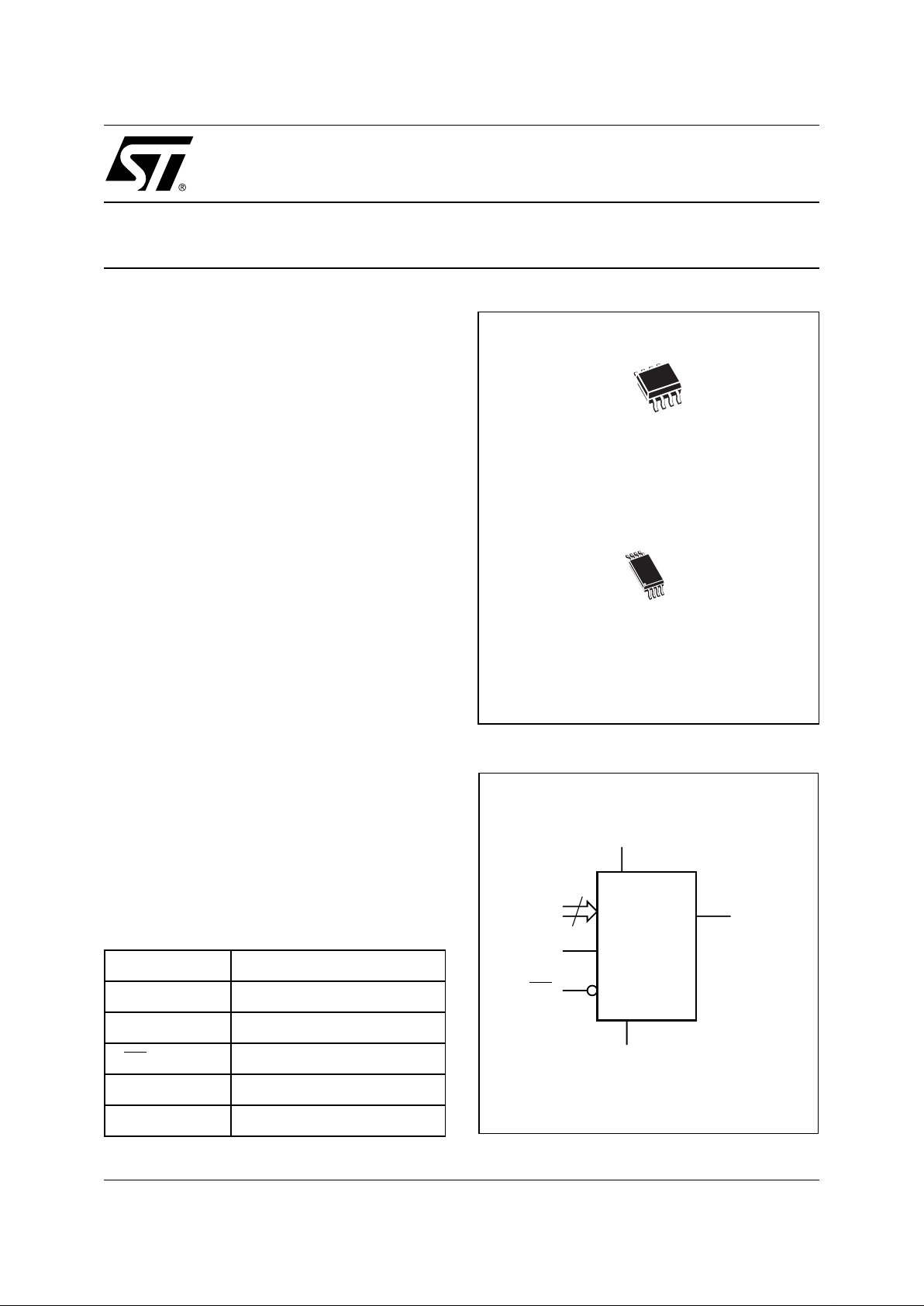
Figure 1. Logic Diagram
AI03794
SDA
V
CC
M34A02
WC
SCL
V
SS
3
E0-E2
Table 1. Signal Names
E0, E1, E2 Chip Enable
SDA Serial Data
SCL Serial Clock
WC
Write Control
V
CC
Supply Voltage
V
SS
Ground
SO8 (MN)
150 mil width
TSSOP8 (DW)
169 mil width
8
1
8
1
Page 2
M34A02
2/15
is followed by a Device Select code and RW bit (as
described in Table 3), terminated by an
acknowledge bit.
When writing data to the memory, the device
inserts an acknowledge bit during the 9
th
bit time,
following the bus master’s 8-bit transmission.
When data is read by the bus master, the bus
master acknowledges the receipt of the data byte
in the same way. Data transfers are terminated by
a Stop condition after an Ack for Write, and after a
NoAck for Read.
Power On Reset: V
CC
Lock-Out Write Protect
In order to prevent data corruption and inadvertent
Write operations during Power-up, a Power On
Reset (POR) circuit is included. The internal reset
is held active until V
CC
has reached the POR
threshold value, and all operations are disabled –
the device will not respond to any command. In the
same way, when V
CC
drops from the operating
voltage, below the POR threshold value, all
operations are disabled and the device will not
respond to any com ma nd. A s table a nd v alid V
CC
must be applied before applying any logic signal.
SIGNAL DESCRIPTION
Serial Clock (SCL)
This input signal is use d to strobe all data in and
out of the device. In applications where this line is
used by slave devices to synchronize the bus to a
slower clock, the bus master must have an open
drain output, and a pull-up resistor must be
connected from Serial Clock (SCL) to V
CC
. (Figure
3 indicates how t he value of the pull-up resistor
Figure 2. SO and TSSOP Connections
1
AI03795
2
3
4
8
7
6
5
SDAV
SS
SCL
WCE1
E0 V
CC
E2
M34A02
Table 2. Absolute Maximum Ratings
1
Note: 1. Exc ept for the rating “Operating Temperature Ra nge”, stres ses above those listed in the Table “Absolute Maximum Ratings” may
cause permanent damage to the device. These are stress ratings only, and operation of the device at these or any other conditions
above those indicated in the Operating sections of this specification is not implied. Exposure to Absolute Maximum Rating
conditions for extended periods may affect device reliability. Refer also to the ST SURE Program and other relevant quality
document s.
2. IPC/ JEDEC J-STD- 020A
3. JED EC St d JESD22-A 114A (C1=1 00 pF, R1=1500 Ω, R2=500 Ω)
Symbol Parameter Value Unit
T
A
Ambient Operating Temperature –40 to 125 °C
T
STG
Storage Temperature –65 to 150 °C
T
LEAD
Lead Temperature during
Soldering
SO8: 20 seconds (max)
2
TSSOP8: 20 seconds (max)
2
235
235
°C
V
IO
Input or Output range –0.6 to 6.5 V
V
CC
Supply Voltage –0.3 to 6.5 V
V
ESD
Electrostatic Discharge Voltage (Human Body model)
3
4000 V
Figure 3. Typical ACR Application PCB
Connection (showing E2,E1,E0 address 000)
Note: 1. This arrangement on the chip enable lines allows the
application to start at ACR addres s 000h.
AI04092
E0
E1
E2
V
SS
V
CC
WC
SCL
SDA
V
CC
V
SS
ACR Bus
R
L
Page 3
3/15
M34A02
can be calculated). In most applications, t hough,
this method of synchronization is not employed,
and so the pull-up resistor is not necessary,
provided that the bus master has a push-pull
(rather than open drain) output.
Serial Data (SDA)
This bi-directional signal is used to transfer data in
or out of the device. It is an open drain output that
may be wire-OR’ed with other open drain or open
collector signals on the bus. A pull up resistor must
be connected from Serial Data (SDA) to V
CC
.
(Figure 3 indicates how the value of the pull-up
resistor can be calculated).
Chip Enable (E0, E1, E2)
These input signals are used to set the value that
is to be looked for on the three least significant bits
(b3, b2, b1) of the 7-bit Device Select Code. These
inputs should be tied t o V
CC
or VSS, to estab lish
the Device Select Code.
Write Control (WC
)
This input signal is useful for protecting the entire
contents of the memory from inadvertent erase
and write operations. Write operations are
disabled to the entire mem ory array when Write
Control (WC
) is held High. When unconnected, the
signal is internally read as V
IL
, and Write
operations are allowed.
When Write Control (WC
) is held High, Device
Select and Address bytes are acknowledged,
Data bytes are
not
acknowledged.
DEVICE OPERATION
The device supports the ACR Serial Bus protocol.
This is summarized in Figure 4. Any device that
sends data on to the bus is defined to be a
transmitter, and any device that reads the data to
be a receiver. The device that controls the data
transfer is known as the bus master, and the other
as the slave device. A data tran sfer can only be
initiated by the bus master, which will also provide
the serial clock for synchronization. The device is
always a slave in all communication.
Start Condition
Start is identified by a falling edge of Serial Data
(SDA) while Serial Clock (SCL) is stable in the
High state. A Start condition must precede any
data transfer command. The de vice continuously
monitors (except duri ng a Write cycle ) Se ri a l Data
(SDA) and Serial Clock (SCL) for a Start condition,
and will not respond unless one is give n.
Stop Condition
Stop is identified by a rising edg e of the SDA l ine
while the clock SCL is stable in the High state. A
Stop condition terminates communication
between the device and the bus master. A Stop
condition at the end of a Read command, provided
that it is followed by NoAck, forces the device into
its Stand-by mode. A Stop condition at the end of
a Write command triggers the internal EEPROM
Write cycle.
Acknowledge Bit (ACK)
The acknowledge bit is used to indicate a
successful byte transfer. The bus transmitter,
whether it be bus master or slave device, releases
Serial Data (SDA) after sending eight bits of data.
During the 9
th
clock pulse period, the receiver pulls
Serial Data (SDA) Low to acknowledge the receipt
of the eight data bits.
Data Input
During data input, the device samples Serial Data
(SDA) on the rising edge of Serial Clock (SCL).
Figure 4. Maximum R
L
Value versus Bus Capacitance (C
BUS
) for an ACR Serial Bus
AI01665
V
CC
C
BUS
SDA
R
L
MASTER
R
L
SCL
C
BUS
100
0
4
8
12
16
20
C
BUS
(pF)
Maximum RP value (kΩ)
10 1000
fc = 400kHz
fc = 100kHz
Page 4
M34A02
4/15
For correct device operation, Serial Data (SDA)
must be stable before the rising edge of Serial
Clock (SCL), and the data must change
only
after
Serial Clock (SCL) is Low.
Memory Addressing
To start communication betwee n the bus master
and the slave device, the bus mas ter mus t initiate
a Start condition. Following this, t he bus master
sends the 8-bit byte, shown in Table 3, on Serial
Data (SDA) (most significant bit first). This
consists of the 7-bit Device Select code, and the
Read/Write
bit (RW).
The Device Select Code consists of a 4-bit Device
Type Identifier, and a 3-bit Chip Enable “Address”
(E2, E1, E0). To address the memory array, t he 4bit Device Type Identifier is 1011b.
Up to eight memory devices can be connected on
a single bus. Each one is given a unique 3-bit code
on Chip Enable (E0, E1, E2). When the Device
Select Code is received on Serial Data (SDA), the
device only responds if the Chip Select Code is the
Figure 5. ACR Serial Bus Protocol
SCL
SDA
SCL
SDA
SDA
START
Condition
SDA
Input
SDA
Change
AI00792B
STOP
Condition
1 23 789
MSB
ACK
START
Condition
SCL
1 23 789
MSB ACK
STOP
Condition
Table 3. Device Select Code
1
Note: 1. The most significant bit, b7, is sent firs t.
Device Type Identifier Chip Enable RW
b7 b6 b5 b4 b3 b2 b1 b0
Device Select Code 1 0 1 1 E2 E1 E0 RW
Page 5
5/15
M34A02
same as the pattern applied on Chip Enable (E0,
E1, E2 ) .
The 8
th
bit is the Read/Write bit (RW). This bit is
set to 1 for Read and 0 for Write operations. If a
match occurs on the Device Select code, the
corresponding device gives an acknowledgment
on Serial Data (SDA) during the 9
th
bit time. If the
device does not match the Device Select code, it
deselects itself from the bus, and goes into Standby mode.
Table 4. Operating Modes
Note: 1. X = V
IH
or V
IL
.
Mode RW bit
WC
1
Bytes Initial Sequence
Current Address Read 1 X 1 START, Device Select, RW
= 1
Random Address Read
0X
1
START, Device Select, RW
= 0, Address
1 X reSTART, Device Select, RW
= 1
Sequential Read 1 X
≥
1 Similar to Current or Random Address Read
Byte Write 0
V
IL
1 START, Device Select, RW = 0
Page Write 0
V
IL
≤
16 START, Device Select, RW
= 0
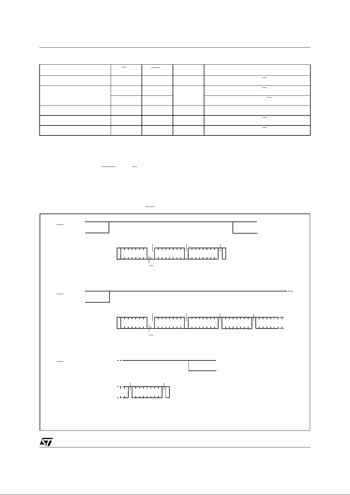
Figure 6. Wri te Mo de S e qu e nces with WC =1 (data wri te inhibi ted)
STOP
START
Byte Write DEV SEL BYTE ADDR DATA IN
WC
START
Page Write DEV SEL BYTE ADDR DATA IN 1 DATA IN 2
WC
DATA IN 3
AI02803C
Page Write
(cont'd)
WC (cont'd)
STOP
DATA IN N
ACK ACK NO ACK
R/W
ACK ACK NO ACK NO ACK
R/W
NO ACK NO ACK
Page 6

M34A02
6/15
Figure 7. Wri te Mo de S e qu e nces with WC =0 (data wri te enab led)
STOP
START
BYTE WRITE DEV SEL BYTE ADDR DATA IN
WC
START
PAGE WRITE DEV SEL BYTE ADDR DATA IN 1 DATA IN 2
WC
DATA IN 3
AI02804
PAGE WRITE
(cont'd)
WC (cont'd)
STOP
DATA IN N
ACK
R/W
ACK ACK
ACK ACK ACK ACK
R/W
ACKACK
Write Operations
Following a Start condition the bus master sends
a Device Select code with the R W
bit reset to 0.
The device acknowledges this, as shown in Figure
6, and waits for one address byte. The device
responds to the address byte with an acknowledge
bit, and then waits for the data byte.
Writing to the memory may be inhibited if Write
Control (WC
) is taken High. Any Write instruction
with Write Control (WC
) held High (during a period
of time from the Start condition until the end of the
address byte) will not modify the memory
contents, and the accompanying data bytes are
not
acknowledged, as shown in Figure 5.
Eac h dat a by t e i n th e me mo ry has a 8- bi t a dd re s s .
When the bus mast er generates a Stop con dition
immediately after the Ack bi t (in t he “10
th
bit” time
slot), either at the end of a Byte Write or a Page
Write, the internal memory Write cycle is triggered.
A Stop condition at any other time does not trigger
the internal Write cycle.
During the internal Write cycle, Serial Da ta (SDA)
is disabled internally, and the device does not
respond to any requests (and sends NoAck in
reply to them).
Byte Write
After the Device Select code and the address byte,
the bus master sends one data byte. If the
addressed location is Write-protected, by Write
Control (WC
), the device replies with NoA ck, and
the location is not modified. If, instead, the
addressed location is not Write-protected, the
device replies with Ack. The bus master
terminates the transfer by generating a Stop
condition, as shown in Figure 6.
Page Write
The Page Write mode allows u p to 16 by tes to be
written in a single write cycle, provided that they
are all located in the same ’row’ in the memory:
that is the most significant memory add ress bits
(b7-b4) are the same. I f m ore byt es are sent than
will fit up to t he en d of t he row, a condition known
Page 7

7/15
M34A02
as ‘roll-over’ occurs. Data starts to become
overwritten (in a way not formally specified in this
data sheet).
The bus master sends fr om one up to 16 bytes of
data, each of which is acknowledged by the
memory if Write Control (WC
) is Low. If Write
Control (WC
) is High, the contents of the
addressed memory location are not modified, and
each data byte is followed by a NoAck. After each
byte is transferred, the internal byte address
counter (the 4 least significant bits only) is
incremented. The transfer is terminated by the bus
master generating a Stop condition.
Minimizing System Delays by Polling On ACK
During the internal Write cycle, the device
disconnects itself from the bus, and copies the
data from its internal latches to the memory cells.
The ma x imum Write time ( t
w
) is shown in Table 6,
but the typical time is shorter. To make use of this,
an Ack polling sequenc e can be used by t he bus
master.
The sequence, as shown in Figure 7, is:
– Initial condition: a Write cycle is in progress.
– Step 1: the bus master issues a Start condition
followed by a D evice S ele ct code (the first byte
of the new instruction).
– Step 2: if the device is busy with the internal
Write cycle, no Ack will be returned and the bus
master goes back to Step 1. If the device has
terminated the internal Write cycle, it responds
with an Ack, indicating that the memory is ready
to receive the second part of the next instruction
(the first byte of this instruction having been sent
during Step 1).
Read Operations
Read operations are performed independently of
the state of the Write Control (WC
) signal.
Figure 8. Wri te Cy cle Pol l in g Fl owchart usin g A C K
WRITE Cycle
in Progress
AI01847C
Next
Operation is
Addressing the
Memory
START Condition
DEVICE SELECT
with RW = 0
ACK
Returned
YES
NO
YESNO
ReSTART
STOP
DATA for the
WRITE Operation
DEVICE SELECT
with RW = 1
Send Address
and Receive ACK
First byte of instruction
with RW = 0 already
decoded by the device
YESNO
START
Condition
Continue the
WRITE Operation
Continue the
Random READ Operation
Page 8

M34A02
8/15
Figure 9. Read Mode Sequences
Note: 1. The seven most significan t bits of the Dev i ce Select Co de of a Random Read (in the 1st and 3rd bytes) must be identic al .
START
DEV SEL * BYTE ADDR
START
DEV SEL DATA OUT 1
AI01942
DATA OUT N
STOP
START
CURRENT
ADDRESS
READ
DEV SEL DATA OUT
RANDOM
ADDRESS
READ
STOP
START
DEV SEL * DATA OUT
SEQUENTIAL
CURRENT
READ
STOP
DATA OUT N
START
DEV SEL * BYTE ADDR
SEQUENTIAL
RANDOM
READ
START
DEV SEL * DATA OUT 1
STOP
ACK
R/W
NO ACK
ACK
R/W
ACK ACK
R/W
ACK ACK ACK NO ACK
R/W
NO ACK
ACK ACK
R/W
ACK ACK
R/W
ACK NO ACK
Current Address Read operation, following a Start
condition, the bus master only sends a Device
Select Code with the RW
bit set to 1. The device
acknowledges this, and outputs the byte
addressed by the internal address counter. The
counter is then incremented. The bus master
terminates the transfer with a Stop condition, as
shown in Figure 8,
without
acknowledging the
byte.
Sequenti a l Rea d
This operation can be used after a Current
Address Read or a Random Address Read. The
bus master
does
acknowledge the data byte
Random Address Read
A dummy Write is performed to load the address
into the address counter (as shown in Figure 8) but
without
sending a Stop condition. Then, t he bus
master sends another Start condition, and repeats
the Device Select Code, with t he RW
bit set to 1.
The device acknowledges this, and outputs the
contents of the addressed byte. The bus master
must
not
acknowledge the byte, and terminates
the transfer with a Stop condition.
Current Address Read
The device has an internal address counter which
is incremented each time a byte is read. For the
Page 9

9/15
M34A02
Table 5. DC Characteristics
(T
A
= –40 to 85 °C; VCC = 2.7 to 3.6 V)
Table 6. AC Characteristics
Note: 1. For a r eS tart condit i on, or follo wi ng a Write cyc l e.
2. Samp l ed only, not 100% tes ted.
3. To avoid spurious Start and Stop conditions, a minimum delay is placed between SCL=1 and the falling or rising edge of SDA.
Symbol Parameter Test Condition Min. Max. Unit
I
LI
Input Leakage Current
(SCL, SDA, E2, E1, E0)
0V ≤ V
IN
≤ V
CC
± 2 µA
I
LO
Output Leakage Current 0 V ≤ V
OUT
≤ V
CC,
SDA in Hi-Z ± 2 µA
I
CC
Supply Current
V
CC
=3.6V, fc=100kHz (rise/fall time < 30ns)
2mA
V
CC
=2.7V, fc=100kHz (rise/fall time < 30ns)
1mA
I
CC1
Supply Current (Stand-by)
V
IN
= VSS or V
CC
1µA
V
IL
Input Low Voltage
(E0-E2, SCL, SDA)
– 0.3 0.8 V
V
IH
Input High Voltage
(E0-E2, SCL, SDA)
2.1 V
CC
+1 V
V
IL
Input Low Voltage (WC) – 0.3 0.5 V
V
IH
Input High Voltage (WC) 2.1 VCC+1 V
V
OL
Output Low Voltage IOL = 3 mA 0.4 V
Symbol Alt. Parameter
M34A02
Unit
V
CC
=2.7 to 3.6V
T
A
= –40 to 85°C
Min Max
t
CH1CH2
t
R
Clock Rise Time 1000 ns
t
CL1CL2
t
F
Clock Fall Time 300 ns
t
DH1DH2
2
t
R
SDA Rise Time 1000 ns
t
DL1DL2
2
t
F
SDA Fall Time 300 ns
t
CHCL
t
HIGH
Clock Pulse Width High 4 µs
t
CLCH
t
LOW
Clock Pulse Width Low 4.7 µs
t
CHDX
1
t
SU:STA
START Set-up Time 4.7 µs
t
DLCL
t
HD:STA
START Hold Time 4 µs
t
DXCX
t
SU:DAT
SDA In Set-up Time 250 ns
t
CLDX
t
HD:DAT
SDA In Hold Time 0 µs
t
CHDH
t
SU:STO
STOP Set-up Time 4 µs
t
DHDL
t
BUF
Time the bus must be free between STOP and next START 4.7 µs
t
CLQV
3
t
AA
Clock Low to SDA Out Valid 400 900 ns
t
CLQX
t
DH
SDA Out Hold Time after Clock Low 300 ns
f
C
f
SCL
Clock Frequency 10 100 kHz
t
W
t
WR
Write Time 10 ms
Page 10

M34A02
10/15
Table 7. Input Parameters1 (TA = 25 °C, f = 100 kHz)
Note: 1. Sampled only, not 100% tested.
Symbol Parameter Test Condition Min. Max. Unit
C
IN
Input Capacitance (SDA) 8 pF
C
IN
Input Capacitance (other pins) 6 pF
Z
WCL
WC Input Impedance VIN < 0.5 V 5 70 k
Ω
Z
WCH
WC Input Impedance VIN > 0.7V
CC
500 k
Ω
t
NS
Pulse width ignored
(Input Filter on SCL and SDA)
Single glitch 100 ns
Figure 10. AC Measurement Conditions
AI03799
2.3V
0.4V
2.1V
0.8V
Input Rise and Fall Times
<= 50 ns
Input Pulse Voltages
0.4V to 2.3V
Input and Output Timing
Reference Voltages
0.8V to 2.1V
Figure 11. AC Waveforms
SCL
SDA In
SCL
SDA Out
SCL
SDA In
tCHCL
tDLCL
tCHDX
START
Condition
tCLCH
tDXCXtCLDX
SDA
Input
SDA
Change
tCHDH tDHDL
STOP
Condition
Data Valid
tCLQV tCLQX
tCHDH
STOP
Condition
tCHDX
START
Condition
Write Cycle
tW
AI00795C
START
Condition
Page 11

11/15
M34A02
Table 8. Ordering Information Scheme
Example: M34A02 – V DW 6 T
Memory Capacity Option
02 2 Kbit (256 x 8) T Tape and Reel Packing
Operating Voltage
V 2.7 V to 3.6 V
Package Temperature Range
MN SO8 (150 mil width) 6 –40 °C to 85 °C
DW TSSOP8 (169 mil width)
output, and sends additional clock pulses s o that
the device continues to output the next byte in
sequence. To terminate the strea m of bytes, the
bus master must
not
acknowledge the last byte,
and
must
generate a Stop condition, as shown in
Figure 8.
The output data comes from consecutive
addresses, with the internal address counter
automatically incremen ted af t er ea ch byt e out put.
After the last memory address, the address
counter ‘rolls-over’, and the device continues to
output data from memory address 00h.
Acknowledge in Read Mode
For all Read commands, the device waits, after
each byte read, for an acknowledgment during the
9
th
bit time. If the bus master does not drive Serial
Data (SDA) Low during this time, the device
terminates the data transfer and switches to its
Stand-by mode.
ORDERING INFORMATION
Devices are shipped from the factory with the
memory content set at all 1s (FFh).
The notation used for the device number is as
shown in Table 8. For a list of a vai lable options
(speed, package, etc.) or for further information on
any aspect of this device, please contact your
nearest ST Sales Office.
Page 12

M34A02
12/15
SO8 narrow – 8 lead Plastic Small Outline, 150 mils body width
Note: Drawing is not to scale.
SO-a
E
N
CP
B
e
A
D
C
LA1 α
1
H
h x 45˚
SO8 narrow – 8 lead Plastic Small Outline, 150 mils body width
Symb.
mm inches
Typ. Min. M ax. Typ. Min. Ma x.
A 1.35 1.75 0.053 0.069
A1 0.10 0.25 0.004 0.010
B 0.33 0.51 0.013 0.020
C 0.19 0.25 0.007 0.010
D 4.80 5.00 0.189 0.197
E 3.80 4.00 0.150 0.157
e 1.27 – – 0.050 – –
H 5.80 6.20 0.228 0.244
h 0 .25 0.50 0.0 10 0.020
L 0 .40 0.90 0.0 16 0.035
α
0° 8° 0° 8°
N8 8
CP 0.10 0.004
Page 13

13/15
M34A02
TSSOP8 – 8 lead Thin Shrink Small Outline
Note: 1. Drawing is not to scale.
TSSOP
1
N
CP
N/2
DIE
C
L
A1
EE1
D
A2A
α
eB
TSSOP8 – 8 lead Thin Shrink Small Outline
Symb.
mm inches
Typ. Min. M ax. Typ. Min. Ma x.
A 1.10 0.043
A1 0.05 0.15 0.002 0.006
A2 0.85 0.95 0.033 0.037
B 0.19 0.30 0.007 0.012
C 0.09 0.20 0.004 0.008
D 2.90 3.10 0.114 0.122
E 6.25 6.50 0.246 0.256
E1 4.30 4.50 0.169 0.177
e 0.65 – – 0.026 – –
L 0 .50 0.70 0.0 20 0.028
α
0° 8° 0° 8°
N8 8
CP 0.08 0.003
Page 14

M34A02
14/15
Table 9. Revision History
Date Rev. Description of Revision
19-Sep-2000 1.0 Document written
14-Mar-2001 1.1
Lead Soldering Temperature in the Absolute Maximum Ratings table amended
Write Cycle Polling Flow Chart using ACK illustration updated
20-Apr-2001 1.2
References to I
2
C changed to ACR Serial Bus
Page 15

15/15
M34A02
Information furnished is believed to be accurate and reliable. However, STMicroelectronics assumes no responsibility for the consequences
of use of such information nor for any infringement of patents or other rights of third parties which may result from its use. No license is granted
by implic ation or otherwise under any patent or p atent rights of STMi croelectr oni cs. Spec i fications mentioned i n this publicatio n are subject
to change without notice. This publication supersedes and replaces all information previously supplied. STMicroelectronics products are not
authorized for use as cri tical comp onents in life support dev i ces or systems wi t hout expres s written approval of STMi croelectr o nics.
The ST logo is registered trademark of STMicroelectronics
All other names are the propert y of their respective owners
© 2001 STMicroelectronics - All Rights Reserved
STMicroelectronics GROUP OF COMPANIES
Australi a - Brazil - Ch i na - Finland - Fr ance - Germa n y - Hong Kong - India - Italy - J apan - Malays ia - Malta - Morocco -
Singap ore - Spain - Sweden - Swit zerland - Uni ted Kingdom - U.S.A.
www.st.com
 Loading...