

Page 1
256x 256 DIGITALSWITCHING MATRIX
.256 INPUT AND 256 OUTPUT CHANNEL
CMOS DIGITAL SWITCHING MATRIX COMPATIBLEWITHM088
.BUILDING BLOCK DESIGNED FOR LARGE
CAPACITYELECTRONICEXCHANGES,SUBSYSTEMSAND PABX
.NO EXTRA PIN NEEDED FOR NOT-BLOCK-
INGSINGLESTAGEAND HIGHERCAPACITY
SYNTHESIS BLOCKS(512 or 1024 channels)
.EUROPEAN TELEPHONE STANDARD COM-
PATIBLE(32serialchannelsperframe)
.PCM INPUTS AND OUTPUTS MUTUALLY
COMPATIBLE
.ACTUAL INPUT-OUTPUT CHANNEL CON-
NECTIONS STORED AND MODIFIED VIA AN
ON CHIP 8-BIT PARALLEL MICROPROCESSORINTERFACE
.TYPICALBITRATE : 2Mbit/s
.TYPICAL SYNCHRONIZATION RATE : 8KHz
(timeframe is 125µs)
.5VP0WER SUPPLY
.CMOS & TTL INPUT/OUTPUT LEVELS COM-
PATIBLE
.HIGH DENSITY ADVANCED 1.2µmHCMOS3
PROCESS
M3488
PRELIMINARY DATA
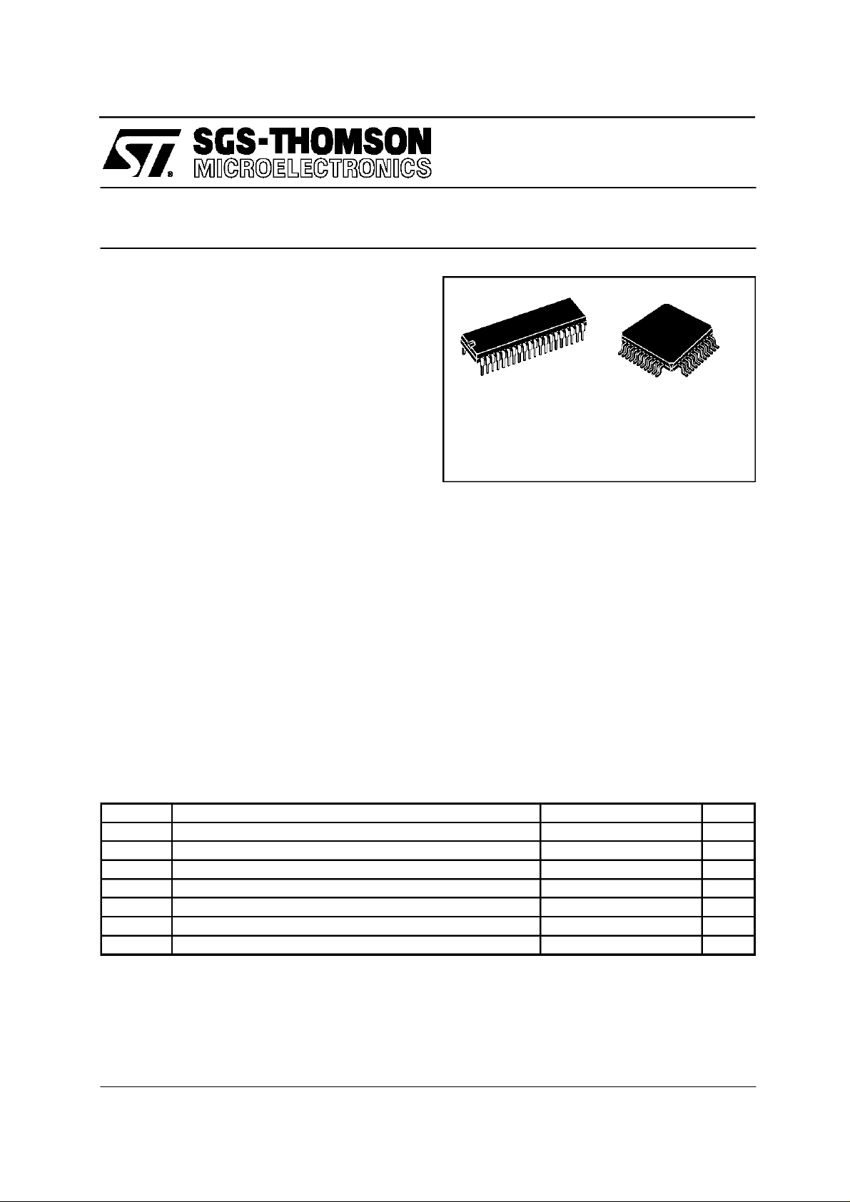
DIP40 PQFP44
ORDERING NUMBERS:
M3488B1 M3488Q1
Main instructionscontrolledby the microprocessor interface
.CHANNELCONNECTION/DISCONNECTION
.OUTPUT CHANNEL DISCONNECTION
.INSERTION OF A BYTE ON A PCM OUTPUT
CHANNEL/DISCONNECTION
.TRANSFERTO THE MICROPROCESSOROF
A SINGLEPCM OUTPUT CHANNELSAMPLE
.TRANSFERTO THE MICROPROCESSOROF
A SINGLE OUTPUT CHANNEL CONTROL
WORD
.TRANSFERTO THE MICROPROCESSOROF
A SELECTED0CHANNEL PCM INPUT DATA
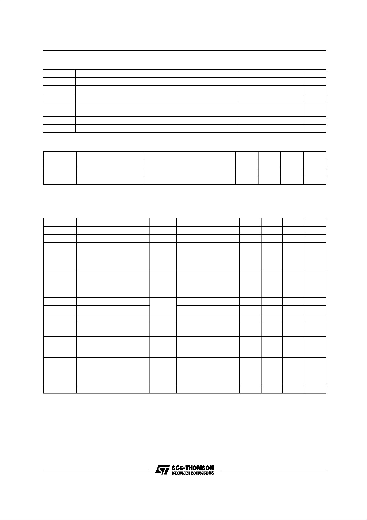
ABSOLUTE MAXI M UM RATI NG S
Symbol Parameter Test Conditions Unit
V
CC
V
V
I
O
P
T
stg
T
Str esses above t hose li st ed under ” Absolute Maximum Rati ngs” may cause per manent damage to the devi ce. This is a st r ess
rati ngs only and funct i onal operati on of the device at these or any other c ondit i ons above t hose ind icated in the operat i ng condition s of this specifi cation is not i mplied. Exposure to absolute maximum rati n g conditions for extended periods may affect device
reliability.
November 1994
This isadvanced informationon a newproduct now in development or undergoing evaluation. Details are subject to changewithout notice.
Supply Voltage -0.3 to 7 V
Input Voltage -0.3 to VCC+0.3 V
I
Off State Output Voltage -0.3 to VCC+0.3 V
O
Current at Digital Outputs 30 mA
Total Package Power Dissipation 1.5 W
tot
Storage Temperature Range -65 to 150 °C
Operating Temperature Range 0 to 70 °C
op
1/18
Page 2
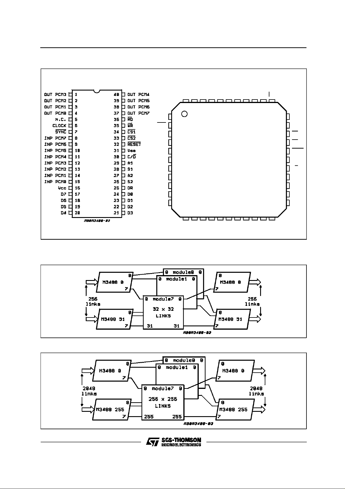
M348 8
PIN CO NNE CTI O NS (Top views)
N.C.
44 43 42 41 3940 38 37 36 35 34
OUT PCM0
OUT PCM1
OUT PCM2
OUT PCM3
N.C.
OUT PCM4
OUT PCM7
OUT PCM6
OUT PCM5
RD
1
2
3
4
5
D6
PQFP44
171118 19 20 21 22
D5
D4
D3
N.C.
D2
D1
D0
6
7
8
9
10
V
CC
12 13 14 15 16
D7
N.C.
DIP40
CLOCK
SYNC
INP PCM7
INP PCM6
INP PCM5
INP PCM4
INP PCM3
INP PCM2
INP PCM1
INP PCM0
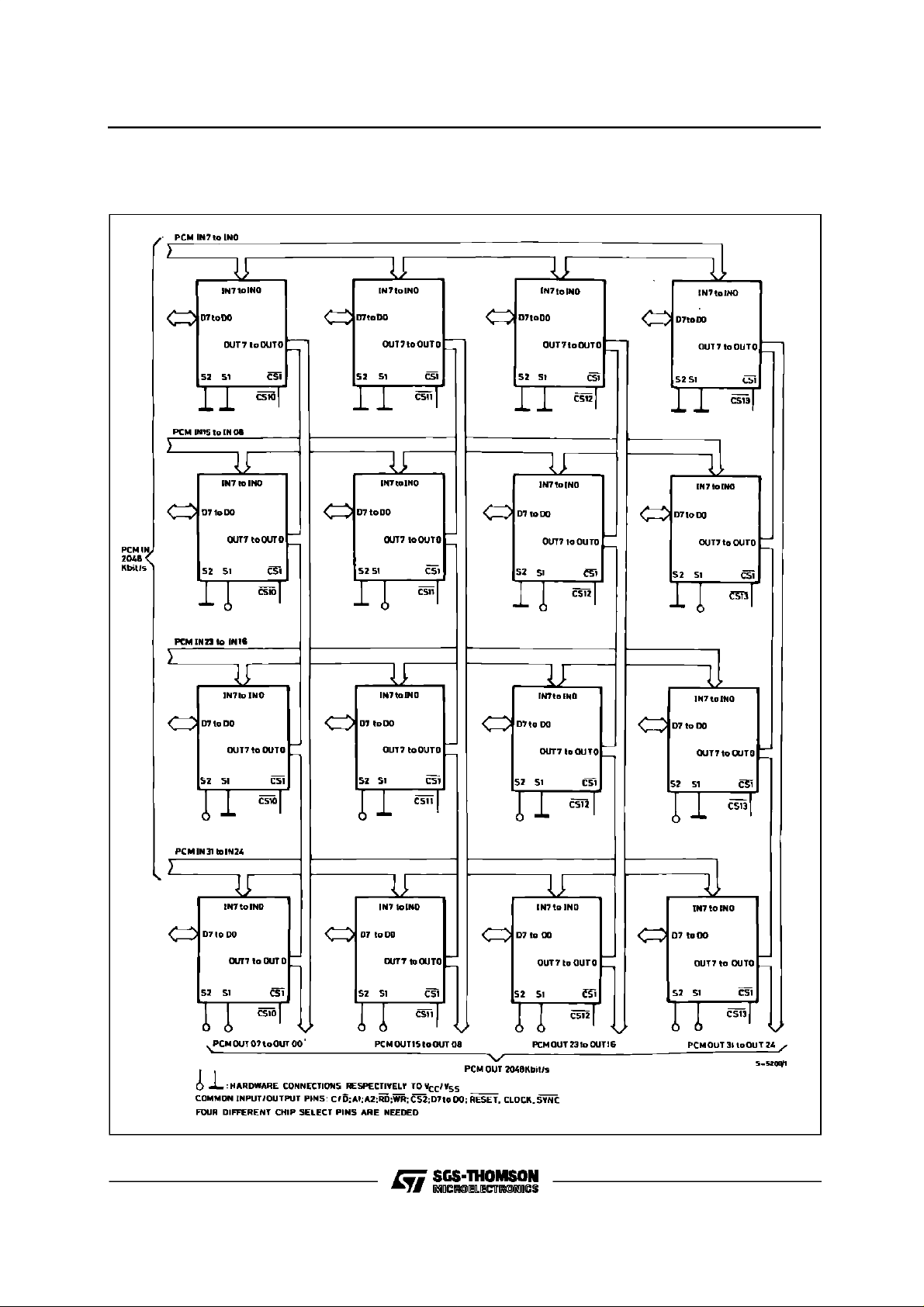
EXCHANGE NE TWORKS AP PLICATI O NS
256PCMlinks network (160or 192 DSM) : the 32 x 32 linkmoduleshown on the next page.
DR
33
32
31
30
29
28
27
26
25
24
23
D93TL040A
N.C.
WR
CS1
CS2
RESET
V
SS
C/D
A1
S1
A2
S2
2048PCM linksnetwork(1792or 2048 DSM) : the 256 x 256 link networkisshown above.
2/18
Page 3
EXCHANGE NET WORKS APPLICAT IO NS (continued)
SingleStage/SixteenDevices Configuration(32 by 32 links or 1024channels).
M3488
3/18
Page 4
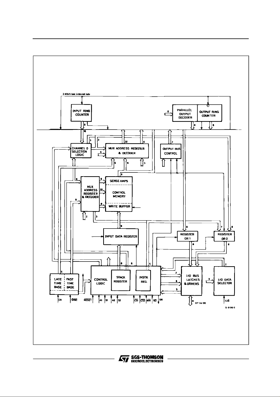
M348 8
BLOCK DIAGRAM
4/18
Page 5
M3488
RECOMMENDEDOPERATING CONDITIONS
Symbol Parameter Value Unit
V
CC
V
V
O
CLOCK
Freq.
SYNC Freq. Input Synchronization Frequency 8 KHz
T
op
CAPACITANCES (measurement freq. = 1MHz; Top= 0 to 70°C; unused pins tied to VSS)
Symbol Parameter Pins (*) Min. Typ. Max. Unit
C
C
I/O
C
Supply Voltage 4.75 to 5.25 V
Input Voltage 0 to 5.25 V
i
Off State Input Voltage 0 to 5.25 V
Input Clock Frequency
4.096 MHz
Operating Temperature 0 to 70 °C
Input Capacitance 6 to 15; 26 to 30; 32 to 36 5 pF
I
I/O Capacitance 20 to 24 15 pF
O
Output Capacitance 1 to 4; 17 to 19; 25; 37 to 40 10 pF
D.C. ELECTRICAL CHARACTERISTICS (T
All D.C. characteristics are valid 250µs after V
= 0 to 70°C, VCC=5V±5%)
amb
and clock have been applied.
CC
Symbol Parameter Pins (*) Test Condition Min. Typ. Max. Unit
V
ILC
V
IHC
V
IL
Clock Input Low Level 6 -0.3 0.8 V
Clock Input High Level 6 2.4 V
Input Low Level 7 to 15
-0.3 0.8 V
CC
20 to 24
26 to 30
32 to 36
V
IH
Input High Level 7 to 15
2V
CC
20 to 24
26 to 30
32 to 36
V
OH
I
OH
V
OL
I
OL
I
IL
Output High Voltage (Level)
17 to 25
Output High Current VOH= 2.4V 5 mA
Output Low Voltage (Level) 1 to 4
Output Low Current VOL= 0.4V 5 mA
37 to 40
17 to 25
Input Leakage Current 6 to 15
IOH= 5mA 2.4 V
IOL= 5mA 0.4 V
VIN= 0 to V
CC
5 µA
26 to 30
32 to 36
I
DL
Data Bus Leakage Current 17 to 24 VIN= 0 to V
CC
±5 µA
VCCapplied; Pins 35
and 36 tied to V
CC
,
after Device Initialization
I
CC
Supply Current 16 Clock Freq. = 4.096MHz 15 30 mA
V
V
(*) T he pin number is r ef erred to the D I P40 version.
5/18
Page 6
M348 8
A.C. ELECTRICAL CHARACTERISTICS (T
AllA.C. characteristi c sare valid250µs afterV
= 0 to 70°C, VCC=5V±5%)
amb
andclockhavebeenapplied.CListhe max. capacitiveload.
CC
Signal Symbol Parameter Test Condition Min. Typ. Max. Unit
CK (clock) t
SYNC
(framepulse)
PCM Input
Busses
PCM Output
Busses
Open Drain
CK
t
WL
t
WH
t
R
t
F
t
SL
t
HL
t
SH
t
WH
t
S
t
H
t
PD min
t
PD max
Clock Period
Clock Low Level Width
Clock High Level Width
Rise Time
Fall Time
Low Level Setup Time
Low Level Hold Time
High Level Setup Time
High Level Width
Setup Time
Hold Time
Propagation time
referred to CK low level
Propagation time
C
L
R
= 150pF
=1K
L
230
244
100
100
60
30
80
t
CK
5
+40
45 110
110 140
25
25
referred to CK high level
RESET t
WR, RD t
t
t
t
t
t
t
Low Level Setup Time
SL
t
Low Level Hold Time
HL
High Level Setup Time
SH
High level Width
WH
Low Lvel Width
WL
High Level Width
WH
Repetition Interval
REP
between Active Pulses
High Level Setup Time
SH
to Active Read Strobe
High Level Hold Time
HH
40 + 2 tCK+t
t
REP
+t
WL(CK)
R(CK)
+
60
30
80
t
CK
100
t
CK
see
formula
0
15
from Active Write Strobe
t
R
t
F
Rise Time
Fall Time
60
60
ns
ns
ns
ns
ns
ns
ns
ns
ns
ns
ns
ns
ns
ns
ns
ns
ns
ns
ns
ns
ns
ns
ns
ns
6/18
Page 7

A.C. ELECTRICAL CHARACTERISTICS (continued)
Signal Symbol Parameter Test Condition Min. Typ. Max. Unit
CS1, CS2 t
C/D t
A1, S1,
A2, S2
(match
inputs)
DR
(data
ready)
D0 to D7
(interface
bus)
SL(CS-WR)
t
HL(CS-WR)
t
SH(CS-WR)
t
HH(CS-WR)
t
SL(CS-RD)
t
HL(CS-RD)
t
SH(CS-RD)
t
HH(CS-RD)
S(C/D-WR)
t
H(C/D-WR)
t
S(C/D)-RD)
t
H(C/D-RD)
t
S(match-WR)
t
H(match-WR)
t
S(match-RD)
t
H(match-RD)
t
W
t
PD
t
S(BUS-WR)
t
H(BUS-WR)
Low level setup time
to WR falling edge
Low Level hold time
from WR rising edge
High Level setup time
to WR falling edge
High level hold time
from WR rising edge
Low level setup time
to RD falling edge
Low level hold time
from RD rising edge
High level setup time
RD falling edge
High level hold time
from RD
Setup time to write
strobe end
Hold time from
write strobe end
Setup time to read
strobe start
Hold time from read
strobe end
Setup time to write
strobe end
Hold time from
strobe end
Setup time to read
strobe start
Hold time from read
strobe end
Low state width
DR output delay
from write strobe end
(active command)
Input setup time to
write strobe end
Input hold time
from write strobe end
Active Case
Active Case
Inactive Case
Inactive Case
Active Case
Active Case
Inactive Case
Inactive Case
Instructions 5 and 6
Instruction5,C
=
L
150pF
130
130
4.t
130
15
20
20
15
20
20
15
0
0
0
0
0
0
0
0
2.t
CK
CK
7.t
CK
M3488
ns
ns
ns
ns
ns
ns
ns
ns
ns
ns
ns
ns
ns
ns
ns
ns
ns
ns
ns
ns
t
PD(BUS)
Propagation time
from (active) falling
C
L
= 200pF
120
Edge of read strobe
t
HZ(BUS)
Propagation time
from (active) rising
Edge of read strobe
CL= 200pF
80
to high impedance state
A.C. TESTING, OUTPUT WAVEFORM
A.C. testing inputs are driven at 2.4V for a logic ”1” and 0.45V for a logic ”0”, timing measurement are made at
2.0V for a logic ”1”and 0.8V for a logic ”0”.
ns
ns
7/18
Page 8

M348 8
PCM TIMING, RESET, SYNC
WRITE OPERATION TIMING
8/18
Page 9

READ OPERATION TIMING
M3488
GENERAL DES CRIPTIO N
TheM3488isintendedforlargetelephoneswitching
systems,mainlycentralexchanges,digitallineconcentratorsand private branch exchangeswhere a
distributed microcomputer control approach is extensively used. It consists of a speech memory
(SM),a controlmemory (CM), a serial/paralleland
a parallel/serial converter, an internal parallel bus,
an interface (8 data lines, 11 control signals) and
dedicatedcontrollogic.
Bymeansofrepeatedclock divisiontwotimebases
are generated. These are preset from an external
synchronization signal to two specific count numbersso that sequentialscanningof the basesgive
synchronous addresses to the memories and I/O
channelcontrols.Different preset count numbers
are needed because of processing delays and
datapathdirection.Thetimebasefortheinputchannels is delayed and the timebase for outputchannelsisadvancedwith respectto the actualtime.
EachserialPCMinput channelisconvertedtoparallel data and stored in the speech memory at the
beginning of any new time slot (according to first
timebase) in the location determined by input pin
numberand time slotnumber.The controlmemory
CM maintainsthe correspondencesbetween input
and output channels.More exactly,for any output
pin/outputchannelcombinationthecontrolmemory
giveseitherthefulladdressofthespeechmemory
location involved in the PCM transfer or an 8-bit
wordtobesuppliedto theparallel/serialoutputconverter.A9
th
bitateachCMlocationdefinesthedata
sourceforoutputlinks,lowfor SM,high forCM.
Thelatetimebaseis usedtoscantheoutputchan-
nelsandtodeterminethe pinsto beservicedwithin
eachchannel; enoughidle cyclesareleftto the microprocessorfor asynchronousinstructionprocessing.
Two8-bit registers OR1and OR2 supply feedback
datafor controlordiagnosticpurposes;OR1comes
frominternalbus i.e. frommemories,OR2gives an
opcode copyand additional data to the microcomputer. A four byte-five bit stack register and an instruction register, under microcomputer control,
storeinputdataavailableattheinterface.
Dedicatedlogic,undercontrolofthemicroprocessor
interface,extractsthe 0 channelcontentof anyselectedPCMinput bus, usingsparecycles of SM.
9/18
Page 10

M348 8
PINS FUNCTION
Symbol Name
D7 to D0 Data bus 17 to 24 13 to 21
C/D Input control 30 27
A1, S1, A2, S2 Address select or match 26 to 29 23 to 26
CS1, CS2 Chip select 33, 34 30, 31
WR Data transfer enable 35 32
RD Read enable 36 34
DR Data ready 25 22
RESET RESET control 32 29
Pin Assignement
DIP40 PQFP44
CLOCK Input master clock 6 1
SYNC Input synchronization 7 2
IN PCM 7 to 0 PCM input bus 8 to 15 3 to 10
OUT PCM 7
to 0
PCM output bus 37 to 40 and
1to4
35 to 38 and
40 to 43
10/18
Page 11

M3488
PIN DESCRIPTION
D7to D0
Databuspins.Thebidirectionalbusis usedtotransferdataandinstructionsto/fromthemicroprocessor.
D0 is theleastsignificantdigit. The output bus is 8
bits wide; inputis only 5 bits wide. (D4 to D0)
ThebusistristateandcannotbeusedwhileRESET
is heldlow.
Themeaningof inputdata, suchasbus or channel
numbers,and of expected output data is specified
indetailbytheinstructiondescription.(Pagg.12-14)
C/D(pin30)
Input control pin, select pin. In a write operation
C/D = 0 qualifies any bus content as data, while
C/D=1qualifiesitasanopcode.Inareadoperation
OR1isselected by C/D = 0, OR2 by C/D = 1.
A1,S1, A2, S2
Addressselect or matchpins. In a multi-chip configuration(e.g.asinglestagematrixexpansion),usingthesameCSpins,thematchcondition(A1=S1
andA2= S2)leavesthecommandinstructionasdefined;onthe contrarythe mismatchconditionmodifies the executionas follows : instructions1 and 3
arereversedto channeldisconnection,instruction5
is unaffected, instructions2-4-6 are cancelled (not
executed).
Busreadingtakes place only on match condition,
instructionflowis in any caseaffected.
Eachpinscoupleiscommutative:inamultichipconfigurationpins S1andS2giveahard-wiredaddress
selectionforindividualmatrixes,whileinsingle configuration S1 and A1 or S2 and A2 arenormally
tiedtogether.
CS1,CS2
Commutativechip select pins.Theyenablethe de-
vice to perform valid read/write operations(active
low). Two pins allow row/column selectionwith different types of microprocessors ; normally one is
tiedtoground.
RD
WhenCS1andCS2arelowandmatchconditionexists, a low level on RD enablesa registerOR1 or
OR2 readoperation,throughthebidirectionalbus.
In addition,the rising edge of RD latches C/D and
the matchconditionpinsinordertodirectthe internal flow of operations. Because of internal clock
resynchronization, one single additional requirement is recommendedin order to produce a simultaneousinstructionflowina multichipconfiguration:
theRD rising edgehasto be20to20+ t
WL(CK)
nsec
laterelative to clockfalling edge.
DR
Dataready.Normally high,DRoutputpin goeslow
to tell the microprocessorthat :
a) theinstructioncodewasfoundtobe invalid;
b) executing instruction5 an active outputchannel
was found in the whole matrix array, that is a CM
word not all ”ones” was found in a configurationof
devicessharingthesameCS pins;
c)executinginstruction6”0channelextraction”took
place and OR2 was loaded with total number of
messagesinserted on 0 timeslot.
DR is active lowabout two clock cycles in case b
andc ; in casea it is leftlowuntilavalidinstruction
code is supplied.
RESET
RESETcontrol pin is normallyused at the verybeginning to initialize the device or the network. Any
logicalstatusisresetandCM issettoall”ones”after
RESETgoing low.
The internal initialization routine takes one time
framewhatevertheRESETwidthonlowlevel(minimumonecycleroughly),butitisrepeatedaninteger
numberof time frames as long as RESETis found
lowduring0 timeslot.
Initializationpullstheinterfacebus immediatelyto a
highimpedancestate.After theCMhas beensetto
all ”ones”the PCM output channelsarealsoset to
high impedancestate.
WR
PinWR, when CS1andCS2arelow, enablesdata
transferfrom microprocessorto thedevice. Dataor
opcodeandcontrolsarelatchedon WRrisingedge.
Becauseofinternalclockresynchronizationonesingleadditionalrequirementisrecommendedin order
to produce a simultaneousinstruction executionin
amultichip configuration: WR rising edgehasto be
20to 20 + t
nseclate relative to clock falling
WL(CK)
edge.
CLOCK
Inputmaster clock.Typicalfrequencyis4.096MHz.
First division givesan internalclock controlling the
input andoutputchannelsbit rate.
SYNC
Input synchronization signal is active low. Typical
frequencyis 8kHz.
11/18
Page 12

M348 8
Internaltimebasesareforcedby synchronismtoan
assignedcount numberinorderto restore channels
and bit sequential addressing to a known state.
Count difference between the bases is 32, correspondingtotwotimeslots,thatistheminimumPCM
propagationtime, or latencytime.
INP PCM 7 to INP PCM 0
PCMinput bussesor pins;theyaccepta standard
2Mbit/srate. Bit 1 (sign bit) is the first of the serial
sequence; ina parallel conversionit isleft adjusted
as the mostsignificantdigit.
OUTPCM 7 to OUT PCM 0
PCMoutputbusses or pins ; bit rate and organizationarethesameas inputpins.
Outputbuffers are open drainCMOS.
Thedevicedrivesthe outputchannelstheoretically
one bit timebeforetheycanbeexploited as logical
input channels (bit and slot compatibility is preserved):this featureallowsinputsand outputsto be
tied together cancelling any analogdelay of digital
outputsup to
t
DEL max=tbit-tPD(PCM)max+tPD(PCM)min
MIXEDRDand WR OPERATIONS
In principle RD and WR operationsare allowedin
anyorderwithin specificationconstraints.
In practive,onlyone controlpinis low at any given
time whenCS1andCS2areenabled.
If by mistake or hardwarefailure both RD and WR
pins are low, the interfacebus is internallypushed
to tristatecondition as long as WR is heldlow and
input registersareprotected.
RegistersOR1and OR2 can be read in any order
with a single RD strobe using C/D as multiplexing
control; nevertheless thisprocedureisnot recommendedbecausethe device is directedforinstructionflowonlyaccordingto datalatchedbyRD rising
edge.
MultipleRDoperationsofthesamekindareallowed
without affecting the instruction flow : only ”new”
OR1 or OR2read operationsstep theflow.
Input and output registers are held for sure in the
previousstate for the first3 cyclesfollowing an opcode or an OR2 read.
FUNCTIONAL DES CRI PT I ON OF SPECIFIC MICROPROCESSOR OPERATIONS
Thedevice,undermicroprocessorcontrol,performs
the followinginstructions:
1CHANNEL CONNECTION
2CHANNEL DISCONNECTION
3LOADINGOFA BYTEONA PCMOUTPUT
CHANNEL
4 TRANSFEROFA SINGLEPCM OUTPUT
CHANNEL SAMPLE
5 TRANSFEROFA SINGLEOUTPUT
CHANNEL CONTROL WORD
6TRANSFEROFA SELECTED0CHANNEL PCM
INPUTDATA ACCORDINGTOAN 8-BITMASK
PREVIOUSLYSTOREDIN THE ”EXPECTED
MESSAGES”REGISTER
Afterthecodeis loadedin the instructionregisterit
is immediately checked to see whether it is acceptableand if not it is rejected.Ifaccepted the
instructionis alsoprocessedasregardsmatchcondition and is appended for execution during the
memories’sparecycles.
Fourcasesarepossible:
a)thecodeisnotvalid;executioncannottakeplace,
the DR outputpin is reset to indicate the error ; all
registersare saved ;
b) thecodeis validfor types 2,4 and6 butitis unmatched;executioncannottakeplace,DRisnotaffected.
c) the code is valid for types 1 and 3 and it is unmatched; theinstructionis interpretedas achannel
disconnection.
Theinstructionflowis asfollows.
Anyinputprotocolis startedby the microprocessor
interfaceloading the internal stack register with 2
bytes(4 bytes for instructions 1 and 3) qualifiedas
databytesbyC/D = 0 and a specificopcodequalified by C/D = 1 (match condition is normally
d) the code is validandis either matchedor of type
5 ; the instruction is processedas received.
Validationcontroltakesonly twocyclesoutof a total
executiontimeof4to7cycles;thelastoperationis
updatingof the contentof registersOR1and OR2,
accordingto the following instructiontables.
needed).
12/18
Page 13

M3488
During a verylong internaloperation(deviceinitialization after RESET going high or execution of instruction6)a new set of data byteswithavalidopcodeisacceptedwhilea wrongcodeis rejected.At
theendofthe currentroutineexecutiontakesplace
inthe samewayas describedbefore.
At the end of an instruction it is normally recommendedto readoneorboth registers. Toexploitinstruction6, however,itismandatoryto readregister
OR2.This is because instruction6, used between
othershortinstructionsoftype1to5, musthavepriorityandcanbe enabledonlyaftertheshortinstructionshave been completed.Instruction6 normally
hasa long processand a specialflowwhichis describedbelow.
First a not-all-zeromaskisstored in the ”expected
messages” register and in another ”background”
register. This operationstartsthe secondphase of
instruction6 which is called ”channel 0 extraction”
and is repeated at the beginning of any new time
frame.At thebeginningofthetimeframeanewcopy
ofactivatedchannelsto be extracted is madefrom
the ”backgroundregister”andput in the”expected
messages”register. Inadditionthelatterregister is
modifiedto indicatetheexactnumberof messages
that have arrived.The term messages coversany
input0channeldatawithstartingsequencedifferent
fromthe label01. So usingthis labelthenumberof
expectedmessagescan be reducedtocorrespond
to the number of effectivemessages.If and only if
theresidualnumberisdifferentfromzerowillthede-
vice start the extraction protocolat the end of the
currentroutine.
Theprocedureisasfollows:theDRoutputispulsed
low as a two cycle interrupt request and OR2 is
loadedwith the total number of active channels to
be extracted.
The transferof OR2 contentto the microprocessor
continuesthe extractionwhichconsistsofrepeated
steps of OR1 and OR2 loading, indicatingrespec-
tively the message and the incomingbus number.
Readingtheregistersin theorder OR1, OR2 must
becontinueduntilcompletionoruntilthe time frame
runs out.
Withanewtime frameanew extractionprocessbe-
gins, resuming the copy operation from the back-
groundregister.
Duringextraction the activechannelsare scanned
fromthehighesttothelowest number(from 7to 0).
Whileextractionisbeingcarriedoutthetimeinterval
requirementsbetweenactiverisingedgesofRDare
minimum 4 to 7 t
minimum2timest
for sequenceOR2 - OR1 and
CK
forsequenceOR1-OR2.More
CK
detailsare givenin the followingtables.
INSTRU CTIO N TABLES
Themostsignificantdigitsof OR2A7,A6,A5area
copyofthePCM selectedoutputbus; the leastsig-
nificantdigitsofOR2aretheopcode,C8 is thecon-
trolbit. Inanycaseparentheses()defineactualreg-
istercontent.
INSTRUCTION 1: CHANNELCONNECTION
Control Signals Data Bus
Match C/D CS WR RD D7 D6 D5 D4 D3 D2 D1 D0
X 0001XXXXXBi2Bi1Bi01
X 0 0 0 1 X X X Ci4 Ci3 Ci2 Ci1 Ci0 2
x 0001XXXXXBo2Bo1Bo03
X 0 0 0 1 X X X Co4 Co3 Co2 Co1 Co0 4th Data Byte: selected output channel.
yes/no 1 0 0 1 XXXX0001Instruction Opcode
C6
C5
C4
C3
C2
yes 0 0 1 0C7(1
(Bi2
yes 1 0 1 0A7(Bo2
(Bo2
1
Bi1
A6
Bo1
Bo1
1
Bi0
A5
Bo0
Bo0
1
Ci4
C8
1
0
1
Ci3
0
0
0
1
Ci2
0
0
0
C1
1
Ci1
0
0
0
st
Data Byte: selected input bus.
nd
Data Byte: selected input channel.
rd
Data Byte: selected output bus.
OR1: CM content copy, that is,
C0
1)
for mismatch condition,
Ci0)
for match condition
OR2: that is,
1
1)
for mismatch condition
1)
for match condition
Notes
13/18
Page 14

M348 8
INSTRUCTION2: OUTPUT CHANNEL DISCONNECTION
Control Signals Data Bus
Match C/D CS WR RD D7 D6 D5 D4 D3 D2 D1 D0
X 0 0 0 1 X X X X X Bo2 Bo1 Bo0 1
X 0 0 0 1 X X X Co4 Co3 Co2 Co1 Co0 2
st
Data Byte: selected output bus.
nd
Data Byte: selected output channel.
Notes
Yes 1 0 0 1 X X X X 0 0 1 0 Instruction Opcode
Yes001011111111
Yes1010
A7
(Bo2A6Bo1A5Bo01100111111)
OR1: CM Content Copy (output
channel is inactive)
OR2: that is.
INSTRUCTION3: LOADING ON A PCM OUTPUT CHANNEL FROM A MICROPROCESSOR BYTE
Control Signals Data Bus
Match C/D CS WR RD D7 D6 D5 D4 D3 D2 D1 D0
st
Data Byte: most significant digits to
X 0 0 0 1 X X X X X Ci7 Ci6 Ci5
X 0 0 0 1 X X X Ci4 Ci3 Ci2 Ci1 Ci0
X 0 0 0 1 X X X X X Bo2 Bo1 Bo0 3
1
be inserted.
nd
Data Byte: least significant digits to
2
be inserted.
rd
Data Byte: selected output bus.
X 0 0 0 1 X X X Co4 Co3 Co2 Co1 Co0 4th Data Byte: selected output channel..
Yes/no 1 0 0 1 X X X X 0 1 0 0 Instruction Opcode
OR1: CM content copy, that is,
C0
1)
for mismatch condition,
Ci0)
for match condition
OR2: that is.
Yes 0 0 1 0C7(1
(Ci7
Yes 1 0 1 0
A7
(Bo2A6Bo1A5Bo01100111111)
C6
1
Ci6
C5
1
Ci5
C4
1
Ci4
C3
1
Ci3
C2
1
Ci2
C1
1
Ci1
Notes
INSTRUCTION4: TRANSFER OF A SINGLE PCM SAMPLE
Control Signals Data Bus
Match C/D CS WR RD D7 D6 D5 D4 D3 D2 D1 D0
st
X 0 0 0 1 X X X X X Bo2 Bo1 Bo0 1
X 0 0 0 1 X X X Co4 Co3 Co2 Co1 Co0 2
Data Byte: selected output bus.
nd
Data Byte: selected output channel.
Yes 1 0 0 1 X X X X 1 0 1 1 Instruction Opcode
Yes0010
Yes1010
Notes : S7...S0 is a parallel copy of a PCM data, S7 is the most significant digit and the first of the sequence.
C7S7C6S6C5S5C4S4C3S3C2S2C1S1C0
A7
(Bo2A6Bo1A5Bo01100111111)
OR1: CM Content Copy if C8 = 1; or
S0
SM Content Sample if C8 = 0
OR2: that is.
Notes
14/18
Page 15

INSTRUCTION5: TRANSFER OF AN OUTPUT CHANNEL CONTROL WORD
M3488
Control Signals Data Bus
Match C/D CS WR RD D7 D6 D5 D4 D3 D2 D1 D0
X 0 0 0 1 X X X X X Bo2 Bo1 Bo0 1
X 0 0 0 1 X X X Co4 Co3 Co2 Co1 Co0 2
Yes 1 0 0 1 X X X X 1 0 0 0 Instruction Opcode
Yes 0 0 1 0 C7 C6 C5 C4 C3 C2 C1 C0 OR1: CM selected CM word copy.
Yes1010
A7
(Bo2A6Bo1A5Bo0C8C811000000)
st
Data Byte: selected output bus.
nd
Data Byte: selected output channel.
OR2: that is.
Notes
INSTRUCTION6: CHANNEL 0 SELECTION MASK STORE/DATA TRANSFER
Control Signals Data Bus
Match C/D CS WR RD D7 D6 D5 D4 D3 D2 D1 D0
X 0 0 0 1 X X X X X Mi7 Mi6 Mi5
X 0 0 0 1 X X X Mi4 Mi3 Mi2 Mi1 Mi0
Yes 1 0 0 1 X X X X 1 1 1 0 Instruction Opcode
Mask store control
Yes 0 0 1 0 (previous content) OR1: register is not affected.
Yes 1 0 1 0 N2 N1 N0 Tn 1 1 1 0 OR2: see below.
First Data Transfer (after DR going low)
Yes 0 0 1 0 (previous content) OR1: register is not affected.
Yes 1 0 1 0 N2 N1 N0 Tn 1 1 1 0 OR2: see below.
Repeated Data Transfer (after first OR2 transfer)
Yes 0 0 1 0 S7 S6 S5 S4 S3 S2 S1 S0 OR1: expected message stored in SM.
Yes 1 0 1 0 P2 P1 P0 Fn 1 1 1 0 OR2: see below.
st
Data Byte: most sign. digits of
1
selection mask.
nd
Data Byte: least sign. digits of
2
selection mask.
Notes
Notes : 1. About mask bitsMi0 to Mi7alogic ”0” level meansdisabling condition, a logic”1” level meansenabling condition.
M3488WITH LESS PCM LINKSTHAN32
CHANNELS
It is also possible to use M3488 when the PCM
framesaremadeup of a numberofchannelsother
than 32.
Supposethat the PCM frames are made up of NChannels,which will be numberedfrom0 to (N-1).
EachPCMframewill thusbe madeupof a number
of bits multiplied by 8 ; thisexactlyequal to (N
Also,inthiscase,it isnecessarytorespectthetimingrelationshipbetweenthe differentsignalsshown
on thedatasheet ; inparticular, arelation-shipisal-
2. A null maskor a RESET pulse clear the mask and thedeep background mask registers anddisable channel0 extraction function.
3. Reading of OR2is optionalaftermask storeor redefinition, because function isactivated only by not-null maskwriting.
4. After mask store (N2N1 N0)is thesumofactivatedchannels, afterDRis thesumofactivechannels ;Tn= 1/0means activation/suppressionof thefunction afterstore while afterDR onlyTn = 1canappearto tell a not-null configuration to beextracted.
5. Reading ofOR2 isimperativeafter DRin orderto stepthe datatransfer; reading ofOR1 is also neededto scanin descending order
the priorityregister. Relevantmessages only areconsidered, that meansonly messageswith a MSD label differentfrom 01.
6. (P2 P1P0) is thePCM bus onwhich themessage copied inOR1 wasfound; Fn is acontinuation bittelling respectively on level1/0
for anymore/no more extractionstep to beperformed.
SYNC and the first clock (CK) bit containedin the
slottime for bit 0 ofchannel0.
Inorder to use M3488 with these frames,itis sufficient,usingthedatabytessentby themicroprocessor, tomodifythe numberingof a few channels.
In particular:
a)in allinstructionsinwhichreferenceismadetothe
.
8).
input channel (N-1), the number 31 should be
substitutedforthenumber (N-1) ;
b)in allinstructionsinwhichreferenceismadetothe
output channel0, the number N should be substitutedfor the number0.
ways carefully made between the rising edge of
15/18
Page 16

M348 8
PQFP44 (10 x 10) PACKAGE MECHANICAL DATA
DIM.
mm inch
MIN. TYP. MAX. MIN. TYP. MAX.
A 2.45 0.096
A1 0.25 0.010
A2 1.95 2.00 2.10 0.077 0.079 0.083
B 0.30 0.45 0.012 0.018
c 0.13 0.23 0.005 0.009
D 12.95 13.20 13.45 0.51 0.52 0.53
D1 9.90 10.00 10.10 0.390 0.394 0.398
D3 8.00 0.315
e 0.80 0.031
E 12.95 13.20 13.45 0.510 0.520 0.530
E1 9.90 10.00 10.10 0.390 0.394 0.398
E3 8.00 0.315
L 0.65 0.80 0.95 0.026 0.031 0.037
L1 1.60 0.063
K0°(min.), 7°(max.)
D
D1
2333
11
PQFP44
22
L1
E
L
E3D3E1
12
0.10mm
.004
Seating Plane
K
34
B
44
1
e
A1
B
A
A2
C
16/18
Page 17

DIP40 PACKAGE MECHANICAL DATA
M3488
DIM.
MIN TYP MAX MIN TYP MAX
a1 0.63 0.025
b 0.45 0.018
b1 0.23 0.31 0.009 0.012
b2 1.27 0.050
D 52.58 2.070
E 15.2 16.68 0.598 0.657
e 2.54 0.100
e3 48.26 1.900
F 14.1 0.555
I 4.445 0.175
L 3.3 0.130
mm inch
17/18
Page 18

M348 8
Information furnished is believed to be accurate and reliable. However, SGS-THOMSON Microelectronics assumes no responsibility for
the consequences of use of such information nor for any infringement of patents or other rights of third parties which may result from its
use. No license is granted by implication or otherwise under any patent or patent rights of SGS-THOMSON Microelectronics. Specification
mentioned in this publication are subject to change without notice. This publication supersedes and replaces all information previously
supplied. SGS-THOMSON Microelectronics products are not authorized for use as critical components in life support devices or systems
without express written approval of SGS-THOMSON Microelectronics.
1996 SGS-THOMSON Microelectronics – Printed in Italy – All Rights Reserved
SGS-THOMSON Microelectronics GROUP OF COMPANIES
Australia - Brazil - Canada - China - France - Germany - Hong Kong - Italy - Japan - Korea - Malaysia - Malta - Morocco -
The Netherlands - Singapore - Spain - Sweden - Switzerland - Taiwan - Thailand - United Kingdom - U.S.A.
18/18
 Loading...