

Datasheet M34570M4-XXXFP, M34570EDFP, M34570E8FP, M34570MD-XXXFP, M34570M8-XXXFP Datasheet (Mitsubishi)
Page 1
DESCRIPTION
The 4570 Group is a 4-bit single-chip microcomputer designed
with CMOS technology. Its CPU is that of the 4500 series using
a simple, high-speed instruction set. The computer is equipped
with a carrier wave output circuit for remote control, an 8-bit timer
with a reload register, a 10-bit timer with a reload register, and
an 8-bit timer with two reload registers.
The various microcomputers in the 4570 Group include variations
of the built-in memory size. The mask ROM version and One
Time PROM version of 4570 Group are produced as shown in
the table below.
FEATURES
●Minimum instruction execution time
When f(X
(f(X
When f(X
(f(X
●Supply voltage
............................. 2.5 V to 5.5 V (One Time PROM version)
.......................................2.0 V to 5.5 V (Mask ROM version)
IN) is selected for system clock.......................1.5
IN)=2.0 MHz, VDD=4.5 V to 5.5 V)
IN)/4 is selected for system clock................. 2.86
IN)=4.2 MHz, VDD=2.0 V to 5.5 V)
µ
µ
MITSUBISHI MICROCOMPUTERS
4570 Group
SINGLE-CHIP 4-BIT CMOS MICROCOMPUTER
●System clock switch function
.............................................................f(X
●Timers
Timer 1... 10-bit timer with a reload register and carrier wave
output auto-control function
Timer 2 ................................8-bit timer with a reload register
Timer 3... 8-bit timer with two reload registers and carrier wave
generation function
●Interrupt ...................................................................4 sources
●Power-on reset circuit
●Watchdog timer ............................................................16 bits
●Key-on wakeup function (Ports P0, P1, and P4, ON/OFF of
port P4 can be switched)
●Pull-up transistor.............. (Ports P0, P1, and P4, ON/OFF of
s
port P4 can be switched)
●Voltage drop detection circuit
s
●Clock generating circuit (ceramic resonance)
APPLICATION
Remote control transmitter
IN)/4 or not divided
Product
M34570M4-XXXFP
M34570M8-XXXFP
M34570MD-XXXFP
M34570E8FP
M34570EDFP *
*: Under development (Jan. 1999)
ROM (PROM) size
(✕ 10 bits)
4096 words
8192 words
16384 words
8192 words
16384 words
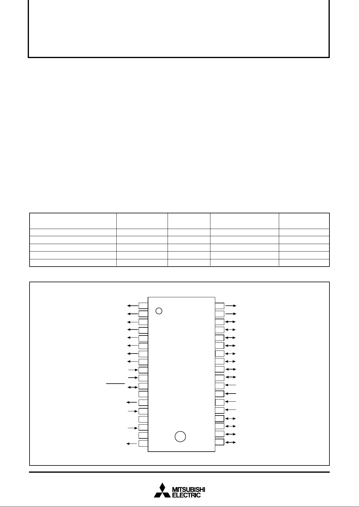
PIN CONFIGURATION (TOP VIEW)
M34570Mx-XXXFP
D9/T
P21/INT
RESET
CNV
X
VDCE
CARR
D
D
D
D
D
D
D
OUT
P2
SS
OUT
X
IN
V
SS
V
DD
2
3
4
5
6
7
8
0
10
11
12
13
14
15
16
17
18
RAM size
(✕ 4 bits)
128 words
128 words
128 words
128 words
128 words
1
2
3
4
M34570Mx-XXXFP
5
6
7
8
9
36
35
34
33
32
31
30
29
28
27
26
25
24
23
22
21
20
19
Package
36P2R-A
36P2R-A
36P2R-A
36P2R-A
36P2R-A
D
1
D
0
P1
3
P1
2
P1
1
P1
0
P0
3
P0
2
P0
1
P0
0
P4
3
P4
2
P4
1
P4
0
P3
3
P3
2
P3
1
P3
0
ROM type
Mask ROM
Mask ROM
Mask ROM
One Time PROM
One Time PROM
Outline 36P2R-A
Page 2
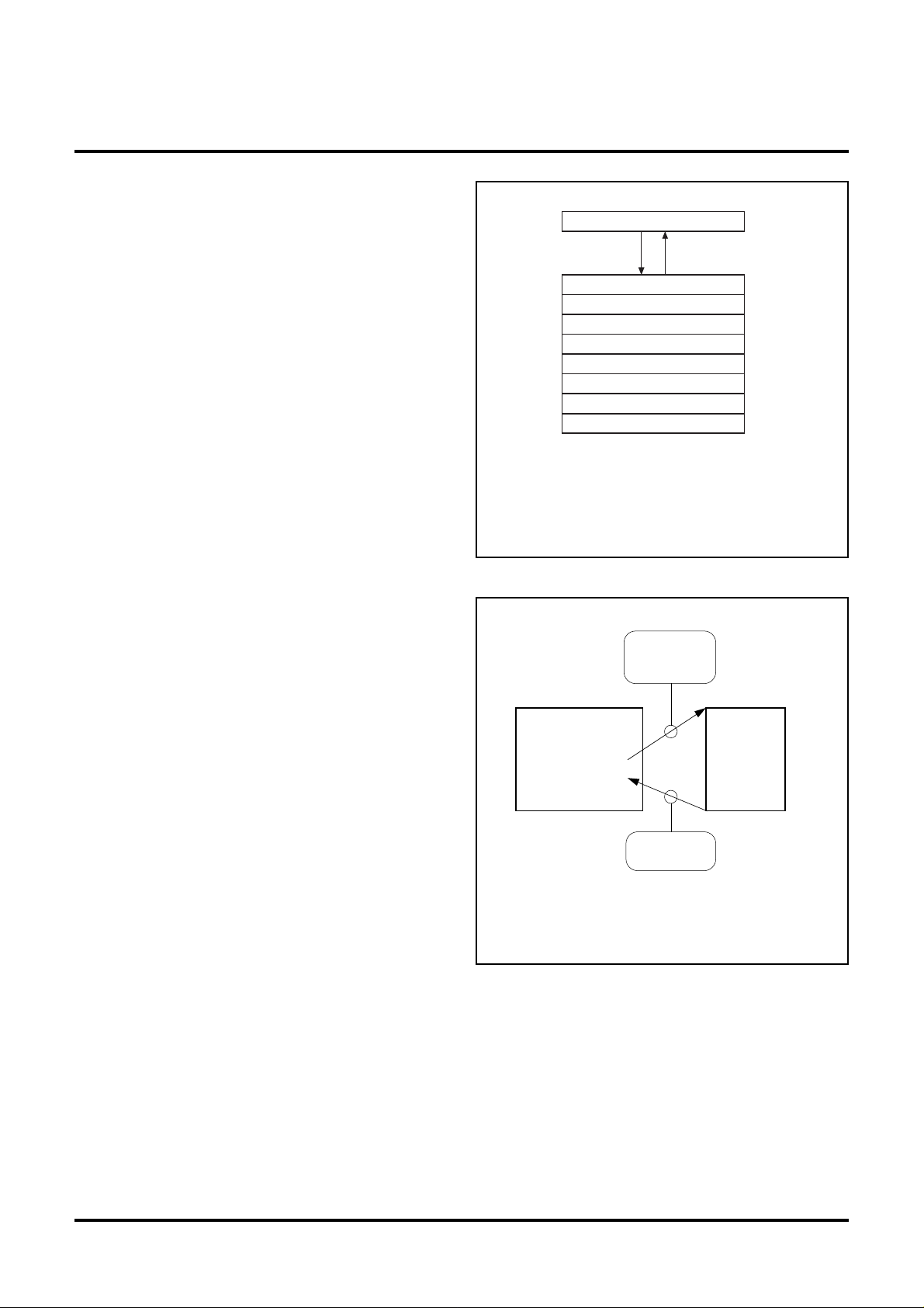
BLOCK DIAGRAM
10
Port D
MITSUBISHI MICROCOMPUTERS
4570 Group
SINGLE-CHIP 4-BIT CMOS MICROCOMPUTER
OUT
–X
IN
X
4
Port P4
4
Port P3
2
Port P2
Clock generating circuit
Reset (Voltage drop detection circuit)
Memory
ROM (Note)
4096 to 16384 words ✕ 10 bits
CPU core
ALU(4 bits)
RAM
128 words ✕ 4 bits
Register B (4 bits)
Register E (8 bits)
4500 Series
Stack registers SKs (8 levels)
Interrupt stack register SDP(1 level)
Register D (3 bits)
Register A (4 bits)
4
Note: PROM 16384 words ✕ 10 bits for the built-in PROM version.
Port P1
4
Port P0
Timers/Carrier wave generation
Timer 2 (8 bits)
Timer 3 (8 bits)
Timer 1 (10 bits)
(Carrier wave generation)
Watchdog timer (16 bits)
Internal peripheral functions
I/O port
2
Page 3
PERFORMANCE OVERVIEW
Parameter
Number of basic instructions
Minimum instruction execution time
Memory sizes
ROM
RAM
Input/Output
ports
0–D9
D
P00–P03
P10–P13
P20, P21
P30–P33
P40–P43
CARR
OUT
T
INT
Timers
Timer 1
Timer 2
Timer 3
Interrupt
Sources
Nesting
Subroutine nesting
Device structure
Package
Operating temperature range
Supply voltage
Power
at active
dissipation
(typical value)
at RAM back-up
M34570M4
M34570M8
M34570MD
M34570E8
M34570ED
Output
I/O
I/O
Input
I/O
Input
Output
Output
Input
MITSUBISHI MICROCOMPUTERS
4570 Group
SINGLE-CHIP 4-BIT CMOS MICROCOMPUTER
Function
99
µ
s (f(XIN) = 2.0 MHz:system clock = f(XIN): VDD = 5.0 V)
1.5
µ
s (f(XIN) = 4.2 MHz:system clock = f(XIN)/4: VDD = 5.0 V)
2.86
4096 words ✕ 10 bits
8192 words ✕ 10 bits
16384 words ✕ 10 bits
8192 words ✕ 10 bits
16384 words ✕ 10 bits
128 words ✕ 4 bits
Ten independent output ports; port D
4-bit I/O port; every pin of the ports has a key-on wakeup function and a pull-up function.
4-bit I/O port; every pin of the ports has a key-on wakeup function and a pull-up function.
2-bit input port, port P2
1 is also used as INT input pin.
4-bit I/O port
4-bit input port; both pull-up function and key-on wakeup function can be switched by software.
1-bit output port (CMOS output)
1-bit output pin; T
OUT output pin is also used as port D9.
1-bit input pin with a key-on wakeup function. INT input pin is also used as port P2
10-bit timer with a reload register and carrier wave output auto-control function
8-bit timer with a reload register
8-bit timer with two reload registers and carrier wave generation function
4 (one for external and three for timer)
1 level
8 levels (however, only 7 levels can be used when an interrupt is used or the TABP p instruction
is executed)
CMOS silicon gate
36-pin plastic molded SSOP
–20 °C to 70 °C
2.0 V to 5.5 V for mask ROM version (2.5 V to 5.5 V for One Time PROM version)
1.3 mA (f(X
0.5 mA (f(X
µ
0.1
IN) = 4.2 MHz: system clock = f(XIN)/4, VDD=5.0 V)
IN) = 1.0 MHz: system clock = f(XIN), VDD=3.0 V)
A (Ta=25 °C, VDD=5V, typical value)
9 is also used as the TOUT output pin.
1.
DEFINITION OF CLOCK AND CYCLE
●System clock
The system clock is the basic clock for controlling this product.
The system clock can be selected by bit 3 of the clock control
register MR as shown in the table below.
Table Selection of system clock
MR3
Note: f(X
from reset.
f(X
f(X
IN)
IN)/4
0
1
IN)/4 is selected immediately after system is released
System clock
●Instruction clock
The instruction clock is the standard clock for controlling CPU.
The instruction clock is a signal derived from dividing the
system clock by 3. The one cycle of the instruction clock is
equivalent to the one machine cycle.
●Machine cycle
The machine cycle is the standard cycle required to execute
the instruction.
3
Page 4
PIN DESCRIPTION
Pin
DD
V
VSS
CNVSS
RESET
XIN
XOUT
D0–D9
P00–P03
P10–P13
P20, P21
P30–P33
P40–P43
CARR
INT
OUT
T
VDCE
Name
Power supply
Ground
SS
CNV
Reset input
Clock input
Clock output
Output port D
I/O port P0
I/O port P1
Input port P2
I/O port P3
Input port P4
Carrier wave output
for remote control
Interrupt input
Timer output
Voltage drop
detection circuit
enable
Input/Output
—
—
Input
I/O
Input
Output
Output
I/O
I/O
I/O
I/O
Input
Output
Input
Output
Input
MITSUBISHI MICROCOMPUTERS
4570 Group
SINGLE-CHIP 4-BIT CMOS MICROCOMPUTER
Function
Connected to a plus power supply.
Connected to a 0 V power supply.
Connect CNV
An N-channel open-drain I/O pin for a system reset. A pull-up transistor and a
capacitor are built-in this pin. When the watchdog timer causes the system to be
reset or the low-supply voltage is detected, the
I/O pins of the clock generating circuit. Connect a ceramic resonator between X
pin and XOUT pin. A feedback resistor is built-in between them.
Each pin of port D has an independent 1-bit wide output function. Port D
used as T
4-bit I/O port. It can be used as an input port when the output latch is set to “1.”
The output structure is N-channel open-drain. Every pin of the ports has a key-on
wakeup function and a pull-up function.
4-bit I/O port. It can be used as an input port when the output latch is set to “1.”
The output structure is N-channel open-drain. Every pin of the ports has a key-on
wakeup function and a pull-up function.
2-bit input port. Port P2
4-bit I/O port. It can be used as an input port when the output latch is set to “1.”
The output structure is N-channel open-drain.
4-bit input port. Every pin of the ports has a key-on wakeup function and a pull-up
function. Both functions can be switched by software.
Carrier wave output pin for remote control transmit. The output structure is the
CMOS circuit.
INT input pin accepts an external interrupt and has a key-on wakeup function. INT
input pin is also used as port P2
OUT output pin has the function to output the timer 2 underflow signal divided by
T
OUT output pin is also used as port D9.
2. T
VDCE pin is used to control the operation/stop of the voltage drop detection circuit.
The circuit is operating when “H” level is input to the VDCE pin. It is stopped when
“L” level is input to this pin.
SS to VSS and apply “L” (0V) to CNVSS certainly.
RESET pin outputs “L” level.
9 is also
OUT output pin. The output structure is N-channel open-drain.
1 is also used as the INT input pin.
1.
IN
4
Page 5
MITSUBISHI MICROCOMPUTERS
4570 Group
SINGLE-CHIP 4-BIT CMOS MICROCOMPUTER
MULTIFUNCTION
Pin
9
D
P21
OUT
T
INT
Notes 1: Pins except above have just single function.
2: The port D
9 is the output port and port P21 is the input port.
CONNECTIONS OF UNUSED PINS
Pin
0–D8
D
D9/TOUT
P00–P03
P10–P13
P20, P21/INT
Notes 1: When the P21/INT pin is connected to VSS pin, set the return level to “H” level by software (interrupt control register I12=“1”).
When the P2
state immediately after system enters the RAM back-up state.
2: In order to connect ports P4
also invalidate the key-on wakeup functions (key-on wakeup control register K0i=“0”). When these pins are connected to
V
SS while the key-on wakeup functions are left valid, the system fails to return from RAM back-up state. In order to make
these pins open, turn on their pull-up transistors (register PU0i=“1”) by software (i = 0, 1, 2, 3).
Be sure to select the key-on wakeup function and the pull-up function with every one port.
3: In order to make ports P4
Connect to V
“0” and open.
Set the output latch to “1” and open.
Connect to V
1/INT pin is connected to VSS pin while the return level is set to “L” level, system returns from RAM back-up
Multifunction
Connection
SS, or set the output latch to
T
INT
P3
OUT
0–P33
Pin
Pin
9
D
P21
Connect to V
Multifunction
Connection
SS, or set the output latch to
“0” and open.
P40–P43
CARR
SS (Note 1).
0–P43 to VSS, turn off their pull-up transistors (pull-up control register PU0i=“0”) by software and
0–P43 open, turn on their pull-up transistors (register PU0i = “1”) by software (i = 0, 1, 2, 3).
Connect to V
Open.
SS (Note 2) or open (Note 3).
(Note in order to set the output latch to “0” or “1” or make pins open)
• After system is released from reset, a port is in a high-impedance state until the output latch of the port is set to “0” by software.
Accordingly, the voltage level of pins is undefined and the excess of the supply current may occur.
• To set the output latch periodically is recommended because the value of output latch may change by noise or a program run away
(caused by noise).
(Note in order to connect unused pins to V
• To avoid noise, connect the unused pins to V
SS)
SS at the shortest distance using a thick wire.
PORT FUNCTION
Port
Port D
Pin
D
0–D8, D9/TOUT
Input/
Output
Output
Output structure
N-channel open-drain
Control
bits
(10)
Port P0
P00–P03
I/O
N-channel open-drain
(4)
Port P1
P10–P13
I/O
N-channel open-drain
(4)
Port P2
P20
Input
(2)
P21/INT
Port P3
Port P4
0–P33
P3
P40–P43
I/O
Input
N-channel open-drain
(4)
Note: Level of the P21/INT pin can be examined with the SNZI0 instruction.
1
4
4
2
4
4
Control
instructions
SD
RD
CLD
OP0A
IAP0
OP1A
IAP1
IAP2
SNZI0
(Note)
OP3A
IAP3
IAP4
Control
registers
2
W2
PU0
K0
Remark
W22 controls the switch of D9/
OUT pin
T
Pull-up functions
Key-on wakeup functions
Pull-up functions
Key-on wakeup functions
Key-on wakeup function
Pull-up functions
(programmable)
Key-on wakeup functions
(programmable)
5
Page 6
PORT BLOCK DIAGRAMS
MITSUBISHI MICROCOMPUTERS
4570 Group
SINGLE-CHIP 4-BIT CMOS MICROCOMPUTER
Key-on wakeup
Register A
(Note 2)
Key-on wakeup
Register A
(Note 2)
Key-on wakeup
input
Register A
input
Ai
OP0A instruction
input
Ai
OP1A instruction
K00
IAP4 instruction
IAP0 instruction
Q
D
T
IAP1 instruction
DTQ
Pull-up
transistor
PU00
Pull-up
transistor
Pull-up
transistor
(Note 1)
P40
(Note 1)
(Note 1)
P00–P03
P10–P13
Register A
(Note 2)
Register A
Key-on wakeup
Register A
instruction
input
IAP3 instruction
Ai
OP3A
IAP2 instruction
External interrupt circuit
IAP2 instruction
D
Q
T
P20
(Note 1)
P21/INT
(Note 1)
P30–P33
(Note 1)
Key-on wakeup
Key-on wakeup
Key-on wakeup
input
Register A
input
Register A
input
Register A
K01
IAP4 instruction
K02
IAP4 instruction
K03
IAP4 instruction
Pull-up
transistor
PU01
Pull-up
transistor
PU02
Pull-up
transistor
PU03
(Note 1)
(Note 1)
(Note 1)
Register Y
SD instruction
RD instruction
P41
Register Y
SD instruction
RD instruction
Timer 2 underflow signal output
P42
Notes 1.
P43
Decoder
CLD
instruction
Decoder
CLD
instruction
This symbol represents a parasitic diode.
Applied potential to ports P2
2. i represents 0, 1, 2 or 3.
S
RQ
S
W22
RQ
1/2
0
1
0 and P21 must be VDD or less.
D0–D8
(Note 1)
D9/TOUT
(Note 1)
6
Page 7
PORT BLOCK DIAGRAMS (continued)
MITSUBISHI MICROCOMPUTERS
4570 Group
SINGLE-CHIP 4-BIT CMOS MICROCOMPUTER
Timer 2 underflow
signal
ORCLK
X
Register B Register A
(T3HAB)
Reload register R3H (8)
W31,W3
0
W3
00
01
10
MR
3
IN
1/2
11
0
Not available
1
0
1
(TAB3)
3
(T3AB)
Reload register R3L (8)
Register B Register A
Timer 3(8)
(T3AB)
Timer 1 underflow
signal
Reload control circuit
(TAB3)
C2
0
Q
T
R
W3
3
Q
T
R
W1
0
To timer 1
C2
1
CARRY
(Note)
Port CARR
T3F
This symbol represents a parasitic diode.Note :
Timer 3
interrupt
7
Page 8
FUNCTION BLOCK OPERATIONS
CPU
(1) Arithmetic logic unit (ALU)
The arithmetic logic unit ALU performs 4-bit arithmetic such
as 4-bit data addition, comparison, AND operation, OR
operation, and bit manipulation.
(2) Register A and carry flag (CY)
Register A is a 4-bit register used for arithmetic, transfer,
exchange, and I/O operation.
Carry flag CY is a 1-bit flag that is set to “1” when there is a
carry with the AMC instruction (Figure 1).
It is unchanged with both A n instruction and AM instruction.
The value of A
instruction (Figure 2).
Carry flag CY can be set to “1” with the SC instruction and
cleared to “0” with the RC instruction.
(3) Registers B and E
Register B is a 4-bit register used for temporary storage of 4bit data, and for 8-bit data transfer together with register A.
Register E is an 8-bit register. It can be used for 8-bit data
transfer with register B used as the high-order 4 bits and
register A as the low-order 4 bits (Figure 3).
0 is stored in carry flag CY with the RAR
MITSUBISHI MICROCOMPUTERS
4570 Group
SINGLE-CHIP 4-BIT CMOS MICROCOMPUTER
<Carry>
(CY)
(M(DP))
Addition
(A)
Fig. 1 AMC instruction execution example
<Set>
SC instruction
<Clear>
RC instruction
CY A3A2A1A
A
0
Fig. 2 RAR instruction execution example
ALU
<Result>
<Rotation>
RAR instruction
CY A3A2A
0
1
(4) Register D
Register D is a 3-bit register.
It is used to store a 7-bit ROM address together with register
A and is used as a pointer within the specified page when the
TABP p, BLA p, or BMLA p instruction is executed (Figure 4).
TABP p instruction
Specifying address
PC
H
p6p5p4p3p2p1p
Immediate field
value p
DR2DR1DR
0
The contents of
register D
PC
L
0
A3A2A1A
The contents of
register A
Register B Register A
B3B2B1B
Register E
E7E6E5E4E3E2E1E
B3B2B1B
Register B Register A
TAB instruction
0
TEAB instruction
TABE instruction
0
TBA instruction
A3A2A1A
A3A2A1A
Fig. 3 Registers A, B and register E
ROM
840
Low-order 4 bits
0
Middle-order 4 bits
High-order 2 bits
Register W5 (2)
0
0
0
Register A (4)
Register B (4)
Register B (4)
Fig. 4 TABP p instruction execution example
8
Page 9
MITSUBISHI MICROCOMPUTERS
4570 Group
SINGLE-CHIP 4-BIT CMOS MICROCOMPUTER
(5) Stack registers (SK
S) and stack pointer (SP)
Stack registers (SKs) are used to temporarily store the
contents of program counter (PC) just before branching until
returning to the original routine when;
• branching to an interrupt service routine (referred to as
an interrupt service routine),
• performing a subroutine call, or
• executing the table reference instruction (TABP p).
Stack registers (SKs) are eight identical registers, so that
subroutines can be nested up to 8 levels. However, one of
stack registers is used when using an interrupt service routine
or when executing a table reference instruction. Accordingly,
be careful not to stack over when performing these operations
together. The contents of registers SKs are destroyed when
8 levels are exceeded.
The register SK nesting level is pointed automatically by 3bit stack pointer (SP). The contents of the stack pointer (SP)
can be transferred to register A with the TASP instruction.
Figure 5 shows the stack registers (SKs) structure.
Figure 6 shows the example of operation at subroutine call.
(6) Interrupt stack register (SDP)
Interrupt stack register (SDP) is a 1-stage register. When an
interrupt occurs, this register (SDP) is used to temporarily
store the contents of data pointer, carry flag, skip flag, register
A, and register B just before an interrupt until returning to the
original routine.
Unlike the stack registers (SKs), this register (SDP) is not
used when executing the subroutine call instruction and the
table reference instruction.
(7) Skip flag
Skip flag controls skip decision for the conditional skip
instructions and continuous described skip instructions. When
an interrupt occurs, the contents of skip flag is stored
automatically in the interrupt stack register (SDP) and the
skip condition is retained.
Program counter (PC)
Executing the subroutine
call or table reference
instruction
Executing the return or
table reference instruction
SK0
SK1
SK2
SK3
SK4
SK5
SK6
SK7
Stack pointer (SP) points “7” at reset or
returning from RAM back-up mode. It points “0”
by executing the first BM instruction, and the
contents of program counter is stored in SK
When the BM instruction is executed after eight
stack registers are used ((SP) = 7), (SP) = 0
and the contents of SK
0 is destroyed.
Fig. 5 Stack registers (SKs) structure
➝
(SP) 0
➝
(SK
0
) 0001
➝
(PC) SUB1
Main program
Address
16
NOP
0000
0001
16
BM SUB1
000216 NOP
16
Subroutine
SUB1 :
(SP) = 0
(SP) = 1
(SP) = 2
(SP) = 3
(SP) = 4
(SP) = 5
(SP) = 6
(SP) = 7
NOP
·
·
·
RT
0.
➝
(PC) (SK0)
➝
(SP) 7
Note:
Returning to the BM instruction execution
address with the RT instruction, and the BM
instruction is equivalent to the NOP instruction.
Fig. 6 Example of operation at subroutine call
9
Page 10
(8) Program counter (PC)
Program counter (PC) is used to specify a ROM address (page
and address). It determines a sequence in which instructions
stored in ROM are read. It is a binary counter that increments
the number of instruction bytes each time an instruction is
executed. However, the value changes to a specified address
when branch instructions, subroutine call instructions, return
instructions, or the table reference instruction (TABP p) is
executed.
Program counter consists of PC
7) which specifies to a ROM page and PC
H (most significant bit to bit
L (bits 6 to 0) which
specifies an address within a page. After it reaches the last
address (address 127) of a page, it specifies address 0 of the
next page (Figure 7).
Make sure that the PC
H does not specify after the last page
of the built-in ROM.
(9) Data pointer (DP)
Data pointer (DP) is used to specify a RAM address and
consists of registers Z, X, and Y. Register Z specifies a RAM
file group, register X specifies a file, and register Y specifies
a RAM digit (Figure 8).
Register Y is also used to specify the port D bit position.
When using port D, set the port D bit position to register Y
certainly and execute the SD or RD instruction (Figure 9).
MITSUBISHI MICROCOMPUTERS
SINGLE-CHIP 4-BIT CMOS MICROCOMPUTER
Program counter (PC)
p5p4p3p2p1p0a6a5a4a3a2a1a
p
6
PC
H
Specifying page
Fig. 7 Program counter (PC) structure
Data pointer (DP)
Z1Z0X3X2X1X0Y3Y2Y1Y
Register X (4)
Register Z (2)
Specifying address
Register Y (4)
Specifying RAM file
Specifying RAM file group
4570 Group
0
PC
L
0
Specifying
RAM digit
Fig. 8 Data pointer (DP) structure
Specifying bit position
D
9
D
6
0101 1
Register Y (4)
Port D output latch
Fig. 9 SD instruction execution example
Set
D
5
D
0
D
4
10
Page 11

MITSUBISHI MICROCOMPUTERS
4570 Group
SINGLE-CHIP 4-BIT CMOS MICROCOMPUTER
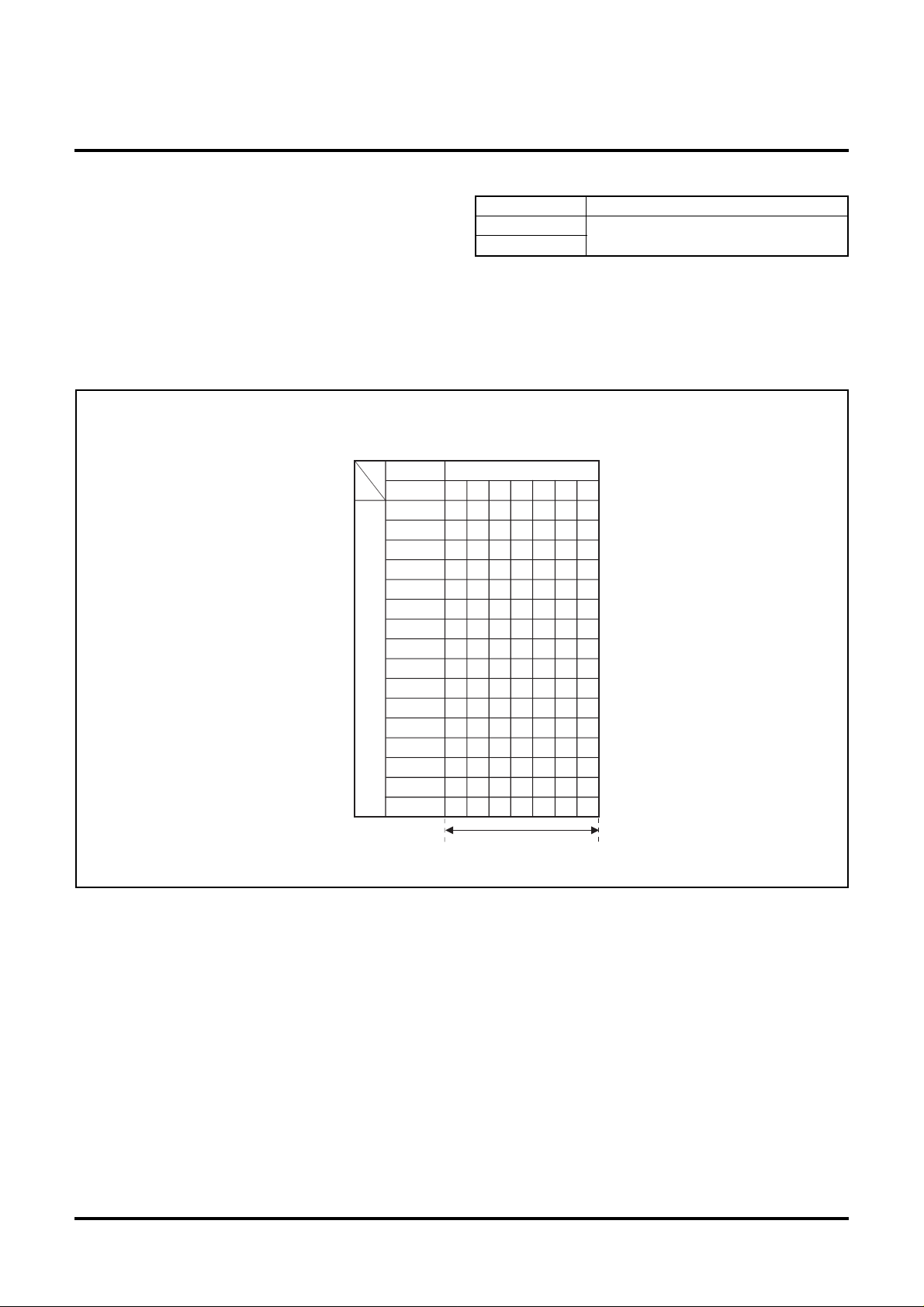
PROGRAM MEMORY (ROM)
1 word of ROM is composed of 10 bits. ROM is separated every
128 words by the unit of page (addresses 0 to 127). Table 1
shows the ROM size and pages. Figure 10 shows the ROM map
of M34570M8.
Table 1 ROM size and pages
Product
M34570M4
M34570M8
M34570E8
M34570MD
M34570ED
Note: When the TABP instruction is executed after executing
the SBK instruction, data in pages 64 to 127 can be
referred. When the TABP instruction is executed after
executing the RBK instruction, data in pages 0 to 63 can
be referred.
A top part of page 1 (addresses 0080
for interrupt addresses (Figure 11). When an interrupt occurs,
the address (interrupt address) corresponding to each interrupt
is set in the program counter, and the instruction at the interrupt
address is executed. When using an interrupt service routine,
write the instruction generating the branch to that routine at an
interrupt address.
Page 2 (addresses 0100
subroutine calls. Subroutines written in this page can be called
from any page with the 1-word instruction (BM). Subroutines
extending from page 2 to another page can also be called with
the BM instruction when it starts on page 2.
ROM pattern (bits 9 to 0) of all addresses can be used as data
areas with the TABP p instruction.
ROM size
(✕ 10 bits)
4096 words
8192 words
8192 words
16384 words
16384 words
16 to 00FF16) is reserved
16 to 017F16) is the special page for
Pages
32 (0 to 31)
64 (0 to 63)
64 (0 to 63)
128 (0 to 127)
128 (0 to 127)
9087654321
16
0000
F
16
007
0080
16
00
FF
0100
017
0180
0
FFF
1
FFF
F
Interrupt address page
16
16
Subroutine special page
16
16
16
16
Fig. 10 ROM map of M34570Mx
9087654321
0080
0084
0086
0088
External 0 interrupt address
16
Timer 1 interrupt address
16
Timer 2 interrupt address
16
Timer 3 interrupt address
16
Page 0
Page 1
Page 2
Page 3
Page 31
Page 127
Fig. 11
00FF
16
Interrupt address page (addresses 008016 to 00FF16) structure
11
Page 12
MITSUBISHI MICROCOMPUTERS
4570 Group
SINGLE-CHIP 4-BIT CMOS MICROCOMPUTER
DATA MEMORY (RAM)
1 word of RAM is composed of 4 bits, but 1-bit manipulation
(with the SB j, RB j, and SZB j instructions) is enabled for the
entire memory area. A RAM address is specified by a data
pointer. The data pointer consists of registers Z, X, and Y. Set a
value to the data pointer certainly when executing an instruction
to access RAM.
Table 2 shows the RAM size. Figure 12 shows the RAM map.
RAM 128 words ✕ 4 bits (512 bits)
Register Z
Register X
0
1
2
3
4
5
6
7
Register Y
8
9
10
11
12
13
14
15
Table 2 RAM size
Product
M34570Mx
M34570Ex
0
23 6
0
1
RAM size
128 words ✕ 4 bits (512 bits)
...
7
128 words
Fig. 12 RAM map
12
Page 13
MITSUBISHI MICROCOMPUTERS
4570 Group
SINGLE-CHIP 4-BIT CMOS MICROCOMPUTER
INTERRUPT FUNCTION
The interrupt type is a vectored interrupt branching to an individual
address (interrupt address) according to each interrupt source.
An interrupt occurs when the following 3 conditions are satisfied.
• Interrupt enable flag (INTE) = “1” (Interrupt enabled)
• Interrupt enable bit = “1” (Interrupt request occurrence enabled)
• An interrupt activated condition is satisfied
(request flag = “1”)
Table 3 shows interrupt sources. (Refer to each interrupt request
flag for details of activated conditions.)
(1) Interrupt enable flag (INTE)
The interrupt enable flag (INTE) controls whether the every
interrupt enable/disable. Interrupts are enabled when INTE
flag is set to “1” with the EI instruction and disabled when
INTE flag is cleared to “0” with the DI instruction. When any
interrupt occurs, the INTE flag is automatically cleared to “0,”
so that other interrupts are disabled until the EI instruction is
executed.
(2) Interrupt enable bits (V1
Use an interrupt enable bit of interrupt control registers V1
and V2 to select the corresponding interrupt request or skip
instruction.
Table 4 shows the interrupt request flag, interrupt enable bit
and skip instruction.
Table 5 shows the interrupt enable bit function.
(3) Interrupt request flag
When the activated condition for each interrupt is satisfied,
the corresponding interrupt request flag is set to “1.” Each
interrupt request flag is cleared to “0” when either;
• an interrupt occurs, or
• the next instruction is skipped with a skip instruction.
Each interrupt request flag is set when the activated condition
is satisfied even if the interrupt is disabled by the INTE flag or
its interrupt enable bit. Once set, the interrupt request flag
retains set until a clear condition is satisfied.
Accordingly, an interrupt occurs when the interrupt disable
state is released while the interrupt request flag is set.
If more than one interrupt request flag is set when the interrupt
disable state is released, the interrupt priority level is as follows
shown in Table 3.
0–V13, V20–V23)
Table 3 Interrupt sources
Priority
level
Table 4 Interrupt request flag, interrupt enable bit and skip
Interrupt name
External 0 interrupt
Timer 1 interrupt
Timer 2 interrupt
Timer 3 interrupt
Table 5 Interrupt enable bit function
Interrupt enable bit
Interrupt name
1
External 0 interrupt
2
Timer 1 interrupt
3
Timer 2 interrupt
4
Timer 3 interrupt
instruction
1
0
Request flag
Activated condition
Level change of
INT pin
Timer 1 underflow
Timer 2 underflow
Timer 3 underflow
Enable bit
EXF0
T1F
T2F
T3F
Occurrence of
interrupt request
Enabled
Disabled
V1
V12
V13
V20
0
Interrupt
address
Address 0
in page 1
Address 4
in page 1
Address 6
in page 1
Address 8
in page 1
Skip instruction
SNZ0
SNZT1
SNZT2
SNZT3
Skip instruction
Invalid
Valid
13
Page 14
(4) Internal state during an interrupt
The internal state of the microcomputer during an interrupt is
as follows (Figure 14).
• Program counter (PC)
An interrupt address is set in program counter. The
address to be executed when returning to the main routine
is automatically stored in the stack register (SK).
• Interrupt enable flag (INTE)
INTE flag is cleared to “0” so that interrupts are disabled.
• Interrupt request flag
Only the request flag for the current interrupt source is
cleared to “0.”
• Data pointer, carry flag, skip flag, registers A and B
The contents of these registers and flags are stored
automatically in the interrupt stack register (SDP).
MITSUBISHI MICROCOMPUTERS
4570 Group
SINGLE-CHIP 4-BIT CMOS MICROCOMPUTER
•Program counter (PC)
..................................................... Each interrupt address
•Stack register (SK)
The address of main routine to be executed when returning
...........
•Interrupt enable flag (INTE)
........................................................ 0 (Interrupt disabled)
•
Interrupt request flag (only the flag for the current interrupt source)
........................................................................................ 0
•Data pointer, carry flag, registers A and B, skip flag
...............
Stored in the interrupt stack register (SDP) automatically
(5) Interrupt processing
When an interrupt occurs, a program at an interrupt address
is executed after a branch to a sequence for storing data into
stack register is performed. Write the branch instruction to
an interrupt service routine at an interrupt address.
Use the RTI instruction to return to main routine.
Interrupt enabled by executing the EI instruction is performed
after executing 1 instruction (just after the next instruction is
executed). Accordingly, when the EI instruction is executed
just before the RTI instruction, interrupts are enabled after
returning to the main routine. (Refer to Figure 13)
Main
routine
Interrupt
service routine
Interrupt
occurs
EI
Interrupt
is enabled
RTI
Fig. 14 Internal state when interrupt occurs
INT pin
(L → H or
H → L input)
EXF0
V1
0
Timer 1
underflow
Timer 2
underflow
Timer 3
underflow
Activated
condition
T1F
T2F V1
T3F V2
Request
flag
(state retained)
V1
2
3
0
Enable
bit
INTE
Enable
flag
Fig. 15 Interrupt system diagram
Address 0 in
page 1
Address 4 in
page 1
Address 6 in
page 1
Address 8 in
page 1
: Interrupt enabled state
: Interrupt disabled state
Fig. 13 Program example of interrupt processing
14
Page 15
MITSUBISHI MICROCOMPUTERS
4570 Group
SINGLE-CHIP 4-BIT CMOS MICROCOMPUTER
(6) Interrupt control register
●Interrupt control register V1
Interrupt enable bits of external 0, timer 1 and timer 2 are
assigned to register V1. Set the contents of this register
through register A with the TV1A instruction. The TAV1
instruction can be used to transfer the contents of register
V1 to register A.
Table 6 Interrupt control register
Interrupt control register V1 at reset : 0000
Interrupt disabled (SNZT2 instruction is valid)
V13
V12
V11
V10
V23
V22
V21
V20
Note: “R” represents read enabled, and “W” represents write enabled.
Timer 2 interrupt enable bit
Timer 1 interrupt enable bit
Not used
External 0 interrupt enable bit
Interrupt control register V2 at reset : 0000
Not used
Not used
Not used
Timer 3 interrupt enable bit
0
Interrupt enabled (SNZT2 instruction is invalid)
1
Interrupt disabled (SNZT1 instruction is valid)
0
Interrupt enabled (SNZT1 instruction is invalid)
1
0
This bit has no function, but read/write is enabled.
1
0
Interrupt disabled (SNZ0 instruction is valid)
1
Interrupt enabled (SNZ0 instruction is invalid)
0
This bit has no function, but read/write is enabled.
1
0
This bit has no function, but read/write is enabled.
1
0
This bit has no function, but read/write is enabled.
1
0
Interrupt disabled (SNZT3 instruction is valid)
1
Interrupt enabled (SNZT3 instruction is invalid)
●Interrupt control register V2
Interrupt enable bit of timer 3 is assigned to register V2.
Set the contents of this register through register A with the
TV2A instruction. The TAV2 instruction can be used to
transfer the contents of register V2 to register A.
2 RAM back-up : 00002 R/W
2 at RAM back-up : 00002 R/W
15
Page 16
MITSUBISHI MICROCOMPUTERS
4570 Group
SINGLE-CHIP 4-BIT CMOS MICROCOMPUTER
(7) Interrupt sequence
Interrupts occur only when the respective INTE flag, interrupt
enable bits (V1
0–V13 and V20–V23), and interrupt request
flags (EXF0, T1F, T2F, T3F) are “1.” The interrupt actually
occurs 2 to 3 machine cycles after the cycle in which all three
● When an interrupt request flag is set after its interrupt is enabled (Note 1)
1 machine cycle
T2 T3
f(XIN)
System clock=f(X
f(XIN)
System clock=f(X
Interrupt enable
flag (INTE)
External
interrupt
Timer 1,
timer 2,
timer 3
interrupts
IN)/4 selected
IN) selected
INT pin
Flag
EXF0
Flag
T1F, T2F
T3F
T1
T2 T3
T1
EI instruction
execution cycle
T1
T1
T2 T3
T2 T3
T1
T1
Interrupt enabled state
conditions are satisfied. The interrupt occurs after 3 machine
cycles only when the three interrupt conditions are satisfied
on execution of instructions other than one-cycle instructions
(Refer to Figure 16).
T2 T3
T2 T3
Interrupt activated
condition satisfied
T2 T3
T1
T2 T3
T1
Flag cleared
2 to 3 machine cycles
(Notes 2, 3)
T2 T3
T1
T2 T3
T1
Interrupt disabled state
Retaining level for 4 cycles or
more of f(X
IN) is necessary.
Software starts
from interrupt address.
Notes 1: The system clock = f(XIN)/4 is selected just after system is released from reset.
2: The address is stacked to the last cycle.
3: This interval of cycles depends on the instruction executed at the time when each
interrupt activated condition is satisfied.
Fig. 16 Interrupt sequence
16
Page 17
EXTERNAL INTERRUPTS
An external interrupt request occurs when a valid waveform (=
waveform causing the external 0 interrupt) is input to an interrupt
input pin (edge detection).
The external 0 interrupt can be controlled with the interrupt control
register I1.
Table 7 External interrupt activated condition
Name
External 0 interrupt
P2
1/INT
Input pin
Falling waveform (“H”→“L”)
Rising waveform (“L”→“H”)
SINGLE-CHIP 4-BIT CMOS MICROCOMPUTER
Valid waveform
MITSUBISHI MICROCOMPUTERS
4570 Group
Valid waveform
selection bit (I1
2)
0
1
P21/INT
Fig. 17 External interrupt circuit structure
I1
Falling
0
1
Rising
2
SNZI0
instruction
One-sided edge
detection circuit
Skip
EXF0
External 0
interrupt
17
Page 18
MITSUBISHI MICROCOMPUTERS
4570 Group
SINGLE-CHIP 4-BIT CMOS MICROCOMPUTER
(1) External 0 interrupt request flag (EXF0)
External 0 interrupt request flag (EXF0) is set to “1” when a
valid waveform is input to P2
1/INT pin.
The valid waveforms causing the interrupt must be retained
at their level for 4 cycles or more of the system clock (Refer
to Figure 16).
The state of EXF0 flag can be examined with the skip
instruction (SNZ0). Use the interrupt control register V1 to
select the interrupt or the skip instruction. The EXF0 flag is
cleared to “0” when an interrupt occurs or when the next
instruction is skipped with the skip instruction.
The P2
1/INT pin need not be selected the external interrupt
input INT function or the normal input port P2
1 function.
However, the EXF0 flag is set to “1” when a valid waveform
is input to P2
1/INT pin even if it is used as an input port P21.
●External 0 interrupt activated condition
External 0 interrupt activated condition is satisfied when a
valid waveform is input to P2
1/INT pin.
The valid waveform can be selected from rising waveform or
falling waveform. An example of how to use the external 0
interrupt is as follows.
➀ Select the valid waveform with the bit 2 of register I1.
➁ Clear the EXF0 flag to “0” with the SNZ0 instruction.
➂ Set the NOP instruction for the case when a skip is performed
with the SNZ0 instruction.
➃ Set both the external 0 interrupt enable bit (V1
0) and the
INTE flag to “1.”
(2) External interrupt control register
●Interrupt control register I1
Register I1 controls the valid waveform for the external 0
interrupt, the return level (valid level of wakeup signal) from
the RAM back-up and P2
1/INT pin function. Set the contents
of this register through register A with the TI1A instruction.
The TAI1 instruction can be used to transfer the contents of
register I1 to register A.
The external 0 interrupt is now enabled. Now when a valid
waveform is input to the P2
1/INT pin, the EXF0 flag is set to
“1” and the external 0 interrupt occurs.
Table 8 External interrupt control register
Interrupt control register I1
Not used
I13
Interrupt valid waveform for INT pin/return
I12
level selection bit (Note 2)
0
This bit has no function, but read/write is enabled.
1
Falling waveform (“L” level of INT pin is recognized with the SNZI0
0
instruction)/“L” level
Rising waveform (“H” level of INT pin is recognized with the SNZI0
1
instruction)/“H” level
0
I11
I10
Not used
Not used
This bit has no function, but read/write is enabled.
1
0
This bit has no function, but read/write is enabled.
1
Notes 1: “R” represents read enabled, and “W” represents write enabled.
2: Depending on the input state of P2
of I1
2 is changed. Accordingly, set a value to bit 2 of register I1 and execute the SNZ0 instruction to clear the EXF0 flag after
1/INT pin, the external interrupt request flag EXF0 may be set to “1” when the contents
executing at least one instruction.
at RAM back-up : state retained
R/Wat reset : 00002
18
Page 19
MITSUBISHI MICROCOMPUTERS
4570 Group
SINGLE-CHIP 4-BIT CMOS MICROCOMPUTER
TIMERS
The 4570 Group has the programmable timers and a fixed
dividing frequency timer.
●Programmable timer
The programmable timer has a reload register and enables
the frequency dividing ratio to be set. It is decremented from a
set value n. When it underflows (count to n + 1), a timer interrupt
request flag is set to “1,” new data is loaded from the reload
register, and count continues (auto-reload function).
FF16
n : Counter initial value
Count starts
n
1st underflow 2nd underflow
The contents of counter
●Fixed dividing frequency timer
The fixed dividing frequency timer has the fixed frequency
dividing ratio (n). An interrupt request flag is set to “1” every n
count of a count pulse.
Reload Reload
16
00
Timer 1 interrupt
request flag
“1”
“0”
Fig. 18 Auto-reload function
n+1 count n+1 count
Time
An interrupt occurs or
a skip instruction is executed.
19
Page 20

MITSUBISHI MICROCOMPUTERS
4570 Group
SINGLE-CHIP 4-BIT CMOS MICROCOMPUTER
The 4570 Group timer consists of the following circuits.
• Prescaler : frequency divider
• Timer 1 : 10-bit programmable timer with the interrupt function
and the carrier wave output auto-control function
• Timer 2 : 8-bit programmable timer with the interrupt function
• Timer 3 : 8-bit programmable timer with the interrupt function
and the carrier wave generation function
• 16-bit timer
Table 9 Function related timers
Circuit
Prescaler
Timer 1
Timer 2
Timer 3
16-bit timer
Structure
Frequency divider
10-bit programmable
binary down counter
8-bit programmable
binary down counter
8-bit programmable
binary down counter
16-bit fixed
dividing frequency
• Instruction clock
• Prescaler output (ORCLK)
• Carrier wave generating circuit
output (CARRY)
• Prescaler output (ORCLK)
• Timer 1 underflow
• Instruction clock
• 16-bit timer underflow
• Prescaler output (ORCLK)
• Timer 2 underflow
• f(X
• Instruction clock
Count source
IN) or f(XIN)/2
Prescaler, timer 1, timer 2 and timer 3 can be controlled with the
timer control registers W1, W2 and W3.
16-bit timer is the free-run counter without the control register.
Each function is described below.
Frequency
dividing ratio
4, 8
1 to 1024
1 to 256
1 to 256
65536
Use of output signal
• Timer 1, 2 and 3 count sources
• Timer 1 interrupt
•
Carrier wave output auto-control
• Timer 2 count source
• Timer 2 interrupt
• Timer 3 count source
OUT output
• T
• Timer 3 interrupt
• Timer 1 count source
• Carrier wave
• Watchdog timer
(15-th bit output is counted
twice.)
• Timer 2 count source
(16-bit timer underflow)
Control
register
W1
W1
(W5)
W2
W3
20
Page 21
MITSUBISHI MICROCOMPUTERS
4570 Group
SINGLE-CHIP 4-BIT CMOS MICROCOMPUTER
System clock
Instruction clock
Prescaler
W1
3 (Note 1)
MR
3
W1
0
Internal clock generating
circuit (divided by 3)
1
W1
1
0
1
0(Note 1)
0
1
Timer 1(10)
X
IN
Frequency
dividing circuit
(divided by 4)
CARRY
0
1
ORCLK
1/4
1/8
W1
2
0
1
T1F
Timer 1
interrupt
Reload register R1 (10)
(Note 2)
(T1AB)
Register W5
Register B
Timer 2 (8)
Reload register R2 (8)
T
(TR2AB)
2
A
B
Register B
(TAB1)
Register A
Timer 1 underflow signal
T
2
A
B
(TAB2)
Register A
T2F
Timer 2
interrupt
W21,W2
00
01
10
11
(TAB1)
0
W2
3(Note 1)
0
1
(TAB2)
D9/T
1/2
OUT
W31,W3
00
01
MR
10
3
11
0
Not available
1
16-bit timer underflow signal
Instruction clock
WRST instruction
Reset signal
W2
0
W3
3(Note1)
0
1
(TAB3)
16-bit timer (WDT)
R
2
0
1
D9 output
Register B
Reload register R3H (8)
Timer 3(8)
(T3AB)
Reload register R3L (8)
Register B
15116
S
WEF
Q
1/2
Timer 2 underflow signal
Register A
(T3HAB)
(T3AB)
Register A
WDF1 WDF2
Timer 2 underflow signal
Reload control circuit
T
(TAB3)
W3
Q
R
3
T3F
CARRY
(to timer 1/port CARR)
Timer 3
interrupt
System reset
Notes 1: Count source is stopped by setting to “0.”
2: When the T1AB instruction is executed after
setting W1
register R1.
0
to “1,” data is only written to reload
Fig. 19 Timers structure
21
Page 22

Table 10 Timer control registers
MITSUBISHI MICROCOMPUTERS
4570 Group
SINGLE-CHIP 4-BIT CMOS MICROCOMPUTER
W13
W12
W11
W10
W2
W22
W21
W20
Timer control register W1
Prescaler control bit
Prescaler dividing ratio selection bit
Timer 1 count source selection bit
Timer 1 control bit
Timer control register W2
3
Timer 2 control bit
9/TOUT pin function selection bit
Port D
Timer 2 count source selection bits
at reset : 00002 at RAM back-up : 00002
Stop (prescaler state initialized)
0
Operating
1
Instruction clock divided by 4
0
Instruction clock divided by 8
1
Prescaler output (ORCLK)
0
Carrier output (CARRY)
1
Stop (state retained)
0
Operating
1
at reset : 0000
2 at RAM back-up : state retained R/W
01Stop (state retained)
Operating
9
Port D
0
TOUT pin
1
W21
0
0
1
1
W20
Prescaler output (ORCLK)
0
Timer 1 underflow signal
1
Instruction clock
0
16-bit timer underflow signal
1
Count source
R/W
Timer control register W3
W33
W32
Timer 3 control bit
Not used
W31
Timer 3 count source selection bits
W30
Timer count value store register W5
W31
0
0
1
1
0
1
0
1
W30
0
1
0
1
at reset : 0000
Stop (state retained)
Operating
This bit has no function, but read/write is enabled.
Timer 2 underflow signal
Prescaler output (ORCLK)
IN) or f(XIN)/2
f(X
Not available
at reset : 00
2 at RAM back-up : state retained R/W
Count source
2 at RAM back-up : state retained R/W
2-bit register. The contents of the high-order 2 bits (bits 9 and 8) of the 10-bit ROM pattern at address (D2D1D0A3A2A1A0) in page
p specified by registers D and A is stored in this register W5 with the TABP p instruction.
In addition, data can be transferred between the low-order 2 bits of register A and this register W5 with the TW5A or TAW5
instruction. Data can be read/written to/from the high-order 2 bits of timer 1 with the T1AB or TAB1 instruction.
Note: “R” represents read enabled, and “W” represents write enabled.
22
Page 23

MITSUBISHI MICROCOMPUTERS
4570 Group
SINGLE-CHIP 4-BIT CMOS MICROCOMPUTER
(1) Timer control registers
●Timer control register W1
Register W1 controls the count source and count operation
of timer 1, the frequency dividing ratio and count operation
of prescaler. Set the contents of this register through
register A with the TW1A instruction. The TAW1 instruction
can be used to transfer the contents of register W1 to
register A.
●Timer control register W2
Register W2 controls the count operation and count source
of timer 2 and D
this register through register A with the TW2A instruction.
The TAW2 instruction can be used to transfer the contents
of register W2 to register A.
●Timer control register W3
Register W3 controls the count operation and count source
of timer 3. Set the contents of this register through register
A with the TW3A instruction. The TAW3 instruction can
be used to transfer the contents of register W3 to register
A.
●Timer count value store register W5
2-bit register. The contents of the high-order 2 bits (bits 9
and 8) of the 10-bit ROM pattern at address in page p
specified by registers D and A is stored in this register
W5 with the TABP p instruction.
In addition, data can be transferred between the low-order
2 bits of register A and this register W5 with the TW5A or
TAW5 instruction. Data can be read/written to/from the
high-order 2 bits of timer 1 with the T1AB or TAB1
instruction.
(2) Precautions
Note the following for the use of timers.
●Prescaler
Stop the prescaler operation to change its frequency
dividing ratio.
●Count source
Stop timer 1, 2 or 3 counting to change its count source.
●Reading the timer count value
Stop each of the timers and then execute the TAB1, TAB2
or TAB3 instruction to read timer 1, 2 or 3 data.
●Writing to reload register R1
When writing data to reload register R1 while timer 1 is
operating, avoid a timing when timer 1 underflows.
●Writing to reload register R3H
When writing data to reload register R3H while timer 3 is
operating, avoid a timing when timer 3 underflows.
(3) Prescaler
Prescaler is a frequency divider. Its frequency dividing ratio
can be selected. The count source of prescaler is the
instruction clock.
Use the bit 2 of register W1 to select the prescaler dividing
ratio and the bit 3 to start and stop its operation. When the bit
3 of register W1 is cleared to “0,” prescaler is initialized, and
the output signal (ORCLK) stops.
9/TOUT pin function. Set the contents of
(4) Timer 1 (interrupt function)
Timer 1 is a 10-bit binary down counter with the timer 1 reload
register (R1). The 10-bit data can be set in timer 1 through
registers A, B and W5. Set bits 0 to 3 to register A, bits 4 to
7 to regiser B and bits 8 to 9 to register W5 to set data to
timer 1. Also, ROM pattern (bits 0 to 9) can be set to registers
A, B and W5 with the TABP p instruction. Execute the T1AB
instruction to set data in timer 1.
When timer 1 stops, 10-bit data can be set simultaneously in
timer 1 and the reload register (R1) with the T1AB instruction.
When timer 1 is operating, data can be set only in the reload
register (R1) with the T1AB instruction.
When setting the next count data to reload register R1 while
timer 1 is operating, be sure to set data before timer 1
underflows.
Timer 1 starts counting after the following process;
➀ set data in timer 1,
➁ select the count source with bit 1 of register W1,
➂ set the bit 0 of register W1 to “1.”
Once count is started, when timer 1 underflows (the next
count pulse is input after the contents of timer 1 becomes
“0”), the timer 1 interrupt request flag (T1F) is set to “1,” new
data is loaded from reload register R1, and count continues
(auto-reload function).
When a value set in reload register R1 is n, timer 1 divides
the count source signal by n + 1 (n = 0 to 1023).
Data can be read from timer 1 to registers A, B and W5.
Stop counting and then execute the TAB1 instruction to read
its data.
(5) Timer 2 (interrupt function)
Timer 2 is an 8-bit binary counter with the timer 2 reload
register (R2). Data can be set simultaneously in timer 2 and
the reload register (R2) with the TAB2 instrucion. Also, data
can be set only in the reload register (R2) with the TR2AB
instruction.
Timer 2 starts counting after following process;
➀ set data in timer 2,
➁ select the count source with bits 0 and 1 of register W2,
➂ set the bit 3 of register W2 to “1.”
Once count is started, when timer 2 underflows (the next
count pulse is input after the contents of timer 2 becomes
“0”), the timer 2 interrupt request flag (T2F) is set to “1,” new
data is loaded from reload register R2, and count continues
(auto-reload function).
When a value set in reload register R2 is n, timer 2 divides
the count source signal by n+1 (n = 0 to 255).
Data can be read from timer 2 to registers A and B with the
TAB2 instruction. Stop counting and then execute the TAB2
instruction to read its data.
23
Page 24

(6) Timer 3
Timer 3 is an 8-bit binary down counter with the timer 3 reload
registers (R3H, R3L). Data can be set simultaneously in timer
3 and the reload register (R3L) with the T3AB instruction.
Data can be set in reload register R3H with the T3HAB
instruction.
Timer 3 starts counting after the following process;
➀ set data in timer 3,
➁ select the count source with the bits 1 and 0 of register
W3,
➂ set the bit 3 of register W3 to “1.”
The f(X
IN) or f(XIN)/2 is selected as the count source by setting
W3
1 to “1” and W30 to “0.”
When the f(X
control register MR= “0”), f(X
IN) is selected as the system clock (bit 3 of clock
IN) is selected as the count
source.
When the f(X
clock control register MR= “1”), f(X
IN)/4 is selected as the system clock (bit 3 of
IN)/2 is selected as the
count source.
Once count is started, when timer 3 underflows (the next count
pulse is input after the contents of timer 3 become “0”), the
timer 3 interrupt request flag (T3F) is set to “1,” new data is
loaded from reload register R3H, and count coutinues (autoreload function).
When the timer 3 underflows again after auto-reload is
performed, the timer 3 interrupt request flag (T3F) is set to
“1” and new data is reloaded from the reload register R3L
and count continues. Timer 3 reloads data from reload register
R3H or R3L alternately every underflow.
When the T3AB instruction is executed while timer 3 is
operating, new data is set in timer 3 and reload register R3L,
count is started again at the next machine cycle. At the next
underflow, data is reloaded from R3H and count continues
regardless that auto-reload is performed from reload register
R3H or R3L at the previous underflow.
Data can be read from timer 3 through registers A and B.
Stop counting and then execute the TAB3 instruction to read
its data. Timer 3 can be also used as the carrier wave
generating circuit.
MITSUBISHI MICROCOMPUTERS
4570 Group
SINGLE-CHIP 4-BIT CMOS MICROCOMPUTER
(7) Timer output pin (D
Timer output pin (D
9/TOUT)
9/TOUT) is used to output the timer 2
underflow signal.
The D
9/TOUT pin function can be selected by the bit 2 of register
W2.
(8) Timer interrupt request flags (T1F, T2F, T3F)
Each timer interrupt request flag is set to “1” when each timer
underflows. The state of these flags can be examined with
the skip instructions (SNZT1, SNZT2, SNZT3).
Use the interrupt control registers V1 and V2 to select an
interrupt or a skip instruction.
An interrupt request flag is cleared to “0” when an interrupt
occurs or when the next instruction is skipped with a skip
instruction.
24
Page 25

WATCHDOG TIMER
Watchdog timer provides a method to reset the system when a
program runs wild. Watchdog timer consists of 16-bit timer (WDT),
watchdog timer enable flag (WEF), and watchdog timer flags
(WDF1, WDF2).
Timer WDT starts downcounting the instruction clocks as the
count source immediately after system is released from reset.
The underflow signal is generated when the count value reaches
“0000
16.” This underflow signal can be used as the timer 2 count
source.
When the WRST instruction is executed after system is released
from reset, the WEF flag is set to “1.” At this time, the watchdog
timer starts operating.
MITSUBISHI MICROCOMPUTERS
4570 Group
SINGLE-CHIP 4-BIT CMOS MICROCOMPUTER
When the count value of timer WDT reaches “BFFF
“3FFF
16,” WDF1 flag is set to “1.” Then, if the WRST instruction
is not executed while the timer WDT counts 32767, the WDF2
flag is set to “1” and the RESET pin outputs “L” level to reset the
microcomputer. In software using the watchdog timer, make sure
that the WRST instruction is executed in 32766 machine cycles
or less in order to keep the microcomputer operating normally.
To prevent the watchdog timer from stopping in the event of
misoperation, the WEF flag is designed not to be initialized once
the WRST instruction has been executed. Note also that, if the
WRST instruction is never executed, the watchdog timer does
not start.
______
16” or
FFFF16
Value of timer WDT
0000 16
Flag WEF
Flag WDF1
Flag WDF2
RESET pin output
WRST instruction
execution
Fig. 20 Watchdog timer function
The contents of the WEF flag, the WDF1 and WDF2 flags and
the timer WDT are initialized at the RAM back-up mode.
However, if the WDF2 flag is set to “1” at the same time that the
microcomputer enters the RAM back-up mode, system reset may
be performed.
When using the watchdog timer and the RAM back-up mode,
initialize the WDF1 flag with the WRST instruction just before
the microcomputer enters the RAM back-up mode (refer to Figure
21).
BFFF16
3FFF16
WRST instruction
execution
•
•
•
•
•
•
WRST ; Clear WDF1 flag
EPOF ; POF instruction execution enabled
POF
System reset
Oscillation stop
Fig. 21 Program example to enter the RAM back-up mode
when using the watchdog timer
(RAM back-up mode)
25
Page 26

MITSUBISHI MICROCOMPUTERS
4570 Group
SINGLE-CHIP 4-BIT CMOS MICROCOMPUTER
CARRIER WAVE GENERATING CIRCUIT
The 4570 Group has a carrier wave generating circuit that
generates the transfer waveform for various remote control carrier
wave.
The carrier wave generating circuit outputs the signal inverted
every timer 3 underflow (CARRY) from port CARR.
When using the carrier wave generating circuit, select the f(X
or f(X
IN)/2 for the timer 3 count source (W31=“1”, W30=“0”).
When the bit 3 of the clock control register MR is “0” (system
clock=f(X
IN)), f(XIN) is selected as the count source.
When the bit 3 of the clock control register MR is “1” (system
clock=f(X
IN)/4), f(XIN)/2 is selected as the count source.
Set the count value corresponding to “L” interval of carrier wave
output to timer 3 reload register R3L.
Set the count value corresponding to “H” interval of carrier wave
output to timer 3 reload register R3H.
Also, timer 1 can auto-control the carrier wave output of port
CARR by setting the carrier wave output control register (C2).
When timer 3 is stopped, the output level of port CARR is
initialized. (“L” level)
(1) Carrier wave output control register (C2)
Timer 1 can auto-control the output enable interval and the
output disable interval of the carrier wave output from port
CARR by setting the bit 0 of register C2 to “1.” Set the
contents of this register through register A with the TC2A
instruction.
The setting of the output enable/disable interval is described
below.
➀Validate the carrier wave output auto-control function
(C2
0=“1”).
➁Set the count value (“L” interval of carrier wave output) to
timer 3 and reload register R3L.
➂Set the count value (“H” interval of carrier wave output) to
timer 3 reload register R3H.
➃Set the count value (the output enable interval of carrier
wave from port CARR) to timer 1.
➄Select the carrier wave (W1
1 = “1”) as the timer 1 count
source.
➅Operate timer 1 (W1
➆Operate timer 3 (W3
0=“1”).
3=“1”).
➇Set the next count value (the output disable interval of
carrier wave from port CARR) to reload register R1 before
timer 1 underflow occurs.
IN)
The carrier wave is output from port CARR until the first timer
3 underflow occurs. The output of the carrier wave from port
CARR is disabled and the next count value is loaded from
reload register R1 to timer 1 by the first timer 1 underflow.
Then, the output of carrier wave is disabled until the second
timer 1 underflow occurs. Also, the next enable interval of
the carrier wave output can be set by setting the third count
value to timer 1 reload register R1 before the second timer 1
underflow occurs.
If the carrier wave output auto-control function is invalidated
(C2
0=“0”) while the carrier wave output is auto-controlled, the
output of port CARR retains the state when the auto-control
is invalidated regardless of timer 1 underflow. This state can
be terminated by timer 1 stop (W1
0=“0”).
When the carrier wave output auto-control function is validated
(C2
0=“1”) again after it is invalidated (C20=“0”), the auto-
control of carrier wave output is started again when the next
timer 1 underflow occurs.
Stop the timer 3 and invalidate the auto-control function by
timer 1 to use the port CARR output contorl bit (C2
(2)
Notes when using the carrier wave output auto-control function
1).
●Set the timer 1 and register C2 before timer 3 is started to
operate (W3
●Stop the timer 1 (W1
(W3
3=“0”) while the carrier wave output is disabled in order
3=“1”).
0=“0”) after stopping the timer 3
to stop the carrier wave output auto-control operation.
●If the carrier wave output auto-control function is invalidated
(C2
0=“0”) while the carrier wave output is auto-controlled,
the output of port CARR retains the state when the autocontrol is invalidated regardless of timer 1 underflow.
When the carrier wave output auto-control function is
validated (C2
0=“1”) again after it is invalidated (C20=“0”),
the auto-control by timer 1 is validated again when the next
timer 1 underflow occurs.
However, when the carrier wave output auto-control bit (C2
0)
is changed during timer 1 underflow, the error-operation may
occur.
●When the carrier wave output auto-control function is
selected, use the carrier wave CARRY as the timer 1 count
source.
If the ORCLK is used as the count source, a short pulse
may occur in port CARR output because ORCLK is not
synchronized with the carrier wave.
●When the carrier wave output auto-control function is
selected and data is set to reload register R1 while timer 1
is operating, avoid the timing that the contents of timer 1
becomes “0” to execute the T1AB instruction.
Table 11 Carrier wave output control register
C21
C20
Port CARR output control bit
Carrier wave output auto-control bit
Note: “W” represents write enabled.
26
at reset : 002Carrier wave output control register C2 at RAM back-up : 002 W
0
Port CARR “L” level output
1
Port CARR “H” level output
Auto-control output by timer 1 is invalid
0
Auto-control output by timer 1 is valid
1
Page 27

Machine cycle
f(XIN) (divided by 3)
“H”
“L”
TW3A
instruction
Timer 3 start
▼
MITSUBISHI MICROCOMPUTERS
4570 Group
SINGLE-CHIP 4-BIT CMOS MICROCOMPUTER
Timer 3 underflow
CARRY
Port CARR output
Timer 1 underflow
(C20) 1
Timer 3
CARRY
“H”
“L”
“H”
“L”
Timer 1 start
“1”
“0”
➝
▼
▼
Interval “a” is set
by timer 1
210
“1”
“0”
“H”
“L”
“L” interval
set by
R3L
▼
▼▼
Interval “b” is set by
reload register R1
“a”
3 210
R3H
“H” interval
set by R3H
2
R3L
“L” interval
set by
R3L
10
2
10
3
R3H
“H” interval
set by R3H
“b”
Interval “c” is set by
reload register R1
2
Timer 3 reload register R3H
10
Timer 3 reload register R3L
R3L
“c”
▼
Interval “d” is set by
reload register R1
0316
0216
“d”
Carrier wave output start
“H”
CARRY
“L”
Port CARR output
Timer 1 underflow
Register C20
“H”
“L”
“1”
“0”
“1”
“0”
Carrier wave output start
Fig. 22 Carrier wave output auto-control by timer 1
(C2
0) 0
▼
➝
(C2
0) 1
▼
▼
➝➝➝
(C2
0) 0
▼
(C20) 1
27
Page 28

MITSUBISHI MICROCOMPUTERS
4570 Group
SINGLE-CHIP 4-BIT CMOS MICROCOMPUTER
RESET FUNCTION
System reset is performed by applying “L” level to RESET pin
for 1 machine cycle or more when the following condition is
satisfied;
____________
f(XIN)
RESET
“H”
“L”
(Note)
f(XIN) is counted
10757 to 10786 times
Note: The number of clock cycles depends on the internal state of
the microcomputer when reset is performed.
Fig. 23 Reset release timing
Reset input
0.85V
=
1machine cycle or more
DD
f(XIN) is counted
10757 to 10786 times
RESET
0.3V
DD
Note: Keep the value of supply voltage the minimum value or more
(Note)
of the recommended operating conditions.
• the value of supply voltage is the minimum value or more of
the recommended operating conditions.
Then when “H” level is applied to RESET pin, software starts
from address 0 in page 0.
____________
Software start
(Address 0 in page 0)
Software start
(Address 0 in page 0)
Fig. 24 RESET pin input waveform and reset operation
(1) Power-on reset
Reset can be automatically performed at power on (poweron reset) by the built-in power-on reset circuit. When the builtin power-on reset circuit is used, the time for the supply voltage
to reach the minimum operating voltage must be set to 100
Pull-up
transistor
RESET
pin
(Note)
Power-on
reset circuit
WEF
Note:
This symbol represents a parasitic
diode.
Applied potential to RESET pin must
DD
or less.
be V
µ
s or less. If the rising time exceeds 100 µs, connect a
capacitor between the
distance, and input “L” level to
supply voltage reaches the minimum operating voltage.
Internal reset
signal
Voltage drop detection circuit
Watchdog timer
output
Power-on
RESET pin and VSS at the shortest
RESET pin until the value of
V
DD
Power-on reset circuit
output voltage
Reset state
Internal reset signal
Reset released
Fig. 25 Power-on reset circuit example
28
Page 29

MITSUBISHI MICROCOMPUTERS
4570 Group
SINGLE-CHIP 4-BIT CMOS MICROCOMPUTER
(2) Internal state at reset
Table 12 shows port state at reset, and Figure 26 shows
internal state at reset (they are retained after system is
The contents of timers, registers, flags and RAM except those
shown in Figure 26 are undefined, so set the initial values to
them.
released from reset).
Table 12 Port state at reset
Function
High impedance (Note 1)
“H” (VDD) level (Note 1)
High impedance
High impedance (Note 1)
High impedance (Note 2)
SS) level
“L” (V
D
0–D8, D9/TOUT
P00–P03
P10–P13
P20, P21/INT
0–P33
P3
P40–P43
CARR
Name
0–D8, D9
D
P00–P03
P10–P13
P20, P21
P30–P33
P40–P43
CARR
Notes 1: Output latch is set to “1.”
2: The pull-up transistor is turned off.
• Program counter (PC)............................................................................................
00000000000000
Address 0 in page 0 is set to program counter.
• Interrupt enable flag (INTE) ...................................................................................
• Power down flag (P)...............................................................................................
• External 0 interrupt request flag (EXF0)................................................................
• Interrupt control register V1 ...................................................................................
• Interrupt control register V2 ...................................................................................
• Interrupt control register I1 ....................................................................................
0 0 0 0 (Interrupt disabled)
0 0 0 0 (Interrupt disabled)
0000
• Timer 1 interrupt request flag (T1F) ......................................................................
• Timer 2 interrupt request flag (T2F) ......................................................................
• Timer 3 interrupt request flag (T3F) ......................................................................
• Watchdog timer flags (WDF1, WDF2) ...................................................................
• Watchdog timer enable flag (WEF) .......................................................................
• Timer control register W1 ......................................................................................
• Timer control register W2 ......................................................................................
• Timer control register W3 ......................................................................................
0 0 0 0 (Prescaler and timer 1 stopped)
0 0 0 0 (Timer 2 stopped)
0 0 0 0 (Timer 3 stopped)
• Timer count value store register W5 .....................................................................
• Clock control register MR ......................................................................................
• 8-bit general-purpose register SI ...........................................................................
0000
1000
0000
• Carrier wave output control register C2.................................................................
• Key-on wakeup control register K0 .......................................................................
• Pull-up control register PU0...................................................................................
0000
0000
• Carry flag (CY) .......................................................................................................
• Register A ..............................................................................................................
• Register B ..............................................................................................................
• Register D ..............................................................................................................
• Register E ..............................................................................................................
✕✕✕✕✕✕✕✕
• Register X ..............................................................................................................
• Register Y ..............................................................................................................
0000
0000
✕✕✕
0000
0000
• Register Z...............................................................................................................
• Stack pointer (SP)..................................................................................................
111
State
0 (Interrupt disabled)
0
0
0
0
0
0
0
00
00
0
✕✕
“✕” represents undefined.
Fig. 26 Internal state at reset
29
Page 30

MITSUBISHI MICROCOMPUTERS
4570 Group
SINGLE-CHIP 4-BIT CMOS MICROCOMPUTER
VOLTAGE DROP DETECTION CIRCUIT
The built-in voltage drop detection circuit is designed to detect a
drop in voltage and to reset the microcomputer if the supply
voltage drops below a set value.
Pull-up transistor
RESET pin
Power-on
reset circuit
WEF
Fig. 27 Voltage drop detection reset circuit
The voltage drop detection circuit is not operated at the RAM
back-up mode.
Internal reset signal
Voltage drop detection circuit
Watchdog timer output
V
DD
Reset voltage
Internal reset
signal
Fig. 28 Voltage drop detection circuit operation waveform
The microcomputer starts operation
after the f(X
10786 times.
Note: Set the VDCE pin to “H” level to operate the
voltage drop detection circuit.
IN
) is counted 10757 to
30
Page 31

MITSUBISHI MICROCOMPUTERS
4570 Group
SINGLE-CHIP 4-BIT CMOS MICROCOMPUTER
RAM BACK-UP MODE
The 4570 Group has the RAM back-up mode.
When the EPOF and POF instructions are executed continuously,
system enters the RAM back-up state.
The POF instruction is equivalent to the NOP instruction when
the EPOF instruction is not executed before the POF instruction.
As oscillation is stopped retaining RAM, the function of reset
circuit and states at RAM back-up mode, power dissipation can
be reduced without losing the contents of RAM.
Table 13 shows the function and states retained at RAM backup. Figure 29 shows the state transition.
(1) Identification of the start condition
Warm start (return from the RAM back-up mode) or cold start
(return from the normal reset state) can be identified by
examining the state of the power down flag (P) with the SNZP
instruction.
(2) Warm start condition
When the external wakeup signal is input after the system
enters the RAM back-up mode by executing the EPOF and
POF instructions continuously, the CPU starts executing the
software from address 0 in page 0. In this case, the P flag is
“1.”
(3) Cold start condition
The CPU starts executing the software from address 0 in
page 0 when;
• reset pulse is input to
• reset by watchdog timer is performed, or
• voltage drop detection circuit detects the voltage drop.
In this case, the P flag is “0.”
RESET pin, or
Table 13 Functions and states retained at RAM back-up
Function
Program counter (PC), registers A, B,
carry flag (CY), stack pointer (SP) (Note 2)
Contents of RAM
Port level
Clock control register MR
Timer control register W1
Timer control registers W2, W3
Timer count value store register W5
Interrupt control registers V1, V2
Interrupt control register I1
Carrier wave output control register C2
8-bit general-purpose register SI
Timer 1 function
Timer 2 function
Timer 3 function
Pull-up control register PU0
Key-on wakeup control register K0
External 0 interrupt request flag (EXF0)
Timer 1 interrupt request flag (T1F)
Timer 2 interrupt request flag (T2F)
Timer 3 interrupt request flag (T3F)
Watchdog timer flag 1 (WDF1)
Watchdog timer flag 2 (WDF2)
Watchdog timer enable flag (WEF)
16-bit timer (WDT)
Interrupt enable flag (INTE)
Notes 1: “O” represents that the function can be retained, and
“✕” represents that the function is initialized.
Registers and flags other than the above are undefined
at RAM back-up, and set an initial value after returning.
2: The stack pointer (SP) points the level of the stack
register and is initialized to “111
3: The state of the timer is undefined.
4: Initialize the watchdog timer with the WRST instruction,
and then execute the EPOF and POF instructions.
RAM back-up
✕
O
O
O
✕
O
O
✕
O
✕
O
✕
(Note 3)
(Note 3)
O
O
✕
✕
(Note 3)
(Note 3)
✕ (Note 4)
✕ (Note 4)
✕ (Note 4)
✕ (Note 4)
✕
2” at RAM back-up.
31
Page 32

MITSUBISHI MICROCOMPUTERS
4570 Group
SINGLE-CHIP 4-BIT CMOS MICROCOMPUTER
(4) Return signal
An external wakeup signal is used to return from the RAM
back-up mode because the oscillation is stopped. Table 14
shows the return condition for each return source.
(5) Port P4 control registers
• Key-on wakeup control register K0
Register K0 controls the port P4 key-on wakeup function.
Set the contents of this register through register A with
the TK0A instruction. In addition, the TAK0 instruction can
be used to transfer the contents of register K0 to register
A.
Table 14 Return source and return condition
Return source
Ports P0, P1
and P4
P2
1/INT pin
External wakeup signal
Return by an external falling edge
input (“H”→“L”).
Return by an external “H” level or
“L” level input.
The EXF0 flag is not set.
Return condition
• Pull-up control register PU0
Register PU0 controls the ON/OFF of the port P4 pull-up
transistor. Set the contents of this register through register
A with the TPU0A instruction. In addition, the TAPU0
instruction can be used to transfer the contents of register
PU0 to register A.
Remarks
Port P0 shares the falling edge detection circuit with ports P1 and P4.
Key-on wakeup functions of ports P0 and P1 are always valid. The keyon wakeup function valid/invalid of port P4 can be controlled with register
K0. Set the port using the key-on wakeup function selected to “H” level
before going into the RAM back-up mode.
Select the return level (“L” level or “H” level) with the bit 2 of register I1
according to the external state before going into the RAM back-up mode.
32
Page 33

Fig. 29 State transition
: The time required to stabilize f(XIN) oscillation is automatically
generated by hardware.
Stabilizing time a
POF instruction
is executed
A
f(X
IN) oscillation
Return input
(Stabilizing time a )
B
(RAM back-up
mode)
f(X
IN) stop
Reset
(Stabilizing time a )
MITSUBISHI MICROCOMPUTERS
4570 Group
SINGLE-CHIP 4-BIT CMOS MICROCOMPUTER
Power down flag P
POF instruction
SRQ
Reset input or voltage
drop detection circuit
output
● Set source POF instruction is executed
● Clear source Reset input
Fig. 30 Set source and clear source of the P flag
Fig. 31 Start condition identified example using the SNZP
Table 15 Key-on wakeup control register and pull-up control register
Key-on wakeup control register K0
Port P43 key-on wakeup
3
K0
K02
K01
K00
control bit
2 key-on wakeup
Port P4
control bit
1 key-on wakeup
Port P4
control bit
0 key-on wakeup
Port P4
control bit
at reset : 0000
Key-on wakeup not used
0
Key-on wakeup used
1
Key-on wakeup not used
0
Key-on wakeup used
1
Key-on wakeup not used
0
Key-on wakeup used
1
Key-on wakeup not used
0
Key-on wakeup used
1
Software start
Cold start
instruction
2
P = “1”
Yes
?
No
Warm start
at RAM back-up : state retained
R/W
PU03
PU02
PU01
PU00
Note: “R” represents read enabled, and “W” represents write enabled.
at reset : 00002 at RAM back-up : state retainedPull-up control register PU0 R/W
3 pull-up transistor
Port P4
control bit
2 pull-up transistor
Port P4
control bit
1 pull-up transistor
Port P4
control bit
0 and P01 pull-up transistor
Port P4
control bit
Pull-up transistor OFF
0
Pull-up transistor ON
1
Pull-up transistor OFF
0
Pull-up transistor ON
1
Pull-up transistor OFF
0
Pull-up transistor ON
1
Pull-up transistor OFF
0
Pull-up transistor ON
1
33
Page 34

CLOCK CONTROL
The clock control circuit consists of the following circuits.
●Clock generating circuit
●Control circuit to stop the clock oscillation
● System clock selection circuit
● Instruction clock generating circuit
●Control circuit to return from the RAM back-up mode
MR
X
X
OUT
Frequency dividing
circuit
IN
Oscillation
(divided by 4)
circuit
System clock
3
1
Internal clock
generating circuit
0
(devided by 3)
MITSUBISHI MICROCOMPUTERS
4570 Group
SINGLE-CHIP 4-BIT CMOS MICROCOMPUTER
Insturuction clock
Counter
POF instruction
Note:
The wait time control circuit is automatically used to generate the time required to stabilize the
f(X
IN
) oscillation.
R
Q
S
Fig. 32 Clock control circuit structure
Clock signal f(X
resonator. Connect this external circuit to pins X
IN) is obtained by externally connecting a ceramic
IN and XOUT at
the shortest distance. A feedback resistor is built-in between pins
X
IN and XOUT.
ROM ORDERING METHOD
Please submit the information described below when ordering
Mask ROM.
(1) M34570M4-XXXFP Mask ROM Order Confirmation Form,
M34570M8-XXXFP Mask ROM Order Confirmation Form, or
M34570MD-XXXFP Mask ROM Order Confirmation Form
..............................................................................................1
(2) Data to be written into mask ROM.......................... EPROM
(three sets containing the identical data)
(3) Mark Specification Form .................................................... 1
Wait time control
circuit (Note)
RESET
Key-on wakeup control register
0
,K01,K02,K0
K0
3
Port P4
Falling detected
Multi-
plexer
Port P4
Port P4
Port P4
I1
2
“L” level
0
Ports P0, P1
P21/INT
1
“H” level
Note:
M34570
X
IN
IN
C
X
OUT
Rd
C
OUT
Externally connect a
damping resistor Rd
depending on the
oscillation frequency.
(A feedback resistor is
built-in.)
Use the resonator
manufacturer’s
recommended value
because constants such
as capacitance depend
on the resonator.
Fig. 33 Ceramic resonator external circuit
Software
start signal
0
1
2
3
34
Page 35

MITSUBISHI MICROCOMPUTERS
4570 Group
SINGLE-CHIP 4-BIT CMOS MICROCOMPUTER
LIST OF PRECAUTIONS
➀Noise and latch-up prevention
Connect a capacitor on the following condition to prevent noise
and latch-up;
• connect a capacitor (approx. 0.1
V
SS at the shortest distance,
• equalize its wiring in width and length, and
• use the thickest wire.
In the One Time PROM version, CNV
V
PP pin. Accordingly, when using this pin, connect this pin to
V
SS through a resistor about 5 kΩ (connect this resistor to
CNV
SS/VPP pin as close as possible).
➁Prescaler
Stop the prescaler operation to change its frequency dividing
ratio.
➂Count source
Stop timer 1, timer 2 or timer 3 counting to change its count
source.
➃Reading the timer count value
Stop each of the timers and then execute the TAB1, TAB2 or
TAB3 instruction to read timer 1, 2 or 3 data.
➄Writing to reload register R1
When writing the data to reload register R1 while timer 1 is
operating, avoid a timing when timer 1 underflows.
➅Writing to reload register R3H
When writing the data to reload register R3H while timer 3 is
operating, avoid a timing when timer 3 underflows.
➆Notes on timer 3 operation start
Set the timer 1 and register C2 before timer 3 is started to
operate (W3
3=“1”).
➇Notes on carrier wave output auto-control operation stop
Stop the timer 1 (W1
0=“0”) after stopping the timer 3 (W33=“0”)
while the carrier wave output is disabled in order to stop the
carrier wave output auto-control operation.
➈Notes on setting carrier wave output control regiter C2
If the carrier wave output auto-control function is invalidated
(C2
0=“0”) while the carrier wave output is auto-controlled, the
output of port CARR retains the state when the auto-control is
invalidated regardless of timer 1 underflow.
When the carrier wave output auto-control function is validated
(C2
0=“1”) again after it is invalidated (C20=“0”), the auto-control
by timer 1 is validated again when the next timer 1 underflow
occurs.
However, when the carrier wave output auto-control bit (C2
is changed during timer 1 underflow, the error-operation may
occur.
µ
F) between pins VDD and
SS pin is also used as
➉ Notes on timer 1 count source
When the carrier wave output auto-control function is selected,
use the carrier wave CARRY as the timer 1 count source.
If the ORCLK is used as the count source, a short pulse may
occur in port CARR output because ORCLK is not
synchronized with the carrier wave.
11
Notes on writing to reload register R1 when carrier wave output
auto-control operation
When the carrier wave output auto-control function is selected
and data is set to reload register R1 while timer 1 is operating,
avoid the timing that the contents of timer 1 becomes “0” to
execute the T1AB instruction.
12
One Time PROM version
The operating power voltage of the One Time PROM version
is within the range of 2.5 V to 5.5 V.
13
Multifunction
Note that the port D
can be used even when T
14
POF instruction
9 output function and P21 input function
OUT and INT pin function is selected.
Note that system cannot enter the RAM back-up state when
executing only the POF instruction.
Execute the POF instruction immediately after executing the
EPOF instruction to enter the RAM back-up.
Be sure to disable interrupts by executing the DI instruction
before executing the EPOF instruction.
15
Program counter
Make sure that the PC
H does not specify after the last page of
the built-in ROM.
16
P2
1/INT pin
When the interrupt valid waveform of P2
with the bit 2 of register I1 in software, be careful about the
following notes.
• Clear the bit 0 of register V1 to “0” and then change the
interrupt valid waveform of P2
register I1 (refer to Figure 34
➀).
• Clear the bit 2 of register I1 to “0” and execute the SNZ0
instruction to clear the EXF0 flag after executing at least
one instruction (refer to Figure 34
state of the P2
1/INT pin, the external 0 interrupt request flag
(EXF0) may be set to “1” when the interrupt valid waveform
is changed.
.
.
.
LA 4 ; (✕✕✕02)
0)
TV1A ; The SNZ0 instruction is valid
LA 4
TI1A ; Change of the interrupt valid waveform
NOP
SNZ0 ;The SNZ0 instruction is executed
NOP
.
.
.
✕ : this bit is not related to the setting of INT.
Fig. 34 External 0 interrupt program example
1/INT pin is changed
1/INT pin with the bit 2 of
➁). Depending on the input
➀
➁
35
Page 36

MITSUBISHI MICROCOMPUTERS
4570 Group
SINGLE-CHIP 4-BIT CMOS MICROCOMPUTER
SYMBOL
The symbols shown below are used in the following list of instruction function and machine instructions.
Symbol
A
B
DR
E
C2
SI
V1
V2
I1
W1
W2
W3
W5
K0
PU0
MR
X
Y
Z
DP
PC
H
PC
PCL
SK
SP
CY
R1
R2
R3H
R3L
T1
T2
T3
T1F
T2F
T3F
Note : The 4570 Group just invalidates the next instruction when a skip is performed. The contents of program counter is not
increased by 2. Accordingly, the number of cycles does not change even if skip is not performed. However, the cycle count
becomes “1” if the TABP p, RT, or RTS instruction is skipped.
Register A (4 bits)
Register B (4 bits)
Register D (3 bits)
Register E (8 bits)
Carrier wave output control register C2 (2 bits)
8-bit general-purpose register SI (8 bits)
Interrupt control register V1 (4 bits)
Interrupt control register V2 (4 bits)
Interrupt control register I1 (4 bits)
Timer control register W1 (4 bits)
Timer control register W2 (4 bits)
Timer control register W3 (4 bits)
Timer count value store register W5 (2 bits)
Key-on wakeup control register K0 (4 bits)
Pull-up control register PU0 (4 bits)
Clock control register MR (4 bits)
Register X (4 bits)
Register Y (4 bits)
Register Z (2 bits)
Data pointer (10 bits)
(It consists of registers X, Y, and Z)
Program counter (14 bits)
High-order 7 bits of program counter
Low-order 7 bits of program counter
Stack register (14 bits ✕ 8)
Stack pointer (3 bits)
Carry flag
Timer 1 reload register
Timer 2 reload register
Timer 3 reload register
Timer 3 reload register
Timer 1
Timer 2
Timer 3
Timer 1 interrupt request flag
Timer 2 interrupt request flag
Timer 3 interrupt request flag
Contents
Symbol
WDF1
WDF2
WEF
INTE
EXF0
P
D
P0
P1
P2
P3
P4
x
y
z
p
n
i
j
3A2A1A0
A
←
↔
?
( )
—
M(DP)
a
p, a
C
+
x
Watchdog timer flag 1
Watchdog timer flag 2
Watchdog timer enable flag
Interrupt enable flag
External 0 interrupt request flag
Power down flag
Port D (10 bits)
Port P0 (4 bits)
Port P1 (4 bits)
Port P2 (2 bits)
Port P3 (4 bits)
Port P4 (4 bits)
Hexadecimal variable
Hexadecimal variable
Hexadecimal variable
Hexadecimal variable
Hexadecimal constant which represents the
immediate value
Hexadecimal constant which represents the
immediate value
Hexadecimal constant which represents the
immediate value
Binary notation of hexadecimal variable A
(same for others)
Direction of data movement
Data exchange between a register and memory
Decision of state shown before “?”
Contents of registers and memories
Negate, Flag unchanged after executing
instruction
RAM address pointed by the data pointer
Label indicating address a
Label indicating address a6 a5 a4 a3 a2 a1 a0
in page p5 p4 p3 p2 p1 p0
Hex. C + Hex. number x (also same for others)
Contents
6 a5 a4 a3 a2 a1 a0
36
Page 37

LIST OF INSTRUCTION FUNCTION
Grouping Grouping
Mnemonic
TAB
TBA
TAY
TYA
TEAB
TABE
TDA
TAD
Register to register transfer
TAZ
TAX
TASP
LXY x, y
Function
(A) ← (B)
(B) ← (A)
(A) ← (Y)
(Y) ← (A)
7–E4) ← (B)
(E
3–E0) ← (A)
(E
(B) ← (E
(A) ← (E
(DR
(A
(A
(A
(A
7–E4)
3–E0)
2–DR0) ← (A2–A0)
2–A0) ← (DR2–DR0)
3) ← 0
1, A0) ← (Z1, Z0)
3, A2) ← 0
(A) ← (X)
2–A0) ← (SP2–SP0)
(A
3) ← 0
(A
(X) ← x, x = 0 to 15
(Y) ← y, y = 0 to 15
LZ z
INY
(Z) ← z, z = 0 to 3
(Y) ← (Y) + 1
RAM addresses
DEY
TAM j
(Y) ← (Y) – 1
(A) ← (M(DP))
(X) ← (X)EXOR(j)
j = 0 to 15
XAM j
(A) ← → (M(DP))
(X) ← (X)EXOR(j)
j = 0 to 15
XAMD j
(A) ← → (M(DP))
(X) ← (X)EXOR(j)
RAM to register transfer
j = 0 to 15
(Y) ← (Y) – 1
Mnemonic
XAMI j
(A) ← → (M(DP))
(X) ← (X)EXOR(j)
j = 0 to 15
(Y) ← (Y) + 1
TMA j
(M(DP)) ← (A)
(X) ← (X)EXOR(j)
RAM to register transfer
LA n
j = 0 to 15
(A) ← n
n = 0 to 15
TABP p
(SP) ← (SP) + 1
(SK(SP)) ← (PC)
H) ← p
(PC
L) ← (DR2–DR0,
(PC
3–A0)
A
(W5) ← (ROM(PC))
(B) ← (ROM(PC))7 to 4
(A) ← (ROM(PC))3 to 0
(PC) ← (SK(SP))
(SP) ← (SP) – 1
AM
AMC
(A) ← (A) + (M(DP))
(A) ← (A) + (M(DP))
(CY) ← Carry
A n
Arithmetic operation
(A) ← (A) + n
n = 0 to 15
AND
OR
SC
RC
SZC
CMA
RAR
(A) ← (A)AND(M(DP))
(A) ← (A)OR(M(DP))
(CY) ← 1
(CY) ← 0
(CY) = 0 ?
(A) ← (A)
→ CY → A
Function
+ (CY)
3A2A1A0
MITSUBISHI MICROCOMPUTERS
4570 Group
SINGLE-CHIP 4-BIT CMOS MICROCOMPUTER
9 to 8
Grouping
Mnemonic
SB j
RB j
Bit operation
SZB j
SEAM
SEA n
operation
Comparison
B a
BL p, a
BLA p
Branch operation
BM a
BML p, a
BMLA p
Subroutine operation
RTI
RT
RTS
Return operation
Function
(Mj(DP)) ← 1
j = 0 to 3
(Mj(DP)) ← 0
j = 0 to 3
(Mj(DP)) = 0 ?
j = 0 to 3
(A) = (M(DP)) ?
(A) = n ?
n = 0 to 15
L) ← a6–a0
(PC
(PCH) ← p
L) ← a6–a0
(PC
(PCH) ← p
L) ← (DR2–DR0,
(PC
3–A0)
A
(SP) ← (SP) + 1
(SK(SP)) ← (PC)
H) ← 2
(PC
L) ← a6–a0
(PC
(SP) ← (SP) + 1
(SK(SP)) ← (PC)
H) ← p
(PC
L) ← a6–a0
(PC
(SP) ← (SP) + 1
(SK(SP)) ← (PC)
H) ← p
(PC
L) ← (DR2–DR0,
(PC
3–A0)
A
(PC) ← (SK(SP))
(SP) ← (SP) – 1
(PC) ← (SK(SP))
(SP) ← (SP) – 1
(PC) ← (SK(SP))
(SP) ← (SP) – 1
37
Page 38

LIST OF INSTRUCTION FUNCTION (CONTINUED)
Grouping
Mnemonic
DI
EI
SNZ0
SNZI0
TAV1
Interrupt operation
TV1A
Function
(INTE) ← 0
(INTE) ← 1
(EXF0) = 1 ?
After skipping the next
instruction,
(EXF0) ← 0
2 = 1 : (INT0) = “H” ?
I1
2 = 0 : (INT0) = “L” ?
I1
(A) ← (V1)
(V1) ← (A)
Grouping
Mnemonic
TAW1
TW1A
TAW2
TW2A
TAW3
TW3A
TAW5
TW5A
(A) ← (W1)
(W1) ← (A)
(A) ← (W2)
(W2) ← (A)
(A) ← (W3)
(W3) ← (A)
(A) ← (0, 0, W5
(W5
SINGLE-CHIP 4-BIT CMOS MICROCOMPUTER
Function
1, W50)
1, W50) ← (A1, A0)
MITSUBISHI MICROCOMPUTERS
4570 Group
Grouping
Mnemonic
TAB3
T3AB
T3HAB
SNZT1
Timer operation
Function
(B) ← (T3
(A) ← (T3
(R3L
(T3
(R3L
(T3
(R3H
(R3H
7–T34)
3–T30)
7–R3L4) ← (B)
7–T34) ← (B)
3–R3L0) ← (A)
3–T30) ← (A)
7–R3H4) ← (B)
3–R3H0) ← (A)
(T1F) = 1 ?
After skipping the next
instruction,
(T1F) ← 0
TAV2
TV2A
TAI1
TI1A
(A) ← (V2)
(V2) ← (A)
(A) ← (I1)
(I1) ← (A)
TAB1
T1AB
Timer operation
TAB2
T2AB
(W5) ← (T1
(B) ← (T1
(A) ← (T1
at timer 1 stop (
9–R18) ← (W5)
(R1
9–T18) ← (W5)
(T1
7–R14) ← (B)
(R1
7–T14) ← (B)
(T1
3–R10) ← (A)
(R1
3–T10) ← (A)
(T1
9–T18)
7–T14)
3–T10)
W1
0=0)
At timer 1 operating
0=1),
(W1
9–R18) ← (W5)
(R1
7–R14) ← (B)
(R1
3–R10) ← (A)
(R1
(B) ← (T2
(A) ← (T2
(R2
(T2
(R2
(T2
7–T24)
3–T20)
7–R24) ← (B)
7–T24) ← (B)
3–R20) ← (A)
3–T20) ← (A)
SNZT2
SNZT3
(T2F) = 1 ?
After skipping the next
instruction,
(T2F) ← 0
(T3F) = 1 ?
After skipping the next
instruction,
(T3F) ← 0
38
TR2AB
7–R24) ← (B)
(R2
3–R20) ← (A)
(R2
Page 39

LIST OF INSTRUCTION FUNCTION (CONTINUED)
Grouping
Mnemonic
IAP0
Function
(A) ← (P0)
Grouping
Mnemonic
NOP
(PC) ← (PC) + 1
MITSUBISHI MICROCOMPUTERS
4570 Group
SINGLE-CHIP 4-BIT CMOS MICROCOMPUTER
Function
OP0A
IAP1
OP1A
IAP2
IAP3
OP3A
IAP4
CLD
RD
Input/Output operation
(P0) ← (A)
(A) ← (P1)
(P1) ← (A)
1, A0) ← (P21, P20)
(A
3, A2) ← (0)
(A
(A) ← (P3)
(P3) ← (A)
(A) ← (P4)
(D) ← 1
(D(Y)) ← 0
(Y) = 0 to 9
SD
(D(Y)) ← 1
(Y) = 0 to 9
TK0A
(K0) ← (A)
POF
EPOF
SNZP
WRST
TAMR
Other operation
TMRA
TABSI
TSIAB
SBK
RBK
RAM back-up mode
POF instruction valid
(P) = 1 ?
(
WDF1
) ← 0, (
WEF
) ←1
(A) ← (MR
(MR
(B) ← (SI
(A) ← (SI
7–SI4) ← (B)
(SI
3–SI0) ← (A)
(SI
3–MR0)
3–MR0) ← (A)
7–SI4)
3–SI0)
When executing the
TABP p instruction,
6 ← 1
p
When executing the
TABP p instruction,
6 ← 0
p
TAK0
TPU0A
TAPU0
TC2A
(A) ← (K0)
(PU0) ← (A)
(A) ← (PU0)
1, C20) ← (A1, A0)
(C2
arrier wave generating operation
39
Page 40

INSTRUCTION CODE TABLE
D9—D4
000000
000001000010 000011000100 000101000110 000111001000001001001010 001011001100 001101001110 001111
Hex.
D3—
D0
0000
0001
0010
0011
0100
0101
0110
0111
1000
1001
1010
1011
1100
1101
1110
1111
notation
0
1
2
3
4
5
6
7
8
9
A
B
C
D
E
F
00
NOP
—
POF
SNZP
DI
EI
RC
SC
—
—
AM
AMC
TYA
—
TBA
—
03
02
01
SZB
BLA
CLD
—
INY
RD
SD
—
DEY
AND
OR
TEAB
CMA
RAR
TAB
TAY
BMLA
0
SZB
—
1
SZB
—
2
SZB
—
3
——
SEAn
—
SEAM
—
—————
SNZ0
TDA
—
TABE
SNZI0
—
——
—
—
——
—
TV2A
TV1A
SZC
05 06 07 08 09 0A
04
LA
TAD
TAX
TAZ
—
—
—
—
SB
0
SB
1
SB
2
SB
3
10
11
12
13
14
15
A
0
0
LA
A
1
1
LA
A
2
2
LA
A
3
3
LA
A
4
4
LA
A
5
5
LA
A
6
6
LA
A
7
7
LA
A
8
8
LA
A
9
9
LA
A
10
LA
A
11
LA
A
12
LA
A
13
LA
A
14
LA
A
15
RBK
SBK
—
—
RT
RTS
RTI
LZ
0
LZ
1
LZ
2
LZ
3
RB
0
RB
1
RB
2
RB
3
TASP
TAV1
TAV2
EPOF
TABP
0*
TABP
1*
TABP
2*
TABP
3*
TABP
4*
TABP
5*
TABP
6*
TABP
7*
TABP
8*
TABP
9*
TABP
10*
TABP
11*
TABP
12*
TABP
13*
TABP
14*
TABP
15*
TABP
16*
TABP
17*
TABP
18*
TABP
19*
TABP
20*
TABP
21*
TABP
22*
TABP
23*
TABP
24*
TABP
25*
TABP
26*
TABP
27*
TABP
28*
TABP
29*
TABP
30*
TABP
31*
MITSUBISHI MICROCOMPUTERS
4570 Group
SINGLE-CHIP 4-BIT CMOS MICROCOMPUTER
010000
011000
—
010111
011111
10—17
18—1F
BM
BM
BM
BM
BM
BM
BM
BM
BM
BM
BM
BM
BM
BM
BM
BM
TABP
32**
TABP
33**
TABP
34**
TABP
35**
TABP
36**
TABP
37**
TABP
38**
TABP
39**
TABP
40**
TABP
41**
TABP
42**
TABP
43**
TABP
44**
TABP
45**
TABP
46**
TABP
47**
0B
TABP
48**
TABP
49**
TABP
50**
TABP
51**
TABP
52**
TABP
53**
TABP
54**
TABP
55**
TABP
56**
TABP
57**
TABP
58**
TABP
59**
TABP
60**
TABP
61**
TABP
62**
TABP
63**
0C 0D
BML
BML
BML
BML
BML
BML
BML
BML
BML
BML
BML
BML
BML
BML
BML
BML
BML
BML
BML
BML
BML
BML
BML
BML
BML
BML
BML
BML
BML
BML
BML
BML
0E 0F
BL
BL
BL
BL
BL
BL
BL
BL
BL
BL
BL
BL
BL
BL
BL
BL
BL
BL
BL
BL
BL
BL
BL
BL
BL
BL
BL
BL
BL
BL
BL
BL
—
B
B
B
B
B
B
B
B
B
B
B
B
B
B
B
B
The above table shows the relationship between machine language codes and machine language instructions. D
order 4 bits of the machine language code, and D
representation of the code is also provided. There are one-word instructions and two-word instructions, but only the first word of each
instruction is shown. Do not use code marked "—."
** cannot be used at M34570M4.
For M34570M4/M8/E8, the SBK and RBK instructions cannot be used.
For M34570MD/ED, the pages which is referred with the TABP instruction (*, **) can be switched with the SBK and RBK instructions.
After executing the SBK instruction, the pages which can be referred with the TABP instruction are 64 to 127. (ex. TABP 0 →TABP 64)
After executing the RBK instruction, the pages which can be referred with the TABP instruction are 0 to 63.
If the SBK instruction is not executed, the pages which can be referred with the TABP instruction are always 0 to 63.
The codes for the second word of a two-word instruction are described below.
The second word
BL
BML
BLA
BMLA
SEA
SZD
1 p p a a a a a a a
1 p p a a a a a a a
1 p p p 0 0 p p p p
1 p p p 0 0
0 0 0 1 1 1 n n n n
0 0 0 0 1 0 1 0 1 1
p p p p
9—D4 show the high-order 6 bits of the machine language code. The hexadecimal
3—D0 show the low-
40
Page 41

INSTRUCTION CODE TABLE (CONTINUED)
D9—D
4
100000
100001100010 100011100100 100101100110 100111101000 101001101010 101011101100101101101110101111
Hex.
D3—
D
0
0000
0001
0010
0011
0100
0101
0110
0111
1000
1001
1010
1011
1100
1101
1110
1111
notation
20
21
—
0
1
2
3
4
5
6
7
8
9
A
B
C
D
E
F
—
—
—
—
—
—
—
—
—
—
—
—
—
TW1A
TW2A
TW3A
—
——
—
—
TMRA
TI1A
—
—
TK0A
—
—
TPU0A
—
—
22
OP0A
OP1A
—
OP3A
—
—
—
—
—
—
—
—
—
—
—
23
T1AB
T2AB
T3AB
—
—
—
—
TSIAB
—
TR2AB
—
—
T3HAB
—
—
25 26 27 28 29 2A
24
—
—
TAMR
TAI1
—
—
TAK0
TAPU0
—
—
—
IAP0
IAP1
IAP2
IAP3
IAP4
—
—
TAB1
TAB2
TABSI
—
—
—
—
—
—
—
—
—
—
—
—TAW1
TAW2 —
TAW3
—
—
TAW5
—
MITSUBISHI MICROCOMPUTERS
4570 Group
SINGLE-CHIP 4-BIT CMOS MICROCOMPUTER
110000
—
111111
XAMD
0
XAMD
1
XAMD
2
XAMD
3
XAMD
4
XAMD
5
XAMD
6
XAMD
7
XAMD
8
XAMD
9
XAMD
10
XAMD
11
XAMD
12
XAMD
13
XAMD
14
XAMD
15
30—3F
LXY
LXY
LXY
LXY
LXY
LXY
LXY
LXY
LXY
LXY
LXY
LXY
LXY
LXY
LXY
LXY
2E 2F
2D
2C
2B
TMA0TAM0XAM0XAMI
WRST
TAM
TMA
1
TAM
TMA
—
2
TAM
TMA
3
TAM
TMA
—
4
TAM
TMA
—
5
TAM
TMA
—
6
TAM
TMA
—
7
TAM
TMA
—
8
TAM
TMA
TC2A
9
TAM
TMA
—
—
—
—
—
—
10
TMA
11
TMA
12
TMA
13
TMA
14
TMA
15
10
TAM
11
TAM
12
TAM
13
TAM
14
TAM
15
0
XAMI
XAM
1
1
1
XAMI
XAM
2
2
2
XAMI
XAM
3
3
3
XAMI
XAM
4
4
4
XAMI
XAM
5
5
5
XAMI
XAM
6
6
6
XAMI
XAM
7
7
7
XAMI
XAM
8
8
8
XAMI
XAM
9
9
9
XAMI
XAM
10
10
XAMI
XAM
11
11
XAMI
XAM
12
12
XAMI
XAM
13
13
XAMI
XAM
14
14
XAMI
XAM
15
15
—
—
—
—
——
—
—
—
—
—
—
—
—
——
—
——
—
——
—
—
—
—
—
—
—
—
——
—
SNZT1
SNZT2
SNZT3
TAB3TW5A
—
—
——
——
——
—
——
——
——
——
——
——
The above table shows the relationship between machine language codes and machine language instructions. D3–D0 show the
9–D4
low-order 4 bits of the machine language code, and D
show the high-order 6 bits of the machine language code. The
hexadecimal representation of the code is also provided. There are one-word instructions and two-word instructions, but only the
first word of each instruction is shown. Do not use code marked “–.”
The codes for the second word of a two-word instruction are described below.
The second word
BL
BML
BLA
BMLA
SEA
SZD
1 p p a a a a a a a
p a a a a a a a
1 p
p p 0 0
1 p
p p p p
1 p p p 0 0 p p p p
0 0 0 1 1 1 n n n n
0 0 0 0 1 0 1 0 1 1
41
Page 42

MITSUBISHI MICROCOMPUTERS
MITSUBISHI MICROCOMPUTERS
MACHINE INSTRUCTIONS
Parameter
Type of
instructions
TAB
TBA
TAY
TYA
TEAB
D9 D8 D7 D6 D5 D4 D3 D2 D1 D0
0000011110
0000001110
0000011111
0000001100
0000011010
Instruction code
Hexadecimal
notation
01E
00E
01F
00C
01A
4570 Group
SINGLE-CHIP 4-BIT CMOS MICROCOMPUTER
words
Number of
1
1
1
1
1
cycles
Number of
1
1
1
1
1
(A) ← (B)
(B) ← (A)
(A) ← (Y)
(Y) ← (A)
7–E4) ← (B)
(E
3–E0) ← (A)
(E
FunctionMnemonic
SINGLE-CHIP 4-BIT CMOS MICROCOMPUTER
Skip condition Detailed description
Carry flag CY
–
–
–
–
–
–
Transfers the contents of register B to register A.
–
Transfers the contents of register A to register B.
–
Transfers the contents of register Y to register A.
–
Transfers the contents of register A to register Y.
–
Transfers the contents of registers A and B to register E.
4570 Group
TABE
TDA
TAD
Register to register transferRAM addresses
TAZ
TAX
TASP
LXY x, y
LZ z
0000101010
0000101001
0001010001
0001010011
0001010010
0001010000
11x
3 x2 x1 x0 y3 y2 y1 y0
00010010z1 z0
02A
029
051
053
052
050
3xy
048
+z
1
(B) ← (E
1
(A) ← (E
1
1
(DR
1
(A
1
(A
1
(A
1
(A
1
1
(A) ← (X)
(A
1
1
(A
1
(X) ← x, x = 0 to 15
1
(Y) ← y, y = 0 to 15
7–E4)
3–E0)
2–DR0) ← (A2–A0)
2–A0) ← (DR2–DR0)
3) ← 0
1, A0) ← (Z1, Z0)
3, A2) ← 0
2–A0) ← (SP2–SP0)
3) ← 0
–
–
–
–
–
–
Continuous
description
–
Transfers the contents of register E to registers A and B.
–
Transfers the contents of register A to register D.
–
Transfers the contents of register D to register A.
–
Transfers the contents of register Z to register A.
–
Transfers the contents of register X to register A.
–
Transfers the contents of stack pointer (SP) to register A.
–
Loads the value x in the immediate field to register X, and the value y in the immediate field to register
Y.
When the LXY instructions are continuously coded and executed, only the first LXY instruction is executed
and other LXY instructions coded continuously are skipped.
1
(Z) ← z, z = 0 to 3
1
–
–
Loads the value z in the immediate field to register Z.
42
INY
DEY
0000010011
0000010111
013
017
1
(Y) ← (Y) + 1
1
(Y) = 0
–
Adds 1 to the contents of register Y. As a result of addition, when the contents of register Y is 0, the
next instruction is skipped.
1
(Y) ← (Y) – 1
1
(Y) = 15
–
Subtracts 1 from the contents of register Y. As a result of subtraction, when the contents of register Y
is 15, the next instruction is skipped.
43
Page 43

MITSUBISHI MICROCOMPUTERS
MITSUBISHI MICROCOMPUTERS
MACHINE INSTRUCTIONS (CONTINUED)
Parameter
Type of
instructions
TAM j
XAM j
XAMD j
D9 D8 D7 D6 D5 D4 D3 D2 D1 D0
101100jjjj
101101jjjj
101111jjjj
Instruction code
Hexadecimal
notation
2C j
2D j
2F j
4570 Group
SINGLE-CHIP 4-BIT CMOS MICROCOMPUTER
words
Number of
1
1
1
cycles
Number of
1
1
1
(A) ← (M(DP))
(X) ← (X)EXOR(j)
j = 0 to 15
(A) ← → (M(DP))
(X) ← (X)EXOR(j)
j = 0 to 15
(A) ← → (M(DP))
(X) ← (X)EXOR(j)
j = 0 to 15
(Y) ← (Y) – 1
FunctionMnemonic
SINGLE-CHIP 4-BIT CMOS MICROCOMPUTER
Skip condition Detailed description
Carry flag CY
After transferring the contents of M(DP) to register A, an exclusive OR operation is performed between
–
–
(Y) = 15
–
register X and the value j in the immediate field, and stores the result in register X.
After exchanging the contents of M(DP) with the contents of register A, an exclusive OR operation is
–
performed between register X and the value j in the immediate field, and stores the result in register X.
After exchanging the contents of M(DP) with the contents of register A, an exclusive OR operation is
–
performed between register X and the value j in the immediate field, and stores the result in register X.
Subtracts 1 from the contents of register Y. As a result of subtraction, when the contents of register Y
is 15, the next instruction is skipped.
4570 Group
XAMI j
RAM to register transfer
TMA j
LA n
TABP p
Arithmetic operation
Note: p is 0 to 31 for M34570M4 and p is 0 to 63 for M34570E8 and M34570M8.
p is 0 to 127 for M34570ED and M34570MD, and p
101110jjjj
101011jjjj
000111nnnn
0010p
5 p4 p3 p2 p1 p0
6 is specified with the SBK and RBK instructions.
2E j
2B j
07n
08p
+p
1
1
1
1
(A) ← → (M(DP))
1
(X) ← (X)EXOR(j)
j = 0 to 15
(Y) ← (Y) + 1
(M(DP)) ← (A)
1
(X) ← (X)EXOR(j)
j = 0 to 15
(A) ← n
1
n = 0 to 15
(SP) ← (SP) + 1
3
(SK(SP)) ← (PC)
H) ← p
(PC
L) ← (DR2–DR0, A3–A0)
(PC
(W5) ← (ROM(PC))
(B) ← (ROM(PC))7 to 4
(A) ← (ROM(PC))3 to 0
(PC) ← (SK(SP))
(SP) ← (SP) – 1
(Note)
9 to 8
(Y) = 0
–
Continuous
description
–
–
After exchanging the contents of M(DP) with the contents of register A, an exclusive OR operation is
performed between register X and the value j in the immediate field, and stores the result in register X.
Adds 1 to the contents of register Y. As a result of addition, when the contents of register Y is 0, the
next instruction is skipped.
–
After transferring the contents of register A to M(DP), an exclusive OR operation is performed between
register X and the value j in the immediate field, and stores the result in register X.
–
Loads the value n in the immediate field to register A.
When the LA instructions are continuously coded and executed, only the first LA instruction is executed
and other LA instructions coded continuously are skipped.
–
Transfers bits 9 and 8 to register W5, bits 7 to 4 to register B and bits 3 to 0 to register A. These bits 9
to 0 are the ROM pattern in address (DR
page p.
When this instruction is executed, 1 stage of stack register is used.
When this instruction is executed after executing the SBK instruction, pages 64 to 127 are specified.
When this instruction is executed after executing the RBK instruction, pages 0 to 63 are specified.
When this instruction is executed after system is released from reset or returned from RAM back-up,
pages 0 to 63 are specified.
2 DR1 DR0 A3 A2 A1 A0)2 specified by registers A and D in
44
45
Page 44

MITSUBISHI MICROCOMPUTERS
MITSUBISHI MICROCOMPUTERS
MACHINE INSTRUCTIONS (CONTINUED)
Parameter
Type of
instructions
AM
AMC
A n
D9 D8 D7 D6 D5 D4 D3 D2 D1 D0
0000001010
0000001011
000110nnnn
Instruction code
Hexadecimal
notation
00A
00B
06n
4570 Group
SINGLE-CHIP 4-BIT CMOS MICROCOMPUTER
words
Number of
1
1
1
cycles
Number of
1
1
1
(A) ← (A) + (M(DP))
(A) ← (A) + (M(DP))+ (CY)
(CY) ← Carry
(A) ← (A) + n
n = 0 to 15
FunctionMnemonic
SINGLE-CHIP 4-BIT CMOS MICROCOMPUTER
Skip condition Detailed description
Carry flag CY
–
–
Overflow = 0
Adds the contents of M(DP) to register A. Stores the result in register A. The contents of carry flag CY
–
remains unchanged.
0/1
Adds the contents of M(DP) and carry flag CY to register A. Stores the result in register A and carry flag
CY.
–
Adds the value n in the immediate field to register A.
The contents of carry flag CY remains unchanged.
Skips the next instruction when there is no overflow as the result of operation.
4570 Group
AND
OR
Arithmetic operation
SC
RC
SZC
CMA
RAR
SB j
RB j
Bit operation
SZB j
0000011000
0000011001
0000000111
0000000110
0000101111
0000011100
0000011101
00010111j j
00010011j j
00001000j j
018
019
007
006
02F
01C
01D
05 C
+j
04 C
+j
02 j
1
1
1
1
1
1
1
1
1
1
1
(A) ← (A)AND(M(DP))
1
(A) ← (A)OR(M(DP))
1
(CY) ← 1
1
(CY) ← 0
1
(CY) = 0 ?
1
(A) ← (A)
1
→ CY → A
1
(Mj(DP)) ← 1
j = 0 to 3
1
(Mj(DP)) ← 0
j = 0 to 3
1
(Mj(DP)) = 0 ?
j = 0 to 3
3A2A1A0
–
–
–
–
(CY) = 0
–
–
–
–
(Mj(DP)) = 0
j = 0 to 3
–
Performs the AND operation between the contents of register A and the contents of M(DP), and stores
the result in register A.
–
Performs the OR operation between the contents of register A and the contents of M(DP), and stores
the result in register A.
1
Sets carry flag CY to “1.”
0
Clears carry flag CY to “0.”
–
Skips the next instruction when the contents of carry flag CY is “0.”
–
Stores the one’s complement for register A’s contents in register A.
0/1
Rotates the contents of register A including the contents of carry flag CY to the right by 1 bit.
–
Sets the contents of bit j (bit specified by the value j in the immediate field) of M(DP) to “1.”
–
Clears the contents of bit j (bit specified by the value j in the immediate field) of M(DP) to “0.”
–
Skips the next instruction when the contents of bit j (bit specified by the value j in the immediate field)
of M(DP) is “0.”
operation
Comparison
46
SEAM
SEA n
0000100110
0000100101
000111nnnn
02 6
02 5
07 n
1
1
2
(A) = (M(DP)) ?
2
(A) = n ?
n = 0 to 15
(A) = (M(DP))
(A) = n
–
Skips the next instruction when the contents of register A is equal to the contents of M(DP).
–
Skips the next instruction when the contents of register A is equal to the value n in the immediate field.
47
Page 45

MITSUBISHI MICROCOMPUTERS
MITSUBISHI MICROCOMPUTERS
MACHINE INSTRUCTIONS (CONTINUED)
Parameter
Type of
instructions
B a
BL p, a
Branch operationSubroutine operationReturn operation
BLA p
D9 D8 D7 D6 D5 D4 D3 D2 D1 D0
011a
00111p4 p3 p2 p1 p0
10p5 a6 a5 a4 a3 a2 a1 a0
0000010000
10p
Instruction code
6 a5 a4 a3 a2 a1 a0
5 p4 00p3 p2 p1 p0
Hexadecimal
notation
18 a
+a
0Ep
+p
2p a
+a
01 0
2p p
4570 Group
SINGLE-CHIP 4-BIT CMOS MICROCOMPUTER
words
Number of
1
2
2
cycles
Number of
1
2
2
L) ← a6–a0
(PC
(PCH) ← p
L) ← a6–a0
(PC
(Note)
(PC
H) ← p
L) ← (DR2–DR0, A3–A0)
(PC
(Note)
FunctionMnemonic
SINGLE-CHIP 4-BIT CMOS MICROCOMPUTER
Skip condition Detailed description
Carry flag CY
Branch within a page : Branches to address a in the identical page.
–
–
–
–
Branch out of a page : Branches to address a in page p.
–
Branch out of a page : Branches to address (DR
–
2 DR1 DR0 A3 A2 A1 A0)2 specified by registers D and
A in page p.
4570 Group
BM a
BML p, a
BMLA p
RTI
RT
010a6 a5 a4 a3 a2 a1 a0
00110p4 p3 p2 p1 p0
10p5 a6 a5 a4 a3 a2 a1 a0
0000110000
10p
5 p4 00p3 p2 p1 p0
0001000110
0001000100
1a a
0Cp
+p
2pa
+a
03 0
2p p
04 6
04 4
(SP) ← (SP) + 1
1
1
–
–
Call the subroutine in page 2 : Calls the subroutine at address a in page 2.
(SK(SP)) ← (PC)
H) ← 2
(PC
L) ← a6–a0
(PC
(SP) ← (SP) + 1
2
2
–
–
Call the subroutine : Calls the subroutine at address a in page p.
(SK(SP)) ← (PC)
H) ← p
(PC
L) ← a6–a0
(PC
(Note)
(SP) ← (SP) + 1
2
2
–
(SK(SP)) ← (PC)
H) ← p
(PC
L) ← (DR2–DR0, A3–A0)
(PC
–
Call the subroutine : Calls the subroutine at address (DR
D and A in page p.
2 DR1 DR0 A3 A2 A1 A0)2 specified by registers
(Note)
(PC) ← (SK(SP))
1
1
–
(SP) ← (SP) – 1
–
Returns from interrupt service routine to main routine.
Returns each value of data pointer (X, Y, Z), carry flag, skip status, NOP mode status by the continuous
description of the LA/LXY instruction, register A and register B to the states just before interrupt.
(PC) ← (SK(SP))
2
1
–
–
Returns from subroutine to the routine called the subroutine.
(SP) ← (SP) – 1
RTS
0001000101
04 5
1
Note: p is 0 to 31 for M34570M4 and p is 0 to 63 for M34570E8 and M34570M8.
p is 0 to 127 for M34570ED and M34570MD, and p
48
6 is specified with the SBK and RBK instructions.
2
(PC) ← (SK(SP))
(SP) ← (SP) – 1
Skip unconditionally
–
Returns from subroutine to the routine called the subroutine, and skips the next instruction unconditionally.
49
Page 46

MITSUBISHI MICROCOMPUTERS
MITSUBISHI MICROCOMPUTERS
MACHINE INSTRUCTIONS (CONTINUED)
Parameter
Type of
instructions
DI
EI
SNZ0
SNZI0
D9 D8 D7 D6 D5 D4 D3 D2 D1 D0
0000000100
0000000101
0000111000
0000111010
Instruction code
Hexadecimal
notation
00 4
00 5
03 8
03A
4570 Group
SINGLE-CHIP 4-BIT CMOS MICROCOMPUTER
words
Number of
1
1
1
1
cycles
Number of
1
1
1
1
(INTE) ← 0
(INTE) ← 1
(EXF0) = 1 ?
After skipping the next instruction,
(EXF0) ← 0
2 = 1 : (INT) = “H” ?
I1
FunctionMnemonic
SINGLE-CHIP 4-BIT CMOS MICROCOMPUTER
Skip condition Detailed description
Carry flag CY
–
–
(EXF0) = 1
–
Clears the interrupt enable flag INTE to “0,” and disables the interrupt.
–
Sets the interrupt enable flag INTE to “1,” and enables the interrupt.
–
Skips the next instruction when the contents of EXF0 flag is “1.”
After skipping, clears the EXF0 flag to “0.”
(INT) = “H”
However, I1
2 = 1
–
When bit 2 (I1
2) of register I1 is “1” : Skips the next instruction when the level of INT pin is “H.”
4570 Group
Interrupt operation
TAV1
TV1A
TAV2
TV2A
TAI1
TI1A
TAW1
TW1A
TAW2
TW2A
0001010100
0000111111
0001010101
0000111110
1001010011
1000010111
1001001011
1000001110
1001001100
1000001111
054
03F
055
03E
253
217
24B
20E
24C
20F
I1
2 = 0 : (INT) = “L” ?
1
1
1
1
1
1
1
1
1
1
(A) ← (V1)
1
(V1) ← (A)
1
(A) ← (V2)
1
(V2) ← (A)
1
(A) ← (I1)
1
(I1) ← (A)
1
(A) ← (W1)
1
(W1) ← (A)
1
(A) ← (W2)
1
(W2) ← (A)
1
(INT) = “L”
However, I1
–
–
–
–
–
–
–
–
–
–
2 = 0
When bit 2 (I1
–
Transfers the contents of interrupt control register V1 to register A.
–
Transfers the contents of register A to interrupt control register V1.
–
Transfers the contents of interrupt control register V2 to register A.
–
Transfers the contents of register A to interrupt control register V2.
–
Transfers the contents of interrupt control register I1 to register A.
–
Transfers the contents of register A to interrupt control register I1.
–
Transfers the contents of timer control register W1 to register A.
–
Transfers the contents of register A to timer control register W1.
–
Transfers the contents of timer control register W2 to register A.
–
Transfers the contents of register A to timer control register W2.
–
2) of register I1 is “0” : Skips the next instruction when the level of INT pin is “L.”
Timer operation
50
TAW3
TW3A
TAW5
TW5A
1001001101
1000010000
1001001111
1000010010
24D
210
24F
212
1
1
1
(A) ← (W3)
1
(W3) ← (A)
1
(A) ← (0, 0, W5
1
1, W50)
–
–
–
Transfers the contents of timer control register W3 to register A.
–
Transfers the contents of register A to timer control register W3.
–
Transfers the contents of timer count value store register W5 to the low-order 2 bits of register A. The
–
contents of the high-order 2 bits of register A is set to “0.”
1, W50) ← (A1, A0)
1
(W5
1
–
Transfers the contents of the low-order 2 bits of register A to timer count value store register W5.
–
51
Page 47

MITSUBISHI MICROCOMPUTERS
MITSUBISHI MICROCOMPUTERS
MACHINE INSTRUCTIONS (CONTINUED)
Parameter
Type of
instructions
TAB1
T1AB
D9 D8 D7 D6 D5 D4 D3 D2 D1 D0
1001110000
1000110000
Instruction code
Hexadecimal
notation
270
230
4570 Group
SINGLE-CHIP 4-BIT CMOS MICROCOMPUTER
words
Number of
1
1
cycles
Number of
1
1
(W5) ← (T1
(B) ← (T1
(A) ← (T1
At timer 1 stop (W1
9, R18) ← (W5)
(R1
9, T18) ← (W5)
(T1
7–R14) ← (B)
(R1
7–T14) ← (B)
(T1
3–R10) ← (A)
(R1
3–T10) ← (A)
(T1
At timer 1 operating (W1
9, R18) ← (W5)
(R1
7–R14) ← (B)
(R1
3–R10) ← (A)
(R1
FunctionMnemonic
9, T18)
7–T14)
3–T10)
0=0),
0=1),
SINGLE-CHIP 4-BIT CMOS MICROCOMPUTER
Skip condition Detailed description
Carry flag CY
–
Transfers the contents of the high-order 2 bits of timer 1 to register W5, and transfers the contents of
–
the low-order 8 bits of timer 1 to registers A and B.
–
When stopping (W1
–
0=0), transfers the contents of register W5 to the contents of the high-order 2 bits of
timer 1 and of the timer 1 reload register, and transfers the contents of registers A and B to the contents
of the low-order 8 bits of timer 1 and of the timer 1 reload register.
When operating (W1
0=1), transfers the contents of register W5 to the contents of the high-order 2 bits
of the timer 1 reload register, and transfers the contents of registers A and B to the contents of the loworder 8 bits of the timer 1 reload register.
4570 Group
TAB2
T2AB
TR2AB
Timer operation
TAB3
T3AB
T3HAB
1001110001
1000110001
1000111010
1001110010
1000110010
1000111101
271
231
23A
272
232
23D
1
1
(B) ← (T2
(A) ← (T2
1
1
(R2
(T2
(R2
(T2
1
1
(R2
(R2
1
1
(B) ← (T3
(A) ← (T3
1
1
(R3L
(T3
(R3L
(T3
(R3H
1
1
(R3H
7–T24)
3–T20)
7–R24) ← (B)
7–T24) ← (B)
3–R20) ← (A)
3–T20) ← (A)
7–R24) ← (B)
3–R20) ← (A)
7–T34)
3–T30)
7–R3L4) ← (B)
7–T34) ← (B)
3–R3L0) ← (A)
3–T30) ← (A)
7–R3H4) ← (B)
3–R3H0) ← (A)
–
–
–
–
–
–
–
Transfers the contents of timer 2 to registers A and B.
–
Transfers the contents of registers A and B to timer 2 and timer 2 reload register.
–
Transfers the contents of registers A and B to timer 2 reload register.
–
Transfers the contents of timer 3 to registers A and B.
–
Transfers the contents of registers A and B to timer 3 and timer 3 reload register R3L.
Transfers the contents of registers A and B to timer 3 reload register R3H.
–
52
53
Page 48

MITSUBISHI MICROCOMPUTERS
MITSUBISHI MICROCOMPUTERS
MACHINE INSTRUCTIONS (CONTINUED)
Parameter
Type of
instructions
SNZT1
SNZT2
Timer operation
SNZT3
D9 D8 D7 D6 D5 D4 D3 D2 D1 D0
1010000000
1010000001
1010000010
Instruction code
Hexadecimal
notation
280
281
282
4570 Group
SINGLE-CHIP 4-BIT CMOS MICROCOMPUTER
words
Number of
1
1
1
cycles
Number of
1
1
1
(T1F) = 1 ?
After skipping the next instruction
(T1F) ← 0
(T2F) = 1 ?
After skipping the next instruction
(T2F) ← 0
(T3F) = 1 ?
After skipping the next instruction
(T3F) ← 0
FunctionMnemonic
SINGLE-CHIP 4-BIT CMOS MICROCOMPUTER
Skip condition Detailed description
Carry flag CY
(T1F) = 1
(T2F) = 1
(T3F) = 1
–
Skips the next instruction when the contents of T1F flag is “1.”
After skipping, clears T1F flag.
–
Skips the next instruction when the contents of T2F flag is “1.”
After skipping, clears T2F flag.
–
Skips the next instruction when the contents of T3F flag is “1.”
After skipping, clears T3F flag.
4570 Group
IAP0
OP0A
IAP1
OP1A
IAP2
IAP3
OP3A
IAP4
CLD
RD
Input/Output operation
SD
1001100000
1000100000
1001100001
1000100001
1001100010
1001100011
1000100011
1001100100
0000010001
0000010100
0000010101
260
220
261
221
262
263
223
264
011
014
015
1
1
(A) ← (P0)
1
1
(P0) ← (A)
1
1
(A) ← (P1)
1
1
(P1) ← (A)
1
1
1
1
1
1
1
1, A0) ← (P21, P20)
1
(A
3, A2) ← 0
(A
(A) ← (P3)
1
(P3) ← (A)
1
(A) ← (P4)
1
(D) ← 1
1
(D(Y)) ← 0
1
(Y) = 0 to 9
(D(Y)) ← 1
1
(Y) = 0 to 9
–
–
–
–
–
–
–
–
–
–
–
–
Transfers the input of port P0 to register A.
–
Outputs the contents of register A to port P0.
–
Transfers the input of port P1 to register A.
–
Outputs the contents of register A to port P1.
–
Transfers the input of port P2 to register A.
–
Transfers the input of port P3 to register A.
–
Outputs the contents of register A to port P3.
–
Transfers the input of port P4 to register A.
–
Sets port D to “1.”
–
Clears a bit of port D specified by register Y to “0.”
–
Sets a bit of port D specified by register Y to “1.”
54
TK0A
TAK0
TPU0A
TAPU0
1000011011
1001010110
1000101101
1001010111
21B
256
22D
257
1
1
1
1
(K0) ← (A)
1
(A) ← (K0)
1
(PU0) ← (A)
1
(A) ← (PU0)
1
–
–
–
–
–
Transfers the contents of register A to key-on wakeup control register K0.
–
Transfers the contents of key-on wakeup control register K0 to register A.
–
Transfers the contents of register A to pull-up control register PU0.
–
Transfers the contents of pull-up control register PU0 to register A.
55
Page 49

MITSUBISHI MICROCOMPUTERS
MITSUBISHI MICROCOMPUTERS
Parameter
Type of
instructions
TC2A
operation
Carrier generating circuit
NOP
Instruction code
D9 D8 D7 D6 D5 D4 D3 D2 D1 D0
1010101001
0000000000
Hexadecimal
notation
2A9
000
4570 Group
SINGLE-CHIP 4-BIT CMOS MICROCOMPUTER
words
Number of
1
1
cycles
Number of
1
1
1, C20) ← (A1, A0)
(C2
(PC) ← (PC) + 1
FunctionMnemonic
SINGLE-CHIP 4-BIT CMOS MICROCOMPUTER
Skip condition Detailed description
Carry flag CY
–
–
–
Transfers the contents of register A to carrier wave output control register C2.
–
No operation
4570 Group
POF
EPOF
SNZP
WRST
Other operation
TABSI
TSIAB
TAMR
TMRA
SBK
0000000010
0 001011011
0000000011
1010100000
1001111000
1000111000
1001010010
1000010110
0001000001
002
05B
003
2A0
278
238
252
216
041
1
Transition to RAM back-up mode
1
–
–
Puts the system in RAM back-up mode state by executing the POF instruction after executing the
EPOF instruction.
1
POF instruction valid
1
–
–
Validates the POF instruction which is executed after the EPOF instruction by executing the EPOF
instruction.
1
1
(P) = 1 ?
(P) = 1
–
Skips the next instruction when P flag is “1.”
After skipping, P flag remains unchanged.
1
1
1
1
1
1
(WDF1) ← 0, (WEF) ← 1
1
(B) ← (SI
1
(A) ← (SI
(SI
1
(SI
(A) ← (MR
1
(MR
1
When executing the TABP p instruction,
1
6 ← 1
p
7–SI4)
3–SI0)
7–SI4) ← (B)
3–SI0) ← (A)
3–MR0)
3–MR0) ← (A)
–
–
–
–
–
–
–
Operates the watchdog timer and initializes the watchdog timer flag (WDF1).
–
Transfers the contents of general-purpose register SI to registers A and B.
–
Transfers the contents of registers A and B to general-purpose register SI.
–
Transfers the contents of clock control register MR to register A.
–
Transfers the contents of register A to clock control register MR.
–
Data area which is referred when executing the TABP p instruction is set to pages 64 to 127.
This setting is valid only for the TABP p instruction.
56
RBK
0001000000
040
1
When executing the TABP p instruction,
1
6 ← 0
p
–
–
Data area which is referred when executing the TABP p instruction is set to pages 0 to 63.
This setting is valid only for the TABP p instruction.
If the SBK instruction is not executed, p
6 when executing the TABP p instruction is “0.”
57
Page 50

CONTROL REGISTERS
MITSUBISHI MICROCOMPUTERS
4570 Group
SINGLE-CHIP 4-BIT CMOS MICROCOMPUTER
V13
V12
V11
V10
V23
V22
V21
V20
Interrupt control register V1 at reset : 0000
Interrupt disabled (SNZT2 instruction is valid)
Timer 2 interrupt enable bit
Timer 1 interrupt enable bit
Not used
External 0 interrupt enable bit
Interrupt control register V2 at reset : 00002 at RAM back-up : 00002 R/W
Not used
Not used
Not used
Timer 3 interrupt enable bit
Interrupt control register I1
0
Interrupt enabled (SNZT2 instruction is invalid)
1
Interrupt disabled (SNZT1 instruction is valid)
0
Interrupt enabled (SNZT1 instruction is invalid)
1
0
This bit has no function, but read/write is enabled.
1
0
Interrupt disabled (SNZ0 instruction is valid)
1
Interrupt enabled (SNZ0 instruction is invalid)
0
This bit has no function, but read/write is enabled.
1
0
This bit has no function, but read/write is enabled.
1
0
This bit has no function, but read/write is enabled.
1
0
Interrupt disabled (SNZT3 instruction is valid)
1
Interrupt enabled (SNZT3 instruction is invalid)
2 RAM back-up : 00002 R/W
at RAM back-up : state retained
R/Wat reset : 00002
Not used
I13
Interrupt valid waveform for INT pin /return
I12
level selection bit (Note 2)
Not used
I11
I10
Not used
Notes 1: “R” represents read enabled, and “W” represents write enabled.
2: Depending on the input state of P2
of I1
2 is changed. Accordingly, set a value to bit 2 of register I1 and execute the SNZ0 instruction to clear the EXF0 flag after
executing at least one instruction.
1/INT pin, the external interrupt request flag EXF0 may be set to “1” when the contents
0
This bit has no function, but read/write is enabled.
1
Falling waveform (“L” level of INT pin is recognized with the SNZI0
0
instruction)/“L” level
Rising waveform (“H” level of INT pin is recognized with the SNZI0
1
instruction)/“H” level
0
This bit has no function, but read/write is enabled.
1
0
This bit has no function, but read/write is enabled.
1
58
Page 51

CONTROL REGISTERS (CONTINUED)
MITSUBISHI MICROCOMPUTERS
4570 Group
SINGLE-CHIP 4-BIT CMOS MICROCOMPUTER
W13
W12
W11
W10
W2
W22
W21
W20
Timer control register W1
Prescaler control bit
Prescaler dividing ratio selection bit
Timer 1 count source selection bit
Timer 1 control bit
Timer control register W2
3
Timer 2 control bit
9/TOUT pin function selection bit
Port D
Timer 2 count source selection bits
at reset : 00002 at RAM back-up : 00002
Stop (prescaler state initialized)
0
Operating
1
Instruction clock divided by 4
0
Instruction clock divided by 8
1
Prescaler output (ORCLK)
0
Carrier output (CARRY)
1
Stop (state retained)
0
Operating
1
at reset : 0000
2 at RAM back-up : state retained R/W
01Stop (state retained)
Operating
9
Port D
0
TOUT pin
1
W21
0
0
1
1
W20
Prescaler output (ORCLK)
0
Timer 1 underflow signal
1
Instruction clock
0
16-bit timer underflow signal
1
Count source
R/W
Timer control register W3
W33
W32
Timer 3 control bit
Not used
W31
Timer 3 count source selection bits
W30
Timer count value store register W5
W31
0
0
1
1
0
1
0
1
W30
0
1
0
1
at reset : 0000
Stop (state retained)
Operating
This bit has no function, but read/write is enabled.
Timer 2 underflow signal
Prescaler output (ORCLK)
IN) or f(XIN)/2
f(X
Not available
at reset : 00
2 at RAM back-up : state retained R/W
Count source
2 at RAM back-up : state retained R/W
2-bit register. The contents of the high-order 2 bits (bits 9 and 8) of the 10-bit ROM pattern at address (D2D1D0A3A2A1A0) in page
p specified by registers D and A is stored in this register W5 with the TABP p instruction.
In addition, data can be transferred between the low-order 2 bits of register A and this register W5 with the TW5A or TAW5
instruction. Data can be read/written to/from the high-order 2 bits of timer 1 with the T1AB or TAB1 instruction.
Note: “R” represents read enabled, and “W” represents write enabled.
59
Page 52

CONTROL REGISTERS (CONTINUED)
C21
Port CARR output control bit
Carrier wave output auto-control bit
C20
MITSUBISHI MICROCOMPUTERS
4570 Group
SINGLE-CHIP 4-BIT CMOS MICROCOMPUTER
at reset : 002Carrier wave output control register C2 at RAM back-up : 00 2 W
0
Port CARR “L” level output
1
Port CARR “H” level output
Auto-control output by timer 1 is invalid
0
Auto-control output by timer 1 is valid
1
Key-on wakeup control register K0
K0
K02
K01
K00
PU03
PU02
PU01
PU00
Port P43 key-on wakeup
3
control bit
2 key-on wakeup
Port P4
control bit
1 key-on wakeup
Port P4
control bit
0 key-on wakeup
Port P4
control bit
3 pull-up transistor
Port P4
control bit
2 pull-up transistor
Port P4
control bit
1 pull-up transistor
Port P4
control bit
0 and P01 pull-up transistor
Port P4
control bit
at reset : 0000
Key-on wakeup not used
0
Key-on wakeup used
1
Key-on wakeup not used
0
Key-on wakeup used
1
Key-on wakeup not used
0
Key-on wakeup used
1
Key-on wakeup not used
0
Key-on wakeup used
1
2
at RAM back-up : state retained
at reset : 00002 at RAM back-up : state retainedPull-up control register PU0 R/W
Pull-up transistor OFF
0
Pull-up transistor ON
1
Pull-up transistor OFF
0
Pull-up transistor ON
1
Pull-up transistor OFF
0
Pull-up transistor ON
1
Pull-up transistor OFF
0
Pull-up transistor ON
1
at reset : 10002 at RAM back-up : state retainedClock control register MR R/W
R/W
f(XIN)
MR3
MR2
MR1
MR0
System clock selection bit
Not used
Not used
Not used
0
IN)/4
f(X
1
0
This bit has no function, but read/write is enabled.
1
0
This bit has no function, but read/write is enabled.
1
0
This bit has no function, but read/write is enabled.
1
at reset : 0016 at RAM back-up : state retained8-bit general purpose register PU0 R/W
8-bit general purpose register.
8-bit data can be transferred between this register PU0 and registers A and B with the TSIAB instruction and TABSI instruction.
Note: “R” represents read enabled, and “W” represents write enabled.
60
Page 53

SINGLE-CHIP 4-BIT CMOS MICROCOMPUTER
ABSOLUTE MAXIMUM RATINGS
Symbol
DD
V
VI
VO
VO
Pd
Topr
Tstg
Parameter
Supply voltage
Input voltage
P0, P1, P2, P3, P4,
RESET, XIN, VDCE
Output voltage P0, P1, P3, D
Output voltage CARR, X
OUT
Power dissipation
Operating temperature range
Storage temperature range
Output transistors in cut-off state
Conditions
RECOMMENDED OPERATING CONDITIONS1
(Mask ROM version:Ta = –20 °C to 70 °C, VDD = 2.0 V to 5.5 V, unless otherwise noted)
(One Time PROM version:Ta = –20 °C to 70 °C, V
Symbol
Parameter
Mask ROM version
System clock
=f(X
IN)/4
Mask ROM version
System clock
V
DD
Supply voltage
=f(X
IN)
One Time PROM version
System clock
=f(X
IN)/4
One Time PROM version
System clock
=f(X
IN)
VRAM
VSS
RAM back-up
voltage
Supply voltage
Mask ROM version
One Time PROM version
Mask ROM version
System clock
=f(X
IN)/4
Mask ROM version
System clock
=f(X
IN)
One Time PROM version
System clock
=f(X
IN)/4
f(XIN)
Oscillation
frequency
(at ceramic
resonance)
One Time PROM version
System clock
=f(X
IN)
DD = 2.5 V to 5.5 V, unless otherwise noted)
Conditions
f(X
IN) ≤ 4.2 MHz
Ceramic resonator
IN) ≤ 2.0 MHz
f(X
Ceramic resonator
IN) ≤ 1.0 MHz
f(X
Ceramic resonator
IN) ≤ 4.2 MHz
f(X
Ceramic resonator
IN) ≤ 2.0 MHz
f(X
Ceramic resonator
IN) ≤ 1.0 MHz
f(X
Ceramic resonator
RAM back-up
V
DD=2.0 V to 5.5V
V
DD=4.5 V to 5.5V
DD=2.0 V to 5.5V
V
VDD=2.5 V to 5.5V
DD=4.5 V to 5.5V
V
V
DD=2.5 V to 5.5V
MITSUBISHI MICROCOMPUTERS
4570 Group
Min.
2.0
4.5
2.0
2.5
4.5
2.5
1.8
2.0
Ratings
–0.3 to 7.0
–0.3 to V
–0.3 to V
–0.3 to V
300
–20 to 70
–40 to 125
Limits
Typ.
0
DD+0.3
DD+0.3
DD+0.3
Max.
5.5
5.5
5.5
5.5
5.5
5.5
5.5
5.5
4.2
2.0
1.0
4.2
2.0
1.0
Unit
V
V
V
V
mW
°C
°C
Unit
V
V
V
V
MHz
61
Page 54

MITSUBISHI MICROCOMPUTERS
SINGLE-CHIP 4-BIT CMOS MICROCOMPUTER
RECOMMENDED OPERATING CONDITIONS 2
(Mask ROM version:Ta = –20 °C to 70 °C, VDD = 2.0 V to 5.5 V, unless otherwise noted)
(One Time PROM version:Ta = –20 °C to 70 °C, V
Symbol
VIH
“H” level input voltage P0, P1, P2,
Parameter
P3, P4, VDCE
VIH
VIH
VIH
VIL
“H” level input voltage X
“H” level input voltage RESET
“H” level input voltage INT
“L” level input voltage P0, P1, P2, P3,
______
IN
P4, VDCE
VIL
VIL
VIL
IOL(peak)
OL(peak)
I
OL(avg)
I
OL(avg)
I
“L” level input voltage X
“L” level input voltage RESET
“L” level input voltage INT
“L” level peak output current
P0, P1, D
0–D9, CARR
“L” level peak output current P3
“L” level average output current
P0, P1, D
0–D9, CARR (Note)
“L” level average output current P3
IN
______
(Note)
OH(peak)
I
“H” level peak output current
CARR
OH(avg)
I
“H” level average output current
CARR (Note)
Σ IOL
Σ IOL
TPON
“L” total current P0, P1, P3
“L” total current D
Power reset circuit valid power rising
time
Note: The average output current is the average current value at the 100 ms interval.
DD = 2.5 V to 5.5 V, unless otherwise noted)
Conditions
DD=5.0 V
V
DD=3.0 V
V
DD=5.0 V
V
DD=3.0 V
V
DD=5.0 V
V
DD=3.0 V
V
DD=5.0 V
V
DD=3.0 V
V
DD=5.0 V
V
DD=3.0 V
V
DD=5.0 V
V
DD=3.0 V
V
Mask ROM version
V
DD = 0 to 2.0 V
One Time PROM version
DD = 0 to 2.5 V
V
Min.
DD
0.8V
DD
0.7V
0.85VDD
0.8VDD
0
0
0
0
4570 Group
Limits
Max.Typ.
VDD
VDD
VDD
VDD
0.3VDD
0.3VDD
0.3VDD
0.2VDD
10
4
30
24
5
2
15
12
–30
–15
–15
–7
30
20
100
Unit
V
V
V
V
V
V
V
V
mA
mA
mA
mA
mA
mA
mA
mA
µ
s
62
Page 55

SINGLE-CHIP 4-BIT CMOS MICROCOMPUTER
ELECTRICAL CHARACTERISTICS
(Mask ROM version:Ta = –20 °C to 70 °C, VDD = 2.0 V to 5.5 V, unless otherwise noted)
(One Time PROM version:Ta = –20 °C to 70 °C, V
Symbol
OL
V
VOL
VOH
IIH
IIL
IOZ
IDD
“L” level output voltage
P0, P1, D
“L” level output voltage P3
“H” level output voltage CARR
“H” level input current P0, P1, P2, P3, P4,
RESET, VDCE
“L” level input current P2, P3, P4,
VDCE
Output current at off-state D
Supply current
Parameter
0–D9, CARR, RESET
0–D9
at CPU operating mode
at RAM back-up mode
P0, P1, P4
RESET
RPH
Pull-up resistor
value
INT
VT+ – VT–
Hysteresis
RESET
Note: In this case, the pull-up transistor of port P4 is turned off by software.
DD = 2.5 V to 5.5 V, unless otherwise noted)
Test conditions
OL = 5 mA
RESET,
I
OL = 2 mA
I
OL = 15 mA
I
OL = 12 mA
I
OH = 15 mA
I
OH = –7 mA
I
I = VDD (Note)
V
I = 0 V (Note)
V
O = VDD
V
VDD = 5.0 V
DD = 3.0 V
V
DD = 5.0 V
V
DD = 3.0 V
V
DD = 5.0 V
V
DD = 3.0 V
V
VDD = 5.0 V, f(XIN) = 4.2 MHz
System clock = f(X
DD = 5.0 V
V
System clock = f(X
DD = 3.0 V, f(XIN) = 4.2 MHz
V
System clock = f(X
DD = 3.0 V
V
System clock = f(X
IN) = stop, typical value at Ta = 25 °C
f(X
DD = 5.0 V, VI = 0 V
V
DD = 3.0 V, VI = 0 V
V
DD = 5.0 V, VI = 0 V
V
DD = 3.0 V, VI = 0 V
V
DD = 5.0 V
V
DD = 3.0 V
V
DD = 5.0 V
V
DD = 3.0 V
V
IN)/4
IN)
IN)/4
IN)
f(XIN) = 2 MHz
f(X
f(X
f(X
MITSUBISHI MICROCOMPUTERS
4570 Group
Limits
Typ.
1.3
1.9
1.3
0.6
0.5
0.4
0.1
50
100
30
60
0.5
0.4
1.5
0.6
Max.
0.9
0.9
1.5
1.5
1
1
2.6
3.8
2.6
1.2
1.0
0.8
10
125
250
70
130
Min.
2.4
1.0
–1
IN) = 1 MHz
IN) = 1 MHz
IN) = 500 kHz
20
40
12
25
Unit
V
V
V
µ
µ
µ
mA
µ
kΩ
kΩ
V
V
A
A
A
A
63
Page 56

BASIC TIMING DIAGRAM
Machine cycle
Parameter
Clock
Pin name
IN
X
(System clock=f(XIN))
X
IN
(System clock=f(XIN)/4)
State
SINGLE-CHIP 4-BIT CMOS MICROCOMPUTER
Mi Mi+1
T
3
T
1
T
MITSUBISHI MICROCOMPUTERS
4570 Group
2
T
3
Port D output
Port P0, P1, P3 output
Port P0, P1, P2,
P3, P4 input
Interrupt input
D
0–D9
P00–P0
P10–P1
P30–P3
P00–P0
P10–P1
P20, P2
P30–P3
P40–P4
INT
3
3
3
3
3
1
3
3
64
Page 57

MITSUBISHI MICROCOMPUTERS
4570 Group
SINGLE-CHIP 4-BIT CMOS MICROCOMPUTER
BUILT-IN PROM VERSION
In addition to the mask ROM version, the 4570 Group has the
programmable ROM version software compatible with mask
ROM. The One Time PROM version has PROM which can only
be written to and not be erased.
The built-in PROM version has functions similar to those of the
mask ROM version, but it has a PROM mode that enables writing
to built-in PROM.
Table 16 Product of built-in PROM version
Product
M34570E8FP
M34570EDFP
PROM size
(✕ 10 bits)
8192 words
16384 words
RAM size
(✕ 4 bits)
128 words
128 words
PIN CONFIGURATION (TOP VIEW)
1
2
3
4
5
6
7
8
9
10
11
12
13
14
15
16
17
18
D9/T
P21/INT
RESET
CNV
X
VDCE
CARR
D
D
D
D
D
D
D
OUT
P2
SS
OUT
X
IN
V
SS
DD
V
2
3
4
5
6
7
8
0
Table 16 shows the product of built-in PROM version. Figure 35
shows the pin configurations of built-in PROM version. The One
Time PROM version has pin-compatibility with the mask ROM
version.
Package
36P2R-A
36P2R-A
36
35
34
33
32
M34570ExFP
31
30
29
28
27
26
25
24
23
22
21
20
19
One Time PROM
1
D
D
0
P1
3
P1
2
1
P1
P1
0
P0
3
P0
2
P0
1
P0
0
P4
3
P4
2
P4
1
P4
0
P3
3
P3
2
P3
1
P3
0
ROM type
Fig. 35 Pin configuration of built-in PROM version
Outline 36P2R-A
65
Page 58

MITSUBISHI MICROCOMPUTERS
4570 Group
SINGLE-CHIP 4-BIT CMOS MICROCOMPUTER
(1) PROM mode
The built-in PROM version has a PROM mode in addition to
a normal operation mode. The PROM mode is used to write
to and read from the built-in PROM.
In the PROM mode, the programming adapter can be used
with a general-purpose PROM programmer to write to or read
from the built-in PROM as if it were M5M27C256K.
Programming adapter is listed in Table 17. Contact addresses
at the end of this book for the appropriate PROM programmer.
• Writing and reading of built-in PROM
Programming voltage is 12.5 V. Write the program in the
PROM of the built-in PROM version as shown in Figure
36.
(2) Notes on handling
➀A high-voltage is used for writing. Take care that
overvoltage is not applied. Take care especially at turning
on the power.
➁For the One Time PROM version Mitsubishi Electric corp.
does not perform PROM writing test and screening in the
assembly process and following processes. In order to
improve reliability after writing, performing writing and test
according to the flow shown in Figure 37 before using is
recommended.
Table 17 Programming adapter
Microcomputer
M34570E8FP, M34570EDFP
Address
0000
16
11
1
1FFF
16
4000
16
1
5FFF
16
7FFF
16
The shaded area can be used only for M34570ED.
Set “FF
D4D3D2D1D
Low-order 5 bits
11
D
4
High-order 5 bits
16
” to the shaded area.
Fig. 36 PROM memory map
Programming adapter
PCA7425
D3D2D1D
0
0
Writing with PROM programmer
Screening (Leave at 150 °C for 40 hours) (Note)
Verify test with PROM programmer
Function test in target device
Note:
Since the screening temperature is higher
than storage temperature, never expose the
microcomputer to 150 °C exceeding 100
hours.
Fig. 37 Flow of writing and test of the product shipped in
blank
66
Page 59

MITSUBISHI MICROCOMPUTERS
4
4
4
4
4
4
4
4
4
4
123456789012345678901234
1
4
1
4
1
4
1
4
1
4
123456789012345678901234
123456789012345678901234
1
4
1
4
1
4
1
4
1
4
123456789012345678901234
4570 Group
SINGLE-CHIP 4-BIT CMOS MICROCOMPUTER
GZZ-SH55-08B <91A0>
4500 SERIES MASK ROM ORDER CONFIRMATION FORM
SINGLE-CHIP MICROCOMPUTER M34570M4-XXXFP
MITSUBISHI ELECTRIC
Mask ROM number
Date:
Section head
signature
Please fill in all items marked ✻.
Receipt
Company
Responsible
officer
ignature
Issuance
✻ Customer
name
Date
issued
TEL ( )
Date:
✻ 1. Confirmation
Three sets of EPROMs are required for each pattern if this order is performed by EPROMs.
One floppy disk is required for each pattern if this order is performed by floppy disk.
Ordering by the EPROMs
Specify the type of EPROMs submitted (check in the approximate box).
If at least two of the three sets of EPROMs submitted contain the identical data, we will produce
masks based on this data. We shall assume the responsibility for errors only if the mask ROM data
on the products we produce differ from this data. Thus, the customer must be especially careful in
verifying the data contained in the EPROMs submitted.
Supervisor
signature
Supervisor
Checksum code for entire EPROM area (hexadecimal notation)
EPROM Type:
27C256
Low-order
5-bit data
2345678901234567890123
2345678901234567890123
2345678901234567890123
2345678901234567890123
2345678901234567890123
High-order
5-bit data
2345678901234567890123
2345678901234567890123
2345678901234567890123
2345678901234567890123
2345678901234567890123
000016
0FFF16
400016
4FFF16
7FFF16
4.00K
4.00K
2345678901234567890123
2345678901234567890123
2345678901234567890123
2345678901234567890123
2345678901234567890123
2345678901234567890123
2345678901234567890123
2345678901234567890123
2345678901234567890123
2345678901234567890123
27C512
Low-order
5-bit data
High-order
5-bit data
000016
4.00K
0FFF16
400016
4.00K
4FFF16
FFFF16
Set “FF16” in the shaded area.
Set “1112” in the area of low-order and high-order 5-bit data.
67
Page 60

MITSUBISHI MICROCOMPUTERS
4570 Group
SINGLE-CHIP 4-BIT CMOS MICROCOMPUTER
GZZ-SH55-08B <91A0>
4500 SERIES MASK ROM ORDER CONFIRMATION FORM
SINGLE-CHIP MICROCOMPUTER M34570M4-XXXFP
MITSUBISHI ELECTRIC
Ordering by floppy disk
We will produce masks based on the mask files generated by the mask file generating utility. We shall assume the responsibility for errors only if the mask ROM data on the products we produce differs from this
mask file. Thus, extreme care must be taken to verify the mask file in the submitted floppy disk.
The submitted floppy disk must be-3.5 inch 2HD type and DOS/V format. And the number of the mask
files must be 1 in one floppy disk.
File code (hexadecimal notation)
Mask file name .MSK (equal or less than eight characters)
✻ 2. Mark Specification
Mark specification must be submitted using the correct form for the type of package being ordered.
Fill out the approximate Mark Specification Form (36P2R-A for M34570M4-XXXFP) and attach to
the Mask ROM Order Confirmation Form.
Mask ROM number
✻ 3. Comments
68
Page 61

MITSUBISHI MICROCOMPUTERS
5
5
5
5
5
5
5
5
5
5
4
4
4
4
4
4
4
4
4
4
4570 Group
SINGLE-CHIP 4-BIT CMOS MICROCOMPUTER
GZZ-SH55-09B <91A0>
4500 SERIES MASK ROM ORDER CONFIRMATION FORM
SINGLE-CHIP MICROCOMPUTER M34570M8-XXXFP
MITSUBISHI ELECTRIC
Mask ROM number
Date:
Section head
signature
Please fill in all items marked ✻.
Receipt
Company
Responsible
officer
ignature
Issuance
✻ Customer
name
Date
issued
TEL ( )
Date:
✻ 1. Confirmation
Three sets of EPROMs are required for each pattern if this order is performed by EPROMs.
One floppy disk is required for each pattern if this order is performed by floppy disk.
Ordering by the EPROMs
Specify the type of EPROMs submitted (check in the approximate box).
If at least two of the three sets of EPROMs submitted contain the identical data, we will produce
masks based on this data. We shall assume the responsibility for errors only if the mask ROM data
on the products we produce differ from this data. Thus, the customer must be especially careful in
verifying the data contained in the EPROMs submitted.
Supervisor
signature
Supervisor
Checksum code for entire EPROM area (hexadecimal notation)
EPROM Type:
27C256
Low-order
23456789012345678901234
23456789012345678901234
23456789012345678901234
23456789012345678901234
23456789012345678901234
23456789012345678901234
23456789012345678901234
23456789012345678901234
23456789012345678901234
23456789012345678901234
5-bit data
High-order
5-bit data
000016
1FFF16
400016
5FFF16
7FFF16
8.00K
8.00K
2345678901234567890123
2345678901234567890123
2345678901234567890123
2345678901234567890123
2345678901234567890123
2345678901234567890123
2345678901234567890123
2345678901234567890123
2345678901234567890123
2345678901234567890123
27C512
Low-order
5-bit data
High-order
5-bit data
000016
8.00K
1FFF16
400016
8.00K
5FFF16
FFFF16
Set “FF16” in the shaded area.
Set “1112” in the area of low-order and high-order 5-bit data.
69
Page 62

MITSUBISHI MICROCOMPUTERS
4570 Group
SINGLE-CHIP 4-BIT CMOS MICROCOMPUTER
GZZ-SH55-09B <91A0>
4500 SERIES MASK ROM ORDER CONFIRMATION FORM
SINGLE-CHIP MICROCOMPUTER M34570M8-XXXFP
MITSUBISHI ELECTRIC
Ordering by floppy disk
We will produce masks based on the mask files generated by the mask file generating utility. We shall assume the responsibility for errors only if the mask ROM data on the products we produce differs from this
mask file. Thus, extreme care must be taken to verify the mask file in the submitted floppy disk.
The submitted floppy disk must be-3.5 inch 2HD type and DOS/V for mat. And the number of the mask
files must be 1 in one floppy disk.
File code (hexadecimal notation)
Mask file name .MSK (equal or less than eight characters)
✻ 2. Mark Specification
Mark specification must be submitted using the correct form for the type of package being ordered.
Fill out the approximate Mark Specification Form (36P2R-A for M34570M8-XXXFP) and attach to
the Mask ROM Order Confirmation Form.
Mask ROM number
✻ 3. Comments
70
Page 63

MITSUBISHI MICROCOMPUTERS
4
4
4
4
4
4570 Group
SINGLE-CHIP 4-BIT CMOS MICROCOMPUTER
GZZ-SH55-10B <91A0>
4500 SERIES MASK ROM ORDER CONFIRMATION FORM
SINGLE-CHIP MICROCOMPUTER M34570MD-XXXFP
MITSUBISHI ELECTRIC
Mask ROM number
Date:
Section head
signature
Please fill in all items marked ✻.
Receipt
Company
Responsible
officer
ignature
Issuance
✻ Customer
name
Date
issued
TEL ( )
Date:
✻ 1. Confirmation
Three sets of EPROMs are required for each pattern if this order is performed by EPROMs.
One floppy disk is required for each pattern if this order is performed by floppy disk.
Ordering by the EPROMs
Specify the type of EPROMs submitted (check in the approximate box).
If at least two of the three sets of EPROMs submitted contain the identical data, we will produce
masks based on this data. We shall assume the responsibility for errors only if the mask ROM data
on the products we produce differ from this data. Thus, the customer must be especially careful in
verifying the data contained in the EPROMs submitted.
Supervisor
signature
Supervisor
Checksum code for entire EPROM area (hexadecimal notation)
EPROM Type:
27C256
Low-order
5-bit data
High-order
5-bit data
000016
3FFF16
400016
7FFF16
16.00K
16.00K
2345678901234567890123
2345678901234567890123
2345678901234567890123
2345678901234567890123
2345678901234567890123
27C512
Low-order
5-bit data
High-order
5-bit data
000016
16.00K
3FFF16
400016
16.00K
7FFF16
FFFF16
Set “FF16” in the shaded area.
Set “1112” in the area of low-order and high-order 5-bit data.
71
Page 64

MITSUBISHI MICROCOMPUTERS
4570 Group
SINGLE-CHIP 4-BIT CMOS MICROCOMPUTER
GZZ-SH55-10B <91A0>
4500 SERIES MASK ROM ORDER CONFIRMATION FORM
SINGLE-CHIP MICROCOMPUTER M34570MD-XXXFP
MITSUBISHI ELECTRIC
Ordering by floppy disk
We will produce masks based on the mask files generated by the mask file generating utility. We shall assume the responsibility for errors only if the mask ROM data on the products we produce differs from this
mask file. Thus, extreme care must be taken to verify the mask file in the submitted floppy disk.
The submitted floppy disk must be-3.5 inch 2HD type and DOS/V format. And the number of the mask
files must be 1 in one floppy disk.
File code (hexadecimal notation)
Mask file name .MSK (equal or less than eight characters)
✻ 2. Mark Specification
Mark specification must be submitted using the correct form for the type of package being ordered.
Fill out the approximate Mark Specification Form (36P2R-A for M34570MD-XXXFP) and attach to
the Mask ROM Order Confirmation Form.
Mask ROM number
✻ 3. Comments
72
Page 65

MITSUBISHI MICROCOMPUTERS
4570 Group
SINGLE-CHIP 4-BIT CMOS MICROCOMPUTER
MARK SPECIFICATION FORM
36P2R-A (36-PIN SHRINK SOP) MARK SPECIFICATION FORM
Mitsubishi IC catalog name
Please choose one of the marking types below (A, B, C), and enter the Mitsubishi catalog name and the special mark (if needed).
A. Standard Mitsubishi Mark
1936
Mitsubishi IC catalog name
Mitsubishi lot number
(6-digit or 7-digit)
1
B. Customer’s Parts Number + Mitsubishi catalog name
Mitsubishi lot number
(6-digit or 7-digit)
1
C. Special Mark Required
1
18
1936
Customer’s Parts Number
Note : The fonts and size of characters are standard Mitsubishi type.
Mitsubishi IC catalog name
Note1 : The mark field should be written right aligned.
2 : The fonts and size of characters are standard Mitsubishi type.
3 : Customer’s Parts Number can be up to 11 characters : Only 0 ~
18
9, A ~ Z, +, –, /, (, ), &, ,. (periods),, (commas) are usable.
4 : If the Mitsubishi logo is not required, check the box below.
Mitsubishi logo is not required
1936
Note1 : If the Special Mark is to be Printed, indicate the desired
layout of the mark in the left figure. The layout will be
duplicated as close as possible.
Mitsubishi lot number (6-digit or 7-digit) and Mask ROM
number (3-digit) are always marked.
2 : If the customer’s trade mark logo must be used in the
Special Mark, check the box below.
Please submit a clean original of the logo.
For the new special character fonts a clean font original
18
(ideally logo drawing) must be submitted.
Special logo required
3 : The standard Mitsubishi font is used for all characters
except for a logo.
73
Page 66

PACKAGE OUTLINE
SSOP36-P-450-0.80
Weight(g)
–
JEDEC Code
0.53
EIAJ Package Code
Lead Material
Alloy 42
36P2R-A
Plastic 36pin 450mil SSOP
Symbol
Min Nom Max
A
A
2
b
c
D
E
L
L
1
y
Dimension in Millimeters
H
E
A
1
I
2
–
–
.350
.050
.130
.814
.28
–
.6311
.30
–
–
–
.271
–
–
.02
.40
.150
.015
.48
.80
.9311
.50
.7651
–
.4311
–
–
.42
–
.50
.20
.215
.68
–
.2312
.70
–
.150
–
b
2
–.50–
–
0° –10°
e
e
1
36
19
18
1
H
E
E
D
b
e
y
F
A
A
2
A
1
L
1
L
c
e
b
2
e
1
I
2
Recommended Mount Pad
Detail F
MITSUBISHI MICROCOMPUTERS
4570 Group
SINGLE-CHIP 4-BIT CMOS MICROCOMPUTER
74
Page 67

MITSUBISHI MICROCOMPUTERS
4570 Group
SINGLE-CHIP 4-BIT CMOS MICROCOMPUTER
Keep safety first in your circuit designs!
• Mitsubishi Electric Corporation puts the maximum effort into making semiconductor products better and more reliable, but there is always the possibility that trouble may occur with them. Trouble with
semiconductors may lead to personal injury, fire or property damage. Remember to give due consideration to safety when making your circuit designs, with appropriate measures such as (i) placement of
substitutive, auxiliary circuits, (ii) use of non-flammable material or (iii) prevention against any malfunction or mishap.
Notes regarding these materials
• These materials are intended as a reference to assist our customers in the selection of the Mitsubishi semiconductor product best suited to the customer’s application; they do not convey any license under any
intellectual property rights, or any other rights, belonging to Mitsubishi Electric Corporation or a third party.
• Mitsubishi Electric Corporation assumes no responsibility for any damage, or infringement of any third-party’s rights, originating in the use of any product data, diagrams, charts or circuit application examples
contained in these materials.
• All information contained in these materials, including product data, diagrams and charts, represent information on products at the time of publication of these materials, and are subject to change by Mitsubishi
Electric Corporation without notice due to product improvements or other reasons. It is therefore recommended that customers contact Mitsubishi Electric Corporation or an authorized Mitsubishi Semiconductor
product distributor for the latest product information before purchasing a product listed herein.
• Mitsubishi Electric Corporation semiconductors are not designed or manufactured for use in a device or system that is used under circumstances in which human life is potentially at stake. Please contact
Mitsubishi Electric Corporation or an authorized Mitsubishi Semiconductor product distributor when considering the use of a product contained herein for any specific purposes, such as apparatus or systems for
transportation, vehicular, medical, aerospace, nuclear, or undersea repeater use.
• The prior written approval of Mitsubishi Electric Corporation is necessary to reprint or reproduce in whole or in part these materials.
• If these products or technologies are subject to the Japanese export control restrictions, they must be exported under a license from the Japanese government and cannot be imported into a country other than the
approved destination.
Any diversion or reexport contrary to the export control laws and regulations of Japan and/or the country of destination is prohibited.
• Please contact Mitsubishi Electric Corporation or an authorized Mitsubishi Semiconductor product distributor for further details on these materials or the products contained therein.
© 1999 MITSUBISHI ELECTRIC CORP.
New publication, effective April. 1999.
Specifications subject to change without notice.
Page 68

REVISION DESCRIPTION LIST 4570 GROUP DATA SHEET
Rev. Rev.
No. date
1.0 First Edition 971022
2.0 Main revision points are described below. 990331
•M34570MD-XXXFP and M34570EDFP (ROM expansion products [size: 16K 5 10 bits] ) added.
• SBK and RBK instructions added and TABP p instruction function is expanded.
(TABP p instruction: When this instruction is executed after executing the SBK instruction,
pages 64 to 127 are specified. When this instruction is executed after executing the RBK instruction, pages 0 to 63 are specified. When this instruction is executed after system is released from reset and returned from the RAM back-up mode, pages 0 to 63 are specified.)
• BL, BML, BLA and BMLA instructions revised. Referred pages are expanded to pages 0 to 127
(p6 can be used for page specification.)
Revision Description
(1/1)
 Loading...