

Page 1
MITSUBISHI MICROCOMPUTERS
4501 Group
SINGLE-CHIP 4-BIT CMOS MICROCOMPUTER
DESCRIPTION
The 4501 Group is a 4-bit single-chip microcomputer designed with
CMOS technology. Its CPU is that of the 4500 series using a
simple, high-speed instruction set. The computer is equipped with
two 8-bit timers (each timer has a reload register), interrupts, and
10-bit A-D converter.
The various microcomputers in the 4501 Group include variations
of the built-in memory size as shown in the table below.
FEATURES
●Minimum instruction execution time ................................ 0.68 µs
(at 4.4 MHz oscillation frequency, in high-speed mode)
●Supply voltage.........................................................VRST to 5.5 V
(VRST: detection voltage of voltage drop detection circuit)
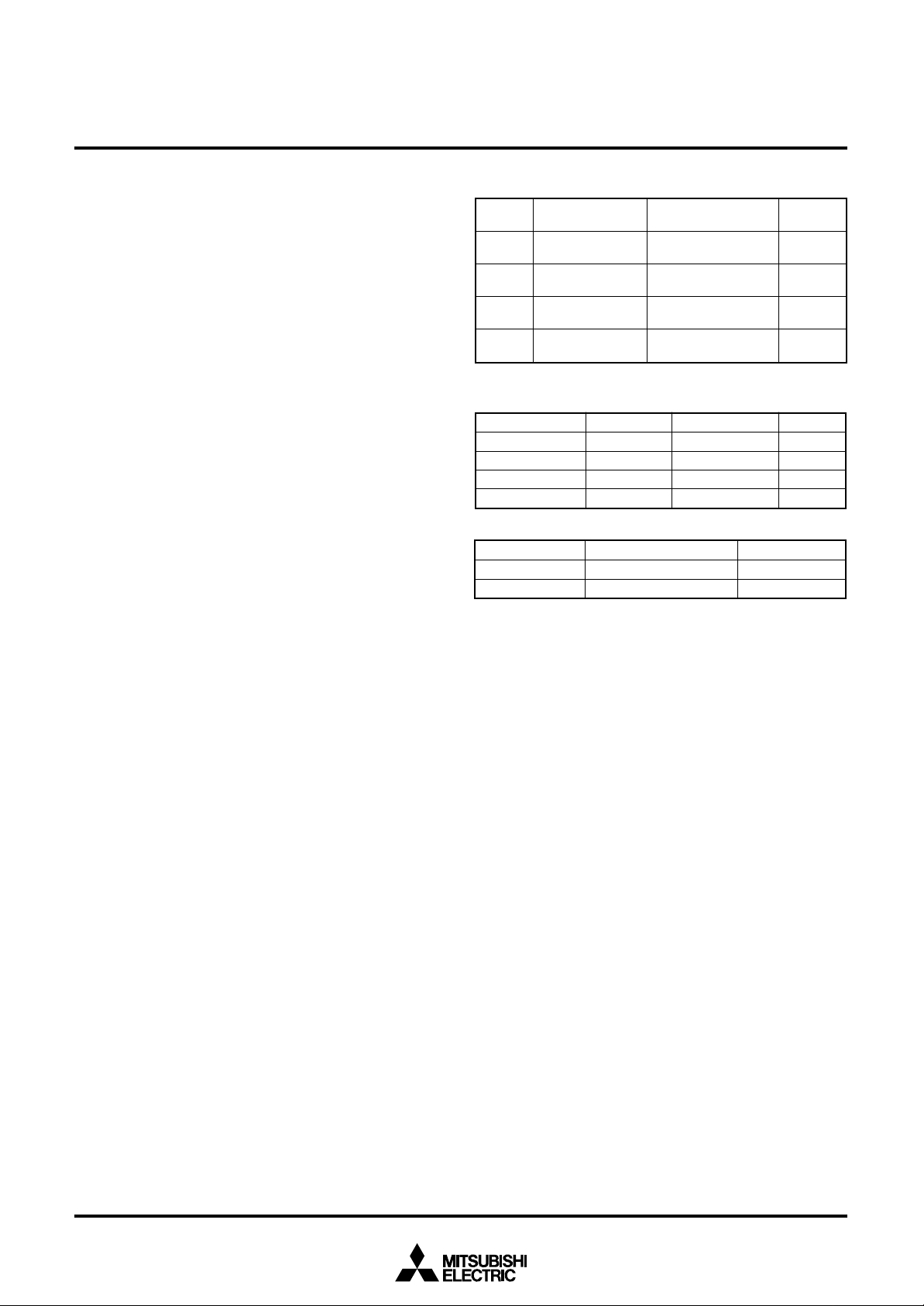
Product
M34501M2-XXXFP
M34501M4-XXXFP
M34501E4FP (Note)
Note: Shipped in blank.
ROM (PROM) size
(✕ 10 bits)
2048 words
4096 words
4096 words
●Timers
Timer 1...................................... 8-bit timer with a reload register
Timer 2...................................... 8-bit timer with a reload register
●Interrupt ........................................................................ 4 sources
●Key-on wakeup function pins ................................................... 12
●Input/Output port ......................................................................14
●A-D converter .................. 10-bit successive comparison method
●Watchdog timer
●Clock generating circuit (ceramic resonator/RC oscillation)
●LED drive directly enabled (port D)
●Power-on reset circuit
●Voltage drop detection circuit ........................... VRST: Typ. 3.5 V
(Ta = 25 °C)
APPLICATION
Electrical household appliance, consumer electronic products, office automation equipment, etc.
RAM size
(✕ 4 bits)
128 words
256 words
256 words
Package
20P2N-A
20P2N-A
20P2N-A
ROM type
Mask ROM
Mask ROM
One Time PROM
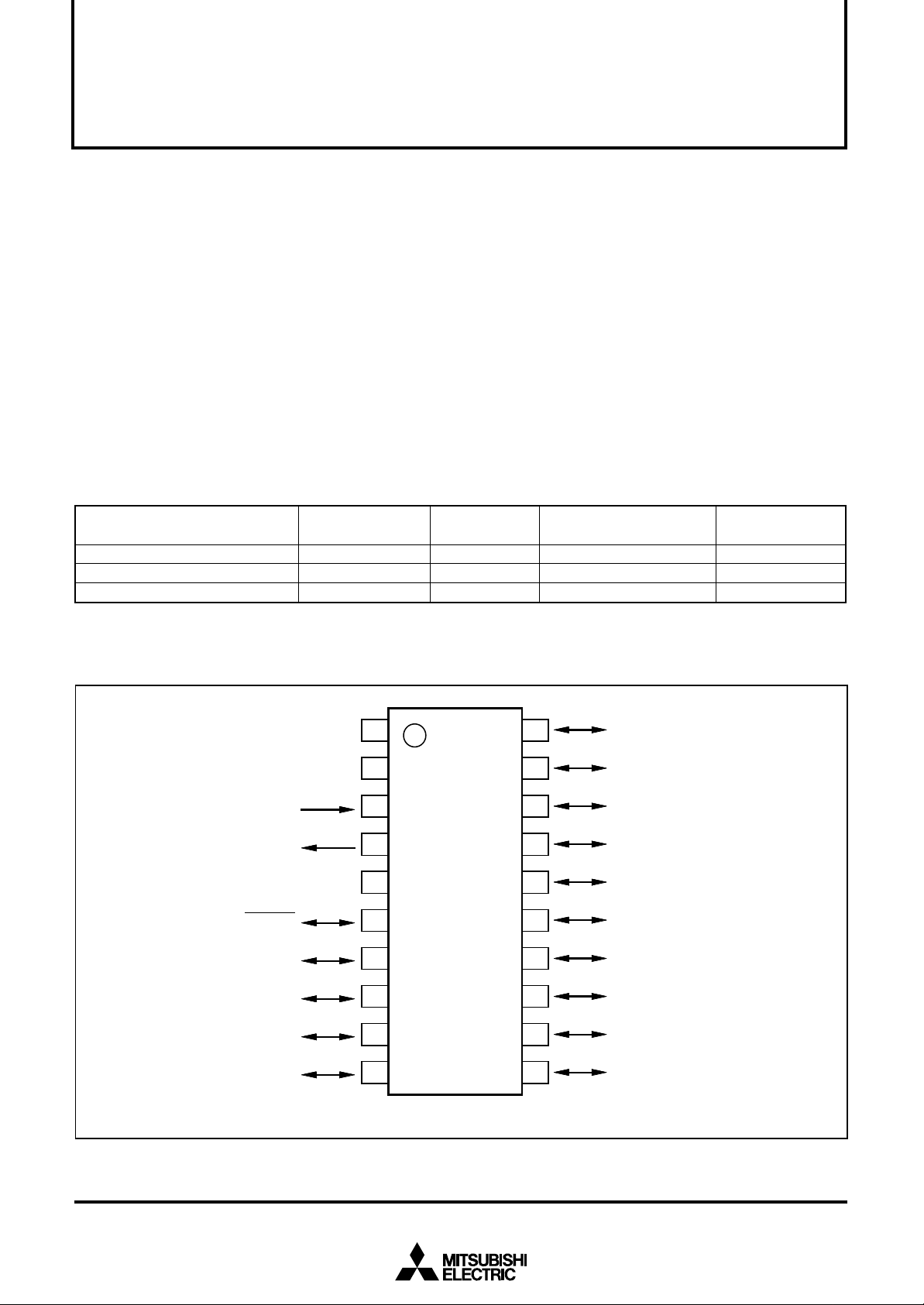
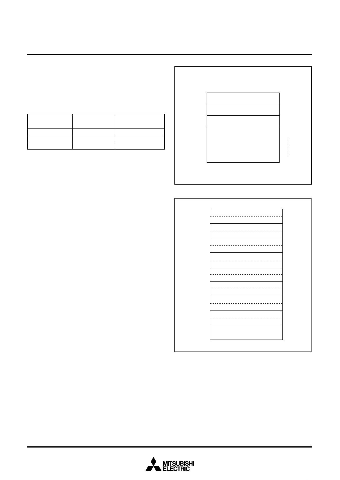
PIN CONFIGURATION
P 21/ A
P 20/ A
V
D D
V
S S
X
I N
X
O U T
C N V
S S
R E S E T
I N 1
I N 0
D3/ K
D
2
/ C
1
2
3
4
5
6
7
8
9
1 0
M
P
M
P
P0
2 0
3 4 5 0 1 M x - X X X F
3 4 5 0 1 E 4 F
1 9
1 8
1 7
1 6
1 5
1 4
1 3
1 2
1 1
0
P0
1
P0
2
P0
3
P1
0
P1
1
P12/CNTR
3
/INT
P1
D
0
D
1
Pin configuration (top view) (4501 Group)
O u t l i n e 2 0 P 2 N - A
Page 2
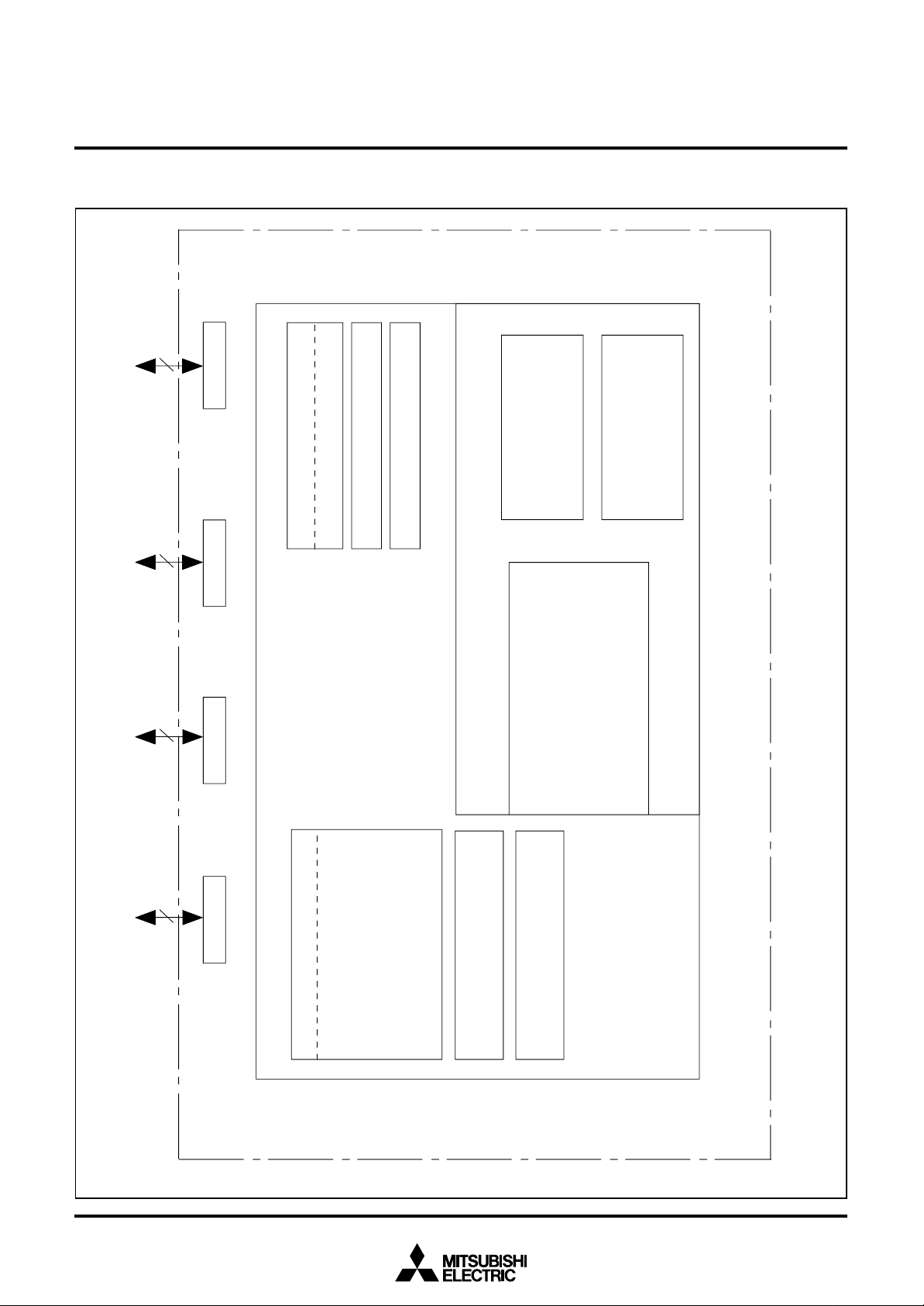
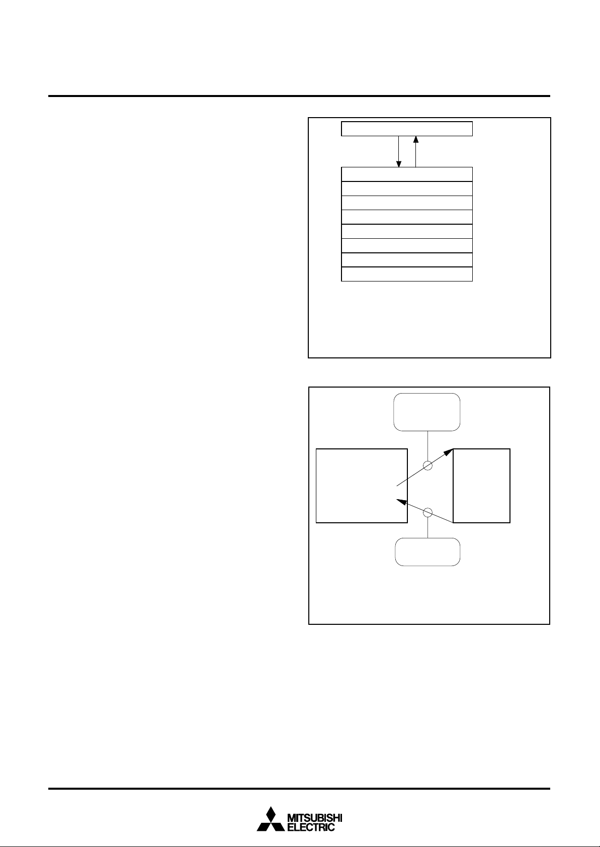
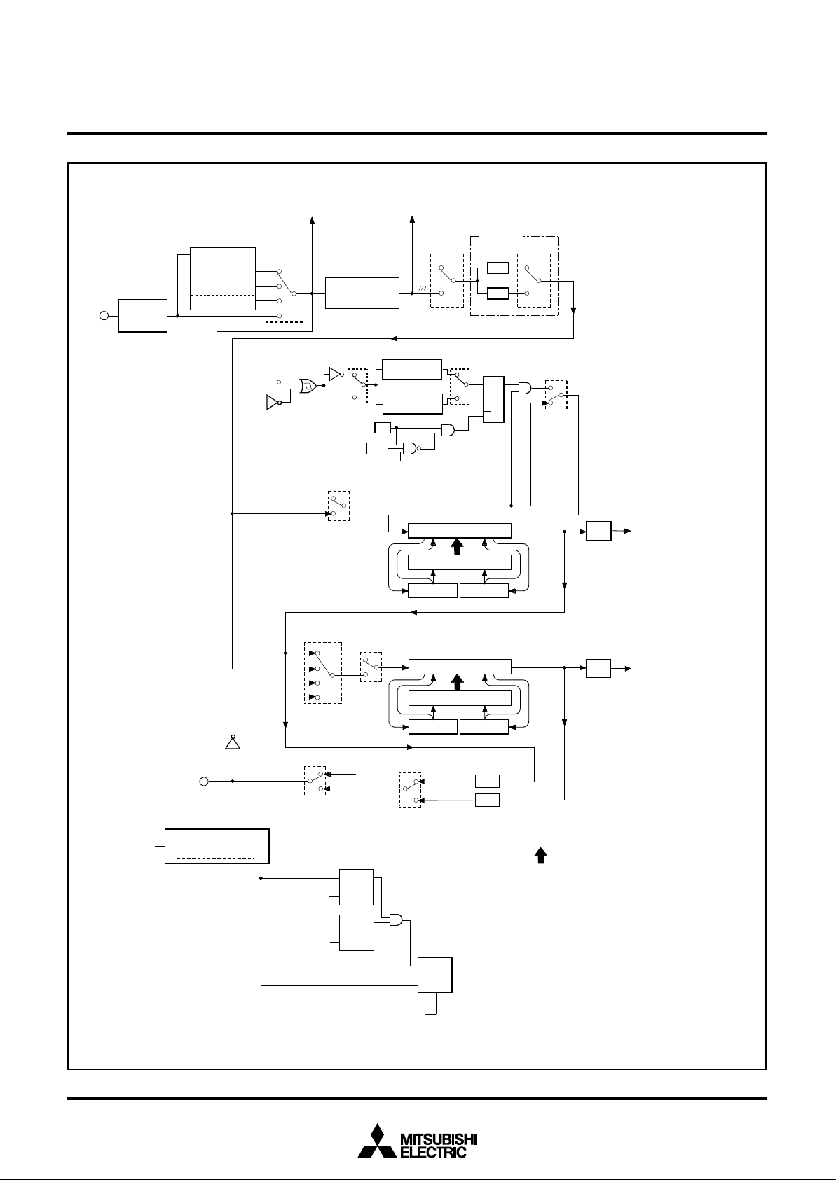
BLOCK DIAGRAM
R
A
M
R
O
M
e m o r
y
/
O
p
o
r
t
I
n t e r n a l p e r i p h e r a l f u n c t i o n
s
T
i m e
r
T
i
m
e
r
1
(
8
b
i
t
s
)
S
y
s
t
e
m
c
l
o
c
k
g
e
n
e
r
a
t
i
n
g
c
i
r
c
u
i
t
T
i
m
e
r
2
(
8
b
i
t
s
)
1
2 8 , 2 5 6 w o r d s
✕
4 b i t
s
2
0
4
8
,
4
0
9
6
w
o
r
d
s
✕
1
0
b
i
t
s
4
5 0 0 S e r i e
s
C
P U c o r
e
R
e g i s t e r B ( 4 b i t s
)
R
e g i s t e r A ( 4 b i t s
)
R
e
g
i
s
t
e
r
D
(
3
b
i
t
s
)
R
e g i s t e r E ( 8 b i t s
)
S
t a c k r e g i s t e r S K ( 8 l e v e l s
)
I
n t e r r u p t s t a c k r e g i s t e r S D P ( 1 l e v e l
)
A
L U ( 4 b i t s
)
I
N
-
X
O
U
T
W
a t c h d o g t i m e
r
(
1 6 b i t s
)
(
1 0 b i t s
✕
2
c
h
)
A
-
D
c
o
n
v
e
r
t
e
r
o
r
t
P
0
4
P
o r t P
1
4
P
o r t P
2
o
r
t
D
4
P
o
w
e
r
-
o
n
r
e
s
e
t
c
i
r
c
u
i
t
V
o
l
t
a
g
e
d
r
o
p
d
e
t
e
c
t
i
o
n
c
i
r
c
u
i
t
MITSUBISHI MICROCOMPUTERS
4501 Group
SINGLE-CHIP 4-BIT CMOS MICROCOMPUTER
Block diagram (4501 Group)
2
Page 3
PERFORMANCE OVERVIEW
Parameter
Number of basic instructions
Minimum instruction execution time
Memory sizes
Input/Output
ports
Timers
A-D converter
Interrupt
Subroutine nesting
Device structure
Package
Operating temperature range
Supply voltage
Power
dissipation
(typical value)
ROM
RAM
D0–D3
P00–P03
P10–P13
P20, P21
C
K
CNTR
INT
AIN0, AIN1
Timer 1
Timer 2
Analog input
Sources
Nesting
Active mode
RAM back-up mode
M34501M2
M34501M4/E4
M34501M2
M34501M4/E4
I/O
I/O
I/O
I/O
I/O
I/O
Timer I/O
Interrupt input
Analog input
MITSUBISHI MICROCOMPUTERS
4501 Group
SINGLE-CHIP 4-BIT CMOS MICROCOMPUTER
Function
111
0.68 µs (at 4.4 MHz oscillation frequency, in high-speed mode)
2048 words ✕ 10 bits
4096 words ✕ 10 bits
128 words ✕ 4 bits
256 words ✕ 4 bits
Four independent I/O ports.
Input is examined by skip decision.
Ports D2 and D3 are equipped with a pull-up function and a key-on wakeup function. Both functions can be switched by software.
Ports D2 and D3 are also used as ports C and K, respectively.
4-bit I/O port; each pin is equipped with a pull-up function and a key-on wakeup function. Both
functions can be switched by software.
4-bit I/O port; each pin is equipped with a pull-up function and a key-on wakeup function. Both
functions can be switched by software.
Ports P12 and P13 are also used as CNTR and INT, respectively.
2-bit I/O port; each pin is equipped with a pull-up function and a key-on wakeup function. Both
functions can be switched by software.
Ports P20 and P21 are also used as AIN0 and AIN1, respectively.
1-bit I/O; Port C is also used as port D2.
1-bit I/O; Port K is also used as port D3.
1-bit I/O; CNTR pin is also used as port P12.
1-bit input; INT pin is also used as port P13.
Two independent I/O ports. AIN0–AIN1 is also used as ports P20, P21, respectively.
8-bit programmable timer with a reload register.
8-bit programmable timer with a reload register and has a event counter.
10-bit wide, This is equipped with an 8-bit comparator function.
2 channel (AIN0 pin, AIN1 pin)
4 (one for external, two for timer, one for A-D)
1 level
8 levels
CMOS silicon gate
20-pin plastic molded SOP (20P2N-A)
–20 °C to 85 °C
VRST to 5.5 V (VRST: detected voltage of voltage drop detection circuit. Refer to the voltage
drop detection circuit characteristics.)
1.7 mA (at VDD = 5.0 V, 4.0 MHz oscillation frequency, in high-speed mode, output transistors
in the cut-off state)
0.1 µA (at room temperature, VDD = 5 V, output transistors in the cut-off state)
3
Page 4
PIN DESCRIPTION
Pin
VDD
VSS
CNVSS
RESET
XIN
XOUT System clock output Output
D0–D3
P00–P03
P10–P13
P20, P21
Port C
Port K
CNTR
INT
AIN0–AIN1
Name
Power supply
Ground
CNVSS
Reset input/output
System clock input
I/O port D
I/O
I/O port P1
I/O port P2
I/O port C
I/O port K
Timer input/output
Interrupt input
Analog input
Input/Output
—
—
—
I/O
Input
I/O
I/O
I/O
I/O
I/O
I/O
I/O
Input
Input
MITSUBISHI MICROCOMPUTERS
4501 Group
SINGLE-CHIP 4-BIT CMOS MICROCOMPUTER
Function
Connected to a plus power supply.
Connected to a 0 V power supply.
Connect CNVSS to VSS and apply “L” (0V) to CNVSS certainly.
An N-channel open-drain I/O pin for a system reset. When the watchdog timer or the
voltage drop detection circuit cause the system to be reset, the RESET pin outputs
“L” level.
I/O pins of the system clock generating circuit. When using a ceramic resonator, connect
it between pins XIN and XOUT. A feedback resistor is built-in between them. When using
the RC oscillation, connect a resistor and a capacitor to XIN, and leave XOUT pin open.
Each pin of port D has an independent 1-bit wide I/O function. Each pin has an output latch. For input use, set the latch of the specified bit to “1.” Input is examined by
skip decision. The output structure is N-channel open-drain. Ports D2 and D3 are
equipped with a pull-up function and a key-on wakeup function. Both functions can
be switched by software.
Ports D2 and D3 are also used as ports C and K, respectively.
Port P0 serves as a 4-bit I/O port, and it can be used as inputs when the output latch
is set to “1.” The output structure is N-channel open-drain. Port P0 has a key-on
wakeup function and a pull-up function. Both functions can be switched by software.
Port P1 serves as a 4-bit I/O port, and it can be used as inputs when the output latch
is set to “1.” The output structure is N-channel open-drain. Port P1 has a key-on
wakeup function and a pull-up function. Both functions can be switched by software.
Ports P12 and P13 are also used as CNTR and INT, respectively.
Port P2 serves as a 2-bit I/O port, and it can be used as inputs when the output latch
is set to “1.” The output structure is N-channel open-drain. Port P2 has a key-on
wakeup function and a pull-up function. Both functions can be switched by software.
Ports P20 and P21 are also used as AIN0 and AIN1, respectively.
1-bit I/O port. Port C can be used as inputs when the output latch is set to “1.” The
output structure is N-channel open-drain. Port C has a key-on wakeup function and
a pull-up function. Both functions can be switched by software. Port C is also used
as port D2.
1-bit I/O port. Port K can be used as inputs when the output latch is set to “1.” The
output structure is N-channel open-drain. Port K has a key-on wakeup function and
a pull-up function. Both functions can be switched by software. Port K is also used
as port D3.
CNTR pin has the function to input the clock for the timer 2 event counter, and to output the timer 1 or timer 2 underflow signal divided by 2. This pin is also used as port
P12.
INT pin accepts external interrupts. It has the key-on wakeup function which can be
switched by software. This pin is also used as port P13.
A-D converter analog input pins. AIN0 and AIN1 are also used as ports P20 and P21,
respectively.
MULTIFUNCTION
Pin
D2
D3
P12
P13
Notes 1: Pins except above have just single function.
2: The input/output of D
3: The input of P1
4: The input/output of P2
4
Multifunction
C
K
CNTR
INT
2, D3, P12 and P13 can be used even when C, K, INT and CNTR (input) are selected.
2 can be used even when CNTR (output) is selected.
0, P21 can be used even when AIN0, AIN1 are selected.
Pin
C
K
CNTR
INT
Multifunction
D2
D3
P12
P13
P20
P21
Pin
Multifunction
AIN0
AIN1
AIN0
AIN1
Pin
Multifunction
P20
P21
Page 5
DEFINITION OF CLOCK AND CYCLE
MITSUBISHI MICROCOMPUTERS
4501 Group
SINGLE-CHIP 4-BIT CMOS MICROCOMPUTER
● Operation source clock
The operation source clock is the source clock to operate this
product. In this product, the following clocks are used.
• External ceramic resonator
• External RC oscillation
• Clock (f(X
• Clock (f(RING)) of the ring oscillator which is the internal oscil-
lator.
● System clock
The system clock is the basic clock for controlling this product.
The system clock is selected by the bits 2 and 3 of the clock control register MR.
Table Selection of system clock
Register MR System clock
MR3
0
0
1
1
Notes 1: The ring oscillator clock is f(RING), the clock by the ce-
IN)) by the external clock
Operation mode
MR2
0
1
0
1
ramic resonator, RC oscillation or external clock is f(XIN).
2: The default mode is selected after system is released
from reset and is returned from RAM back-up.
(Note 1)
f(XIN) or f(RING)
f(XIN)/2 or f(RING)/2
f(XIN)/4 or f(RING)/4
f(XIN)/8 or f(RING)/8
High-speed mode
Middle-speed mode
Low-speed mode
Default mode
● Instruction clock
The instruction clock is a signal derived by dividing the system
clock by 3. The one instruction clock cycle generates the one
machine cycle.
● Machine cycle
The machine cycle is the standard cycle required to execute the
instruction.
PORT FUNCTION
Port
Port D
Port P0
Port P1
Port P2
D0, D1
D2/C
D3/K
P00–P03
P10, P11
P12/CNTR,
P13/INT
P20/AIN0
P21/AIN1
Input
Output
I/O
(4)
I/O
(4)
I/O
(4)
I/O
(2)
Output structure
N-channel open-drain
N-channel open-drain
N-channel open-drain
N-channel open-drain
I/O
unit
1
4
4
2
Control
instructions
SD, RD
SZD, CLD
SCP, RCP
SNZCP
IAK, OKA
OP0A
IAP0
OP1A
IAP1
OP2A
IAP2
Control
registers
PU2, K2
PU0, K0
PU1, K1
W6, I1
PU2, K2
Q1
RemarkPin
Built-in programmable pull-up
functions
Key-on wakeup functions
(programmable)
Built-in programmable pull-up
functions
Key-on wakeup functions
(programmable)
Built-in programmable pull-up
functions
Key-on wakeup functions
(programmable)
Built-in programmable pull-up
functions
Key-on wakeup functions
(programmable)
5
Page 6
MITSUBISHI MICROCOMPUTERS
4501 Group
SINGLE-CHIP 4-BIT CMOS MICROCOMPUTER
CONNECTIONS OF UNUSED PINS
Connection
System operates by the ring oscillator. (Note 1)
System operates by the external clock.
XIN
XOUT
Pin
Connect to VSS.
Open.
(The ceramic resonator is selected with the CMCK instruction.)
System operates by the RC oscillator.
(The RC oscillation is selected with the CRCK instruction.)
System operates by the ring oscillator. (Note 1)
D0, D1
Open. (Output latch is set to “1.”)
Open. (Output latch is set to “0.”)
Connect to VSS.
D2/C
D3/K
P00–P03
P10, P11
P12/CNTR
P13/INT
Open. (Output latch is set to “1.”)
Open. (Output latch is set to “0.”)
Connect to VSS.
Open. (Output latch is set to “1.”)
Open. (Output latch is set to “0.”)
Connect to VSS.
Open. (Output latch is set to “1.”)
Open. (Output latch is set to “0.”)
Connect to VSS.
Open. (Output latch is set to “1.”)
The key-on wakeup function is not selected. (Note 4)
The pull-up function and the key-on wakeup function are not selected. (Notes 2, 3)
The pull-up function and the key-on wakeup function are not selected. (Notes 2, 3)
The key-on wakeup function is not selected. (Note 4)
The pull-up function and the key-on wakeup function are not selected. (Notes 2, 3)
The pull-up function and the key-on wakeup function are not selected. (Notes 2, 3)
The key-on wakeup function is not selected. (Note 4)
The pull-up function and the key-on wakeup function are not selected. (Notes 2, 3)
The pull-up function and the key-on wakeup function are not selected. (Notes 2, 3)
The key-on wakeup function is not selected. The input to INT pin is disabled.
(Notes 4, 5)
Open. (Output latch is set to “0.”)
Connect to VSS.
P20/AIN0
P21/AIN1
Open. (Output latch is set to “1.”)
Open. (Output latch is set to “0.”)
Connect to VSS.
Notes 1: When the ceramic resonator or the RC oscillation is not selected by program, system operates by the ring oscillator (internal oscillator).
2: When the pull-up function is left valid, the supply current is increased. Do not select the pull-up function.
3: When the key-on wakeup function is left valid, the system returns from the RAM back-up state immediately after going into the RAM back-up state.
Do not select the key-on wakeup function.
4: When selecting the key-on wakeup function, select also the pull-up function.
5: Clear the bit 3 (I1
3) of register I1 to “0” to disable to input to INT pin (after reset: I13 = “0”)
The pull-up function and the key-on wakeup function are not selected. (Notes 2, 3)
The pull-up function and the key-on wakeup function are not selected. (Notes 2, 3)
The key-on wakeup function is not selected. (Note 4)
The pull-up function and the key-on wakeup function are not selected. (Notes 2, 3)
The pull-up function and the key-on wakeup function are not selected. (Notes 2, 3)
Usage condition
(Note when connecting to V
● Connect the unused pins to V
SS and VDD)
SS and VDD using the thickest wire at the shortest distance against noise.
6
Page 7
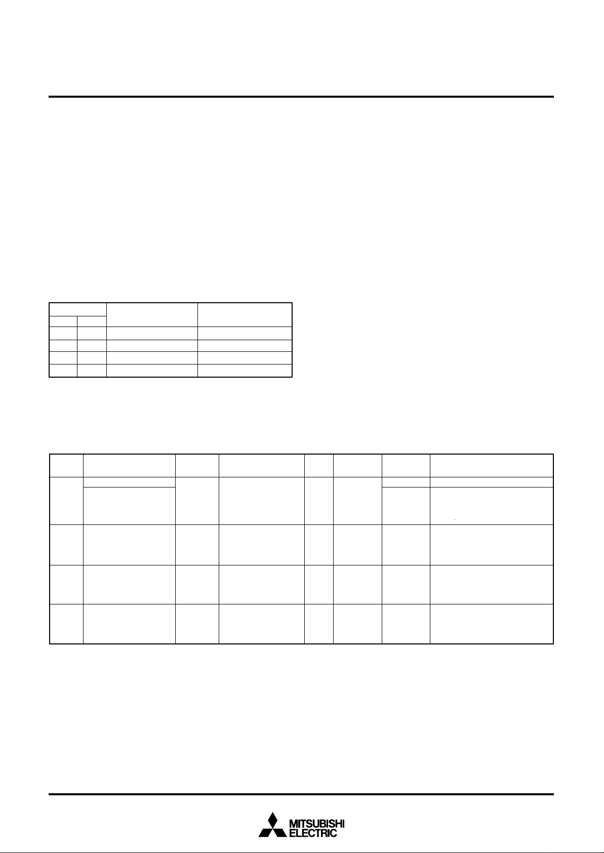
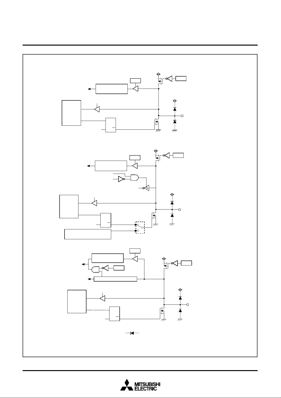
PORT BLOCK DIAGRAMS
R e g i s t e r Y
SD instruction
R D i n s t r u c t i o n
D e c o d e rR e g i s t e r Y
D e c o d e r
CLD
instruction
Key-on wakeup
Skip decision
(SZD instruction)
S
RQ
“L” level
detection circuit
MITSUBISHI MICROCOMPUTERS
4501 Group
SINGLE-CHIP 4-BIT CMOS MICROCOMPUTER
D0, D
1
(Note 1)
Pull-up
transistor
PU2
K2
2
2
SD instruction
R D i n s t r u c t i o n
SD instruction
R D i n s t r u c t i o n
C L D
i n s t r u c t i o n
SCP instruction
RCP instruction
DecoderRegister Y
K e y - o n w a k e u p
C L D
i n s t r u c t i o n
Skip decision
(SZD instruction)
Skip decision
S
(SNZCP
instruction)
(Note 1)
D2/ C
( N o t e 2 )
RQ
S
RQ
Pull-up
transistor
PU2
3
K 2
3
“L” level
detection circuit
Skip decision
(SZD instruction)
IAK instruction
S
Register A
(Note 1)
D3/K
( N o t e 2 )
RQ
A
0
D
Port block diagram (1)
O K A i n s t r u c t i o n
TQ
N o t e s 1 :
This symbol represents a parasitic diode on the port.
2: Applied potential to ports D
2
/C and D3/K must be VDD or less.
7
Page 8
R e g i s t e r A
A
( N o t e 2 )
I A P 0 i n s t r u c t i o n
i
MITSUBISHI MICROCOMPUTERS
4501 Group
SINGLE-CHIP 4-BIT CMOS MICROCOMPUTER
P u l l - u p t r a n s i s t o r
( N o t e 2 )
PU0
i
( N o t e 1 )
i
A
O P 0 A i n s t r u c t i o n
K e y - o n w a k e u p i n p u t
R e g i s t e r A
A
j
( N o t e 3 )
A
j
O P 0 A i n s t r u c t i o n
K e y - o n w a k e u p
“L ” l e v e l
d e t e c t i o n c i r c u i t
IAP0 instruction
“L” level detection
D
Q
T
D
Q
T
circuit
K0
K0
P 00, P 0
i
P u l l - u p t r a n s i s t o r
( N o t e 3 )
PU0
j
( N o t e 4 )
1
( N o t e 1 )
P 02, P 0
j
(Note 4)
3
Port block diagram (2)
8
Notes 1:
T h i s s y m b o l r e p r e s e n t s a p a r a s i t i c d i o d e o n t h e p o r t .
2 : i r e p r e s e n t s 0 o r 1 .
3 : j r e p r e s e n t s 2 o r 3 .
4 : A p p l i e d p o t e n t i a l t o p o r t P 0 m u s t b e V
D D
o r l e s s .
Page 9
K e y - o n w a k e u p i n p u t
“L” level
detection circuit
K1
i
Pull-up transistor
( N o t e 2 )
MITSUBISHI MICROCOMPUTERS
4501 Group
SINGLE-CHIP 4-BIT CMOS MICROCOMPUTER
PU1
i
(Note 2)
Register A
Ai
( N o t e 2 )
A i
O P 1 A i n s t r u c t i o n
K e y - o n w a k e u p i n p u t
Clock input for timer 2 event counter
R e g i s t e r A
A
2
A
2
OP1A instruction
T i m e r 1 o r t i m e r 2 u n d e r f l o w
s i g n a l d i v i d e d b y 2
I A P 1 i n s t r u c t i o n
“ L ” l e v e l
d e t e c t i o n c i r c u i t
IAP1 instruction
D
TQ
D
TQ
W 2
1
W 2
0
K1
2
W6
( N o t e 1 )
P10, P1
1
(Note 3)
Pull-up transistor
PU1
2
(Note 1)
P 12/ C N T R ( N o t e 3 )
0
0
1
Key-on wakeup input
E x t e r n a l 0 i n t e r r u p tE x t e r n a l i n t e r r u p t c i r c u i t
Port block diagram (3)
R e g i s t e r A
A
A
O P 1 A i n s t r u c t i o n
d e t e c t i o n c i r c u i t
I A P 1 i n s t r u c t i o n
3
3
“ L ” l e v e l
D
T
K1
3
K 1
3
Q
N o t e s 1 :
T h i s s y m b o l r e p r e s e n t s a p a r a s i t i c d i o d e o n t h e p o r t .
2 : i r e p r e s e n t s 0 o r 1 .
3 : A p p l i e d p o t e n t i a l t o p o r t P 1 m u s t b e V
P u l l - u p t r a n s i s t o r
PU1
3
(Note 1)
D D
P13/INT (Note 3)
o r l e s s .
9
Page 10
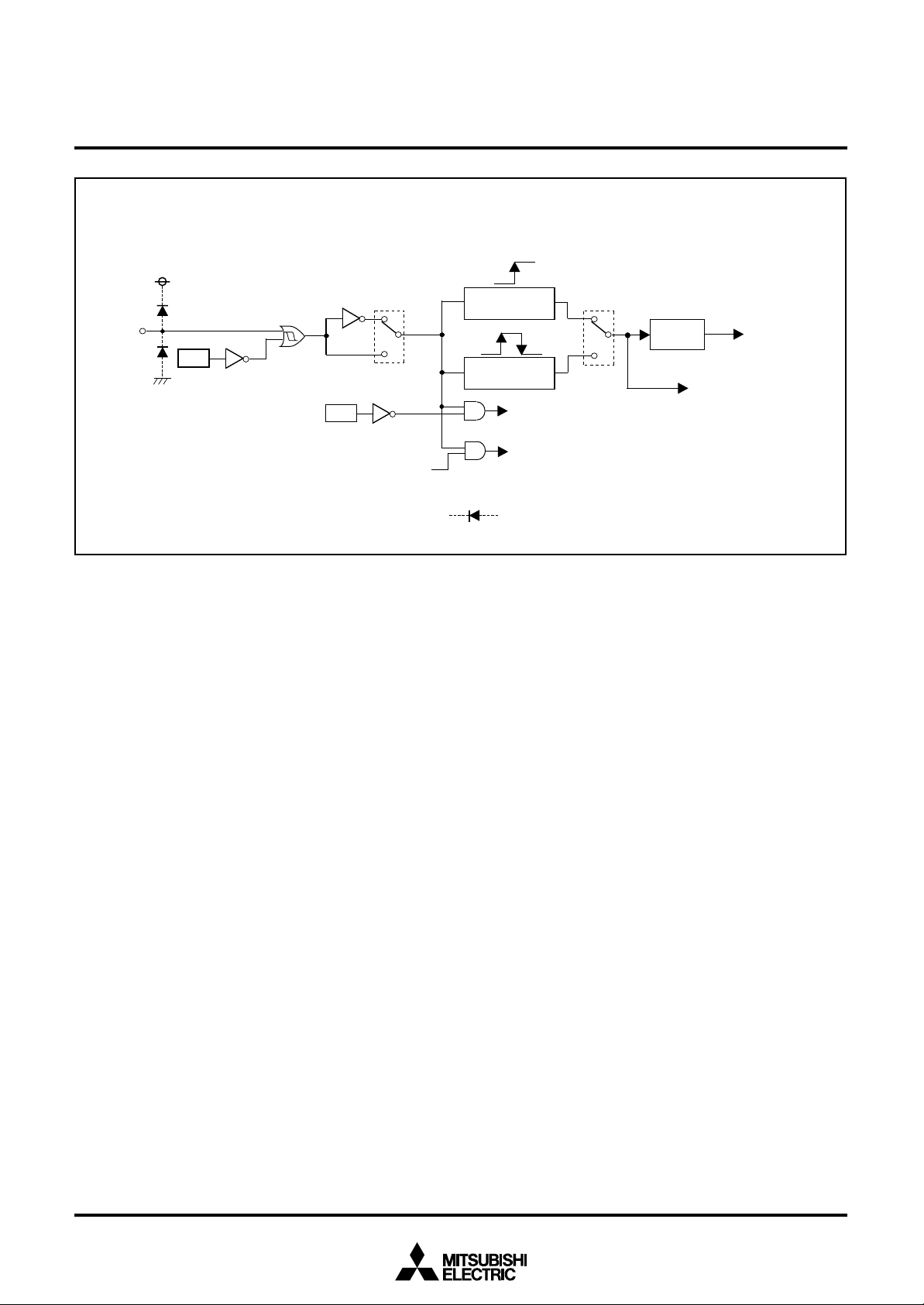
K e y - o n w a k e u p i n p u t
R e g i s t e r A
A
0
A
0
O P 2 A i n s t r u c t i o n
d e t e c t i o n c i r c u i t
I A P 2 i n s t r u c t i o n
A n a l o g i n p u t
“ L ” l e v e l
D
T
Q
K 2
0
Q 1
D e c o d e r
SINGLE-CHIP 4-BIT CMOS MICROCOMPUTER
Pull-up transistor
PU2
( N o t e 1 )
MITSUBISHI MICROCOMPUTERS
4501 Group
0
I N 0
(Note 3)
P 20/ A
K e y - o n w a k e u p i n p u t
R e g i s t e r A
Port block diagram (4)
I A P 2 i n s t r u c t i o n
A
1
A
1
O P 2 A i n s t r u c t i o n
Analog input
K 2
1
Pull-up transistor
“ L ” l e v e l
d e t e c t i o n c i r c u i t
D
Q
T
Q1
Decoder
N o t e s 1 :
T h i s s y m b o l r e p r e s e n t s a p a r a s i t i c d i o d e o n t h e p o r t .
2 : i r e p r e s e n t s 0 o r 1 .
3 : A p p l i e d p o t e n t i a l t o p o r t s P 2 a n d P 3 m u s t b e V
PU2
( N o t e 1 )
1
P 21/ A
I N 1
D D
o r l e s s .
( N o t e 3 )
10
Page 11
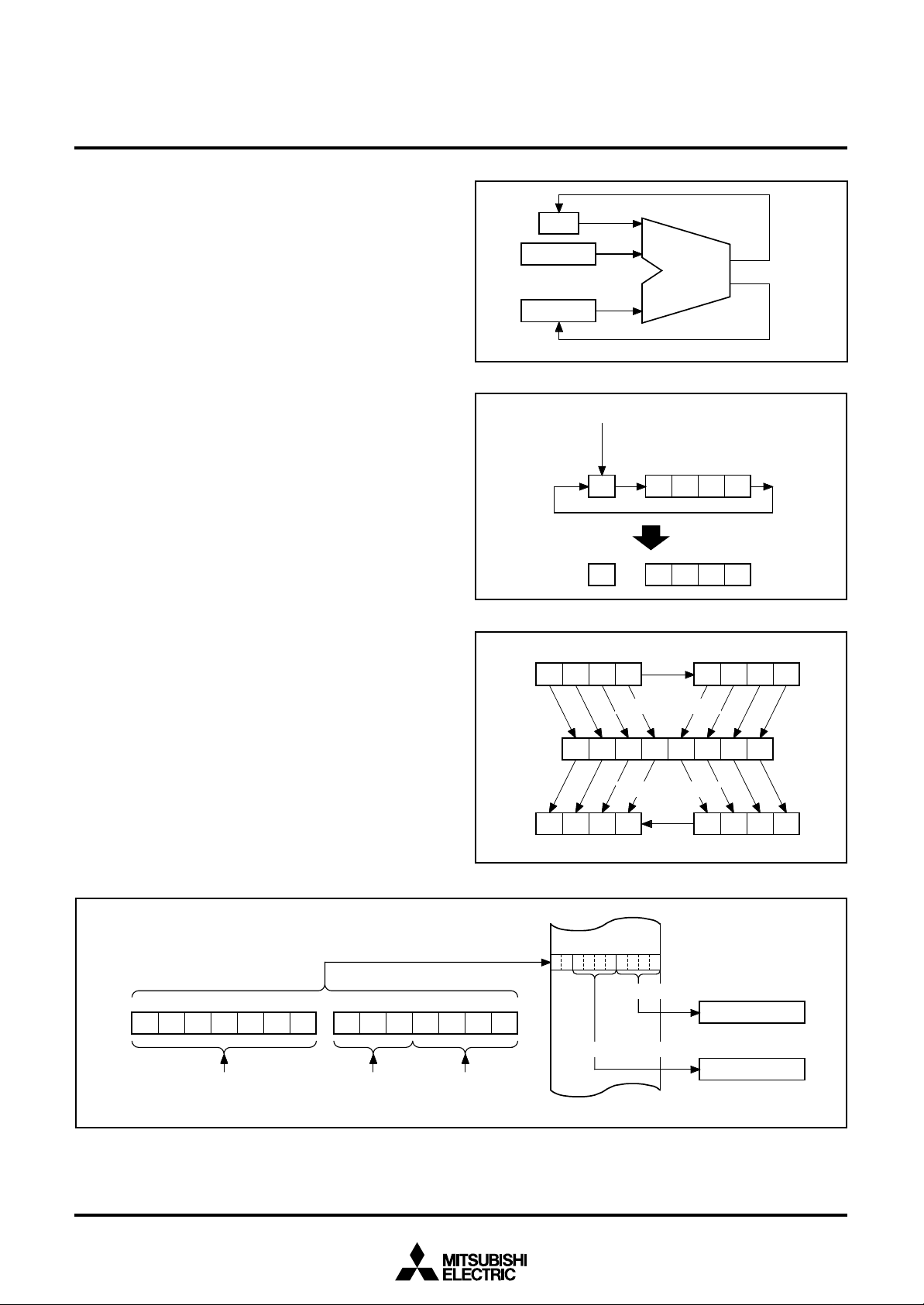
P1
( N o t e )
3
/INT
MITSUBISHI MICROCOMPUTERS
4501 Group
SINGLE-CHIP 4-BIT CMOS MICROCOMPUTER
I1
2
F a l l i n g
0
I 1
3
1
R i s i n g
K 1
3
O n e - s i d e d e d g e
d e t e c t i o n c i r c u i t
B o t h e d g e s
d e t e c t i o n c i r c u i t
Wakeup
I 1
1
0
E X F 0
1
E x t e r n a l 0
i n t e r r u p t
Timer 1 count start
synchronization
circuit input
External interrupt circuit structure
S N Z I 0 i n s t r u c t i o n
Skip
•
This symbol represents a parasitic diode on the port.
11
Page 12
MITSUBISHI MICROCOMPUTERS
4501 Group
SINGLE-CHIP 4-BIT CMOS MICROCOMPUTER
FUNCTION BLOCK OPERATIONS
CPU
(1) Arithmetic logic unit (ALU)
The arithmetic logic unit ALU performs 4-bit arithmetic such as 4bit data addition, comparison, AND operation, OR operation, and
bit manipulation.
(2) Register A and carry flag
Register A is a 4-bit register used for arithmetic, transfer, exchange, and I/O operation.
Carry flag CY is a 1-bit flag that is set to “1” when there is a carry
with the AMC instruction (Figure 1).
It is unchanged with both A n instruction and AM instruction. The
value of A0 is stored in carry flag CY with the RAR instruction (Figure 2).
Carry flag CY can be set to “1” with the SC instruction and cleared
to “0” with the RC instruction.
(3) Registers B and E
Register B is a 4-bit register used for temporary storage of 4-bit
data, and for 8-bit data transfer together with register A.
Register E is an 8-bit register. It can be used for 8-bit data transfer
with register B used as the high-order 4 bits and register A as the
low-order 4 bits (Figure 3).
Register E is undefined after system is released from reset and returned from the RAM back-up. Accordingly, set the initial value.
(4) Register D
Register D is a 3-bit register.
It is used to store a 7-bit ROM address together with register A and
is used as a pointer within the specified page when the TABP p,
BLA p, or BMLA p instruction is executed (Figure 4).
Register D is undefined after system is released from reset and returned from the RAM back-up. Accordingly, set the initial value.
< C a r r y >
( C Y )
( M ( D P ) )
Addition
ALU
(A)
< R e s u l t >
Fig. 1 AMC instruction execution example
<Set>
SC instruction
< C l e a r >
R C i n s t r u c t i o n
C YA3A2A1A
<Rotation>
RAR instruction
A
0
C YA3A2A
Fig. 2 RAR instruction execution example
R e g i s t e r BR
B3B2B1B
TAB instruction
0
A3A2A1A
T E A B i n s t r u c t i o n
Register E
E7E6E5E4E3E2E1E
T A B E i n s t r u c t i o n
B3B2B1B
Register B Register A
0
TBA instruction
A3A2A1A
0
1
e g i s t e r
A
0
0
0
T A B P p i n s t r u c t i o n
PCH
p6 p5 p4 p3 p2 p1 p0
I m m e d i a t e f i e l d
v a l u e p
Fig. 4 TABP p instruction execution example
12
DR2DR1DR0
T h e c o n t e n t s o f
r e g i s t e r D
Fig. 3 Registers A, B and register E
S p e c i f y i n g a d d r e s s
PCL
A3 A2 A1 A0
The contents of
register A
ROM
840
L o w - o r d e r 4 b i t s
R e g i s t e r A ( 4 )
Middle-order 4 bits
R e g i s t e r B ( 4 )
Page 13
MITSUBISHI MICROCOMPUTERS
r
”
e
t
0
4501 Group
SINGLE-CHIP 4-BIT CMOS MICROCOMPUTER
(5) Stack registers (SKS) and stack pointer (SP)
Stack registers (SKs) are used to temporarily store the contents of
program counter (PC) just before branching until returning to the
original routine when;
• branching to an interrupt service routine (referred to as an interrupt service routine),
• performing a subroutine call, or
• executing the table reference instruction (TABP p).
Stack registers (SKs) are eight identical registers, so that subroutines can be nested up to 8 levels. However, one of stack registers
is used respectively when using an interrupt service routine and
when executing a table reference instruction. Accordingly, be careful not to over the stack when performing these operations
together. The contents of registers SKs are destroyed when 8 levels are exceeded.
The register SK nesting level is pointed automatically by 3-bit
stack pointer (SP). The contents of the stack pointer (SP) can be
transferred to register A with the TASP instruction.
Figure 5 shows the stack registers (SKs) structure.
Figure 6 shows the example of operation at subroutine call.
(6) Interrupt stack register (SDP)
Interrupt stack register (SDP) is a 1-stage register. When an interrupt occurs, this register (SDP) is used to temporarily store the
contents of data pointer, carry flag, skip flag, register A, and register B just before an interrupt until returning to the original routine.
Unlike the stack registers (SKs), this register (SDP) is not used
when executing the subroutine call instruction and the table reference instruction.
(7) Skip flag
Skip flag controls skip decision for the conditional skip instructions
and continuous described skip instructions. When an interrupt occurs, the contents of skip flag is stored automatically in the interrupt
stack register (SDP) and the skip condition is retained.
Program counter (PC)
S K
S K
S K
S K
S K
S K
S K
SK
0
1
2
3
4
5
6
7
E x e c u t i n g R T
i n s t r u c t i o n
Executing BM
instruction
Stack pointer (SP) points “7” at reset o
returning from RAM back-up mode. It points “0
by executing the first BM instruction, and th
contents of program counter is stored in SK0.
When the BM instruction is executed after eigh
stack registers are used ((SP) = 7), (SP) =
and the contents of SK0 is destroyed.
Fig. 5 Stack registers (SKs) structure
(SP) ← 0
(SK
0
Main program
A d d r e s s
N O
0 0 0 0
1
6
16 BM SUB1
0001
) ← 0001
(PC) ← SUB1
P
16
Subroutine
S U B 1 :
000216 NOP
( S P ) = 0
( S P ) = 1
( S P ) = 2
( S P ) = 3
( S P ) = 4
( S P ) = 5
( S P ) = 6
(SP) = 7
NOP
·
·
·
RT
( P C ) ← ( S K0)
( S P ) ← 7
Note :
Returning to the BM instruction execution
address with the RT instruction, and the BM
instruction becomes the NOP instruction.
Fig. 6 Example of operation at subroutine call
13
Page 14
MITSUBISHI MICROCOMPUTERS
4501 Group
SINGLE-CHIP 4-BIT CMOS MICROCOMPUTER
(8) Program counter (PC)
Program counter (PC) is used to specify a ROM address (page and
address). It determines a sequence in which instructions stored in
ROM are read. It is a binary counter that increments the number of
instruction bytes each time an instruction is executed. However,
the value changes to a specified address when branch instructions,
subroutine call instructions, return instructions, or the table reference instruction (TABP p) is executed.
Program counter consists of PCH (most significant bit to bit 7)
which specifies to a ROM page and PCL (bits 6 to 0) which specifies an address within a page. After it reaches the last address
(address 127) of a page, it specifies address 0 of the next page
(Figure 7).
Make sure that the PCH does not specify after the last page of the
built-in ROM.
(9) Data pointer (DP)
Data pointer (DP) is used to specify a RAM address and consists
of registers Z, X, and Y. Register Z specifies a RAM file group, register X specifies a file, and register Y specifies a RAM digit (Figure
8).
Register Y is also used to specify the port D bit position.
When using port D, set the port D bit position to register Y certainly
and execute the SD, RD, or SZD instruction (Figure 9).
• Note
Register Z of data pointer is undefined after system is released
from reset.
Also, registers Z, X and Y are undefined in the RAM back-up. After
system is returned from the RAM back-up, set these registers.
P r o g r a m c o u n t e r
p5p4p3p2p1p0a6a5a4a3a2a1a
p
6
P C
H
S p e c i f y i n g p a g e
Fig. 7 Program counter (PC) structure
S p e c i f y i n g a d d r e s s
D a t a p o i n t e r ( D P )
Z1Z0X3X2X1X0Y3Y2Y1Y
Register Y (4)
R e g i s t e r X ( 4 )
Register Z (2)
Fig. 8 Data pointer (DP) structure
S p e c i f y i n g R A M f i l e
Specifying RAM file group
Specifying bit position
P C
L
S p e c i f y i n g
R A M d i g i t
Set
0
0
D
2
D
3
0 01
0
Register Y (4)
Fig. 9 SD instruction execution example
Port D output latch
D1D
1
0
14
Page 15
PROGRAM MEMOY (ROM)
6
The program memory is a mask ROM. 1 word of ROM is composed
of 10 bits. ROM is separated every 128 words by the unit of page
(addresses 0 to 127). Table 1 shows the ROM size and pages. Figure 10 shows the ROM map of M34501M4.
Table 1 ROM size and pages
Product
M34501M2
M34501M4
M34501E4
A part of page 1 (addresses 008016 to 00FF16) is reserved for interrupt addresses (Figure 11). When an interrupt occurs, the
address (interrupt address) corresponding to each interrupt is set
in the program counter, and the instruction at the interrupt address
is executed. When using an interrupt service routine, write the instruction generating the branch to that routine at an interrupt
address.
Page 2 (addresses 010016 to 017F16) is the special page for subroutine calls. Subroutines written in this page can be called from
any page with the 1-word instruction (BM). Subroutines extending
from page 2 to another page can also be called with the BM instruction when it starts on page 2.
ROM pattern (bits 7 to 0) of all addresses can be used as data areas with the TABP p instruction.
ROM (PROM) size
(✕ 10 bits)
2048 words
4096 words
4096 words
Pages
16 (0 to 15)
32 (0 to 31)
32 (0 to 31)
MITSUBISHI MICROCOMPUTERS
SINGLE-CHIP 4-BIT CMOS MICROCOMPUTER
9
1 6
0 0 0 0
0 0 7
F1
6
0 0 8 0
1 6
0 0
F F1
0 1 0 0
0 1 7
F1
0 1 8 0
0
F F F1
Fig. 10 ROM map of M34501M4/M34501E4
0082
0084
Interrupt address page
6
1 6
S u b r o u t i n e s p e c i a l p a g e
6
1 6
9087654321
16
External 0 interrupt address0080
16
16
Timer 1 interrupt address
4501 Group
087654321
P a g e 0
P a g e 1
P a g e 2
P a g e 3
P a g e 3 1
0 0 8 6
1 6
Timer 2 interrupt address
0088
16
0 0 8 A
1 6
008C
16
008E
16
00FF
16
Fig. 11 Page 1 (addresses 008016 to 00FF16) structure
A-D interrupt address
15
Page 16
MITSUBISHI MICROCOMPUTERS
R
Z
R
X
4501 Group
SINGLE-CHIP 4-BIT CMOS MICROCOMPUTER
DATA MEMORY (RAM)
1 word of RAM is composed of 4 bits, but 1-bit manipulation (with
the SB j, RB j, and SZB j instructions) is enabled for the entire
memory area. A RAM address is specified by a data pointer. The
data pointer consists of registers Z, X, and Y. Set a value to the
data pointer certainly when executing an instruction to access
RAM.
Table 2 shows the RAM size. Figure 12 shows the RAM map.
• Note
Register Z of data pointer is undefined after system is released
from reset.
Also, registers Z, X and Y are undefined in the RAM back-up. After
system is returned from the RAM back-up, set these registers.
R A M 2 5 6 w o r d s ✕ 4 b i t s ( 1 0 2 4 b i t s )
e g i s t e r
e g i s t e r
0
23 6
1
0
1
2
3
4
5
6
Y
7
8
R
9
1 0
1 1
1 2
13
14
1 5
e g i s t e r
0
. . .
Table 2 RAM size
M34501M2
M34501M4
M34501E4
. . . . . . . .
7
Product
15
RAM size
128 words ✕ 4 bits (512 bits)
256 words ✕ 4 bits (1024 bits)
256 words ✕ 4 bits (1024 bits)
Z = 0 , X = 0 t o 1 5
Z = 0 , X = 0 t o 7
Fig. 12 RAM map
16
1 2 8 w o r d s ( 5 1 2 b i t s ) M 3 4 5 0 1 M 2
2 5 6 w o r d s ( 1 0 2 4 b i t s ) M 3 4 5 0 1 M 4 / E 4
Page 17
MITSUBISHI MICROCOMPUTERS
4501 Group
SINGLE-CHIP 4-BIT CMOS MICROCOMPUTER
INTERRUPT FUNCTION
The interrupt type is a vectored interrupt branching to an individual
address (interrupt address) according to each interrupt source. An
interrupt occurs when the following 3 conditions are satisfied.
• An interrupt activated condition is satisfied (request flag = “1”)
• Interrupt enable bit is enabled (“1”)
• Interrupt enable flag is enabled (INTE = “1”)
Table 3 shows interrupt sources. (Refer to each interrupt request
flag for details of activated conditions.)
(1) Interrupt enable flag (INTE)
The interrupt enable flag (INTE) controls whether the every interrupt enable/disable. Interrupts are enabled when INTE flag is set to
“1” with the EI instruction and disabled when INTE flag is cleared to
“0” with the DI instruction. When any interrupt occurs, the INTE flag
is automatically cleared to “0,” so that other interrupts are disabled
until the EI instruction is executed.
(2) Interrupt enable bit
Use an interrupt enable bit of interrupt control registers V1 and V2
to select the corresponding interrupt or skip instruction.
Table 4 shows the interrupt request flag, interrupt enable bit and
skip instruction.
Table 5 shows the interrupt enable bit function.
(3) Interrupt request flag
When the activated condition for each interrupt is satisfied, the corresponding interrupt request flag is set to “1.” Each interrupt
request flag is cleared to “0” when either;
• an interrupt occurs, or
• the next instruction is skipped with a skip instruction.
Each interrupt request flag is set when the activated condition is
satisfied even if the interrupt is disabled by the INTE flag or its interrupt enable bit. Once set, the interrupt request flag retains set
until a clear condition is satisfied.
Accordingly, an interrupt occurs when the interrupt disable state is
released while the interrupt request flag is set.
If more than one interrupt request flag is set when the interrupt disable state is released, the interrupt priority level is as follows
shown in Table 3.
Table 3 Interrupt sources
Priority
level
1
2
3
4
Table 4 Interrupt request flag, interrupt enable bit and skip in-
Interrupt name
External 0 interrupt
Timer 1 interrupt
Timer 2 interrupt
A-D interrupt
Table 5 Interrupt enable bit function
Interrupt enable bit
Interrupt name
External 0 interrupt
Timer 1 interrupt
Timer 2 interrupt
A-D interrupt
struction
Request flag
Occurrence of interrupt
1
0
Activated condition
Level change of INT
pin
Timer 1 underflow
Timer 2 underflow
Completion of
A-D conversion
EXF0
T1F
T2F
ADF
Enabled
Disabled
Skip instruction
SNZ0
SNZT1
SNZT2
SNZAD
Interrupt
address
Address 0
in page 1
Address 4
in page 1
Address 6
in page 1
Address C
in page 1
Enable bit
V10
V12
V13
V22
Skip instruction
Invalid
Valid
17
Page 18
MITSUBISHI MICROCOMPUTERS
4501 Group
SINGLE-CHIP 4-BIT CMOS MICROCOMPUTER
(4) Internal state during an interrupt
The internal state of the microcomputer during an interrupt is as follows (Figure 14).
• Program counter (PC)
An interrupt address is set in program counter. The address to be
executed when returning to the main routine is automatically
stored in the stack register (SK).
• Interrupt enable flag (INTE)
INTE flag is cleared to “0” so that interrupts are disabled.
• Interrupt request flag
Only the request flag for the current interrupt source is cleared to
“0.”
• Data pointer, carry flag, skip flag, registers A and B
The contents of these registers and flags are stored automatically
in the interrupt stack register (SDP).
(5) Interrupt processing
When an interrupt occurs, a program at an interrupt address is executed after branching a data store sequence to stack register.
Write the branch instruction to an interrupt service routine at an interrupt address.
Use the RTI instruction to return from an interrupt service routine.
Interrupt enabled by executing the EI instruction is performed after
executing 1 instruction (just after the next instruction is executed).
Accordingly, when the EI instruction is executed just before the RTI
instruction, interrupts are enabled after returning the main routine.
(Refer to Figure 13)
M a i n
r o u t i n e
I n t e r r u p t
s e r v i c e r o u t i n e
• Program counter (PC)
............................................................... Each interrupt address
• Stack register (SK)
....................................................................................................
The address of main routine to be
executed when returning
• Interrupt enable flag (INTE)
.................................................................. 0 (Interrupt disabled)
• Interrupt request flag (only the flag for the current interrupt
source)................................................................................... 0
• Data pointer, carry flag, registers A and B, skip flag
........ Stored in the interrupt stack register (SDP) automatically
Fig. 14 Internal state when interrupt occurs
INT pin
( L→H o r
H→L i n p u t )
Timer 1
underflow
Timer 2
underflow
Completion of
A-D conversion
Activated
condition
EXF0
T1F V1
T2F V1
ADF V 2
R e q u e s t f l a g
( s t a t e r e t a i n e d )
V1
2
E n a b l e
b i t
0
2
3
INTE
E n a b l e
f l a g
A d d r e s s 0
i n p a g e 1
A d d r e s s 4
i n p a g e 1
Address 6
in page 1
Address C
in page 1
Interrupt
occurs
•
•
•
•
E I
R T I
Interrupt is
enabled
: I n t e r r u p t e n a b l e d s t a t e
: I n t e r r u p t d i s a b l e d s t a t e
Fig. 13 Program example of interrupt processing
Fig. 15 Interrupt system diagram
18
Page 19
MITSUBISHI MICROCOMPUTERS
4501 Group
SINGLE-CHIP 4-BIT CMOS MICROCOMPUTER
(6) Interrupt control registers
• Interrupt control register V1
Interrupt enable bits of external 0, timer 1 and timer 2 are assigned to register V1. Set the contents of this register through
register A with the TV1A instruction. The TAV1 instruction can be
used to transfer the contents of register V1 to register A.
Table 6 Interrupt control registers
Interrupt control register V1
V13
V12
V11
V10
V23
V22
V21
V20
Notes 1: “R” represents read enabled, and “W” represents write enabled.
Timer 2 interrupt enable bit
Timer 1 interrupt enable bit
Not used
External 0 interrupt enable bit
Interrupt control register V2 R/Wat RAM back-up : 00002
Not used
A-D interrupt enable bit
Not used
Not used
2: These instructions are equivalent to the NOP instrucion.
0
1
0
1
0
1
0
1
0
1
0
1
0
1
0
1
• Interrupt control register V2
The A-D interrupt enable bit is assigned to register V2. Set the
contents of this register through register A with the TV2A instruction. The TAV2 instruction can be used to transfer the contents of
register V2 to register A.
at RAM back-up : 00002
at reset : 00002 R/W
at reset : 00002
Interrupt disabled (SNZT2 instruction is valid)
Interrupt enabled (SNZT2 instruction is invalid) (Note 2)
Interrupt disabled (SNZT1 instruction is valid)
Interrupt enabled (SNZT1 instruction is invalid) (Note 2)
This bit has no function, but read/write is enabled.
Interrupt disabled (SNZ0 instruction is valid)
Interrupt enabled (SNZ0 instruction is invalid) (Note 2)
at reset : 00002
This bit has no function, but read/write is enabled.
Interrupt disabled (SNZAD instruction is valid)
Interrupt enabled (SNZAD instruction is invalid) (Note 2)
This bit has no function, but read/write is enabled.
This bit has no function, but read/write is enabled.
at RAM back-up : 00002
R/W
(7) Interrupt sequence
Interrupts only occur when the respective INTE flag, interrupt enable bits (V10, V12, V13, V22), and interrupt request flag are “1.”
The interrupt actually occurs 2 to 3 machine cycles after the cycle
in which all three conditions are satisfied. The interrupt occurs after
3 machine cycles only when the three interrupt conditions are satisfied on execution of other than one-cycle instructions (Refer to
Figure 16).
19
Page 20
MITSUBISHI MICROCOMPUTERS
T
1 F , T 2 F D
F
N
T
X
F
0
T
1
T
2
T
3
T
1
T
2
T
3
T2T
3
T1T
1
T2T
3
T
1
T
2
S
y s t e m c l o c
k
T
h e p r o g r a m s t a r t s f r o m h e i n t e r r u p t a d d r e s s
.
I
n
t
e
r
r
u
p
t
e
n
a
b
l
e
d
s
t
a
t
e
●
W h e n a n i n t e r r u p t r e q u e s t f l a g i s s e t a f t e r i t s i n t e r r u p t i s e n a b l e d ( N o t e 1
)
1
m
a
c
h
i
n
e
c
y
c
l
e
E
I i n s t r u c t i o n e x e c u t i o n c y c l
e
I
n t e r r u p t e n a b l
e
f
l a g ( I N T E
)
R
e t a i n i n g l e v e l o f s y s t e m
c
l o c k f o r 4 p e r i o d s o r m o r e
i
s n e c e s s a r y
.
I
n t e r r u p t d i s a b l e d s t a t
e
E
x t e r n a l
i
n t e r r u p
t
T
i m e r 1 , i m e r 2 , n d A - D n t e r r u p t
s
I
n t e r r u p t a c t i v a t e d
c
o n d i t i o n i s s a t i s f i e d
.
2
: T h e a d d r e s s i s s t a c k e d t o t h e l a s t c y c l e
.
3
: T h i s i n t e r v a l o f c y c l e s d e p e n d s o n t h e e x e c u t e d i n s t r u c t i o n a t t h e t i m e w h e n e a c h i n t e r r u p t a c t i v a t e d c o n d i t i o n i s s a t i s f i e d
.
N
o t e s 1 : T h e 4 5 0 1 G r o u p o p e r a t e s i n t h e d e f a u l t m o d e a f t e r s y s t e m i s r e l e a s e d f r o m r e s e t ( sy s t e m c l o c k = o p e r a t i o n s o u r c e c l o c k d i v i d e d b y 8)
.
f
(
X
I
N
)
(
d
e
f
a
u
l
t
m
o
d
e
)
f
(
X
I
N
)
( l o w - s p e e d m o d e
)
f
(
X
I
N
)
(
h
i
g
h
-
s
p
e
e
d
m
o
d
e
)
f
(
X
I
N
)
(
m
i
d
d
l
e
-
s
p
e
e
d
m
o
d
e
)
F
l a g c l e a r e
d
t
o
3
m
a
c
h
i
n
e
c
y
c
l
e
s
N
o
t
e
s
2
,
3
)
4501 Group
SINGLE-CHIP 4-BIT CMOS MICROCOMPUTER
Fig. 16 Interrupt sequence
20
Page 21

EXTERNAL INTERRUPTS
The 4501 Group has the external 0 interrupt. An external interrupt
request occurs when a valid waveform is input to an interrupt input
pin (edge detection).
The external interrupt can be controlled with the interrupt control
register I1.
Table 7 External interrupt activated conditions
Name
External 0 interrupt
INT
Input pin
When the next waveform is input to INT pin
• Falling waveform (“H”→“L”)
• Rising waveform (“L”→“H”)
• Both rising and falling waveforms
SINGLE-CHIP 4-BIT CMOS MICROCOMPUTER
Activated condition
MITSUBISHI MICROCOMPUTERS
4501 Group
Valid waveform
selection bit
I11
I12
I1
2
F a l l i n g
0
1
P1
( N o t e )
3
/INT
I 1
3
R i s i n g
K 1
3
S N Z I 0 i n s t r u c t i o n
Fig. 17 External interrupt circuit structure
(1) External 0 interrupt request flag (EXF0)
External 0 interrupt request flag (EXF0) is set to “1” when a valid
waveform is input to INT pin.
The valid waveforms causing the interrupt must be retained at their
level for 4 clock cycles or more of the system clock (Refer to Figure
16).
The state of EXF0 flag can be examined with the skip instruction
(SNZ0). Use the interrupt control register V1 to select the interrupt
or the skip instruction. The EXF0 flag is cleared to “0” when an interrupt occurs or when the next instruction is skipped with the skip
instruction.
• External 0 interrupt activated condition
External 0 interrupt activated condition is satisfied when a valid
waveform is input to INT pin.
The valid waveform can be selected from rising waveform, falling
waveform or both rising and falling waveforms. An example of
how to use the external 0 interrupt is as follows.
O n e - s i d e d e d g e
d e t e c t i o n c i r c u i t
B o t h e d g e s
d e t e c t i o n c i r c u i t
I 1
1
0
E X F 0
1
E x t e r n a l 0
i n t e r r u p t
Timer 1 count start
synchronization
Wakeup
circuit input
Skip
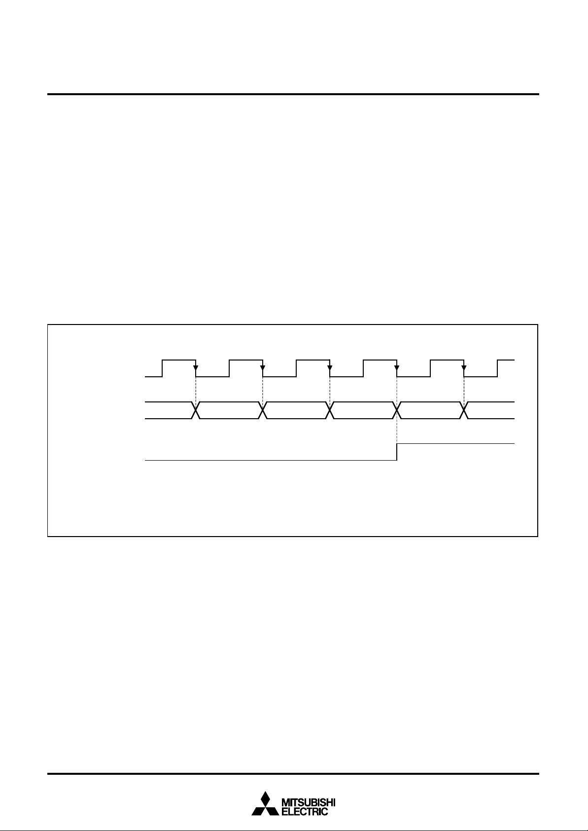
•
This symbol represents a parasitic diode on the port.
➀ Set the bit 3 of register I1 to “1” for the INT pin to be in the input
enabled state.
➁ Select the valid waveform with the bits 1 and 2 of register I1.
➂ Clear the EXF0 flag to “0” with the SNZ0 instruction.
➃ Set the NOP instruction for the case when a skip is performed
with the SNZ0 instruction.
➄ Set both the external 0 interrupt enable bit (V10) and the INTE
flag to “1.”
The external 0 interrupt is now enabled. Now when a valid waveform is input to the INT pin, the EXF0 flag is set to “1” and the
external 0 interrupt occurs.
21
Page 22
(2) External interrupt control registers
• Interrupt control register I1
Register I1 controls the valid waveform for the external 0 interrupt. Set the contents of this register through register A with the
TI1A instruction. The TAI1 instruction can be used to transfer the
contents of register I1 to register A.
Table 8 External interrupt control register
Interrupt control register I1 R/Wat RAM back-up : state retainedat reset : 00002
I13
I12
I11
I10
Notes 1: “R” represents read enabled, and “W” represents write enabled.
INT pin input control bit (Note 2)
Interrupt valid waveform for INT pin/
return level selection bit (Note 2)
INT pin edge detection circuit control bit
INT pin
timer 1 control enable bit
2: When the contents of I1
struction when the bit 0 (V1
performed with the SNZ0 instruction.
2 and I13 are changed, the external interrupt request flag EXF0 may be set. Accordingly, clear EXF0 flag with the SNZ0 in-
0) of register V1 to “0”. In this time, set the NOP instruction after the SNZ0 instruction, for the case when a skip is
0
1
0
1
0
1
0
1
MITSUBISHI MICROCOMPUTERS
4501 Group
SINGLE-CHIP 4-BIT CMOS MICROCOMPUTER
INT pin input disabled
INT pin input enabled
Falling waveform (“L” level of INT pin is recognized with the SNZI0
instruction)/“L” level
Rising waveform (“H” level of INT pin is recognized with the SNZI0
instruction)/“H” level
One-sided edge detected
Both edges detected
Disabled
Enabled
22
Page 23

MITSUBISHI MICROCOMPUTERS
4501 Group
SINGLE-CHIP 4-BIT CMOS MICROCOMPUTER
(3) Notes on interrupts
➀ Note [1] on bit 3 of register I1
When the input of the INT pin is controlled with the bit 3 of register I1 in software, be careful about the following notes.
• Depending on the input state of the P1
terrupt request flag (EXF0) may be set when the bit 3 of register
I1 is changed. In order to avoid the occurrence of an unexpected
interrupt, clear the bit 0 of register V1 to “0” (refer to Figure 18➀)
and then, change the bit 3 of register I1.
In addition, execute the SNZ0 instruction to clear the EXF0 flag
after executing at least one instruction (refer to Figure 18➁).
Also, set the NOP instruction for the case when a skip is performed with the SNZ0 instruction (refer to Figure 18➂).
•••
LA 4 ; (✕✕✕0
TV1A ; The SNZ0 instruction is valid...........➀
LA 8 ; (1✕✕✕2)
TI1A ; Control of INT pin input is changed
NOP ........................................................... ➁
SNZ0 ; The SNZ0 instruction is executed
(EXF0 flag cleared)
NOP ........................................................... ➂
2)
•••
✕ : these bits are not used here.
Fig. 18 External 0 interrupt program example-1
3/INT pin, the external 0 in-
➂ Note [3] on bit 2 of register I1
When the interrupt valid waveform of the P13/INT pin is changed
with the bit 2 of register I1 in software, be careful about the following notes.
• Depending on the input state of the P13/INT pin, the external 0 in-
terrupt request flag (EXF0) may be set when the bit 2 of register
I1 is changed. In order to avoid the occurrence of an unexpected
interrupt, clear the bit 0 of register V1 to “0” (refer to Figure 20➀)
and then, change the bit 2 of register I1 is changed.
In addition, execute the SNZ0 instruction to clear the EXF0 flag
after executing at least one instruction (refer to Figure 20➁).
Also, set the NOP instruction for the case when a skip is performed with the SNZ0 instruction (refer to Figure 20➂).
•••
LA 4 ; (✕✕✕02)
TV1A ; The SNZ0 instruction is valid...........➀
LA 12
TI1A ; Interrupt valid waveform is changed
NOP ........................................................... ➁
SNZ0 ; The SNZ0 instruction is executed
(EXF0 flag cleared)
NOP ........................................................... ➂
•••
✕ : these bits are not used here.
Fig. 20 External 0 interrupt program example-3
➁ Note [2] on bit 3 of register I1
When the bit 3 of register I1 is cleared, the RAM back-up mode is
selected and the input of INT pin is disabled, be careful about the
following notes.
• When the key-on wakeup function of port P13 is not used (regis-
ter K13 = “0”), clear bits 2 and 3 of register I1 before system
enters to the RAM back-up mode. (refer to Figure 19➀).
•••
LA 0 ; (00✕✕2)
TI1A ; Input of INT disabled........................➀
DI
EPOF
POF ; RAM back-up
•••
✕ : these bits are not used here.
Fig. 19 External 0 interrupt program example-2
23
Page 24
MITSUBISHI MICROCOMPUTERS
t
t
4501 Group
SINGLE-CHIP 4-BIT CMOS MICROCOMPUTER
TIMERS
The 4501 Group has the following timers.
• Programmable timer
The programmable timer has a reload register and enables the
frequency dividing ratio to be set. It is decremented from a setting value n. When it underflows (count to n + 1), a timer interrupt
request flag is set to “1,” new data is loaded from the reload register, and count continues (auto-reload function).
F F
1 6
n : C o u n t e r i n i t i a l v a l u e
Count starts
n
r
T
h e c o n t e n t s o f c o u n t e
00
16
1st underflow 2nd underflow
n + 1 c o u n
• Fixed dividing frequency timer
The fixed dividing frequency timer has the fixed frequency dividing ratio (n). An interrupt request flag is set to “1” after every n
count of a count pulse.
Reload Reload
n + 1 c o u n
T i m e
T i m e r i n t e r r u p t
r e q u e s t f l a g
Fig. 21 Auto-reload function
The 4501 Group timer consists of the following circuits.
• Prescaler : frequency divider
• Timer 1 : 8-bit programmable timer
• Timer 2 : 8-bit programmable timer
(Timers 1 and 2 have the interrupt function, respectively)
• 16-bit timer
Table 9 Function related timers
Circuit
Prescaler
Timer 1
Timer 2
16-bit timer
“1”
“0”
Structure
Frequency divider
8-bit programmable
binary down counter
(link to INT input)
8-bit programmable
binary down counter
16-bit fixed dividing
frequency binary down
counter
Count source
• Instruction clock
• Prescaler output (ORCLK)
• Timer 1 underflow
• Prescaler output (ORCLK)
• CNTR input
• System clock
• Instruction clock
An interrupt occurs or
a skip instruction is executed.
Prescaler and timers 1 and 2 can be controlled with the timer control registers W1, W2 and W6. The 16-bit timer is a free counter
which is not controlled with the control register.
Each function is described below.
Frequency
dividing ratio
4, 16
1 to 256
1 to 256
65536
Use of output signal
• Timer 1 and 2 count sources
• Timer 2 count source
• CNTR output
• Timer 1 interrupt
• CNTR output
• Timer 2 interrupt
• Watchdog timer
(The 16th bit is counted twice)
Control
register
W1
W1
W2
W2
24
Page 25
MITSUBISHI MICROCOMPUTERS
g
4501 Group
SINGLE-CHIP 4-BIT CMOS MICROCOMPUTER
X
I N
C l o c k
g e n e r a t i o n
c i r c u i t
D i v i s i o n c i r c u i t
d i v i d e d b y 8
d i v i d e d b y 4
d i v i d e d b y 2
I1
S y s t e m c l o c k
MR3, MR
2
1 1
10
0 1
0 0
P 13/ I N T
3
T i m e r 1 u n d e r f l o w s i g n a l
Internal clock
generating circuit
(divided by 3)
( N o t e 2 )
W 1
Rising
0
1
I1
Falling
1
Instruction clock
2
One-sided edge
0
detection circuit
1
B o t h e d g e s
d e t e c t i o n c i r c u i t
I 1
0
W 2
2
(TAB1)
P r e s c a l e r
W 1
3
0
1
ORCLK
1 / 4
1 / 1 6
I1
1
( N o t e 1 )
0
QRS
1
T i m e r 1 ( 8 )
Reload register R1 (8)
T1AB T1AB
(TR1AB)
Register B
R e g i s t e r A
W 1
0
1
(TAB1)
2
W 1
0
1
0
T i m e r 1
T 1 F
i n t e r r u p t
I n s t r u c t i o n c l o c k
W 21, W 2
0 0
01
10
1 1
P 12/ C N T R
1 6 - b i t t i m e r ( W D T )
116
WRST instruction
(Note 3)
Reset signal
D W D T i n s t r u c t i o n
+
W R S T i n s t r u c t i o n
( N o t e 4 )
W6
Timer 1 underflow signal
0
( N o t e 2 )
W2
3
0
1
Timer 2 (8)
T2F
Timer 2
interrupt
Reload register R2 (8)
(TAB2)
0
0
1
R
P1
W D F 1
W E F
2
output
QS
QRS
W6
Reset si
Register B
1
0
1
D
W D F 2
T
R
nal
(T2AB)
Register A
Q
1 / 2
1 / 2
W a t c h d o g
r e s e t s i g n a l
(TAB2)
Timer 2 underflow signal
D a t a i s s e t a u t o m a t i c a l l y f r o m e a c h r e l o a d
r e g i s t e r w h e n t i m e r 1 o r 2 u n d e r f l o w s
( a u t o - r e l o a d f u n c t i o n )
Notes 1: Timer 1 count start synchronous circuit is set
by the valid edge of P1
bits 1 (I1
1
2: Count source is stopped by clearing to “0.”
3: When the WRST instruction is executed at
4: When the DWDT and WRST instructions are
) and 2 (I12) of register I1.
WDF1 flag = “1,” WDF1 flag is cleared to “0”
and the next instruction is skipped.
When the WRST instruction is executed at
WDF1 flag = “0,” skip is not executed.
executed continuously, WEF flag is cleared to
“0” and reset by watchdog timer is not executed.
3
/INT pin selected by
Fig. 22 Timers structure
25
Page 26
Table 10 Timer control registers
MITSUBISHI MICROCOMPUTERS
4501 Group
SINGLE-CHIP 4-BIT CMOS MICROCOMPUTER
Timer control register W1 R/Wat RAM back-up : 00002
W13
W12
W11
W10
W23
W22
W21
W20
W63
W62
W61
W60
Notes 1: “R” represents read enabled, and “W” represents write enabled.
Prescaler control bit
Prescaler dividing ratio selection bit
Timer 1 control bit
Timer 1 count start synchronous circuit
control bit
Timer control register W2 R/Wat RAM back-up : state retained
Timer 2 control bit
Timer 1 count auto-stop circuit selection
bit (Note 2)
Timer 2 count source selection bits
Timer control register W6
Not used
Not used
CNTR output selection bit
P12/CNTR function selection bit
2: This function is valid only when the timer 1 count start synchronization circuit is selected.
3: CNTR input is valid only when CNTR input is selected as the timer 2 count source.
0
1
0
1
0
1
0
1
at reset : 00002
0
1
0
1
W21
W20
0
0
0
1
1
0
1
1
at reset : 00002
0
1
0
1
0
1
0
1
at reset : 00002
at reset : 00002
Stop (state initialized)
Operating
Instruction clock divided by 4
Instruction clock divided by 16
Stop (state retained)
Operating
Count start synchronous circuit not selected
Count start synchronous circuit selected
Stop (state retained)
Operating
Count auto-stop circuit not selected
Count auto-stop circuit selected
Timer 1 underflow signal
Prescaler output (ORCLK)
CNTR input
System clock
This bit has no function, but read/write is enabled.
This bit has no function, but read/write is enabled.
Timer 1 underflow signal divided by 2 output
Timer 2 underflow signal divided by 2 output
P12(I/O)/CNTR input (Note 3)
P12 (input)/CNTR input/output (Note 3)
Count source
at RAM back-up : state retained
R/Wat RAM back-up : 00002
R/W
(1) Timer control registers
• Timer control register W1
Register W1 controls the count operation of timer 1, the selection
of count start synchronous circuit, and the frequency dividing ratio and count operation of prescaler. Set the contents of this
register through register A with the TW1A instruction. The TAW1
instruction can be used to transfer the contents of register W1 to
register A.
• Timer control register W2
Register W2 controls the selection of timer 1 count auto-stop circuit, and the count operation and count source of timer 2. Set the
contents of this register through register A with the TW2A instruction. The TAW2 instruction can be used to transfer the contents
of register W2 to register A.
• Timer control register W6
Register W6 controls the P12/CNTR pin function and the selection of CNTR output. Set the contents of this register through
register A with the TW6A instruction. The TAW6 instruction can
be used to transfer the contents of register W6 to register A..
26
(2) Prescaler
Prescaler is a frequency divider. Its frequency dividing ratio can be
selected. The count source of prescaler is the instruction clock.
Use the bit 2 of register W1 to select the prescaler dividing ratio
and the bit 3 to start and stop its operation. Prescaler is initialized,
and the output signal (ORCLK) stops when the bit 3 of register W1
is cleared to “0.”
Page 27

MITSUBISHI MICROCOMPUTERS
4501 Group
SINGLE-CHIP 4-BIT CMOS MICROCOMPUTER
(3) Timer 1 (interrupt function)
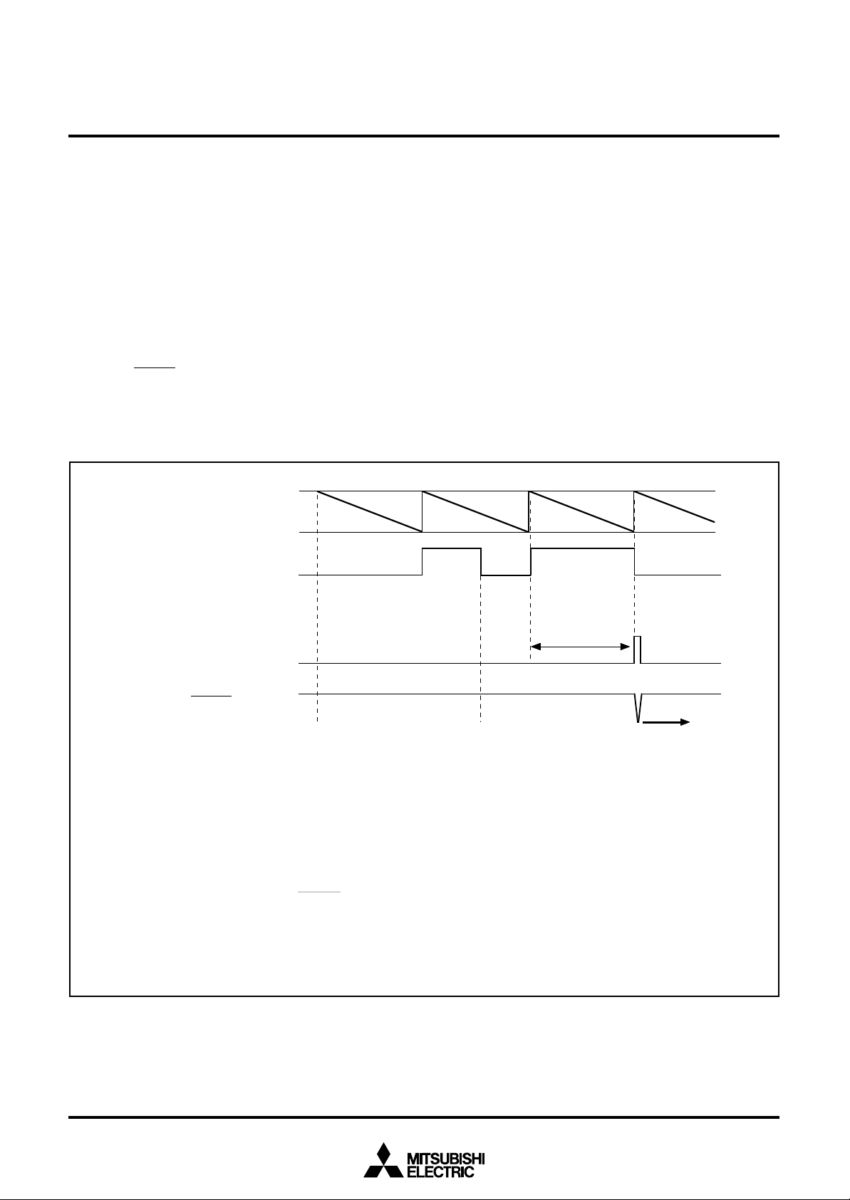
Timer 1 is an 8-bit binary down counter with the timer 1 reload register (R1). Data can be set simultaneously in timer 1 and the reload
register (R1) with the T1AB instruction. Stop counting and then execute the T1AB instruction to set data to timer 1. Data can be
written to reload register (R1) with the TR1AB instruction.
When writing data to reload register R1 with the TR1AB instruction,
the downcount after the underflow is started from the setting value
of reload register R1.
Timer 1 starts counting after the following process;
➀ set data in timer 1, and
➁ set the bit 1 of register W1 to “1.”
However, INT pin input can be used as the start trigger for timer 1
count operation by setting the bit 0 of register W1 to “1.”
Also, in this time, the auto-stop function by timer 1 underflow can
be performed by setting the bit 2 of register W2 to “1.”
When a value set is n, timer 1 divides the count source signal by n
+ 1 (n = 0 to 255).
Once count is started, when timer 1 underflows (the next count
pulse is input after the contents of timer 1 becomes “0”), the timer
1 interrupt request flag (T1F) is set to “1,” new data is loaded from
reload register R1, and count continues (auto-reload function).
Data can be read from timer 1 with the TAB1 instruction. When
reading the data, stop the counter and then execute the TAB1 instruction.
(4) Timer 2 (interrupt function)
Timer 2 is an 8-bit binary down counter with the timer 2 reload register (R2). Data can be set simultaneously in timer 2 and the reload
register (R2) with the T2AB instruction. Stop counting and then execute the T2AB instruction to set data to timer 2.
Timer 2 starts counting after the following process;
➀ set data in timer 2,
➁ select the count source with the bits 0 and 1 of register W2, and
➂ set the bit 3 of register W2 to “1.”
When a value set is n, timer 2 divides the count source signal by n
+ 1 (n = 0 to 255).
Once count is started, when timer 2 underflows (the next count
pulse is input after the contents of timer 2 becomes “0”), the timer
2 interrupt request flag (T2F) is set to “1,” new data is loaded from
reload register R2, and count continues (auto-reload function).
Data can be read from timer 2 with the TAB2 instruction. When
reading the data, stop the counter and then execute the TAB2 instruction.
(5) Timer interrupt request flags (T1F, T2F)
Each timer interrupt request flag is set to “1” when each timer
underflows. The state of these flags can be examined with the skip
instructions (SNZT1, SNZT2).
Use the interrupt control register V1 to select an interrupt or a skip
instruction.
An interrupt request flag is cleared to “0” when an interrupt occurs
or when the next instruction is skipped with a skip instruction.
(6) Count start synchronization circuit (timer 1)
Timer 1 has the count start synchronous circuit which synchronizes
the input of INT pin, and can start the timer count operation.
Timer 1 count start synchronous circuit function is selected by setting the bit 0 of register W1 to “1.” The control by INT pin input can
be performed by setting the bit 0 of register I1 to “1.”
The count start synchronous circuit is set by level change (“H”→“L”
or “L”→“H”) of INT pin input. This valid waveform is selected by bits
1 (I11) and 2 (I12) of register I1 as follows;
• I11 = “0”: Synchronized with one-sided edge (falling or rising)
• I11 = “1”: Synchronized with both edges (both falling and rising)
When register I11=“0” (synchronized with the one-sided edge), the ris-
ing or falling waveform can be selected by the bit 2 of register I1;
• I12 = “0”: Falling waveform
• I12 = “1”: Rising waveform
When timer 1 count start synchronous circuit is used, the count
start synchronous circuit is set, the count source is input to each
timer by inputting valid waveform to INT pin. Once set, the count
start synchronous circuit is cleared by clearing the bit I10 to “0” or
reset.
However, when the count auto-stop circuit is selected (register W22
= “1”), the count start synchronous circuit is cleared (auto-stop) at
the timer 1 underflow.
(7) Count auto-stop circuit (timer 1)
Timer 1 has the count auto-stop circuit which is used to stop timer
1 automatically by the timer 1 underflow when the count start synchronous circuit is used.
The count auto-stop cicuit is valid by setting the bit 2 of register W2
to “1”. It is cleared by the timer 1 underflow and the count source to
timer 1 is stopped.
This function is valid only when the timer 1 count start synchronous
circuit is selected.
27
Page 28
MITSUBISHI MICROCOMPUTERS
4501 Group
SINGLE-CHIP 4-BIT CMOS MICROCOMPUTER
(8) Timer input/output pin (P12/CNTR pin)
CNTR pin is used to input the timer 2 count source and output the
timer 1 and timer 2 underflow signal divided by 2.
The P12/CNTR pin function can be selected by bit 0 of register W6.
The CNTR output signal can be selected by bit 1 of register W6.
When the CNTR input is selected for timer 2 count source, timer 2
counts the falling waveform of CNTR input.
CNTR input
Timer 2 count
03
16
02
16
(9) Precautions
Note the following for the use of timers.
• Prescaler
Stop the prescaler operation to change its frequency dividing ratio.
• Count source
Stop timer 1 or 2 counting to change its count source.
• Reading the count value
Stop timer 1 or 2 counting and then execute the TAB1 or TAB2
instruction to read its data.
• Writing to the timer
Stop timer 1 or 2 counting and then execute the T1AB or T2AB
instruction to write its data.
• Writing to reload register R1
When writing data to reload register R1 while timer 1 is operating, avoid a timing when timer 1 underflows.
(Note)
01
16
00
16
FF
16
FE
16
Timer 2 interrupt
request flag
(T2F)
Note: This is an example when “FF
Fig. 23 Count timing diagram at CNTR input
16
” is set to timer 2 reload register R2L.
28
Page 29
WATCHDOG TIMER
Watchdog timer provides a method to reset the system when a program run-away occurs. Watchdog timer consists of timer
WDT(16-bit binary counter), watchdog timer enable flag (WEF),
and watchdog timer flags (WDF1, WDF2).
The timer WDT downcounts the instruction clocks as the count
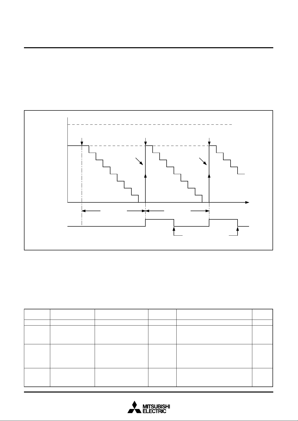
source from “FFFF16” after system is released from reset.
After the count is started, when the timer WDT underflow occurs
(after the count value of timer WDT reaches “FFFF16,” the next
count pulse is input), the WDF1 flag is set to “1.”
If the WRST instruction is never executed until the timer WDT underflow occurs (until timer WDT counts 65534), WDF2 flag is set to
“1,” and the RESET pin outputs “L” level to reset the microcomputer.
Execute the WRST instruction at each period of 65534 machine
cycle or less by software when using watchdog timer to keep the
microcomputer operating normally.
MITSUBISHI MICROCOMPUTERS
4501 Group
SINGLE-CHIP 4-BIT CMOS MICROCOMPUTER
When the WEF flag is set to “1” after system is released from reset,
the watchdog timer function is valid.
When the DWDT instruction and the WRST instruction are executed continuously, the WEF flag is cleared to “0” and the
watchdog timer function is invalid.
However, in order to set the WEF flag to “1” again once it has
cleared to “0”, execute system reset.
The WRST instruction has the skip function. When the WRST instruction is executed while the WDF1 flag is “1”, the WDF1 flag is
cleared to “0” and the next instruction is skipped.
When the WRST instruction is executed while the WDF1 flag is “0”,
the next instruction is not skipped.
The skip function of the WRST instruction can be used even when
the watchdog timer function is invalid.
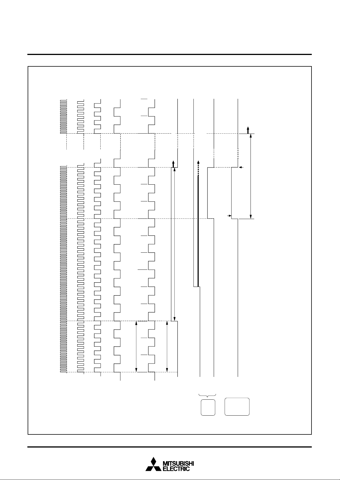
V a l u e o f 1 6 - b i t t i m e r ( W D T )
R E S E T p i n o u t p u t
➀ A f t e r s y s t e m i s r e l e a s e d f r o m r e s e t ( = a f t e r p r o g r a m i s s t a r t e d ) , t i m e r W D T s t a r t s c o u n t d o w n .
➁ W h e n t i m e r W D T u n d e r f l o w o c c u r s , W D F 1 f l a g i s s e t t o “ 1 . ”
➂ W h e n t h e W R S T i n s t r u c t i o n i s e x e c u t e d , W D F 1 f l a g i s c l e a r e d t o “ 0 , ” t h e n e x t i n s t r u c t i o n i s s k i p p e d .
➃ W h e n t i m e r W D T u n d e r f l o w o c c u r s w h i l e W D F 1 f l a g i s “ 1 , ” W D F 2 f l a g i s s e t t o “ 1 ” a n d t h e
w a t c h d o g r e s e t s i g n a l i s o u t p u t .
➄ T h e o u t p u t t r a n s i s t o r o f R E S E T p i n i s t u r n e d “ O N ” b y t h e w a t c h d o g r e s e t s i g n a l a n d s y s t e m r e s e t i s
e x e c u t e d .
F F F F
0000
W D F 1 f l a g
WDF2 flag
1 6
16
released
➁
➁
6 5 5 3 4 c o u n t
( N o t e )
➃
➂ W R S T i n s t r u c t i o n
➄ System reset➀ Reset
e x e c u t e d
( s k i p e x e c u t e d )
N o t e : T h e n u m b e r o f c o u n t i s e q u a l t o t h e n u m b e r o f c y c l e b e c a u s e t h e c o u n t s o u r c e o f w a t c h d o g t i m e r
i s t h e i n s t r u c t i o n c l o c k .
Fig. 24 Watchdog timer function
29
Page 30

When the watchdog timer is used, clear the WDF1 flag at the period of 65534 machine cycles or less with the WRST instruction.
When the watchdog timer is not used, execute the DWDT instruction and the WRST instruction continuously (refer to Figure 25).
The watchdog timer is not stopped with only the DWDT instruction.
The contents of WDF1 flag and timer WDT are initialized at the
RAM back-up mode.
When using the watchdog timer and the RAM back-up mode, initialize the WDF1 flag with the WRST instruction just before the
microcomputer enters the RAM back-up state (refer to Figure 26)
The watchdog timer function is valid after system is returned from
the RAM back-up. When not using the watchdog timer function, execute the DWDT instruction and the WRST instruction continuously
every system is returned from the RAM back-up, and stop the
watchdog timer function.
MITSUBISHI MICROCOMPUTERS
4501 Group
SINGLE-CHIP 4-BIT CMOS MICROCOMPUTER
•••
WRST ; WDF1 flag cleared
•••
DWDT ; Watchdog timer function enabled/disabled
WRST ; WEF and WDF1 flags cleared
•••
Fig. 25 Program example to start/stop watchdog timer
•••
WRST ; WDF1 flag cleared
NOP
DI ; Interrupt disabled
EPOF ; POF instruction enabled
POF
↓
Oscillation stop (RAM back-up mode)
•••
Fig. 26 Program example to enter the RAM back-up mode
when using the watchdog timer
30
Page 31

MITSUBISHI MICROCOMPUTERS
4501 Group
SINGLE-CHIP 4-BIT CMOS MICROCOMPUTER
A-D CONVERTER
The 4501 Group has a built-in A-D conversion circuit that performs
conversion by 10-bit successive comparison method. Table 11
shows the characteristics of this A-D converter. This A-D converter
can also be used as an 8-bit comparator to compare analog voltages input from the analog input pin with preset values.
Register B (4)
Register A (4)
I A P 2
( P 2
O P 2 A
( P 2
0
, P 21)
0
, P 21)
Q1
TAQ1
T Q 1 A
Q 11Q1
Q 1
3
0
2
Table 11 A-D converter characteristics
Parameter
Conversion format
Resolution
Relative accuracy
Successive comparison method
10 bits
Linearity error: ±2LSB
Characteristics
Non-linearity error: ±0.9LSB
Conversion speed
46.5 µs (High-speed mode at 4.0 MHz
oscillation frequency)
Analog input pin
2
444
4
2
TALA
8 8
TABAD
Instruction clock
1/6
TADAB
2
Q 1
3
P 20/ A
P 21/ A
I N 0
I N 1
h
A-D control circuit
Q1
1
S u c c e s s i v e c o m p a r i s o n
0
r e g i s t e r ( A D ) ( 1 0 )
3
C o m p a r a t o r
0
1
10
D A C
o p e r a t i o n
s i g n a l
2-
c h a n n el m u l t i - p l e x e d an a l o g s w i t c
DAC
10
Q 1
3
ADF
(1)
10
8
8
DA converter
V
( N o t e 1 )
S S
V
D D
C o m p a r a t o r r e g i s t e r ( 8 )
( N o t e 2 )
N o t e s 1 : T h i s s w i t c h i s t u r n e d O N o n l y w h e n A - D c o n v e r t e r i s o p e r a t i n g a n d g e n e r a t e s t h e c o m p a r i s o n v o l t a g e .
2 : W r i t i n g / r e a d i n g d a t a t o t h e c o m p a r a t o r r e g i s t e r i s p o s s i b l e o n l y i n t h e c o m p a r a t o r m o d e ( Q 1
3
= 1 ) .
T h e v a l u e o f t h e c o m p a r a t o r r e g i s t e r i s r e t a i n e d e v e n w h e n t h e m o d e i s s w i t c h e d t o t h e A - D c o n v e r s i o n
m o d e ( Q 1
3
= 0 ) b e c a u s e i t i s s e p a r a t e d f r o m t h e s u c c e s s i v e c o m p a r i s o n r e g i s t e r ( A D ) . A l s o , t h e r e s o l u t i o n
i n t h e c o m p a r a t o r m o d e i s 8 b i t s b e c a u s e t h e c o m p a r a t o r r e g i s t e r c o n s i s t s o f 8 b i t s .
01
8
Q 1
A - D
i n t e r r u p t
3
1
8
Fig. 27 A-D conversion circuit structure
31
Page 32

Table 12 A-D control registers
MITSUBISHI MICROCOMPUTERS
4501 Group
SINGLE-CHIP 4-BIT CMOS MICROCOMPUTER
A-D control register Q1
Q11
0
0
1
1
0
1
0
1
Q10
0
1
0
1
Q13
Q12
Q11
Q10
Note: “R” represents read enabled, and “W” represents write enabled.
A-D operation mode selection bit
Not used
Analog input pin selection bits
(1) Operating at A-D conversion mode
The A-D conversion mode is set by setting the bit 3 of register Q1 to “0.”
(2) Successive comparison register AD
Register AD stores the A-D conversion result of an analog input in
10-bit digital data format. The contents of the high-order 8 bits of
this register can be stored in register B and register A with the
TABAD instruction. The contents of the low-order 2 bits of this register can be stored into the high-order 2 bits of register A with the
TALA instruction. However, do not execute these instructions during A-D conversion.
When the contents of register AD is n, the logic value of the comparison voltage Vref generated from the built-in DA converter can
be obtained with the reference voltage VDD by the following formula:
Logic value of comparison voltage Vref
Vref = ✕ n
n: The value of register AD (n = 0 to 1023)
VDD
1024
at reset : 00002 at RAM back-up : state retained
A-D conversion mode
Comparator mode
This bit has no function, but read/write is enabled.
Selected pins
AIN0
AIN1
Not available
Not available
(6) Operation description
A-D conversion is started with the A-D conversion start instruction
(ADST). The internal operation during A-D conversion is as follows:
➀ When the A-D conversion starts, the register AD is cleared to
“00016.”
➁ Next, the topmost bit of the register AD is set to “1,” and the
comparison voltage Vref is compared with the analog input voltage VIN.
➂ When the comparison result is Vref < VIN, the topmost bit of the
register AD remains set to “1.” When the comparison result is
Vref > VIN, it is cleared to “0.”
The 4501 Group repeats this operation to the lowermost bit of the
register AD to convert an analog value to a digital value. A-D conversion stops after 62 machine cycles (46.5 µs when f(XIN) = 4.0
MHz in high-speed mode) from the start, and the conversion result
is stored in the register AD. An A-D interrupt activated condition is
satisfied and the ADF flag is set to “1” as soon as A-D conversion
completes (Figure 28).
R/W
(3) A-D conversion completion flag (ADF)
A-D conversion completion flag (ADF) is set to “1” when A-D conversion completes. The state of ADF flag can be examined with the
skip instruction (SNZAD). Use the interrupt control register V2 to
select the interrupt or the skip instruction.
The ADF flag is cleared to “0” when the interrupt occurs or when
the next instruction is skipped with the skip instruction.
(4) A-D conversion start instruction (ADST)
A-D conversion starts when the ADST instruction is executed. The
conversion result is automatically stored in the register AD.
(5) A-D control register Q1
Register Q1 is used to select the operation mode and one of analog input pins.
32
Page 33

Table 13 Change of successive comparison register AD during A-D conversion
At starting conversion
1st comparison
2nd comparison
3rd comparison
After 10th comparison
completes
✼1: 1st comparison result
✼3: 3rd comparison result
✼9: 9th comparison result
Change of successive comparison register AD
1
0
✼1
✼1
A-D conversion result
✼1
1
✼2
✼2
✼2: 2nd comparison result
✼8: 8th comparison result
✼A: 10th comparison result
✼3
0
0
1
-------------
-----
-------------
-------------
-----
-------------
-------------
-----
-------------
-------------
-----
-------------
0
0
0
✼8
✼9
0
0
0
0
0
0
✼A
(7) A-D conversion timing chart
Figure 28 shows the A-D conversion timing chart.
MITSUBISHI MICROCOMPUTERS
4501 Group
SINGLE-CHIP 4-BIT CMOS MICROCOMPUTER
Comparison voltage (Vref) value
VDD
2
VDD
2
VDD
2
VDD
2
±
±
±
VDD
4
VDD
4
○○○○
VDD
±
8
VDD
±
1024
A D S T i n s t r u c t i o n
A - D c o n v e r s i o n
c o m p l e t i o n f l a g ( A D F )
D A C o p e r a t i o n s i g n a l
Fig. 28 A-D conversion timing chart
(8) How to use A-D conversion
How to use A-D conversion is explained using as example in which
the analog input from P21/AIN1 pin is A-D converted, and the highorder 4 bits of the converted data are stored in address M(Z, X, Y)
= (0, 0, 0), the middle-order 4 bits in address M(Z, X, Y) = (0, 0, 1),
and the low-order 2 bits in address M(Z, X, Y) = (0, 0, 2) of RAM.
The A-D interrupt is not used in this example.
➀ Select the AIN1 pin function and A-D conversion mode with the
register Q1 (refer to Figure 29).
➁ Execute the ADST instruction and start A-D conversion.
➂ Examine the state of ADF flag with the SNZAD instruction to de-
termine the end of A-D conversion.
➃ Transfer the low-order 2 bits of converted data to the high-order
2 bits of register A (TALA instruction).
➄ Transfer the contents of register A to M (Z, X, Y) = (0, 0, 2).
➅ Transfer the high-order 8 bits of converted data to registers A
and B (TABAD instruction).
➆ Transfer the contents of register A to M (Z, X, Y) = (0, 0, 1).
➇ Transfer the contents of register B to register A, and then, store
into M(Z, X, Y) = (0, 0, 0).
6 2 m a c h i n e c y c l e s
(Bit 3) (Bit 0)
0001
Fig. 29 Setting registers
A-D control register Q1
IN1 pin selected
A
A-D conversion mode
33
Page 34

MITSUBISHI MICROCOMPUTERS
4501 Group
SINGLE-CHIP 4-BIT CMOS MICROCOMPUTER
(9) Operation at comparator mode
The A-D converter is set to comparator mode by setting bit 3 of the
register Q1 to “1.”
Below, the operation at comparator mode is described.
(10) Comparator register
In comparator mode, the built-in DA comparator is connected to the
8-bit comparator register as a register for setting comparison voltages. The contents of register B is stored in the high-order 4 bits of
the comparator register and the contents of register A is stored in
the low-order 4 bits of the comparator register with the TADAB instruction.
When changing from A-D conversion mode to comparator mode,
the result of A-D conversion (register AD) is undefined.
However, because the comparator register is separated from register AD, the value is retained even when changing from comparator
mode to A-D conversion mode. Note that the comparator register
can be written and read at only comparator mode.
If the value in the comparator register is n, the logic value of comparison voltage Vref generated by the built-in DA converter can be
determined from the following formula:
Logic value of comparison voltage Vref
VDD
Vref = ✕ n
256
n: The value of register AD (n = 0 to 255)
(11) Comparison result store flag (ADF)
In comparator mode, the ADF flag, which shows completion of A-D
conversion, stores the results of comparing the analog input voltage with the comparison voltage. When the analog input voltage is
lower than the comparison voltage, the ADF flag is set to “1.” The
state of ADF flag can be examined with the skip instruction
(SNZAD). Use the interrupt control register V2 to select the interrupt or the skip instruction.
The ADF flag is cleared to “0” when the interrupt occurs or when
the next instruction is skipped with the skip instruction.
(12) Comparator operation start instruction
(ADST instruction)
In comparator mode, executing ADST starts the comparator operating.
The comparator stops 8 machine cycles after it has started (6 µs at
f(XIN) = 4.0 MHz in high-speed mode). When the analog input voltage is lower than the comparison voltage, the ADF flag is set to “1.”
(13) Notes for the use of A-D conversion 1
Note the following when using the analog input pins also for port
P2 function:
• Selection of analog input pins
Even when P20/AIN0, P21/AIN1 are set to pins for analog input,
they continue to function as port P2 input/output. Accordingly,
when any of them are used as I/O port and others are used as
analog input pins, make sure to set the outputs of pins that are
set for analog input to “1.” Also, the port input function of the pin
functions as an analog input is undefined.
• TALA instruction
When the TALA instruction is executed, the low-order 2 bits of
register AD is transferred to the high-order 2 bits of register A, simultaneously, the low-order 2 bits of register A is “0.”
(14) Notes for the use of A-D conversion 2
Do not change the operating mode (both A-D conversion mode and
comparator mode) of A-D converter with the bit 3 of register Q1
while the A-D converter is operating.
When the operating mode of A-D converter is changed from the
comparator mode to A-D conversion mode with the bit 3 of register
Q1, note the following;
• Clear the bit 2 of register V2 to “0” to change the operating mode
of the A-D converter from the comparator mode to A-D conversion mode with the bit 3 of register Q1.
• The A-D conversion completion flag (ADF) may be set when the
operating mode of the A-D converter is changed from the comparator mode to the A-D conversion mode. Accordingly, set a
value to the bit 3 of register Q1, and execute the SNZAD instruction to clear the ADF flag.
A D S T i n s t r u c t i o n
C o m p a r i s o n r e s u l t
s t o r e f l a g ( A D F )
D A C o p e r a t i o n s i g n a l
Fig. 30 Comparator operation timing chart
34
8 m a c h i n e c y c l e s
→
Comparator operation completed.
(The value of ADF is determined)
Page 35

MITSUBISHI MICROCOMPUTERS
4501 Group
SINGLE-CHIP 4-BIT CMOS MICROCOMPUTER
(15) Definition of A-D converter accuracy
The A-D conversion accuracy is defined below (refer to Figure 31).
• Relative accuracy
➀ Zero transition voltage (V0T)
This means an analog input voltage when the actual A-D conversion output data changes from “0” to “1.”
➁ Full-scale transition voltage (VFST)
This means an analog input voltage when the actual A-D conversion output data changes from “1023” to ”1022.”
➂ Linearity error
This means a deviation from the line between V0T and VFST of
a converted value between V0T and VFST.
➃ Differential non-linearity error
This means a deviation from the input potential difference required to change a converter value between V0T and VFST by 1
LSB at the relative accuracy.
• Absolute accuracy
This means a deviation from the ideal characteristics between 0
to VDD of actual A-D conversion characteristics.
Output data
1023
Full-scale transition voltage (V
Vn: Analog input voltage when the output data changes from “n” to
“n+1” (n = 0 to 1022)
• 1LSB at relative accuracy → (V)
• 1LSB at absolute accuracy → (V)
FST
)
VFST–V0T
1022
VDD
1024
1022
Differential non-linearity error =
Linearity error =
n + 1
n
c
[ L S B ]
a
Actual A-D conversion
characteristics
a : 1 L S B b y r e l a t i v e a c c u r a c y
n + 1
– V
b : V
n
c : D i f f e r e n c e b e t w e e n i d e a l Vn
a n d a c t u a l V
1
0
n
V
1
V
0
Zero transition voltage (V0T)
Fig. 31 Definition of A-D conversion accuracy
b–a
[LSB]
a
b
a
c
I d e a l l i n e o f A - D c o n v e r s i o n
0
– V
b e t w e e n V
1 0 2 2
V
n
V
n + 1
V
1022
A n a l o g v o l t a g e
V
DD
35
Page 36

RESET FUNCTION
System reset is performed by applying “L” level to RESET pin for
1 machine cycle or more when the following condition is satisfied;
the value of supply voltage is the minimum value or more of the
recommended operating conditions.
Then when “H” level is applied to RESET pin, software starts from
address 0 in page 0.
f ( X
I N
)
MITSUBISHI MICROCOMPUTERS
4501 Group
SINGLE-CHIP 4-BIT CMOS MICROCOMPUTER
R E S E T
Fig. 32 Reset release timing
1 m a c h i n e c y c l e o r m o r e
0.85V
DD
RESET
0 . 3 V
D D
(Note)
R e s e t i n p u t
=
R i n g o s c i l l a t o r ( i n t e r n a l o s c i l l a t o r )
i s c o u n t e d 5 3 5 9 t i m e s .
Ring oscillator (internal oscillator)
Program starts
(address 0 in page 0)
is counted 5359 times.
P r o g r a m s t a r t s
( a d d r e s s 0 i n p a g e 0 )
Note: Keep the value of supply voltage to the minimum value
or more of the recommended operating conditions.
Fig. 33 RESET pin input waveform and reset operation
36
Page 37

MITSUBISHI MICROCOMPUTERS
4501 Group
SINGLE-CHIP 4-BIT CMOS MICROCOMPUTER
(1) Power-on reset
Reset can be automatically performed at power on (power-on reset) by the built-in power-on reset circuit. When the built-in
power-on reset circuit is used, the time for the supply voltage to
rise from 0 V to 2.0 V must be set to 100 µs or less. If the rising
P u l l - u p t r a n s i s t o r
( N o t e 1 )
( N o t e 2 )
R E S E T p i n
( N o t e 1 )
I n t e r n a l r e s e t s i g n a l
P o w e r - o n r e s e t c i r c u i t
V o l g a t e d r o p d e t e c t i o n c i r c u i t
W a t c h d o g r e s e t s i g n a l
WEF
N o t e s 1 :
o r l e s s
2 : A p p l i e d p o t e n t i a l t o R E S E T p i n m u s t b e VD
3 : K e e p t h e v a l u e o f s u p p l y v o l t a g e t o t h e m i n i m u m v a l u e
o r m o r e o f t h e r e c o m m e n d e d o p e r a t i n g c o n d i t i o n s .
time exceeds 100 µs, connect a capacitor between the RESET pin
and VSS at the shortest distance, and input “L” level to RESET pin
until the value of supply voltage reaches the minimum operating
voltage.
1 0 0 µs o r l e s s
I n t e r n a l r e s e t s i g n a l
R e s e t
s t a t e
P o w e r - o n
T h i s s y m b o l r e p r e s e n t s a p a r a s i t i c d i o d e .
Reset released
V
D D
( N o t e 3 )
Power-on reset circuit output
D
.
Fig. 34 Power-on reset circuit example
Table 14 Port state at reset
Name
D0, D1
D2/C, D3/K
P00, P01, P02, P03
P10, P11, P12/CNTR, P13/INT
P20/AIN0, P21/AIN1
Notes 1: Output latch is set to “1.”
2: Pull-up transistor is turned OFF.
D0, D1
D2, D3
P00–P03
P10–P13
P20, P21
Function
State
High-impedance (Note 1)
High-impedance (Notes 1, 2)
High-impedance (Notes 1, 2)
High-impedance (Notes 1, 2)
High-impedance (Notes 1, 2)
37
Page 38

(2) Internal state at reset
Figure 35 shows internal state at reset (they are the same after system is released from reset). The contents of timers, registers, flags
and RAM except shown in Figure 35 are undefined, so set the initial value to them.
MITSUBISHI MICROCOMPUTERS
4501 Group
SINGLE-CHIP 4-BIT CMOS MICROCOMPUTER
• Program counter (PC) ..........................................................................................................
Address 0 in page 0 is set to program counter.
• Interrupt enable flag (INTE)..................................................................................................
• Power down flag (P) .............................................................................................................
• External 0 interrupt request flag (EXF0) ..............................................................................
• Interrupt control register V1..................................................................................................
• Interrupt control register V2..................................................................................................
• Interrupt control register I1 ...................................................................................................
• Timer 1 interrupt request flag (T1F) .....................................................................................
• Timer 2 interrupt request flag (T2F) .....................................................................................
• Watchdog timer flags (WDF1, WDF2)..................................................................................
• Watchdog timer enable flag (WEF) ......................................................................................
• Timer control r e g i s t e r W 1 .....................................................................................................
• Timer control r e g i s t e r W 2 .....................................................................................................
• Timer control r e g i s t e r W 6 .....................................................................................................
• Clock control register MR .....................................................................................................
• Key-on wakeup control register K0 ......................................................................................
• Key-on wakeup control register K1 ......................................................................................
• Key-on wakeup control register K2 ......................................................................................
• Pull-up control register PU0 .................................................................................................
• Pull-up control register PU1 .................................................................................................
• Pull-up control register PU2 .................................................................................................
• A-D conversion completion flag (ADF).................................................................................
• A-D control register Q1.........................................................................................................
• Carry flag (CY)......................................................................................................................
• Register A .............................................................................................................................
• Register B .............................................................................................................................
• Register D .............................................................................................................................
• Register E .............................................................................................................................
• Register X .............................................................................................................................
• Register Y .............................................................................................................................
• Register Z .............................................................................................................................
• Stack pointer (SP) ................................................................................................................
• Oscillation clock .......................................................................... Ring oscillator (operating)
• Ceramic resonator circuit ..................................................................................... Operating
• RC oscillation circuit ......................................................................................................Stop
00000000000000
0 0 0 0 (Interrupt disabled)
0 0 0 0 (Interrupt disabled)
0000
0 0 0 0 (Prescaler and timer 1 stopped)
0 0 0 0 (Timer 2 stopped)
0000
1100
0000
0000
0000
0000
0000
0000
0000
0000
0000
✕✕✕
✕✕✕✕✕✕
✕✕
0000
0000
✕✕
111
0 (Interrupt disabled)
0
0
0
0
0
1
0
0
Fig. 35 Internal state at reset
38
“✕” represents undefined.
Page 39

VOLTAGE DROP DETECTION CIRCUIT
–
The built-in voltage drop detection circuit is designed to detect a
drop in voltage and to reset the microcomputer if the supply voltage
drops below a set value.
MITSUBISHI MICROCOMPUTERS
4501 Group
SINGLE-CHIP 4-BIT CMOS MICROCOMPUTER
V
D D
V R S T
(Note 2)
+
Voltage drop detection circuit
Notes 1: In the RAM back-up mode by the POF2 instruction,
the voltage drop detection circuit stops.
2: When the V
the voltage drop detection circuit reset signal is output.
Fig. 36 Voltage drop detection reset circuit
V
DD
VRST
(detection voltage)
Q S
(Note 1)
V o l t a g e d r o p d e t e c t i o n c i r c u i t
r e s e t s i g n a l
DD
(supply voltage) is VRST (detection voltage) or less,
EPOF instruction +POF2 instruction
(continuousu execution)
R
Reset signal
R e t u r n i n p u t
N o t e 3
V o l t a g e d r o p d e t e c t i o n
c i r c u i t r e s e t s i g n a l
R E S E T p i n
N o t e s 1 : A f t e r s y s t e m i s r e l e a s e d f r o m r e s e t , t h e r i n g o s c i l l a t o r ( i n t e r n a l o s c i l l a t o r )
i s s e l e c t e d a s t h e o p e r a t i o n c l o c k o f t h e m i c r o c o m p u t e r .
2 : R e f e r t o t h e v o l t a g e d r o p d e t e c t i o n c i r c u i t i n t h e e l e c t r i c a l c h a r a c t e r i s t i c s
f o r t h e r a t i n g v a l u e o f V R S T ( d e t e c t i o n v o l t a g e ) .
3 : T h e V R S T ( d e t e c t i o n v o l t a g e ) d o e s n o t i n c l u d e h y s t e r e s i s .
Fig. 37 Voltage drop detection circuit operation waveform
The microcomputer starts
operation after the ring
oscillator (internal oscillator) is
counted 5359 times.
39
Page 40

MITSUBISHI MICROCOMPUTERS
4501 Group
SINGLE-CHIP 4-BIT CMOS MICROCOMPUTER
RAM BACK-UP MODE
The 4501 Group has the RAM back-up mode.
When the POF or POF2 instruction is executed continuously after
the EPOF instruction, system enters the RAM back-up state.
The POF or POF2 instruction is equal to the NOP instruction when
the EPOF instruction is not executed before the POF or POF2 instruction.
As oscillation stops retaining RAM, the function of reset circuit and
states at RAM back-up mode, current dissipation can be reduced
without losing the contents of RAM.
In the RAM back-up mode by the POF instruction, system enters
the RAM back-up mode and the voltage drop detection cicuit keeps
operating.
In the RAM back-up mode by the POF2 instruction, all internal
periperal functions stop.
Table 15 shows the function and states retained at RAM back-up.
Figure 38 shows the state transition.
(1) Identification of the start condition
Warm start (return from the RAM back-up state) or cold start (return from the normal reset state) can be identified by examining the
state of the power down flag (P) with the SNZP instruction.
(2) Warm start condition
When the external wakeup signal is input after the system enters
the RAM back-up state by executing the EPOF instruction and
POF or POF2 instruction continuously, the CPU starts executing
the program from address 0 in page 0. In this case, the P flag is
“1.”
(3) Cold start condition
The CPU starts executing the program from address 0 in page 0
when;
• reset pulse is input to RESET pin, or
• reset by watchdog timer is performed, or
• voltage drop detection circuit is detected by the voltage drop
In this case, the P flag is “0.”
Table 15 Functions and states retained at RAM back-up
Function
Program counter (PC), registers A, B,
carry flag (CY), stack pointer (SP) (Note 2)
Contents of RAM
Port level
Selected oscillation circuit
Timer control register W1
Timer control registers W2, W6
Clock control register MR
Interrupt control registers V1, V2
Interrupt control register I1
Timer 1 function
Timer 2 function
A-D conversion function
Voltage drop detection circuit
A-D control register Q1
Pull-up control registers PU0 to PU2
Key-on wakeup control registers K0 to K2
External 0 interrupt request flag (EXF0)
Timer 1 interrupt request flag (T1F)
Timer 2 interrupt request flag (T2F)
Watchdog timer flags (WDF1)
Watchdog timer enable flag (WEF)
16-bit timer (WDT)
A-D conversion completion flag (ADF)
Interrupt enable flag (INTE)
Notes 1:“O” represents that the function can be retained, and “✕” repre-
sents that the function is initialized.
Registers and flags other than the above are undefined at RAM
back-up, and set an initial value after returning.
2: The stack pointer (SP) points the level of the stack register and is
initialized to “7” at RAM back-up.
3: The state of the timer is undefined.
4: Initialize the watchdog timer with the WRST instruction, and then
execute the POF or POF2 instruction.
5: This function is operating in the RAM back-up mode. When the
voltage drop is detected, system reset occurs.
RAM back-up
POF
✕
O
O
O
✕
O
✕
✕
O
✕
(Note 3)
✕
O (Note 5)
O
O
O
✕
✕
(Note 3)
✕ (Note 4)
✕
✕ (Note 4)
✕
✕
POF2
✕
O
O
O
✕
O
✕
✕
O
✕
(Note 3)
✕
✕
O
O
O
✕
✕
(Note 3)
✕ (Note 4)
✕
✕ (Note 4)
✕
✕
40
Page 41

MITSUBISHI MICROCOMPUTERS
4501 Group
SINGLE-CHIP 4-BIT CMOS MICROCOMPUTER
(4) Return signal
An external wakeup signal is used to return from the RAM back-up
mode because the oscillation is stopped. Table 16 shows the return
condition for each return source.
(5) Control registers
• Key-on wakeup control register K0
Register K0 controls the port P0 key-on wakeup function. Set the
contents of this register through register A with the TK0A instruction. In addition, the TAK0 instruction can be used to transfer the
contents of register K0 to register A.
• Key-on wakeup control register K1
Register K1 controls the port P1 key-on wakeup function. Set the
contents of this register through register A with the TK1A instruction. In addition, the TAK1 instruction can be used to transfer the
contents of register K0 to register A.
• Key-on wakeup control register K2
Register K2 controls the ports P2, D2/C and D3/K key-on wakeup
function. Set the contents of this register through register A with
the TK2A instruction. In addition, the TAK2 instruction can be
used to transfer the contents of register K2 to register A.
Table 16 Return source and return condition
Return source
Port P0
Port P1 (Note)
Port P2
Ports D2/C, D3/K
Port P13/INT
(Note)
External wakeup signal
Note: When the bit 3 (K13) of register K1 is “0”, the key-on wakeup of the INT pin is valid (“H” or “L” level).
It is “1”, the key-on wakeup of port P1
Return by an external “L” level input.
Return by an external “H” level or
“L” level input. The return level
can be selected with the bit 2
(I12) of register I1.
When the return level is input, the
EXF0 flag is not set.
Return condition
The key-on wakeup function can be selected by one port unit. Set the port
using the key-on wakeup function to “H” level before going into the RAM
back-up state.
Select the return level (“L” level or “H” level) with the bit 2 of register I1 according to the external state before going into the RAM back-up state.
3 is valid (“L” level).
• Pull-up control register PU0
Register PU0 controls the ON/OFF of the port P0 pull-up transistor. Set the contents of this register through register A with the
TPU0A instruction.
• Pull-up control register PU1
Register PU1 controls the ON/OFF of the port P1 pull-up transistor. Set the contents of this register through register A with the
TPU1A instruction.
• Pull-up control register PU2
Register PU2 controls the ON/OFF of the ports P2, D
K pull-up transistor. Set the contents of this register through register A with the TPU2A instruction.
• Interrupt control register I1
Register I1 controls the valid waveform of the external 0 interrupt, the input control of INT pin and the return input level. Set
the contents of this register through register A with the TI1A instruction. In addition, the TAI1 instruction can be used to transfer
the contents of register I1 to register A.
2/C and D3/
Remarks
41
Page 42

MITSUBISHI MICROCOMPUTERS
Q
P
t
4501 Group
SINGLE-CHIP 4-BIT CMOS MICROCOMPUTER
D
R A M b a c k - u p
( V o l t a g e d r o p d e t e c t i o n
c i r c u i t i s o p e r a t i n g . )
Operation source clock: stop
P O F i n s t r u c t i o n e x e c u t i o n
K e y - o n w a k e u p
( S t a b i l i z i n g t i m e b )
P O F i n s t r u c t i o n e x e c u t i o n
V o l t a g e d r o p
d e t e c t e d
R e s e t
Key-on wakeup
(Stabilizing time a )
POF instruction execution
Key-on wakeup
( S t a b i l i z i n g t i m e c )
( S t a b i l i z i n g
t i m e a )
B
Operating
Operation source clock:
ceramic resonator
Ring oscillator: stop
RC oscillation circuit: stop
CMCK instruction
execution (Note 3)
A
O p e r a t i n g
O p e r a t i o n s o u r c e c l o c k :
r i n g o s c i l l a t o r c l o c k
C e r a m i c r e s o n a t o r :
o p e r a t i n g (N o t e 2)
R C o s c i l l a t i o n c i r c u i t : s t o p
CRCK instruction
execution (Note 3)
C
Operating
Operation source clock:
RC oscillation
Ring oscillator: stop
Ceramic resonator: stop
P O F 2 i n s t r u c t i o n e x e c u t i o n
Key-on wakeup
( S t a b i l i z i n g t i m e b )
POF2 instruction execution
Key-on wakeup
(Stabilizing time a )
POF2 instruction execution
Key-on wakeup
( S t a b i l i z i n g t i m e c )
E
R A M b a c k - u p
( A l l f u n c t i o n s o f
m i c r o c o m p u t e r s t o p )
Operation source clock: stop
Stabilizing time a : Microcomputer starts its operation after counting the ring oscillator clock 5359 times by hardware.
Stabilizing time b : Microcomputer starts its operation after counting the f(X
Stabilizing time c : Microcomputer starts its operation after counting the f(X
Notes 1: Continuous execution of the EPOF instruction and the POF or POF2 instruction is required to go into
the RAM back-up state.
2: Through the ceramic resonator is operating, the ring oscillator clock is selected as the operation source clock.
3: The oscillator clock corresponding to each instruction is selected as the operation source clock,
and the ring oscillator is stopped.
Fig. 38 State transition
Power down flag
S
R
• • • • • • •
E P O F i n s t r u c t i o n +
• • • • • •
EPOF instruction +
P O F o r
P O F 2
i n s t r u c t i o n
Reset inpu
● Set source
● Clear source Reset input
Fig. 39 Set source and clear source of the P flag
POF or
POF2
instruction
IN
) 5359 times by hardware.
IN
) 165 times by hardware.
Program start
P = “ 1 ”
Yes
?
No
Cold start
Fig. 40 Start condition identified example using the SNZP in-
struction
Warm start
42
Page 43

Table 17 Key-on wakeup control register
MITSUBISHI MICROCOMPUTERS
4501 Group
SINGLE-CHIP 4-BIT CMOS MICROCOMPUTER
Key-on wakeup control register K0
K03
K02
K01
K00
K13
K12
K11
K10
K23
K22
K21
K20
Note: “R” represents read enabled, and “W” represents write enabled.
Port P03 key-on wakeup
control bit
Port P02 key-on wakeup
control bit
Port P01 key-on wakeup
control bit
Port P00 key-on wakeup
control bit
Key-on wakeup control register K1
Port P13/INT key-on wakeup
control bit
Port P12/CNTR key-on wakeup
control bit
Port P11 key-on wakeup
control bit
Port P10 key-on wakeup
control bit
Key-on wakeup control register K2
Port D3/K key-on wakeup
control bit
Port D2/C key-on wakeup
control bit
Port P21/AIN1 key-on wakeup
control bit
Port P20/AIN0 key-on wakeup
control bit
at reset : 00002 at RAM back-up : state retained
0
Key-on wakeup not used
1
Key-on wakeup used
0
Key-on wakeup not used
1
Key-on wakeup used
0
Key-on wakeup not used
1
Key-on wakeup used
0
Key-on wakeup not used
1
Key-on wakeup used
at reset : 00002 at RAM back-up : state retained
0
P13 key-on wakeup not used/INT pin key-on wakeup used
1
P13 key-on wakeup used/INT pin key-on wakeup not used
0
Key-on wakeup not used
1
Key-on wakeup used
0
Key-on wakeup not used
1
Key-on wakeup used
0
Key-on wakeup not used
1
Key-on wakeup used
at reset : 00002 at RAM back-up : state retained
0
Key-on wakeup not used
1
Key-on wakeup used
0
Key-on wakeup not used
1
Key-on wakeup used
0
Key-on wakeup not used
1
Key-on wakeup used
0
Key-on wakeup not used
1
Key-on wakeup used
R/W
R/W
R/W
43
Page 44

Table 18 Pull-up control register and interrupt control register
MITSUBISHI MICROCOMPUTERS
4501 Group
SINGLE-CHIP 4-BIT CMOS MICROCOMPUTER
PU03
PU02
PU01
PU00
PU13
PU12
PU11
PU10
PU23
PU22
PU21
PU20
Pull-up control register PU0
Port P0
3 pull-up transistor
control bit
Port P02 pull-up transistor
control bit
Port P01 pull-up transistor
control bit
Port P00 pull-up transistor
control bit
Pull-up control register PU1 at reset : 00002 at RAM back-up : state retained
Port P13/INT pull-up transistor
control bit
Port P12/CNTR pull-up transistor
control bit
Port P11 pull-up transistor
control bit
Port P10 pull-up transistor
control bit
Pull-up control register PU2
Port D3/K pull-up transistor
control bit
Port D2/C pull-up transistor
control bit
Port P21/AIN1 pull-up transistor
control bit
Port P20/AIN0 pull-up transistor
control bit
at reset : 00002 at RAM back-up : state retained
0
Pull-up transistor OFF
1
Pull-up transistor ON
0
Pull-up transistor OFF
1
Pull-up transistor ON
0
Pull-up transistor OFF
1
Pull-up transistor ON
0
Pull-up transistor OFF
1
Pull-up transistor ON
0
Pull-up transistor OFF
1
Pull-up transistor ON
0
Pull-up transistor OFF
1
Pull-up transistor ON
0
Pull-up transistor OFF
1
Pull-up transistor ON
0
Pull-up transistor OFF
1
Pull-up transistor ON
at reset : 00002 at RAM back-up : state retained
0
Pull-up transistor OFF
1
Pull-up transistor ON
0
Pull-up transistor OFF
1
Pull-up transistor ON
0
Pull-up transistor OFF
1
Pull-up transistor ON
0
Pull-up transistor OFF
1
Pull-up transistor ON
W
W
W
Interrupt control register I1
I13
I12
I11
I10
Notes 1: “R” represents read enabled, and “W” represents write enabled.
44
INT pin input control bit (Note 2)
Interrupt valid waveform for INT pin/
return level selection bit (Note 2)
INT pin edge detection circuit control bit
INT pin
timer 1 control enable bit
2: When the contents of I1
struction when the bit 0 (V1
performed with the SNZ0 instruction.
2 and I13 are changed, the external interrupt request flag EXF0 may be set. Accordingly, clear EXF0 flag with the SNZ0 in-
0) of register V1 to “0”. In this time, set the NOP instruction after the SNZ0 instruction, for the case when a skip is
0
1
0
1
0
1
0
1
at reset : 00002
INT pin input disabled
INT pin input enabled
Falling waveform (“L” level of INT pin is recognized with the SNZI0
instruction)/“L” level
Rising waveform (“H” level of INT pin is recognized with the SNZI0
instruction)/“H” level
One-sided edge detected
Both edges detected
Disabled
Enabled
at RAM back-up : state retained
R/W
Page 45

MITSUBISHI MICROCOMPUTERS
4501 Group
SINGLE-CHIP 4-BIT CMOS MICROCOMPUTER
CLOCK CONTROL
The clock control circuit consists of the following circuits.
• Ring oscillator (internal oscillator)
• Ceramic oscillator
• RC oscillation circuit
• Multi-plexer (clock selection circuit)
• Frequency divider
• Internal clock generating circuit
R i n g o s c i l l a t o r
( i n t e r n a l o s c i l l a t o r )
( N o t e 1 )
R C o s c i l l a t i o n c i r c u i t
X
IN
X
O U T
Ceramic resonator
circuit
M u l t i p l e x e r
QS
QR
Division circuit
divided by 8
divided by 4
divided by 2
The system clock and the instruction clock are generated as the
source clock for operation by these circuits.
Figure 41 shows the structure of the clock control circuit.
The 4501 Group operates by the ring oscillator clock (f(RING))
which is the internal oscillator after system is released from reset.
Also, the ceramic resonator or the RC oscillation can be used for
the source oscillation (f(XIN)) of the 4501 Group. The CMCK instruction or CRCK instruction is executed to select the ceramic
resonator or RC oscillator, respectively.
M R
3 ,
M R
2
1 1
1 0
0 1
0 0
QS
R
S y s t e m c l o c k
Internal clock
generation circuit
(divided by 3)
C R C K i n s t r u c t i o n
Instruction clock
Counter
Wait time (Note 2)
control circuit
P r o g r a m
s t a r t s i g n a l
N o t e s 1 : S y s t e m o p e r a t e s b y t h e r i n g o s c i l l a t o r c l o c k ( f ( R I N G ) ) u n t i l t h e C M C K o r C R C K i n s t r u c t i o n
i s e x e c u t e d a f t e r s y s t e m i s r e l e a s e d f r o m r e s e t .
2 : T h e w a i t t i m e c o n t r o l c i r c u i t i s u s e d t o g e n e r a t e t h e t i m e r e q u i r e d t o s t a b i l i z e t h e f ( X
A f t e r t h e c e r t a i n o s c i l l a t i o n s t a b i l i z i n g w a i t t i m e e l a p s e s , t h e p r o g r a m s t a r t s i g n a l i s o u t p u t .
T h i s c i r c u i t o p e r a t e s w h e n s y s t e m i s r e l e a s e d f r o m r e s e t o r r e t u r n e d f r o m R A M b a c k - u p .
Fig. 41 Clock control circuit structure
QS
R
QS
R
POF or
EPOF instruction + POF2
instruction
CMCK
instruction
RESET pin
Key-on wakeup signal
I N
) o s c i l l a t i o n .
45
Page 46

MITSUBISHI MICROCOMPUTERS
4501 Group
SINGLE-CHIP 4-BIT CMOS MICROCOMPUTER
(1) Selection of source oscillation (f(XIN))
The ceramic resonator or RC oscillation can be used for the source
oscillation of the MCU.
After system is released from reset, the MCU starts operation by
the clock output from the ring oscillator which is the internal oscillator.
When the ceramic resonator is used, execute the CMCK instruction. When the RC oscillation is used, execute the CRCK
instruction. The oscillation circuit by the CMCK or CRCK instruction
can be selected only at once. The oscillation circuit corresponding
to the first executed one of these two instructions is valid. Other oscillation circuit and the ring oscillator stop.
Execute the CMCK or the CRCK instruction in the initial setting routine of program (executing it in address 0 in page 0 is
recommended). Also, when the CMCK or the CRCK instruction is
not executed in program, the MCU operates by the ring oscillator.
(2) Ring oscillator operation
When the MCU operates by the ring oscillator as the source oscillation (f(XIN)) without using the ceramic resonator or the RC
oscillator, connect XIN pin to VSS and leave XOUT pin open (Figure
43).
The clock frequency of the ring oscillator depends on the supply
voltage and the operation temperature range.
Be careful that variable frequencies when designing application
products.
(3) Ceramic resonator
When the ceramic resonator is used as the source oscillation
(f(XIN)), connect the ceramic resonator and the external circuit to
pins XIN and XOUT at the shortest distance. Then, execute the
CMCK instruction. A feedback resistor is built in between pins XIN
and XOUT (Figure 44).
(4) RC oscillation
When the RC oscillation is used as the source oscillation (f(XIN)),
connect the XIN pin to the external circuit of resistor R and the capacitor C at the shortest distance and leave XOUT pin open. Then,
execute the CRCK instruction (Figure 45).
The frequency is affected by a capacitor, a resistor and a microcomputer. So, set the constants within the range of the frequency
limits.
R e s e t
R i n g o s c i l l a t o r
o p e r a t i o n
CMCK instruction
• Ceramic resonator valid
• Ring oscillator stop
• RC oscillation stop
Fig. 42 Switch to ceramic resonance/RC oscillation
4501
XIN XO
Fig. 43 Handling of XIN and XOUT when operating ring oscillator
U
4501
Do not use the CMCK instruction
*
and CRCK instruction in program.
T
*
X
IN
IN
C
Fig. 44 Ceramic resonator external circuit
R
X
OUT
R d
C
4 5 0 1
XI
N XO U T
OUT
C R C K i n s t r u c t i o n
• R C o s c i l l a t i o n v a l i d
• R i n g o s c i l l a t o r s t o p
• C e r a m i c r e s o n a t o r s t o p
Execute the CMCK instruction in program.
Note: Externally connect a damping
resistor Rd depending on the
oscillation frequency.
(A feedback resistor is built-in.)
Use the resonator manufacturer’s recommended value
because constants such as capacitance depend on the
resonator.
E x e c u t e t h e C R C K
*
i n s t r u c t i o n i n p r o g r a m .
46
C
Fig. 45 External RC oscillation circuit
Page 47

(5) External clock
When the external signal clock is used as the source oscillation
(f(XIN)), connect the XIN pin to the clock source and leave XOUT pin
open. Then, execute the CMCK instruction (Figure 46).
Be careful that the maximum value of the oscillation frequency
when using the external clock differs from the value when using the
ceramic resonator (refer to the recommended operating condition).
Also, note that the RAM back-up mode (POF and POF2 instructions) cannot be used when using the external clock.
MITSUBISHI MICROCOMPUTERS
4501 Group
SINGLE-CHIP 4-BIT CMOS MICROCOMPUTER
E x e c u t e t h e C M C K
4501
X
I N
X
O U T
*
i n s t r u c t i o n i n p r o g r a m .
V
D D
V
SS
(6) Clock control register MR
Register MR controls system clock. Set the contents of this register
through register A with the TMRA instruction. In addition, the TAMR
instruction can be used to transfer the contents of register MR to
register A.
Table 19 Clock control register MR
Clock control register MR
MR3
System clock selection bits
MR2
MR1
MR0
Note : “R” represents read enabled, and “W” represents write enabled.
Not used
Not used
at reset : 11002 at RAM back-up : 11002
MR3
MR2
0
0
0
1
1
0
1
1
0
1
0
1
ROM ORDERING METHOD
Please submit the information described below when ordering
Mask ROM.
(1) Mask ROM Order Confirmation Form ..................................... 1
(2) Data to be written into mask ROM ...............................EPROM
(three sets containing the identical data)
(3) Mark Specification Form .......................................................... 1
E x t e r n a l o s c i l l a t i o n c i r c u i t
Fig. 46 External clock input circuit
R/W
System clock
f(XIN) (high-speed mode)
f(XIN)/2 (middle-speed mode)
f(XIN)/4 (low-speed mode)
f(XIN)/8 (default mode)
This bit has no function, but read/write is enabled.
This bit has no function, but read/write is enabled.
47
Page 48

MITSUBISHI MICROCOMPUTERS
4501 Group
SINGLE-CHIP 4-BIT CMOS MICROCOMPUTER
LIST OF PRECAUTIONS
➀Noise and latch-up prevention
Connect a capacitor on the following condition to prevent noise
and latch-up;
• connect a bypass capacitor (approx. 0.1
and VSS at the shortest distance,
• equalize its wiring in width and length, and
• use relatively thick wire.
In the One Time PROM version, CNVSS pin is also used as VPP
pin. Accordingly, when using this pin, connect this pin to VSS
through a resistor about 5 kΩ (connect this resistor to CNVSS/
VPP pin as close as possible).
➁Register initial values 1
The initial value of the following registers are undefined after system is released from reset. After system is released from reset,
set initial values.
• Register Z (2 bits)
• Register D (3 bits)
• Register E (8 bits)
➂Register initial values 2
The initial value of the following registers are undefined at RAM
back-up. After system is returned from RAM back-up, set initial
values.
• Register Z (2 bits)
• Register X (4 bits)
• Register Y (4 bits)
• Register D (3 bits)
• Register E (8 bits)
➃ Stack registers (SKS) and stack pointer (SP)
Stack registers (SKs) are eight identical registers, so that subroutines can be nested up to 8 levels. However, one of stack
registers is used respectively when using an interrupt service
routine and when executing a table reference instruction. Accordingly, be careful not to over the stack when performing these
operations together.
➄Prescaler
Stop the prescaler operation to change its frequency dividing ratio.
➅Timer count source
Stop timer 1 or 2 counting to change its count source.
µ
F) between pins VDD
10
Watchdog timer
• The watchdog timer function is valid after system is released
from reset. When not using the watchdog timer function, execute
the DWDT instruction and the WRST instruction continuously,
and clear the WEF flag to “0” to stop the watchdog timer function.
• The watchdog timer function is valid after system is returned from
the RAM back-up. When not using the watchdog timer function,
execute the DWDT instruction and the WRST instruction continuously every system is returned from the RAM back-up, and stop
the watchdog timer function.
11
Multifunction
• The input/output of D2, D3, P12 and P13 can be used even when
C, K, INT and CNTR (input) are selected.
• The input of P12 can be used even when CNTR (output) is selected.
• The input/output of P20 and P21 can be used even when AIN0 and
AIN1 are selected.
12
Program counter
Make sure that the PCH does not specify after the last page of
the built-in ROM.
13
POF and POF2 instructions
When the POF or POF2 instruction is executed continuously after the EPOF instruction, system enters the RAM back-up state.
Note that system cannot enter the RAM back-up state when executing only the POF or POF2 instruction.
Be sure to disable interrupts by executing the DI instruction before executing the EPOF instruction and the POF or POF2
instruction continuously.
14
P13/INT pin
Note [1] on bit 3 of register I1
When the input of the INT pin is controlled with the bit 3 of register I1 in software, be careful about the following notes.
• Depending on the input state of the P13/INT pin, the external 0 in-
terrupt request flag (EXF0) may be set when the bit 3 of register
I1 is changed. In order to avoid the occurrence of an unexpected
interrupt, clear the bit 0 of register V1 to “0” (refer to Figure 47➀)
and then, change the bit 3 of register I1.
In addition, execute the SNZ0 instruction to clear the EXF0 flag
after executing at least one instruction (refer to Figure 47➁).
Also, set the NOP instruction for the case when a skip is performed with the SNZ0 instruction (refer to Figure 47➂).
➆ Reading the count value
Stop timer 1 or 2 counting and then execute the TAB1 or TAB2
instruction to read its data.
➇Writing to the timer
Stop timer 1 or 2 counting and then execute the T1AB or T2AB
instruction to write its data.
➈Writing to reload register R1
When writing data to reload register R1 while timer 1 is operating, avoid a timing when timer 1 underflows.
48
•••
LA 4 ; (✕✕✕02)
TV1A ; The SNZ0 instruction is valid...........➀
LA 8 ; (1✕✕✕2)
TI1A ; Control of INT pin input is changed
NOP ........................................................... ➁
SNZ0 ; The SNZ0 instruction is executed
(EXF0 flag cleared)
NOP ........................................................... ➂
•••
✕ : these bits are not used here.
Fig. 47 External 0 interrupt program example-1
Page 49

Note [2] on bit 3 of register I1
When the bit 3 of register I1 is cleared, the RAM back-up mode is
selected and the input of INT pin is disabled, be careful about the
following notes.
• When the key-on wakeup function of port P13 is not used (regis-
ter K13 = “0”), clear bits 2 and 3 of register I1 before system
enters to the RAM back-up mode. (refer to Figure 48➀).
MITSUBISHI MICROCOMPUTERS
4501 Group
SINGLE-CHIP 4-BIT CMOS MICROCOMPUTER
15
Power-on reset
Reset can be automatically performed at power on (power-on reset) by the built-in power-on reset circuit. When the built-in
power-on reset circuit is used, the time for the supply voltage to
rise from 0 V to 2.0 V must be set to 100 µs or less. If the rising
time exceeds 100 µs, connect a capacitor between the RESET
pin and VSS at the shortest distance, and input “L” level to RESET pin until the value of supply voltage reaches the minimum
operating voltage.
•••
LA 0 ; (00✕✕2)
TI1A ; Input of INT disabled........................➀
DI
EPOF
POF ; RAM back-up
•••
✕ : these bits are not used here.
Fig. 48 External 0 interrupt program example-2
Note [3] on bit 2 of register I1
When the interrupt valid waveform of the P13/INT pin is changed
with the bit 2 of register I1 in software, be careful about the following notes.
• Depending on the input state of the P13/INT pin, the external 0 in-
terrupt request flag (EXF0) may be set when the bit 2 of register
I1 is changed. In order to avoid the occurrence of an unexpected
interrupt, clear the bit 0 of register V1 to “0” (refer to Figure 49➀)
and then, change the bit 2 of register I1.
In addition, execute the SNZ0 instruction to clear the EXF0 flag
after executing at least one instruction (refer to Figure 49➁).
Also, set the NOP instruction for the case when a skip is performed with the SNZ0 instruction (refer to Figure 49➂).
16
Clock control
Execute the CMCK or the CRCK instruction in the initial setting
routine of program (executing it in addres 0 in page 0 is recommended).
The oscillation circuit by the CMCK or CRCK instruction can be
selected only at once. The oscillation circuit corresponding to the
first executed one of these two instruction is valid. Other oscillation circuits and the ring oscillator stop.
17
Ring oscillator
The clock frequency of the ring oscillator depends on the supply
voltage and the operation temperature range.
Be careful that variable frequencies when designing application
products.
Also, the oscillation stabilize wait time after system is released
from reset is generated by the ring oscillator clock. When considering the oscillation stabilize wait time after system is released
from reset, be careful that the variable frequency of the ring oscillator clock.
18
External clock
When the external signal clock is used as the source oscillation
(f(XIN)), note that the RAM back-up mode (POF and POF2 instructions) cannot be used.
•••
LA 4 ; (✕✕✕02)
TV1A ; The SNZ0 instruction is valid...........➀
LA 12
TI1A ; Interrupt valid waveform is changed
NOP ........................................................... ➁
SNZ0 ; The SNZ0 instruction is executed
(EXF0 flag cleared)
NOP ........................................................... ➂
•••
✕ : these bits are not used here.
Fig. 49 External 0 interrupt program example-3
49
Page 50

MITSUBISHI MICROCOMPUTERS
4501 Group
SINGLE-CHIP 4-BIT CMOS MICROCOMPUTER
18
Notes for the use of A-D conversion 1
Note the following when using the analog input pins also for port
P2 function:
• Selection of analog input pins
Even when P20/AIN0 and P21/AIN1 are set to pins for analog input, they continue to function as port P2 input/output.
Accordingly, when any of them are used as I/O port and others
are used as analog input pins, make sure to set the outputs of
pins that are set for analog input to “1.” Also, the port input function of the pin functions as an analog input is undefined.
• TALA instruction
When the TALA instruction is executed, the low-order 2 bits of
register AD is transferred to the high-order 2 bits of register A, simultaneously, the low-order 2 bits of register A is “0.”
19
Notes for the use of A-D conversion 2
Do not change the operating mode (both A-D conversion mode
and comparator mode) of A-D converter with the bit 3 of register
Q1 while the A-D converter is operating.
When the operating mode of A-D converter is changed from the
comparator mode to A-D conversion mode with the bit 3 of register Q1, note the following;
• Clear the bit 2 of register V2 to “0” (refer to Figure 50➀) to
change the operating mode of the A-D converter from the comparator mode to A-D conversion mode with the bit 3 of register
Q1.
• The A-D conversion completion flag (ADF) may be set when the
operating mode of the A-D converter is changed from the comparator mode to the A-D conversion mode. Accordingly, set a
value to the bit 3 of register Q1, and execute the SNZAD instruction to clear the ADF flag.
20
Notes for the use of A-D conversion 3
Each analog input pin is equipped with a capacitor which is used
to compare the analog voltage. Accordingly, when the analog
voltage is input from the circuit with high-impedance and, charge/
discharge noise is generated and the sufficient A-D accuracy
may not be obtained. Therefore, reduce the impedance or, connect a capacitor (0.01 µF to 1 µF) to analog input pins (Figure
51).
When the overvoltage applied to the A-D conversion circuit may
occur, connect an external circuit in order to keep the voltage
within the rated range as shown the Figure 52. In addition, test
the application products sufficiently.
Sensor
A
IN
A p p l y t h e v o l t a g e w i t h i i n t h e s p e c i f i c a t i o n s
t o a n a n a l o g i n p u t p i n .
Fig. 51 Analog input external circuit example-1
About 1kΩ
Sensor
AIN
•••
LA 8 ; (✕0✕✕2)
TV2A ; The SNZAD instruction is valid........ ➀
LA 0 ; (0✕✕✕2)
TQ1A ; Operation mode of A-D converter is
changed from comparator mode to A-D
conversion mode.
SNZAD
NOP
•••
✕ : these bits are not used here.
Fig. 50 External 0 interrupt program example-3
Fig. 52 Analog input external circuit example-2
50
Page 51

CONTROL REGISTERS
MITSUBISHI MICROCOMPUTERS
4501 Group
SINGLE-CHIP 4-BIT CMOS MICROCOMPUTER
V13
V12
V11
V10
V23
V22
V21
V20
I13
I12
I11
I10
Interrupt control register V1
0
Timer 2 interrupt enable bit
Timer 1 interrupt enable bit
Not used
External 0 interrupt enable bit
Interrupt control register V2 at RAM back-up : 00002
Not used
A-D interrupt enable bit
Not used
Not used
Interrupt control register I1
INT pin input control bit (Note 3)
Interrupt valid waveform for INT pin/
return level selection bit (Note 3)
INT pin edge detection circuit control bit
INT pin
timer 1 control enable bit
Interrupt disabled (SNZT2 instruction is valid)
1
Interrupt enabled (SNZT2 instruction is invalid) (Note 2)
0
Interrupt disabled (SNZT1 instruction is valid)
1
Interrupt enabled (SNZT1 instruction is invalid) (Note 2)
0
This bit has no function, but read/write is enabled.
1
0
Interrupt disabled (SNZ0 instruction is valid)
1
Interrupt enabled (SNZ0 instruction is invalid) (Note 2)
at reset : 00002
0
This bit has no function, but read/write is enabled.
1
0
Interrupt disabled (SNZAD instruction is valid)
1
Interrupt enabled (SNZAD instruction is invalid) (Note 2)
0
This bit has no function, but read/write is enabled.
1
0
This bit has no function, but read/write is enabled.
1
at reset : 00002
INT pin input disabled
0
1
INT pin input enabled
Falling waveform (“L” level of INT pin is recognized with the SNZI0
0
instruction)/“L” level
Rising waveform (“H” level of INT pin is recognized with the SNZI0
1
instruction)/“H” level
0
One-sided edge detected
1
Both edges detected
0
Disabled
1
Enabled
at RAM back-up : state retained
R/Wat RAM back-up : 00002at reset : 00002 R/Wat RAM back-up : 00002at reset : 00002
R/W
R/W
Clock control register MR
MR3
System clock selection bits
MR2
MR1
MR0
Notes 1: “R” represents read enabled, and “W” represents write enabled.
Not used
Not used
2: These instructions are equivalent to the NOP instruction.
3: When the contents of I1
struction when the bit 0 (V1
performed with the SNZ0 instruction.
2 and I13 are changed, the external interrupt request flag EXF0 may be set. Accordingly, clear EXF0 flag with the SNZ0 in-
0) of register V1 to “0”. In this time, set the NOP instruction after the SNZ0 instruction, for the case when a skip is
MR3
0
0
1
1
0
1
0
1
at reset : 11002 at RAM back-up : 11002
MR2
0
f(XIN) (high-speed mode)
1
f(XIN)/2 (middle-speed mode)
0
f(XIN)/4 (low-speed mode)
1
f(XIN)/8 (default mode)
This bit has no function, but read/write is enabled.
This bit has no function, but read/write is enabled.
System clock
R/W
51
Page 52

MITSUBISHI MICROCOMPUTERS
4501 Group
SINGLE-CHIP 4-BIT CMOS MICROCOMPUTER
W13
W12
W11
W10
W23
W22
W21
W20
W63
W62
W61
W60
Timer control register W1 R/Wat RAM back-up : 00002
Prescaler control bit
Prescaler dividing ratio selection bit
Timer 1 control bit
Timer 1 count start synchronous circuit
control bit
Timer control register W2 R/Wat RAM back-up : state retained
Timer 2 control bit
Timer 1 count auto-stop circuit selection
bit (Note 2)
Timer 2 count source selection bits
Timer control register W6 R/Wat RAM back-up : state retained
Not used
Not used
CNTR output selection bit
P12/CNTR function selection bit
W21
0
0
1
1
0
1
0
1
0
1
0
1
0
1
0
1
W20
0
1
0
1
0
1
0
1
0
1
0
1
at reset : 00002
at reset : 00002
Stop (state initialized)
Operating
Instruction clock divided by 4
Instruction clock divided by 16
Stop (state retained)
Operating
Count start synchronous circuit not selected
Count start synchronous circuit selected
at reset : 00002
Stop (state retained)
Operating
Count auto-stop circuit not selected
Count auto-stop circuit selected
Count source
Timer 1 underflow signal
Prescaler output (ORCLK)
CNTR input
System clock
at reset : 00002
This bit has no function, but read/write is enabled.
This bit has no function, but read/write is enabled.
Timer 1 underflow signal divided by 2 output
Timer 2 underflow signal divided by 2 output
P12(I/O)/CNTR input (Note 3)
P12 (input)/CNTR input/output (Note 3)
R/Wat RAM back-up : 00002
Q11
0
0
1
1
0
1
0
1
Q10
at reset : 00002
A-D conversion mode
Comparator mode
This bit has no function, but read/write is enabled.
0
AIN0
1
AIN1
0
Not available
1
Not available
A-D control register Q1
Q13
Q12
Q11
Q10
Notes 1: “R” represents read enabled, and “W” represents write enabled.
52
A-D operation mode selection bit
Not used
Analog input pin selection bits
2: This function is valid only when the timer 1 count start synchronization circuit is selected.
3: CNTR input is valid only when CNTR input is selected as the timer 2 count source.
at RAM back-up : state retained
Selected pins
R/W
Page 53

MITSUBISHI MICROCOMPUTERS
4501 Group
SINGLE-CHIP 4-BIT CMOS MICROCOMPUTER
Key-on wakeup control register K0
K03
K02
K01
K00
K13
K12
K11
K10
K23
K22
K21
K20
Note: “R” represents read enabled, and “W” represents write enabled.
Port P03 key-on wakeup
control bit
Port P02 key-on wakeup
control bit
Port P01 key-on wakeup
control bit
Port P00 key-on wakeup
control bit
Key-on wakeup control register K1
Port P13/INT key-on wakeup
control bit
Port P12/CNTR key-on wakeup
control bit
Port P11 key-on wakeup
control bit
Port P10 key-on wakeup
control bit
Key-on wakeup control register K2
Port D3/K key-on wakeup
control bit
Port D2/C key-on wakeup
control bit
Port P21/AIN1 key-on wakeup
control bit
Port P20/AIN0 key-on wakeup
control bit
at reset : 00002 at RAM back-up : state retained
0
Key-on wakeup not used
1
Key-on wakeup used
0
Key-on wakeup not used
1
Key-on wakeup used
0
Key-on wakeup not used
1
Key-on wakeup used
0
Key-on wakeup not used
1
Key-on wakeup used
at reset : 00002 at RAM back-up : state retained
0
P13 key-on wakeup not used/INT pin key-on wakeup used
1
P13 key-on wakeup used/INT pin key-on wakeup not used
0
Key-on wakeup not used
1
Key-on wakeup used
0
Key-on wakeup not used
1
Key-on wakeup used
0
Key-on wakeup not used
1
Key-on wakeup used
at reset : 00002 at RAM back-up : state retained
0
Key-on wakeup not used
1
Key-on wakeup used
0
Key-on wakeup not used
1
Key-on wakeup used
0
Key-on wakeup not used
1
Key-on wakeup used
0
Key-on wakeup not used
1
Key-on wakeup used
R/W
R/W
R/W
53
Page 54

MITSUBISHI MICROCOMPUTERS
4501 Group
SINGLE-CHIP 4-BIT CMOS MICROCOMPUTER
Pull-up control register PU0
PU03
PU02
PU01
PU00
PU13
PU12
PU11
PU10
PU23
PU22
PU21
PU20
Notes 1: “R” represents read enabled, and “W” represents write enabled.
Port P03 pull-up transistor
control bit
Port P02 pull-up transistor
control bit
Port P01 pull-up transistor
control bit
Port P00 pull-up transistor
control bit
Pull-up control register PU1 at reset : 00002 at RAM back-up : state retained
Port P13/INT pull-up transistor
control bit
Port P12/CNTR pull-up transistor
control bit
Port P11 pull-up transistor
control bit
Port P10 pull-up transistor
control bit
Pull-up control register PU2
Port D3/K pull-up transistor
control bit
Port D2/C pull-up transistor
control bit
Port P21/AIN1 pull-up transistor
control bit
Port P20/AIN0 pull-up transistor
control bit
0
1
0
1
0
1
0
1
0
1
0
1
0
1
0
1
0
1
0
1
0
1
0
1
at reset : 00002 at RAM back-up : state retained
Pull-up transistor OFF
Pull-up transistor ON
Pull-up transistor OFF
Pull-up transistor ON
Pull-up transistor OFF
Pull-up transistor ON
Pull-up transistor OFF
Pull-up transistor ON
Pull-up transistor OFF
Pull-up transistor ON
Pull-up transistor OFF
Pull-up transistor ON
Pull-up transistor OFF
Pull-up transistor ON
Pull-up transistor OFF
Pull-up transistor ON
at reset : 00002 at RAM back-up : state retained
Pull-up transistor OFF
Pull-up transistor ON
Pull-up transistor OFF
Pull-up transistor ON
Pull-up transistor OFF
Pull-up transistor ON
Pull-up transistor OFF
Pull-up transistor ON
W
W
W
54
Page 55

INSTRUCTIONS
The 4501 Group has the 111 instructions. Each instruction is described as follows;
(1) Index list of instruction function
(2) Machine instructions (index by alphabet)
(3) Machine instructions (index by function)
(4) Instruction code table
SYMBOL
The symbols shown below are used in the following list of instruction function and the machine instructions.
MITSUBISHI MICROCOMPUTERS
4501 Group
SINGLE-CHIP 4-BIT CMOS MICROCOMPUTER
A
B
DR
E
Q1
V1
V2
I1
W1
W2
W6
MR
K0
K1
K2
PU0
PU1
PU2
X
Y
Z
DP
PC
PCH
PCL
SK
SP
CY
R1
R2
T1
T2
T1F
T2F
Symbol
Contents
Register A (4 bits)
Register B (4 bits)
Register D (3 bits)
Register E (8 bits)
A-D control register Q1 (4 bits)
Interrupt control register V1 (4 bits)
Interrupt control register V2 (4 bits)
Interrupt control register I1 (4 bits)
Timer control register W1 (4 bits)
Timer control register W2 (4 bits)
Timer control register W6 (4 bits)
Clock control register MR (4 bits)
Key-on wakeup control register K0 (4 bits)
Key-on wakeup control register K1 (4 bits)
Key-on wakeup control register K2 (4 bits)
Pull-up control register PU0 (4 bits)
Pull-up control register PU1 (4 bits)
Pull-up control register PU2 (4 bits)
Register X (4 bits)
Register Y (4 bits)
Register Z (2 bits)
Data pointer (10 bits)
(It consists of registers X, Y, and Z)
Program counter (14 bits)
High-order 7 bits of program counter
Low-order 7 bits of program counter
Stack register (14 bits ✕ 8)
Stack pointer (3 bits)
Carry flag
Timer 1 reload register
Timer 2 reload register
Timer 1
Timer 2
Timer 1 interrupt request flag
Timer 2 interrupt request flag
Symbol
WDF1
WEF
INTE
EXF0
P
ADF
D
P0
P1
P2
C
K
x
y
z
p
n
i
j
A3A2A1A0
←
↔
?
( )
—
M(DP)
a
p, a
C
+
x
Contents
Watchdog timer flag
Watchdog timer enable flag
Interrupt enable flag
External 0 interrupt request flag
Power down flag
A-D conversion completion flag
Port D (4 bits)
Port P0 (4 bits)
Port P1 (4 bits)
Port P2 (2 bits)
Port C (1 bit)
Port K (1 bit)
Hexadecimal variable
Hexadecimal variable
Hexadecimal variable
Hexadecimal variable
Hexadecimal constant
Hexadecimal constant
Hexadecimal constant
Binary notation of hexadecimal variable A
(same for others)
Direction of data movement
Data exchange between a register and memory
Decision of state shown before “?”
Contents of registers and memories
Negate, Flag unchanged after executing instruction
RAM address pointed by the data pointer
Label indicating address a6 a5 a4 a3 a2 a1 a0
Label indicating address a6 a5 a4 a3 a2 a1 a0
in page p5 p4 p3 p2 p1 p0
Hex. C + Hex. number x (also same for others)
Note :Some instructions of the 4501 Group has the skip function to unexecute the next described instruction. The 4501 Group just invalidates the next instruc-
tion when a skip is performed. The contents of program counter is not increased by 2. Accordingly, the number of cycles does not change even if skip
is not performed. However, the cycle count becomes “1” if the TABP p, RT, or RTS instruction is skipped.
55
Page 56

INDEX LIST OF INSTRUCTION FUNCTION
Group-
Mnemonic
ing
TAB
TBA
TAY
TYA
TEAB
TABE
TDA
TAD
Register to register transfer
TAZ
TAX
TASP
LXY x, y
LZ z
INY
RAM addresses
DEY
TAM j
XAM j
(A) ← (B)
(B) ← (A)
(A) ← (Y)
(Y) ← (A)
(E7–E4) ← (B)
(E3–E0) ← (A)
(B) ← (E7–E4)
(A) ← (E3–E0)
(DR2–DR0) ← (A2–A0)
(A2–A0) ← (DR2–DR0)
(A3) ← 0
(A1, A0) ← (Z1, Z0)
(A3, A2) ← 0
(A) ← (X)
(A2–A0) ← (SP2–SP0)
(A3) ← 0
(X) ← x x = 0 to 15
(Y) ← y y = 0 to 15
(Z) ← z z = 0 to 3
(Y) ← (Y) + 1
(Y) ← (Y) – 1
(A) ← (M(DP))
(X) ← (X)EXOR(j)
j = 0 to 15
(A) ← → (M(DP))
(X) ← (X)EXOR(j)
j = 0 to 15
Function
75, 88
81, 88
81, 88
86, 88
82, 88
76, 88
82, 88
77, 88
81, 88
81, 88
79, 88
66, 88
66, 88
66, 88
63, 88
78, 88
87, 88
Page
SINGLE-CHIP 4-BIT CMOS MICROCOMPUTER
Group-
Mnemonic
ing
XAMI j
TMA j
RAM to register transfer
LA n
TABP p
AM
AMC
A n
AND
OR
Arithmetic operation
SC
RC
SZC
CMA
RAR
MITSUBISHI MICROCOMPUTERS
4501 Group
Function
(A) ← → (M(DP))
(X) ← (X)EXOR(j)
j = 0 to 15
(Y) ← (Y) + 1
(M(DP)) ← (A)
(X) ← (X)EXOR(j)
j = 0 to 15
(A) ← n
n = 0 to 15
(SP) ← (SP) + 1
(SK(SP)) ← (PC)
(PCH) ← p (Note)
(PCL) ← (DR2–DR0, A3–A0)
(B) ← (ROM(PC))7–4
(A) ← (ROM(PC))3–0
(PC) ← (SK(SP))
(SP) ← (SP) – 1
(A) ← (A) + (M(DP))
(A) ← (A) + (M(DP)) + (CY)
(CY) ← Carry
(A) ← (A) + n
n = 0 to 15
(A) ← (A) AND (M(DP))
(A) ← (A) OR (M(DP))
(CY) ← 1
(CY) ← 0
(CY) = 0 ?
(A) ← (A)
→ CY → A3A2A1A0
Page
87, 88
83, 88
66, 90
76, 90
60, 90
60, 90
60, 90
61, 90
68, 90
71, 90
69, 90
74, 90
63, 90
69, 90
XAMD j
RAM to register transfer
Note: p is 0 to 15 for M34501M2,
p is 0 to 31 for M34501M4/E4.
56
(A) ← → (M(DP))
(X) ← (X)EXOR(j)
j = 0 to 15
(Y) ← (Y) – 1
87, 88
Page 57

INDEX LIST OF INSTRUCTION FUNCTION (continued)
Group-
ing
Bit operation
Mnemonic
SB j
RB j
SZB j
SEAM
Function
(Mj(DP)) ← 1
j = 0 to 3
(Mj(DP)) ← 0
j = 0 to 3
(Mj(DP)) = 0 ?
j = 0 to 3
(A) = (M(DP)) ?
Page
71, 90
69, 90
74, 90
72, 90
Group-
ing
MITSUBISHI MICROCOMPUTERS
4501 Group
SINGLE-CHIP 4-BIT CMOS MICROCOMPUTER
Mnemonic
DI
EI
SNZ0
SNZI0
(INTE) ← 0
(INTE) ← 1
V10 = 0: (EXF0) = 1 ?
After skipping, (EXF0) ← 0
V10 = 1: SNZ0 = NOP
I12 = 1 : (INT) = “H” ?
I12 = 0 : (INT) = “L” ?
Function
Page
64, 94
64, 94
72, 94
73, 94
SEA n
operation
Comparison
B a
BL p, a
BLA p
Branch operation
BM a
BML p, a
Subroutine operation
BMLA p
RTI
RT
(A) = n ?
n = 0 to 15
(PCL) ← a6–a0
(PCH) ← p (Note)
(PCL) ← a6–a0
(PCH) ← p (Note)
(PCL) ← (DR2–DR0, A3–A0)
(SP) ← (SP) + 1
(SK(SP)) ← (PC)
(PCH) ← 2
(PCL) ← a6–a0
(SP) ← (SP) + 1
(SK(SP)) ← (PC)
(PCH) ← p (Note)
(PCL) ← a6–a0
(SP) ← (SP) + 1
(SK(SP)) ← (PC)
(PCH) ← p (Note)
(PCL) ← (DR2–DR0, A3–A0)
(PC) ← (SK(SP))
(SP) ← (SP) – 1
(PC) ← (SK(SP))
(SP) ← (SP) – 1
72, 90
61, 92
61, 92
61, 92
62, 92
62, 92
62, 92
70, 92
70, 92
TAV1
TV1A
Interrupt operation
TAV2
TV2A
TAI1
TI1A
TAW1
TW1A
TAW2
TW2A
TAW6
TW6A
TAB1
T1AB
Timer operation
(A) ← (V1)
(V1) ← (A)
(A) ← (V2)
(V2) ← (A)
(A) ← (I1)
(I1) ← (A)
(A) ← (W1)
(W1) ← (A)
(A) ← (W2)
(W2) ← (A)
(A) ← (W6)
(W6) ← (A)
(B) ← (T17–T14)
(A) ← (T13–T10)
(R17–R14) ← (B)
(T17–T14) ← (B)
(R13–R10) ← (A)
(T13–T10) ← (A)
79, 94
85, 94
80, 94
85, 94
77, 94
82, 94
80, 94
85, 94
80, 94
86, 94
80, 94
86, 94
75, 94
75, 94
RTS
Return operation
Note: p is 0 to 15 for M34501M2,
p is 0 to 31 for M34501M4/E4.
(PC) ← (SK(SP))
(SP) ← (SP) – 1
70, 92
TAB2
T2AB
(B) ← (T27–T24)
(A) ← (T23–T20)
(R27–R24) ← (B)
(T27–T24) ← (B)
(R23–R20) ← (A)
(T23–T20) ← (A)
76, 94
75, 94
57
Page 58

INDEX LIST OF INSTRUCTION FUNCTION (continued)
Group-
ing
Mnemonic
TR1AB
Function
(R17–R14) ← (B)
(R13–R10) ← (A)
Page
85, 94
Group-
ing
MITSUBISHI MICROCOMPUTERS
4501 Group
SINGLE-CHIP 4-BIT CMOS MICROCOMPUTER
Mnemonic
IAK
(A0) ← (K)
(A3–A1) ← 0
Function
Page
65, 96
SNZT1
Timer operation
SNZT2
IAP0
OP0A
IAP1
OP1A
IAP2
OP2A
CLD
RD
SD
SZD
Input/Output operation
SCP
RCP
SNZCP
V12 = 0: (T1F) = 1 ?
After skipping, (T1F) ← 0
V12 = 1: SNZT1 = NOP
V13 = 0: (T2F) = 1 ?
After skipping, (T2F) ← 0
V13 = 1: SNZT2 = NOP
(A) ← (P0)
(P0) ← (A)
(A) ← (P1)
(P1) ← (A)
(A1, A0) ← (P21, P20)
(A3, A2) ← 0
(P21, P20) ← (A1, A0)
(D) ← 1
(D(Y)) ← 0
(Y) = 0 to 3
(D(Y)) ← 1
(Y) = 0 to 3
(D(Y)) = 0 ?
(Y) = 0 to 3
(C) ← 1
(C) ← 0
(C) = 1 ?
73, 94
74, 94
65, 96
67, 96
65, 96
67, 96
65, 96
68, 96
62, 96
70, 96
71, 96
74, 96
71, 96
69, 96
73, 96
OKA
TK0A
TAK0
TK1A
TAK1
TK2A
Input/Output operation
TAK2
TPU0A
TPU1A
TPU2A
TABAD
TALA
TADAB
TAQ1
TQ1A
ADST
A-D conversion operation
(K) ← (A0)
(K0) ← (A)
(A) ← (K0)
(K1) ← (A)
(A) ← (K1)
(K2) ← (A)
(A) ← (K2)
(PU0) ← (A)
(PU1) ← (A)
(PU2) ← (A)
In A-D conversion mode (Q13 = 0),
(B) ← (AD9–AD6)
(A) ← (AD5–AD2)
In comparator mode (Q13 = 1),
(B) ← (AD7–AD4)
(A) ← (AD3–AD0)
(A3, A2) ← (AD1, AD0)
(A1, A0) ← 0
(AD7–AD4) ← (B)
(AD3–AD0) ← (A)
(A) ← (Q1)
(Q1) ← (A)
(ADF) ← 0
Q13 = 0: A-D conversion starting
Q13 = 1: Comparator operation
67, 96
82, 96
77, 96
83, 96
78, 96
83, 96
78, 96
84, 96
84, 96
84, 96
76, 98
78, 98
77, 98
79, 98
84, 98
60, 98
starting
58
SNZAD
V22 = 0: (ADF) = 1 ?
After skipping, (ADF) ← 0
V22 = 1: SNZAD = NOP
72, 98
Page 59

INDEX LIST OF INSTRUCTION FUNCTION (continued)
Group-
ing
Mnemonic
NOP
Function
(PC) ← (PC) + 1
Page
67, 100
MITSUBISHI MICROCOMPUTERS
4501 Group
SINGLE-CHIP 4-BIT CMOS MICROCOMPUTER
POF
POF2
EPOF
SNZP
DWDT
WRST
Other operation
CMCK
CRCK
TAMR
TMRA
RAM back-up
(Voltage drop detection circuit
valid)
RAM back-up
POF, POF2 instructions valid
(P) = 1 ?
Stop of watchdog timer function enabled
(WDF1) = 1 ?
After skipping, (WDF1) ← 0
Ceramic oscillation circuit
selected
RC oscillation circuit selected
(A) ← (MR)
(MR) ← (A)
68, 100
68, 100
64, 100
73, 100
64, 100
86, 100
63, 100
63, 100
79, 100
83, 100
59
Page 60

MACHINE INSTRUCTIONS (INDEX BY ALPHABET)
A n (Add n and accumulator)
Instruction
code
D9 D0
000110nnnn 06n
2
16
MITSUBISHI MICROCOMPUTERS
4501 Group
SINGLE-CHIP 4-BIT CMOS MICROCOMPUTER
Number of
words
11
Number of
cycles
Flag CY
–
Skip condition
Overflow = 0
Operation: (A) ← (A) + n
n = 0 to 15
ADST (A-D conversion STart)
Instruction
code
Operation: (ADF) ← 0
D9 D0
1010011111 29F
Q13 = 0: A-D conversion starting
Q13 = 1: Comparator operation starting
(Q13 : bit 3 of A-D control register Q1)
AM (Add accumulator and Memory)
Instruction
code
D9 D0
0000001010 00A
Grouping: Arithmetic operation
Description: Adds the value n in the immediate field to
register A, and stores a result in register A.
The contents of carry flag CY remains unchanged.
Skips the next instruction when there is no
overflow as the result of operation.
Executes the next instruction when there is
overflow as the result of operation.
Number of
words
2
2
16
16
11
Grouping: A-D conversion operation
Description: Clears (0) to A-D conversion completion flag
Number of
words
11
Number of
cycles
ADF, and the A-D conversion at the A-D conversion mode (Q13 = 0) or the comparator
operation at the comparator mode (Q13 = 1)
is started.
Number of
cycles
Flag CY
–
Flag CY
–
Skip condition
–
Skip condition
–
Operation: (A) ← (A) + (M(DP))
AMC (Add accumulator, Memory and Carry)
Instruction
code
Operation: (A) ← (A) + (M(DP)) + (CY)
D9 D0
0000001011 00B
(CY) ← Carry
Grouping: Arithmetic operation
Description: Adds the contents of M(DP) to register A.
Stores the result in register A. The contents
of carry flag CY remains unchanged.
Number of
words
2
16
11
Grouping: Arithmetic operation
Description: Adds the contents of M(DP) and carry flag
Number of
cycles
CY to register A. Stores the result in register
A and carry flag CY.
Flag CY
0/1
Skip condition
–
60
Page 61

MITSUBISHI MICROCOMPUTERS
SINGLE-CHIP 4-BIT CMOS MICROCOMPUTER
MACHINE INSTRUCTIONS (INDEX BY ALPHABET) (continued)
AND (logical AND between accumulator and memory)
Instruction
code
D9 D0
0000011000 018
2
16
Number of
words
11
Number of
cycles
4501 Group
Flag CY
–
Skip condition
–
Operation: (A) ← (A) AND (M(DP))
B a (Branch to address a)
Instruction
code
Operation: (PCL) ← a6 to a0
D9 D0
011a6 a5 a4 a3 a2 a1 a0 1a
BL p, a (Branch Long to address a in page p)
Instruction
code
Operation: (PCH) ← p
D9 D0
00111p4 p3 p2 p1 p0 0p
100a6 a5 a4 a3 a2 a1 a0 2aa
(PCL) ← a6 to a0
Grouping: Arithmetic operation
Description: Takes the AND operation between the con-
tents of register A and the contents of
M(DP), and stores the result in register A.
Number of
8
+a
2
E
+p
2
2
words
16
16
16
11
Grouping: Branch operation
Description: Branch within a page : Branches to address
Note: Specify the branch address within the page
Number of
words
22
Grouping: Branch operation
Description: Branch out of a page : Branches to address
Note: p is 0 to 15 for M34501M2, and p is 0 to 31
Number of
cycles
a in the identical page.
including this instruction.
Number of
cycles
a in page p.
for M34501M4/E4.
Flag CY
–
Flag CY
–
Skip condition
–
Skip condition
–
BLA p (Branch Long to address (D) + (A) in page p)
Instruction
code
Operation: (PCH) ← p
D9 D0
0000010000 010
100p4 00p3 p2 p1 p0 2pp
(PCL) ← (DR2–DR0, A3–A0)
2
2
Number of
words
16
16
22
Grouping: Branch operation
Description: Branch out of a page : Branches to address
Note: p is 0 to 15 for M34501M2 and p is 0 to 31
Number of
cycles
(DR2 DR1 DR0 A3 A2 A1 A0)2 specified by
registers D and A in page p.
for M34501M4/E4.
Flag CY
–
Skip condition
–
61
Page 62

MITSUBISHI MICROCOMPUTERS
SINGLE-CHIP 4-BIT CMOS MICROCOMPUTER
MACHINE INSTRUCTIONS (INDEX BY ALPHABET) (continued)
BM a (Branch and Mark to address a in page 2)
Instruction
code
D9 D0
010a6 a5 a4 a3 a2 a1 a0 1aa
2
16
Number of
words
11
Number of
cycles
4501 Group
Flag CY
–
Skip condition
–
Operation: (SP) ← (SP) + 1
(SK(SP)) ← (PC)
(PCH) ← 2
(PCL) ← a6–a0
BML p, a (Branch and Mark Long to address a in page p)
Instruction
code
Operation: (SP) ← (SP) + 1
D9 D0
00110p4 p3 p2 p1 p0 0p
100a6 a5 a4 a3 a2 a1 a0 2aa
(SK(SP)) ← (PC)
(PCH) ← p
(PCL) ← a6–a0
C
+p
2
2
16
16
BMLA p (Branch and Mark Long to address (D) + (A) in page p)
Instruction
code
Operation: (SP) ← (SP) + 1
D9 D0
0000110000 030
100p4 00p3 p2 p1 p0 2pp
(SK(SP)) ← (PC)
(PCH) ← p
(PCL) ← (DR2–DR0, A3–A0)
2
2
16
16
Grouping: Subroutine call operation
Description: Call the subroutine in page 2 : Calls the sub-
routine at address a in page 2.
Note: Subroutine extending from page 2 to another
page can also be called with the BM instruction when it starts on page 2.
Be careful not to over the stack because the
maximum level of subroutine nesting is 8.
Number of
words
22
Grouping: Subroutine call operation
Description: Call the subroutine : Calls the subroutine at
Note: p is 0 to 15 for M34501M2 and p is 0 to 31
Number of
words
22
Grouping: Subroutine call operation
Description: Call the subroutine : Calls the subroutine at
Note: p is 0 to 15 for M34501M2 and p is 0 to 31
Number of
cycles
address a in page p.
for M34501M4/E4.
Be careful not to over the stack because the
maximum level of subroutine nesting is 8.
Number of
cycles
address (DR2 DR1 DR0 A3 A2 A1 A0)2 specified by registers D and A in page p.
for M34501M4/E4.
Be careful not to over the stack because the
maximum level of subroutine nesting is 8.
Flag CY
–
Flag CY
–
Skip condition
–
Skip condition
–
CLD (CLear port D)
Instruction
code
Operation: (D) ← 1
62
D9 D0
0000010001 011
Number of
words
2
16
11
Grouping: Input/Output operation
Description: Sets (1) to port D.
Number of
cycles
Flag CY
–
Skip condition
–
Page 63

MITSUBISHI MICROCOMPUTERS
SINGLE-CHIP 4-BIT CMOS MICROCOMPUTER
MACHINE INSTRUCTIONS (INDEX BY ALPHABET) (continued)
CMA (CoMplement of Accumulator)
Instruction
code
D9 D0
0000011100 01C
2
16
Number of
words
11
Number of
cycles
4501 Group
Flag CY
–
Skip condition
–
Operation: (A) ← (A)
CMCK (Clock select: ceraMic oscillation ClocK)
Instruction
code
Operation: Ceramic oscillation circuit selected
D9 D0
1010011010 29A
CRCK (Clock select: Rc oscillation ClocK)
Instruction
code
D9 D0
1010011011 29B
Grouping: Arithmetic operation
Description: Stores the one’s complement for register A’s
contents in register A.
Number of
words
2
2
16
16
11
Grouping: Other operation
Description: Selects the ceramic oscillation circuit and
Number of
words
11
Number of
cycles
stops the ring oscillator.
Number of
cycles
Flag CY
–
Flag CY
–
Skip condition
–
Skip condition
–
Operation: RC oscillation circuit selected
DEY (DEcrement register Y)
Instruction
code
Operation: (Y) ← (Y) – 1
D9 D0
0000010111 017
Grouping: Other operation
Description: Selects the RC oscillation circuit and stops
the ring oscillator.
Number of
words
2
16
11
Grouping: RAM addresses
Description: Subtracts 1 from the contents of register Y.
Number of
cycles
As a result of subtraction, when the contents
of register Y is 15, the next instruction is
skipped. When the contents of register Y is
not 15, the next instruction is executed.
Flag CY
–
Skip condition
(Y) = 15
63
Page 64

MITSUBISHI MICROCOMPUTERS
SINGLE-CHIP 4-BIT CMOS MICROCOMPUTER
MACHINE INSTRUCTIONS (INDEX BY ALPHABET) (continued)
DI (Disable Interrupt)
Instruction
code
D9 D0
0000000100 004
2
16
Number of
words
11
Number of
cycles
4501 Group
Flag CY
–
Skip condition
–
Operation: (INTE) ← 0
DWDT (Disable WatchDog Timer)
Instruction
code
Operation: Stop of watchdog timer function enabled
D9 D0
1010011100 29C
EI (Enable Interrupt)
Instruction
code
D9 D0
0000000101 005
Grouping: Interrupt control operation
Description: Clears (0) to interrupt enable flag INTE, and
disables the interrupt.
Note: Interrupt is disabled by executing the DI in-
struction after executing 1 machine cycle.
Number of
words
2
2
16
16
11
Grouping: Other operation
Description: Stops the watchdog timer function by the
Number of
words
11
Number of
cycles
WRST instruction after executing the DWDT
instruction.
Number of
cycles
Flag CY
–
Flag CY
–
Skip condition
–
Skip condition
–
Operation: (INTE) ← 1
EPOF (Enable POF instruction)
Instruction
code
Operation: POF instruction, POF2 instruction valid
D9 D0
0001011011 05B
Grouping: Interrupt control operation
Description: Sets (1) to interrupt enable flag INTE, and
enables the interrupt.
Note: Interrupt is enabled by executing the EI in-
struction after executing 1 machine cycle.
Number of
words
2
16
11
Grouping: Other operation
Description: Makes the immediate after POF or POF2 in-
Number of
cycles
struction valid by executing the EPOF
instruction.
Flag CY
–
Skip condition
–
64
Page 65

MITSUBISHI MICROCOMPUTERS
SINGLE-CHIP 4-BIT CMOS MICROCOMPUTER
MACHINE INSTRUCTIONS (INDEX BY ALPHABET) (continued)
IAK (Input Accumulator from port K)
Instruction
code
D9 D0
1001101111 26F
2
16
Number of
words
11
Number of
cycles
4501 Group
Flag CY
–
Skip condition
–
Operation: (A0) ← (K)
(A3–A1) ← 0
IAP0 (Input Accumulator from port P0)
Instruction
code
Operation: (A) ← (P0)
D9 D0
1001100000 260
IAP1 (Input Accumulator from port P1)
Instruction
code
D9 D0
1001100001 261
Grouping: Input/Output operation
Description: Transfers the contents of port K to the bit 0
(A0) of register A.
Note: After this instruction is executed, “0” is
stored to the high-order 3 bits (A3–A1) of
register A.
Number of
words
2
2
16
16
11
Grouping: Input/Output operation
Description: Transfers the input of port P0 to register A.
Number of
words
11
Number of
cycles
Number of
cycles
Flag CY
–
Flag CY
–
Skip condition
–
Skip condition
–
Operation: (A) ← (P1)
IAP2 (Input Accumulator from port P2)
Instruction
code
Operation: (A1, A0) ← (P21, P20)
D9 D0
1001100010 262
(A3, A2) ← 0
Grouping: Input/Output operation
Description: Transfers the input of port P1 to register A.
Number of
words
2
16
11
Grouping: Input/Output operation
Description: Transfers the input of port P2 to the low-or-
Note: After this instruction is executed, “0” is
Number of
cycles
der 2 bits (A1, A0) of register A.
stored to the high-order 2 bits (A3, A2) of register A.
Flag CY
–
Skip condition
–
65
Page 66

MITSUBISHI MICROCOMPUTERS
SINGLE-CHIP 4-BIT CMOS MICROCOMPUTER
MACHINE INSTRUCTIONS (INDEX BY ALPHABET) (continued)
INY (INcrement register Y)
Instruction
code
D9 D0
0000010011 013
2
16
Number of
words
1 1 – (Y) = 0
Number of
cycles
4501 Group
Flag CY
Skip condition
Operation: (Y) ← (Y) + 1
LA n (Load n in Accumulator)
Instruction
code
Operation: (A) ← n
D9 D0
000111nnnn 07n
n = 0 to 15
LXY x, y (Load register X and Y with x and y)
Instruction
code
Operation: (X) ← x x = 0 to 15
D9 D0
11x3 x2 x1 x0 y3 y2 y1 y0 3xy
(Y) ← y y = 0 to 15
Grouping: RAM addresses
Description: Adds 1 to the contents of register Y. As a re-
sult of addition, when the contents of register
Y is 0, the next instruction is skipped. When
the contents of register Y is not 0, the next
instruction is executed.
Number of
words
2
2
16
16
11
Grouping: Arithmetic operation
Description: Loads the value n in the immediate field to
Number of
words
11
Grouping: RAM addresses
Description: Loads the value x in the immediate field to
Number of
cycles
register A.
When the LA instructions are continuously
coded and executed, only the first LA instruction is executed and other LA
instructions coded continuously are skipped.
Number of
cycles
register X, and the value y in the immediate
field to register Y. When the LXY instructions
are continuously coded and executed, only
the first LXY instruction is executed and
other LXY instructions coded continuously
are skipped.
Flag CY
–
Flag CY
–
Skip condition
Continuous
description
Skip condition
Continuous
description
LZ z (Load register Z with z)
Instruction
code
Operation: (Z) ← z z = 0 to 3
66
D9 D0
00010010z1 z0 04
Number of
8
2
+z
words
16
11
Grouping: RAM addresses
Description: Loads the value z in the immediate field to
Number of
cycles
register Z.
Flag CY
–
Skip condition
–
Page 67

MITSUBISHI MICROCOMPUTERS
SINGLE-CHIP 4-BIT CMOS MICROCOMPUTER
MACHINE INSTRUCTIONS (INDEX BY ALPHABET) (continued)
NOP (No OPeration)
Instruction
code
D9 D0
0000000000 000
2
16
Number of
words
11
Number of
cycles
4501 Group
Flag CY
–
Skip condition
–
Operation: (PC) ← (PC) + 1
OKA (Output port K from Accumulator)
Instruction
code
Operation: (K) ← (A0)
D9 D0
1000011111 21F
OP0A (Output port P0 from Accumulator)
Instruction
code
D9 D0
1000100000 220
Grouping: Other operation
Description: No operation; Adds 1 to program counter
value, and others remain unchanged.
Number of
words
2
2
16
16
11
Grouping: Input/Output operation
Description: Outputs the contents of bit 0 (A0) of register
Number of
words
11– –
Number of
cycles
A to port K.
Number of
cycles
Flag CY
–
Flag CY
Skip condition
–
Skip condition
Operation: (P0) ← (A)
OP1A (Output port P1 from Accumulator)
Instruction
code
Operation: (P1) ← (A)
D9 D0
1000100001 221
Grouping: Input/Output operation
Description: Outputs the contents of register A to port P0.
Number of
words
2
16
11
Grouping: Input/Output operation
Description: Outputs the contents of register A to port P1.
Number of
cycles
Flag CY
–
Skip condition
–
67
Page 68

MITSUBISHI MICROCOMPUTERS
SINGLE-CHIP 4-BIT CMOS MICROCOMPUTER
MACHINE INSTRUCTIONS (INDEX BY ALPHABET) (continued)
OP2A (Output port P2 from Accumulator)
Instruction
code
D9 D0
1000100010 222
2
16
Number of
words
11
Number of
cycles
4501 Group
Flag CY
–
Skip condition
–
Operation: (P21, P20) ← (A1, A0)
OR (logical OR between accumulator and memory)
Instruction
code
Operation: (A) ← (A) OR (M(DP))
D9 D0
0000011001 019
2
POF (Power OFf1)
Instruction
code
D9 D0
0000000010 002
2
Grouping: Input/Output operation
Description: Outputs the contents of the low-order 2 bits
(A1, A0) of register A to port P2.
Number of
words
16
16
11
Grouping: Arithmetic operation
Description: Takes the OR operation between the con-
Number of
words
11
Number of
cycles
tents of register A and the contents of
M(DP), and stores the result in register A.
Number of
cycles
Flag CY
–
Flag CY
–
Skip condition
–
Skip condition
–
Operation: RAM back-up
However, voltage drop detection circuit valid
POF2 (Power OFf2)
Instruction
code
Operation: RAM back-up
D9 D0
0000001000 008
Grouping: Other operation
Description: Puts the system in RAM back-up state by
executing the POF instruction after executing the EPOF instruction.
However, the voltage drop detection circuit
is valid.
Note: If the EPOF instruction is not executed before
executing this instruction, this instruction is
equivalent to the NOP instruction.
Number of
words
2
16
11
Grouping: Other operation
Description: Puts the system in RAM back-up state by
Note: If the EPOF instruction is not executed be-
Number of
cycles
executing the POF2 instruction after executing the EPOF instruction. Operations of
all functions are stopped.
fore executing this instruction, this
instruction is equivalent to the NOP instruction.
Flag CY
–
Skip condition
–
68
Page 69

MITSUBISHI MICROCOMPUTERS
SINGLE-CHIP 4-BIT CMOS MICROCOMPUTER
MACHINE INSTRUCTIONS (INDEX BY ALPHABET) (continued)
RAR (Rotate Accumulator Right)
Instruction
code
D9 D0
0000011101 01D
2
16
Number of
words
11
Number of
cycles
4501 Group
Flag CY
0/1
Skip condition
–
Operation: → CY → A3A2A1A0
RB j (Reset Bit)
Instruction
code
Operation: (Mj(DP)) ← 0
D9 D0
00010011j j 04
j = 0 to 3
RC (Reset Carry flag)
Instruction
code
D9 D0
0000000110 006
Grouping: Arithmetic operation
Description: Rotates 1 bit of the contents of register A in-
cluding the contents of carry flag CY to the
right.
Number of
C
2
2
+j
words
16
16
11
Grouping: Bit operation
Description: Clears (0) the contents of bit j (bit specified
Number of
words
11
Number of
cycles
by the value j in the immediate field) of
M(DP).
Number of
cycles
Flag CY
–
Flag CY
0
Skip condition
–
Skip condition
–
Operation: (CY) ← 0
RCP (Reset Port C)
Instruction
code
Operation: (C) ← 0
D9 D0
1010001100 28C
Grouping: Arithmetic operation
Description: Clears (0) to carry flag CY .
Number of
words
2
16
11
Grouping: Input/Output operation
Description: Clears (0) to port C.
Number of
cycles
Flag CY
–
Skip condition
–
69
Page 70

MITSUBISHI MICROCOMPUTERS
SINGLE-CHIP 4-BIT CMOS MICROCOMPUTER
MACHINE INSTRUCTIONS (INDEX BY ALPHABET) (continued)
RD (Reset port D specified by register Y)
Instruction
code
D9 D0
0000010100 014
2
16
Number of
words
11
Number of
cycles
4501 Group
Flag CY
–
Skip condition
–
Operation: (D(Y)) ← 0
However,
(Y) = 0 to 3
RT (ReTurn from subroutine)
Instruction
code
Operation: (PC) ← (SK(SP))
D9 D0
0001000100 044
(SP) ← (SP) – 1
RTI (ReTurn from Interrupt)
Instruction
code
D9 D0
0001000110 046
Grouping: Input/Output operation
Description:
Note: Set 0 to 3 to register Y because port D is
Number of
words
2
2
16
16
12
Grouping: Return operation
Description: Returns from subroutine to the routine called
Number of
words
11
Clears (0) to a bit of port D specified by register
Y.
four ports (D0–D3).
When values except above are set to register Y, this instruction is equivalent to the
NOP instruction.
Number of
cycles
the subroutine.
Number of
cycles
Flag CY
–
Flag CY
–
Skip condition
–
Skip condition
–
Operation: (PC) ← (SK(SP))
(SP) ← (SP) – 1
RTS (ReTurn from subroutine and Skip)
Instruction
code
Operation: (PC) ← (SK(SP))
D9 D0
0001000101 045
(SP) ← (SP) – 1
Grouping: Return operation
Description: Returns from interrupt service routine to
main routine.
Returns each value of data pointer (X, Y, Z),
carry flag, skip status, NOP mode status by
the continuous description of the LA/LXY instruction, register A and register B to the
states just before interrupt.
Number of
words
2
16
12
Grouping: Return operation
Description: Returns from subroutine to the routine called
Number of
cycles
the subroutine, and skips the next instruction
at uncondition.
Flag CY
–
Skip condition
Skip at uncondition
70
Page 71

MITSUBISHI MICROCOMPUTERS
SINGLE-CHIP 4-BIT CMOS MICROCOMPUTER
MACHINE INSTRUCTIONS (INDEX BY ALPHABET) (continued)
SB j (Set Bit)
Instruction
code
D9 D0
00010111j j 05
2
C
+j
16
Number of
words
11
Number of
cycles
4501 Group
Flag CY
–
Skip condition
–
Operation: (Mj(DP)) ← 0
j = 0 to 3
SC (Set Carry flag)
Instruction
code
Operation: (CY) ← 1
D9 D0
0000000111 007
SCP (Set Port C)
Instruction
code
D9 D0
1010001101 28D
Grouping: Bit operation
Description: Sets (1) the contents of bit j (bit specified by
the value j in the immediate field) of M(DP).
Number of
words
2
2
16
16
11
Grouping: Arithmetic operation
Description: Sets (1) to carry flag CY.
Number of
words
11
Number of
cycles
Number of
cycles
Flag CY
1
Flag CY
–
Skip condition
–
Skip condition
–
Operation: (C) ← 1
SD (Set port D specified by register Y)
Instruction
code
Operation: (D(Y)) ← 1
D9 D0
0000010101 015
(Y) = 0 to 3
Grouping: Input/Output operation
Description: Sets (1) to port C.
Number of
words
2
16
11
Grouping: Input/Output operation
Description:
Note: Set 0 to 3 to register Y because port D is
Number of
cycles
Sets (1) to a bit of port D specified by register Y.
four ports (D0–D3).
When values except above are set to register Y, this instruction is equivalent to the
NOP instruction.
Flag CY
–
Skip condition
–
71
Page 72

MITSUBISHI MICROCOMPUTERS
SINGLE-CHIP 4-BIT CMOS MICROCOMPUTER
MACHINE INSTRUCTIONS (INDEX BY ALPHABET) (continued)
SEA n (Skip Equal, Accumulator with immediate data n)
Instruction
code
Operation: (A) = n ?
D9 D0
0000100101 025
000111nnnn 07n
n = 0 to 15
SEAM (Skip Equal, Accumulator with Memory)
Instruction
code
D9 D0
0000100110 026
Number of
words
2
2
2
16
16
16
22
Grouping: Comparison operation
Description: Skips the next instruction when the contents
Number of
words
1 1 – (A) = (M(DP))
Number of
of register A is equal to the value n in the immediate field.
Executes the next instruction when the contents of register A is not equal to the value n
in the immediate field.
Number of
cycles
cycles
4501 Group
Flag CY
–
Flag CY
Skip condition
Skip condition
(A) = n
Operation: (A) = (M(DP)) ?
Grouping: Comparison operation
Description: Skips the next instruction when the contents
SNZ0 (Skip if Non Zero condition of external 0 interrupt request flag)
Instruction
code
Operation: V10 = 0: (EXF0) = 1 ?
D9 D0
0000111000 038
After skipping, (EXF0) ← 0
V10 = 1: SNZ0 = NOP
(V10 : bit 0 of the interrupt control register V1)
2
Number of
words
16
11
Grouping: Interrupt operation
Description: When V10 = 0 : Skips the next instruction
SNZAD (Skip if Non Zero condition of A-D conversion completion flag)
16
Number of
words
11
Instruction
code
D9 D0
1010000111 287
2
of register A is equal to the contents of
M(DP).
Executes the next instruction when the contents of register A is not equal to the
contents of M(DP).
Number of
cycles
when external 0 interrupt request flag EXF0
is “1.” After skipping, clears (0) to the EXF0
flag. When the EXF0 flag is “0,” executes the
next instruction.
When V10 = 1 : This instruction is equivalent
to the NOP instruction.
Number of
cycles
Flag CY
–
Flag CY
–
Skip condition
V10 = 0: (EXF0) = 1
Skip condition
V22 = 0: (ADF) = 1
Operation: V22 = 0: (ADF) = 1 ?
After skipping, (ADF) ← 0
V22 = 1: SNZAD = NOP
(V22 : bit 2 of the interrupt control register V2)
72
Grouping: A-D conversion operation
Description: When V22 = 0 : Skips the next instruction
when A-D conversion completion flag ADF is
“1.” After skipping, clears (0) to the ADF flag.
When the ADF flag is “0,” executes the next
instruction.
When V22 = 1 : This instruction is equivalent
to the NOP instruction.
Page 73

MITSUBISHI MICROCOMPUTERS
SINGLE-CHIP 4-BIT CMOS MICROCOMPUTER
MACHINE INSTRUCTIONS (INDEX BY ALPHABET) (continued)
SNZCP (Skip if Non Zero condition of Port C)
Instruction
code
D9 D0
1010001001 289
2
16
Number of
words
1 1 – (C) = 1
Number of
cycles
4501 Group
Flag CY
Skip condition
Operation: (C) = 1 ?
SNZI0 (Skip if Non Zero condition of external 0 Interrupt input pin)
Instruction
code
Operation: I12 = 0 : (INT) = “L” ?
D9 D0
0000111010 03A
I12 = 1 : (INT) = “H” ?
(I12 : bit 2 of the interrupt control register I1)
2
16
SNZP (Skip if Non Zero condition of Power down flag)
Instruction
code
D9 D0
0000000011 003
2
16
Grouping: Input/Output operation
Description: Skips the next instruction when the contents
of port C is “1.”
Executes the next instruction when the contents of port C is “0.”
Number of
words
11
Grouping: Interrupt operation
Description: When I12 = 0 : Skips the next instruction
Number of
words
11
Number of
cycles
when the level of INT pin is “L.” Executes the
next instruction when the level of INT pin is
“H.”
When I12 = 1 : Skips the next instruction
when the level of INT pin is “H.” Executes
the next instruction when the level of INT pin
is “L.”
Number of
cycles
Flag CY
–
Flag CY
–
Skip condition
I12 = 0 : (INT) = “L”
I12 = 1 : (INT) = “H”
Skip condition
(P) = 1
Operation: (P) = 1 ?
Grouping: Other operation
Description: Skips the next instruction when the P flag is
SNZT1 (Skip if Non Zero condition of Timer 1 inerrupt request flag)
Instruction
code
Operation: V12 = 0: (T1F) = 1 ?
D9 D0
1010000000 280
After skipping, (T1F) ← 0
V12 = 1: SNZT1 = NOP
(V12 = bit 2 of interrupt control register V1)
2
Number of
16
Grouping: T imer operation
Description: When V12 = 0 : Skips the next instruction
“1”.
After skipping, the P flag remains unchanged.
Executes the next instruction when the P
flag is “0.”
Number of
words
11
cycles
when timer 1 interrupt request flag T1F is
“1.” After skipping, clears (0) to the T1F flag.
When the T1F flag is “0,” executes the next
instruction.
When V12 = 1 : This instruction is equivalent
to the NOP instruction.
Flag CY
–
Skip condition
V12 = 0: (T1F) = 1
73
Page 74

MITSUBISHI MICROCOMPUTERS
SINGLE-CHIP 4-BIT CMOS MICROCOMPUTER
MACHINE INSTRUCTIONS (INDEX BY ALPHABET) (continued)
SNZT2 (Skip if Non Zero condition of Timer 2 inerrupt request flag)
Instruction
code
D9 D0
1010000001 281
2
16
Number of
words
11–V13 = 0: (T2F) = 1
Number of
cycles
4501 Group
Flag CY
Skip condition
Operation: V13 = 0: (T2F) = 1 ?
After skipping, (T2F) ← 0
V13 = 1: SNZT2 = NOP
(V13 = bit 3 of interrupt control register V1)
SZB j (Skip if Zero, Bit)
Instruction
code
Operation: (Mj(DP)) = 0 ?
D9 D0
00001000j j 02j
j = 0 to 3
SZC (Skip if Zero, Carry flag)
Instruction
code
D9 D0
0000101111 02F
Grouping: T imer operation
Description: When V13 = 0 : Skips the next instruction
when timer 2 interrupt request flag T2F is
“1.” After skipping, clears (0) to the T2F flag.
When the T2F flag is “0,” executes the next
instruction.
When V13 = 1 : This instruction is equivalent
to the NOP instruction.
Number of
words
2
2
16
16
11
Grouping: Bit operation
Description: Skips the next instruction when the contents
Number of
words
11
Number of
cycles
of bit j (bit specified by the value j in the immediate field) of M(DP) is “0.”
Executes the next instruction when the contents of bit j of M(DP) is “1.”
Number of
cycles
Flag CY
–
Flag CY
–
Skip condition
(Mj(DP)) = 0
j = 0 to 3
Skip condition
(CY) = 0
Operation: (CY) = 0 ?
SZD (Skip if Zero, port D specified by register Y)
Instruction
code
Operation: (D(Y)) = 0 ?
D9 D0
0000100100 024
0000101011 02B
(Y) = 0 to 3
Grouping: Arithmetic operation
Description: Skips the next instruction when the contents
of carry flag CY is “0.”
After skipping, the CY flag remains unchanged.
Executes the next instruction when the contents of the CY flag is “1.“
Number of
words
2
2
16
16
22
Grouping: Input/Output operation
Description: Skips the next instruction when a bit of port D
Note: Set 0 to 3 to register Y because port D is
Number of
cycles
specified by register Y is “0.” Executes the
next instruction when the bit is “1.”
four ports (D0–D3). When values except
above are set to register Y, this instruction is
equivalent to the NOP instruction.
Flag CY
– (D(Y)) = 0
Skip condition
(Y) = 0 to 3
74
Page 75

MITSUBISHI MICROCOMPUTERS
SINGLE-CHIP 4-BIT CMOS MICROCOMPUTER
MACHINE INSTRUCTIONS (INDEX BY ALPHABET) (continued)
T1AB (Transfer data to timer 1 and register R1 from Accumulator and register B)
Instruction
code
D9 D0
1000110000 230
2
16
Number of
words
11
Number of
cycles
4501 Group
Flag CY
–
Skip condition
–
Operation: (T17–T14) ← (B)
(R17–R14) ← (B)
(T13–T10) ← (A)
(R13–R10) ← (A)
Grouping: T imer operation
Description: Transfers the contents of register B to the
high-order 4 bits of timer 1 and timer 1 reload register R1. Transfers the contents of
register A to the low-order 4 bits of timer 1
and timer 1 reload register R1.
T2AB (Transfer data to timer 2 and register R2 from Accumulator and register B)
Instruction
code
Operation: (T27–T24) ← (B)
D9 D0
1000110001
(R27–R24) ← (B)
(T23–T20) ← (A)
(R23–R20) ← (A)
231
2
Number of
words
16
11
Grouping: T imer operation
Description: Transfers the contents of register B to the
Number of
cycles
high-order 4 bits of timer 2 and timer 2 reload register R2. Transfers the contents of
register A to the low-order 4 bits of timer 2
and timer 2 reload register R2.
TAB (Transfer data to Accumulator from register B)
Instruction
code
D9 D0
0000011110 01E
2
16
Number of
words
11
Number of
cycles
Flag CY
–
Flag CY
–
Skip condition
–
Skip condition
–
Operation: (A) ← (B)
TAB1 (Transfer data to Accumulator and register B from timer 1)
Instruction
code
Operation: (B) ← (T17–T14)
D9 D0
1001110000 270
(A) ← (T13–T10)
2
16
Grouping: Other operation
Description: Transfers the contents of register B to regis-
ter A.
Number of
words
11
Grouping: T imer operation
Description: Transfers the high-order 4 bits (T17–T14) of
Number of
cycles
timer 1 to register B.
Transfers the low-order 4 bits (T13–T10) of
timer 1 to register A.
Flag CY
–
Skip condition
–
75
Page 76

MITSUBISHI MICROCOMPUTERS
SINGLE-CHIP 4-BIT CMOS MICROCOMPUTER
MACHINE INSTRUCTIONS (INDEX BY ALPHABET) (continued)
TAB2 (Transfer data to Accumulator and register B from timer 2)
Instruction
code
D9 D0
1001110001 271
2
16
Number of
words
11– –
Number of
cycles
4501 Group
Flag CY
Skip condition
Operation: (B) ← (T27–T24)
(A) ← (T23–T20)
Grouping: T imer operation
Description: Transfers the high-order 4 bits (T27–T24) of
TABAD (Transfer data to Accumulator and register B from register AD)
Instruction
code
Operation: In A-D conversion mode (Q13 = 0),
D9 D0
1001111001 279
(B) ← (AD9–AD6)
(A) ← (AD5–AD2)
In comparator mode (Q13 = 1),
(B) ← (AD7–AD4)
(A) ← (AD3–AD0)
(Q13 : bit 3 of A-D control register Q1)
2
Number of
words
16
Grouping: A-D conversion operation
Description: In the A-D conversion mode (Q13 = 0), trans-
TABE (Transfer data to Accumulator and register B from register E)
Instruction
code
D9 D0
0000101010 02A
2
Number of
words
16
timer 2 to register B.
Transfers the low-order 4 bits (T23–T20) of
timer 2 to register A.
Number of
cycles
11
fers the high-order 4 bits (AD9–AD6) of
register AD to register B, and the middle-order
4 bits (AD5–AD2) of register AD to register A.
In the comparator mode (Q13 = 1), transfers
the middle-order 4 bits (AD7–AD4) of register
AD to register B, and the low-order 4 bits
(AD3–AD0) of register AD to register A.
Number of
cycles
11
Flag CY
Flag CY
Skip condition
–
–
–
Skip condition
–
Operation: (B) ← (E7–E4)
(A) ← (E3–E0)
Grouping: Register to register transfer
Description: Transfers the high-order 4 bits (E7–E4) of
register E to register B, and low-order 4 bits
of register E to register A.
T ABP p (Transfer data to Accumulator and register B from Program memory in page p)
Instruction
code
Operation: (SP) ← (SP) + 1
D9 D0
00100p4 p3 p2 p1 p0 0p
(SK(SP)) ← (PC)
(PCH) ← p
(PCL) ← (DR2–DR0, A3–A0)
(B) ← (ROM(PC))7–4
(A) ← (ROM(PC))3–0
(PC) ← (SK(SP))
(SP) ← (SP) – 1
Number of
8
+p
2
words
16
13
Grouping: Arithmetic operation
Description: Transfers bits 7 to 4 to register B and bits 3 to
Note: p is 0 to 15 for M34501M2, and p is 0 to 31
Number of
cycles
0 to register A. These bits 7 to 0 are the ROM
pattern in ad-dress (DR2 DR1 DR0 A3 A2 A
A0)2 specified by registers A and D in page p.
for M34501M4/E4.
When this instruction is executed, be careful
not to over the stack because 1 stage of
stack register is used.
Flag CY
–
Skip condition
–
1
76
Page 77

MITSUBISHI MICROCOMPUTERS
SINGLE-CHIP 4-BIT CMOS MICROCOMPUTER
MACHINE INSTRUCTIONS (INDEX BY ALPHABET) (continued)
TAD (Transfer data to Accumulator from register D)
Instruction
code
D9 D0
0001010001 051
2
16
Number of
words
11
Number of
cycles
4501 Group
Flag CY
–
Skip condition
–
Operation: (A2–A0) ← (DR2–DR0)
(A3) ← 0
Grouping: Register to register transfer
Description: Transfers the contents of register D to the
Note: When this instruction is executed, “0” is
TADAB (Transfer data to register AD from Accumulator from register B)
Instruction
code
Operation: (AD7–AD4) ← (B)
D9 D0
1000111001 239
(AD3–AD0) ← (A)
2
Number of
words
16
11
Grouping: A-D conversion operation
Description: In the A-D conversion mode (Q13 = 0), this
TAI1 (Transfer data to Accumulator from register I1)
16
Number of
words
11– –
Instruction
code
D9 D0
1001010011 253
2
low-order 3 bits (A2–A0) of register A.
stored to the bit 3 (A3) of register A.
Number of
cycles
instruction is equivalent to the NOP instruction.
In the comparator mode (Q13 = 1), transfers
the contents of register B to the high-order 4
bits (AD7–AD4) of comparator register, and
the contents of register A to the low-order 4
bits (AD3–AD0) of comparator register.
(Q13 = bit 3 of A-D control register Q1)
Number of
cycles
Flag CY
–
Flag CY
Skip condition
–
Skip condition
Operation: (A) ← (I1)
TAK0 (Transfer data to Accumulator from register K0)
Instruction
code
Operation: (A) ← (K0)
D9 D0
1001010110 256
2
Grouping: Interrupt operation
Description: Transfers the contents of interrupt control
register I1 to register A.
Number of
words
16
11
Grouping: Input/Output operation
Description: Transfers the contents of key-on wakeup
Number of
cycles
control register K0 to register A.
Flag CY
–
Skip condition
–
77
Page 78

MITSUBISHI MICROCOMPUTERS
SINGLE-CHIP 4-BIT CMOS MICROCOMPUTER
MACHINE INSTRUCTIONS (INDEX BY ALPHABET) (continued)
TAK1 (Transfer data to Accumulator from register K1)
Instruction
code
D9 D0
1001011001 259
2
16
Number of
words
11
Number of
cycles
4501 Group
Flag CY
–
Skip condition
–
Operation: (A) ← (K1)
TAK2 (Transfer data to Accumulator from register K2)
Instruction
code
Operation: (A) ← (K2)
D9 D0
1001011010 25A
2
TALA (Transfer data to Accumulator from register LA)
Instruction
code
D9 D0
1001001001 249
2
Grouping: Input/Output operation
Description: Transfers the contents of key-on wakeup
control register K1 to register A.
Number of
words
16
16
11
Grouping: Input/Output operation
Description: Transfers the contents of key-on wakeup
Number of
words
11
Number of
cycles
control register K2 to register A.
Number of
cycles
Flag CY
–
Flag CY
–
Skip condition
–
Skip condition
–
Operation: (A3, A2) ← (AD1, AD0)
(A1, A0) ← 0
T AM j (Transfer data to Accumulator from Memory)
Instruction
code
Operation: (A) ← (M(DP))
D9 D0
101100jjjj 2Cj
(X) ← (X)EXOR(j)
j = 0 to 15
2
Grouping: A-D conversion operation
Description: Transfers the low-order 2 bits (AD1, AD0) of
register AD to the high-order 2 bits (A3, A2)
of register A.
Note: After this instruction is executed, “0” is
stored to the low-order 2 bits (A1, A0) of
register A.
Number of
words
16
11
Grouping: RAM to register transfer
Description: After transferring the contents of M(DP) to
Number of
cycles
register A, an exclusive OR operation is performed between register X and the value j in
the immediate field, and stores the result in
register X.
Flag CY
–
Skip condition
–
78
Page 79

MITSUBISHI MICROCOMPUTERS
SINGLE-CHIP 4-BIT CMOS MICROCOMPUTER
MACHINE INSTRUCTIONS (INDEX BY ALPHABET) (continued)
TAMR (Transfer data to Accumulator from register MR)
Instruction
code
D9 D0
1001010010 252
2
16
Number of
words
11
Number of
cycles
4501 Group
Flag CY
–
Skip condition
–
Operation: (A) ← (MR)
TAQ1 (Transfer data to Accumulator from register Q1)
Instruction
code
Operation: (A) ← (Q1)
D9 D0
1001000100 244
2
TASP (Transfer data to Accumulator from Stack Pointer)
Instruction
code
D9 D0
0001010000 050
2
Grouping: Other operation
Description: Transfers the contents of clock control reg-
ister MR to register A.
Number of
words
16
16
11
Grouping: A-D conversion operation
Description: Transfers the contents of A-D control regis-
Number of
words
11
Number of
cycles
ter Q1 to register A.
Number of
cycles
Flag CY
–
Flag CY
–
Skip condition
–
Skip condition
–
Operation: (A2–A0) ← (SP2–SP0)
(A3) ← 0
TAV1 (Transfer data to Accumulator from register V1)
Instruction
code
Operation: (A) ← (V1)
D9 D0
0001010100 054
2
Grouping: Register to register transfer
Description: Transfers the contents of stack pointer (SP)
to the low-order 3 bits (A2–A0) of register A.
Note: After this instruction is executed, “0” is
stored to the bit 3 (A3) of register A.
Number of
words
16
11
Grouping: Interrupt operation
Description: Transfers the contents of interrupt control
Number of
cycles
register V1 to register A.
Flag CY
–
Skip condition
–
79
Page 80

MITSUBISHI MICROCOMPUTERS
SINGLE-CHIP 4-BIT CMOS MICROCOMPUTER
MACHINE INSTRUCTIONS (INDEX BY ALPHABET) (continued)
TAV2 (Transfer data to Accumulator from register V2)
Instruction
code
D9 D0
0001010101 055
2
16
Number of
words
11
Number of
cycles
4501 Group
Flag CY
–
Skip condition
–
Operation: (A) ← (V2)
TAW1 (Transfer data to Accumulator from register W1)
Instruction
code
Operation: (A) ← (W1)
D9 D0
1001001011 24B
2
TAW2 (Transfer data to Accumulator from register W2)
Instruction
code
D9 D0
1001001100 24C
2
Grouping: Interrupt operation
Description: Transfers the contents of interrupt control
register V2 to register A.
Number of
words
16
16
11
Grouping: Timer operation
Description: Transfers the contents of timer control reg-
Number of
words
11
Number of
cycles
ister W1 to register A.
Number of
cycles
Flag CY
–
Flag CY
–
Skip condition
–
Skip condition
–
Operation: (A) ← (W2)
TAW6 (Transfer data to Accumulator from register W6)
Instruction
code
Operation: (A) ← (W6)
D9 D0
1001010000 250
2
Grouping: T imer operation
Description: Transfers the contents of timer control regis-
ter W2 to register A.
Number of
words
16
11
Grouping: T imer operation
Description: Transfers the contents of timer control regis-
Number of
cycles
ter W6 to register A.
Flag CY
–
Skip condition
–
80
Page 81

MITSUBISHI MICROCOMPUTERS
SINGLE-CHIP 4-BIT CMOS MICROCOMPUTER
MACHINE INSTRUCTIONS (INDEX BY ALPHABET) (continued)
TAX (Transfer data to Accumulator from register X)
Instruction
code
D9 D0
0001010010 052
2
16
Number of
words
11
Number of
cycles
4501 Group
Flag CY
–
Skip condition
–
Operation: (A) ← (X)
TAY (Transfer data to Accumulator from register Y)
Instruction
code
Operation: (A) ← (Y)
D9 D0
0000011111 01F
2
TAZ (Transfer data to Accumulator from register Z)
Instruction
code
D9 D0
0001010011 053
2
Grouping: Register to register transfer
Description: Transfers the contents of register X to reg-
ister A.
Number of
words
16
16
11– –
Grouping: Register to register transfer
Description: Transfers the contents of register Y to regis-
Number of
words
11– –
Number of
cycles
ter A.
Number of
cycles
Flag CY
Flag CY
Skip condition
Skip condition
Operation: (A1, A0) ← (Z1, Z0)
(A3, A2) ← 0
TBA (Transfer data to register B from Accumulator)
Instruction
code
Operation: (B) ← (A)
D9 D0
0000001110 00E
2
Grouping: Register to register transfer
Description: Transfers the contents of register Z to the
low-order 2 bits (A1, A0) of register A.
Note: After this instruction is executed, “0” is
stored to the high-order 2 bits (A3, A2) of
register A.
Number of
words
16
11– –
Grouping: Register to register transfer
Description: Transfers the contents of register A to regis-
Number of
cycles
ter B.
Flag CY
Skip condition
81
Page 82

MITSUBISHI MICROCOMPUTERS
SINGLE-CHIP 4-BIT CMOS MICROCOMPUTER
MACHINE INSTRUCTIONS (INDEX BY ALPHABET) (continued)
TDA (Transfer data to register D from Accumulator)
Instruction
code
D9 D0
0000101001 029
2
16
Number of
words
11
Number of
cycles
4501 Group
Flag CY
–
Skip condition
–
Operation: (DR2–DR0) ← (A2–A0)
Grouping: Register to register transfer
Description: Transfers the contents of the low-order 3
TEAB (Transfer data to register E from Accumulator and register B)
Instruction
code
Operation: (E7–E4) ← (B)
D9 D0
0000011010 01A
(E3–E0) ← (A)
2
Number of
16
Grouping: Register to register transfer
Description: Transfers the contents of register B to the
TI1A (Transfer data to register I1 from Accumulator)
Instruction
code
D9 D0
1000010111 217
2
Number of
16
bits (A2–A0) of register A to register D.
Number of
words
11
words
11
cycles
high-order 4 bits (E3–E0) of register E, and
the contents of register A to the low-order 4
bits (E3–E0) of register E.
Number of
cycles
Flag CY
–
Flag CY
–
Skip condition
–
Skip condition
–
Operation: (I1) ← (A)
TK0A (Transfer data to register K0 from Accumulator)
Instruction
code
Operation: (K0) ← (A)
D9 D0
1000011011 21B
2
Grouping: Interrupt operation
Description: Transfers the contents of register A to inter-
rupt control register I1.
Number of
words
16
11– –
Grouping: Input/Output operation
Description: Transfers the contents of register A to key-on
Number of
cycles
wakeup control register K0.
Flag CY
Skip condition
82
Page 83

MITSUBISHI MICROCOMPUTERS
SINGLE-CHIP 4-BIT CMOS MICROCOMPUTER
MACHINE INSTRUCTIONS (INDEX BY ALPHABET) (continued)
TK1A (Transfer data to register K1 from Accumulator)
Instruction
code
D9 D0
1000010100 214
2
16
Number of
words
11
Number of
cycles
4501 Group
Flag CY
–
Skip condition
–
Operation: (K1) ← (A)
TK2A (Transfer data to register K2 from Accumulator)
Instruction
code
Operation: (K2) ← (A)
D9 D0
1000010101 215
2
TMA j (Transfer data to Memory from Accumulator)
Instruction
code
D9 D0
101011jjjj 2Bj
2
Grouping: Input/Output operation
Description: Transfers the contents of register A to key-
on wakeup control register K1.
Number of
words
16
16
11
Grouping: Input/Output operation
Description: Transfers the contents of register A to key-
Number of
words
11
Number of
cycles
on wakeup control register K2.
Number of
cycles
Flag CY
–
Flag CY
–
Skip condition
–
Skip condition
–
Operation: (M(DP)) ← (A)
(X) ← (X)EXOR(j)
j = 0 to 15
TMRA (Transfer data to register MR from Accumulator)
Instruction
code
Operation: (MR) ← (A)
D9 D0
1000010110 216
2
Grouping: RAM to register transfer
Description: After transferring the contents of register A to
M(DP), an exclusive OR operation is performed between register X and the value j in
the immediate field, and stores the result in
register X.
Number of
words
16
11
Grouping: Other operation
Description: Transfers the contents of register A to clock
Number of
cycles
control register MR.
Flag CY
–
Skip condition
–
83
Page 84

MITSUBISHI MICROCOMPUTERS
SINGLE-CHIP 4-BIT CMOS MICROCOMPUTER
MACHINE INSTRUCTIONS (INDEX BY ALPHABET) (continued)
TPU0A (Transfer data to register PU0 from Accumulator)
Instruction
code
D9 D0
1000101101 22D
2
16
Number of
words
11
Number of
cycles
4501 Group
Flag CY
–
Skip condition
–
Operation: (PU0) ← (A)
TPU1A (Transfer data to register PU1 from Accumulator)
Instruction
code
Operation: (PU1) ← (A)
D9 D0
1000101110 22E
2
TPU2A (Transfer data to register PU2 from Accumulator)
Instruction
code
D9 D0
1000101111 22F
2
Grouping: Input/Output operation
Description: Transfers the contents of register A to pull-
up control register PU0.
Number of
words
16
16
11
Grouping: Input/Output operation
Description: Transfers the contents of register A to pull-
Number of
words
11
Number of
cycles
up control register PU1.
Number of
cycles
Flag CY
–
Flag CY
–
Skip condition
–
Skip condition
–
Operation: (PU2) ← (A)
TQ1A (Transfer data to register Q1 from Accumulator)
Instruction
code
Operation: (Q1) ← (A)
D9 D0
1000000100 204
2
Grouping: Input/Output operation
Description: Transfers the contents of register A to pull-up
control register PU2.
Number of
words
16
11
Grouping: A-D conversion operation
Description: Transfers the contents of register A to A-D
Number of
cycles
control register Q1.
Flag CY
–
Skip condition
–
84
Page 85

MITSUBISHI MICROCOMPUTERS
SINGLE-CHIP 4-BIT CMOS MICROCOMPUTER
MACHINE INSTRUCTIONS (INDEX BY ALPHABET) (continued)
TR1AB (Transfer data to register R1 from Accumulator and register B)
Instruction
code
D9 D0
1000111111 23F
2
16
Number of
words
11
Number of
cycles
4501 Group
Flag CY
–
Skip condition
–
Operation: (R17–R14) ← (B)
(R13–R10) ← (A)
TV1A (Transfer data to register V1 from Accumulator)
Instruction
code
Operation: (V1) ← (A)
D9 D0
0000111111 03F
2
TV2A (Transfer data to register V2 from Accumulator)
Instruction
code
D9 D0
0000111110 03E
2
Grouping: Timer operation
Description: Transfers the contents of register B to the
high-order 4 bits (R17–R14) of reload register R1, and the contents of register A to the
low-order 4 bits (R13–R10) of reload register R1.
Number of
words
16
16
11– –
Grouping: Interrupt operation
Description: Transfers the contents of register A to inter-
Number of
words
11– –
Number of
cycles
rupt control register V1.
Number of
cycles
Flag CY
Flag CY
Skip condition
Skip condition
Operation: (V2) ← (A)
TW1A (Transfer data to register W1 from Accumulator)
Instruction
code
Operation: (W1) ← (A)
D9 D0
1000001110 20E
2
Grouping: Interrupt operation
Description: Transfers the contents of register A to inter-
rupt control register V2.
Number of
words
16
11– –
Grouping: T imer operation
Description: Transfers the contents of register A to timer
Number of
cycles
control register W1.
Flag CY
Skip condition
85
Page 86

MITSUBISHI MICROCOMPUTERS
SINGLE-CHIP 4-BIT CMOS MICROCOMPUTER
MACHINE INSTRUCTIONS (INDEX BY ALPHABET) (continued)
TW2A (Transfer data to register W2 from Accumulator)
Instruction
code
D9 D0
1000001111 20F
2
16
Number of
words
11– –
Number of
cycles
4501 Group
Flag CY
Skip condition
Operation: (W2) ← (A)
TW6A (Transfer data to register W6 from Accumulator)
Instruction
code
Operation: (W6) ← (A)
D9 D0
1000010011 213
2
TYA (Transfer data to register Y from Accumulator)
Instruction
code
D9 D0
0000001100 00C
2
Grouping: Timer operation
Description: Transfers the contents of register A to timer
control register W2.
Number of
words
16
16
11
Grouping: Timer operation
Description: Transfers the contents of register A to timer
Number of
words
11
Number of
cycles
control register W6.
Number of
cycles
Flag CY
–
Flag CY
–
Skip condition
–
Skip condition
–
Operation: (Y) ← (A)
WRST (Watchdog timer ReSeT)
Instruction
code
Operation: (WDF1) = 1 ?
D9 D0
1010100000 2A0
After skipping, (WDF1) ← 0
Grouping: Register to register transfer
Description: Transfers the contents of register A to regis-
ter Y.
Number of
words
2
16
1 1 – (WDF1) = 1
Grouping: Other operation
Description: Skips the next instruction when watchdog
Number of
cycles
timer flag WDF1 is “1.” After skipping, clears
(0) to the WDF1 flag. When the WDF1 flag
is “0,” executes the next instruction. Also,
stops the watchdog timer function when executing the WRST instruction immediately
after the DWDT instruction.
Flag CY
Skip condition
86
Page 87

MITSUBISHI MICROCOMPUTERS
SINGLE-CHIP 4-BIT CMOS MICROCOMPUTER
MACHINE INSTRUCTIONS (INDEX BY ALPHABET) (continued)
XAM j (eXchange Accumulator and Memory data)
Instruction
code
D9 D0
101101jjjj 2Dj
2
16
Number of
words
11
Number of
cycles
4501 Group
Flag CY
–
Skip condition
–
Operation: (A) ←→ (M(DP))
(X) ← (X)EXOR(j)
j = 0 to 15
Grouping: RAM to register transfer
Description: After exchanging the contents of M(DP)
with the contents of register A, an exclusive
OR operation is performed between register X and the value j in the immediate field,
and stores the result in register X.
XAMD j (eXchange Accumulator and Memory data and Decrement register Y and skip)
Instruction
code
Operation: (A) ←→ (M(DP))
D9 D0
101111jjjj 2Fj
(X) ← (X)EXOR(j)
j = 0 to 15
(Y) ← (Y) – 1
Number of
words
2
16
11
Grouping: RAM to register transfer
Description: After exchanging the contents of M(DP)
Number of
cycles
with the contents of register A, an exclusive
OR operation is performed between register X and the value j in the immediate field,
and stores the result in register X.
Subtracts 1 from the contents of register Y.
As a result of subtraction, when the contents of register Y is 15, the next instruction
is skipped. When the contents of register Y
is not 15, the next instruction is executed.
XAMI j (eXchange Accumulator and Memory data and Increment register Y and skip)
Instruction
code
D9 D0
101110jjjj 2Ej
2
16
Number of
words
11
Number of
cycles
Flag CY
–
Flag CY
–
Skip condition
(Y) = 15
Skip condition
(Y) = 0
Operation: (A) ←→ (M(DP))
(X) ← (X)EXOR(j)
j = 0 to 15
(Y) ← (Y) + 1
Instruction
code
D9 D0
Grouping: RAM to register transfer
Description: After exchanging the contents of M(DP)
Number of
words
2
16
with the contents of register A, an exclusive
OR operation is performed between register X and the value j in the immediate field,
and stores the result in register X.
Adds 1 to the contents of register Y. As a result of addition, when the contents of register
Y is 0, the next instruction is skipped. when
the contents of register Y is not 0, the next
instruction is executed.
Number of
cycles
Flag CY
Skip condition
87
Page 88

MACHINE INSTRUCTIONS (INDEX BY TYPES)
MITSUBISHI MICROCOMPUTERS
4501 Group
SINGLE-CHIP 4-BIT CMOS MICROCOMPUTER
Parameter
Type of
instructions
Mnemonic
TAB
TBA
TAY
TYA
TEAB
TABE
TDA
TAD
Register to register transfer
TAZ
TAX
TASP
Instruction code
D9 D8 D7 D6 D5 D4 D3 D2 D1 D0
0000011110
0000001110
0000011111
0000001100
0000011010
0000101010
0000101001
0001010001
0001010011
0001010010
0001010000
Hexadecimal
notation
01E
00E
01F
00C
01A
02A
029
051
053
052
050
words
Number of
Number of
1
1
1
1
1
1
1
1
1
1
1
1
1
1
1
1
1
1
1
1
1
1
Function
cycles
(A) ← (B)
(B) ← (A)
(A) ← (Y)
(Y) ← (A)
(E7–E4) ← (B)
(E3–E0) ← (A)
(B) ← (E7–E4)
(A) ← (E3–E0)
(DR2–DR0) ← (A2–A0)
(A2–A0) ← (DR2–DR0)
(A3) ← 0
(A1, A0) ← (Z1, Z0)
(A3, A2) ← 0
(A) ← (X)
(A2–A0) ← (SP2–SP0)
(A3) ← 0
LXY x, y
LZ z
INY
RAM addresses
DEY
TAM j
XAM j
XAMD j
RAM to register transfer
XAMI j
TMA j
11x3 x2 x1 x0 y3 y2 y1 y0
00010010z1 z0
0000010011
0000010111
101100jjjj
101101jjjj
101111jjjj
101110jjjj
101011jjjj
3xy
048
+z
013
017
2Cj
2Dj
2Fj
2Ej
2Bj
1
1
1
1
1
1
1
1
1
(X) ← x x = 0 to 15
1
(Y) ← y y = 0 to 15
(Z) ← z z = 0 to 3
1
(Y) ← (Y) + 1
1
(Y) ← (Y) – 1
1
(A) ← (M(DP))
1
(X) ← (X)EXOR(j)
j = 0 to 15
(A) ← → (M(DP))
1
(X) ← (X)EXOR(j)
j = 0 to 15
(A) ← → (M(DP))
1
(X) ← (X)EXOR(j)
j = 0 to 15
(Y) ← (Y) – 1
(A) ← → (M(DP))
1
(X) ← (X)EXOR(j)
j = 0 to 15
(Y) ← (Y) + 1
(M(DP)) ← (A)
1
(X) ← (X)EXOR(j)
j = 0 to 15
88
Page 89

SINGLE-CHIP 4-BIT CMOS MICROCOMPUTER
Skip condition Datailed description
Carry flag CY
–
Transfers the contents of register B to register A.
–
MITSUBISHI MICROCOMPUTERS
4501 Group
–
–
–
–
–
–
–
–
–
–
Continuous
description
–
(Y) = 0
Transfers the contents of register A to register B.
–
Transfers the contents of register Y to register A.
–
Transfers the contents of register A to register Y.
–
Transfers the contents of register B to the high-order 4 bits (E3–E0) of register E, and the contents of regis-
–
ter A to the low-order 4 bits (E3–E0) of register E.
Transfers the high-order 4 bits (E7–E4) of register E to register B, and low-order 4 bits of register E to regis-
–
ter A.
Transfers the contents of the low-order 3 bits (A2–A0) of register A to register D.
–
Transfers the contents of register D to the low-order 3 bits (A2–A0) of register A.
–
Transfers the contents of register Z to the low-order 2 bits (A1, A0) of register A.
–
Transfers the contents of register X to register A.
–
Transfers the contents of stack pointer (SP) to the low-order 3 bits (A2–A0) of register A.
–
Loads the value x in the immediate field to register X, and the value y in the immediate field to register Y.
–
When the LXY instructions are continuously coded and executed, only the first LXY instruction is executed
and other LXY instructions coded continuously are skipped.
Loads the value z in the immediate field to register Z.
–
Adds 1 to the contents of register Y. As a result of addition, when the contents of register Y is 0, the next in-
–
struction is skipped. When the contents of register Y is not 0, the next instruction is executed.
(Y) = 15
–
–
(Y) = 15
(Y) = 0
–
Subtracts 1 from the contents of register Y. As a result of subtraction, when the contents of register Y is 15,
–
the next instruction is skipped. When the contents of register Y is not 15, the next instruction is executed.
After transferring the contents of M(DP) to register A, an exclusive OR operation is performed between reg-
–
ister X and the value j in the immediate field, and stores the result in register X.
After exchanging the contents of M(DP) with the contents of register A, an exclusive OR operation is per-
–
formed between register X and the value j in the immediate field, and stores the result in register X.
After exchanging the contents of M(DP) with the contents of register A, an exclusive OR operation is per-
–
formed between register X and the value j in the immediate field, and stores the result in register X.
Subtracts 1 from the contents of register Y. As a result of subtraction, when the contents of register Y is 15,
the next instruction is skipped. When the contents of register Y is not 15, the next instruction is executed.
After exchanging the contents of M(DP) with the contents of register A, an exclusive OR operation is per-
–
formed between register X and the value j in the immediate field, and stores the result in register X.
Adds 1 to the contents of register Y. As a result of addition, when the contents of register Y is 0, the next instruction is skipped. when the contents of register Y is not 0, the next instruction is executed.
After transferring the contents of register A to M(DP), an exclusive OR operation is performed between reg-
–
ister X and the value j in the immediate field, and stores the result in register X.
89
Page 90

SINGLE-CHIP 4-BIT CMOS MICROCOMPUTER
MACHINE INSTRUCTIONS (INDEX BY TYPES) (continued)
MITSUBISHI MICROCOMPUTERS
4501 Group
Parameter
Type of
instructions
Mnemonic
LA n
TABP p
AM
AMC
A n
Arithmetic operation
AND
Instruction code
D9 D8 D7 D6 D5 D4 D3 D2 D1 D0
000111nnnn
00100p4 p3 p2 p1 p0
0000001010
0000001011
000110nnnn
0000011000
Hexadecimal
notation
07n
08p
+p
00A
00B
06n
018
words
Number of
Number of
1
1
1
3
1
1
1
1
1
1
1
1
Function
cycles
(A) ← n
n = 0 to 15
(SP) ← (SP) + 1
(SK(SP)) ← (PC)
(PCH) ← p (Note)
(PCL) ← (DR2–DR0, A3–A0)
(B) ← (ROM(PC))7–4
(A) ← (ROM(PC))3–0
(PC) ← (SK(SP))
(SP) ← (SP) – 1
(A) ← (A) + (M(DP))
(A) ← (A) + (M(DP)) +(CY)
(CY) ← Carry
(A) ← (A) + n
n = 0 to 15
(A) ← (A) AND (M(DP))
OR
SC
RC
SZC
CMA
RAR
SB j
RB j
SZB j
Bit operation
SEAM
SEA n
operation
Comparison
0000011001
0000000111
0000000110
0000101111
0000011100
0000011101
00010111j j
00010011j j
00001000j j
0000100110
0000100101
000111nnnn
019
007
006
02F
01C
01D
05C
+j
04C
+j
02j
026
025
07n
1
1
1
1
1
1
1
1
1
1
2
(A) ← (A) OR (M(DP))
1
(CY) ← 1
1
(CY) ← 0
1
(CY) = 0 ?
1
(A) ← (A)
1
→ CY → A3A2A1A0
1
(Mj(DP)) ← 1
1
j = 0 to 3
(Mj(DP)) ← 0
1
j = 0 to 3
(Mj(DP)) = 0 ?
1
j = 0 to 3
(A) = (M(DP)) ?
1
(A) = n ?
2
n = 0 to 15
Note :p is 0 to 15 for M34501M2, p is 0 to 31 for M34501M4/E4.
90
Page 91

SINGLE-CHIP 4-BIT CMOS MICROCOMPUTER
Skip condition Datailed description
Carry flag CY
Continuous
description
Loads the value n in the immediate field to register A.
–
When the LA instructions are continuously coded and executed, only the first LA instruction is executed and
other LA instructions coded continuously are skipped.
MITSUBISHI MICROCOMPUTERS
4501 Group
–
–
–
Overflow = 0
–
–
–
–
(CY) = 0
–
Transfers bits 7 to 4 to register B and bits 3 to 0 to register A. These bits 7 to 0 are the ROM pattern in ad-
–
dress (DR2 DR1 DR0 A3 A2 A1 A0)2 specified by registers A and D in page p.
When this instruction is executed, be careful not to over the stack because 1 stage of stack register is used.
Adds the contents of M(DP) to register A. Stores the result in register A. The contents of carry flag CY re-
–
mains unchanged.
Adds the contents of M(DP) and carry flag CY to register A. Stores the result in register A and carry flag CY.
0/1
Adds the value n in the immediate field to register A, and stores a result in register A.
–
The contents of carry flag CY remains unchanged.
Skips the next instruction when there is no overflow as the result of operation.
Executes the next instruction when there is overflow as the result of operation.
Takes the AND operation between the contents of register A and the contents of M(DP), and stores the re-
–
sult in register A.
Takes the OR operation between the contents of register A and the contents of M(DP), and stores the result
–
in register A.
Sets (1) to carry flag CY.
1
Clears (0) to carry flag CY.
0
Skips the next instruction when the contents of carry flag CY is “0.”
–
Stores the one’s complement for register A’s contents in register A.
–
–
–
–
(Mj(DP)) = 0
j = 0 to 3
(A) = (M(DP))
(A) = n
Rotates 1 bit of the contents of register A including the contents of carry flag CY to the right.
0/1
Sets (1) the contents of bit j (bit specified by the value j in the immediate field) of M(DP).
–
Clears (0) the contents of bit j (bit specified by the value j in the immediate field) of M(DP).
–
Skips the next instruction when the contents of bit j (bit specified by the value j in the immediate field) of
–
M(DP) is “0.”
Executes the next instruction when the contents of bit j of M(DP) is “1.”
Skips the next instruction when the contents of register A is equal to the contents of M(DP).
–
Executes the next instruction when the contents of register A is not equal to the contents of M(DP).
Skips the next instruction when the contents of register A is equal to the value n in the immediate field.
–
Executes the next instruction when the contents of register A is not equal to the value n in the immediate
field.
91
Page 92

MACHINE INSTRUCTIONS (continued)
MITSUBISHI MICROCOMPUTERS
4501 Group
SINGLE-CHIP 4-BIT CMOS MICROCOMPUTER
Parameter
Type of
instructions
Mnemonic
B a
BL p, a
BLA p
Branch operation
BM a
BML p, a
BMLA p
Subroutine operation
Instruction code
D9 D8 D7 D6 D5 D4 D3 D2 D1 D0
011a6 a5 a4 a3 a2 a1 a0
00111p4 p3 p2 p1 p0
100a6 a5 a4 a3 a2 a1 a0
0000010000
100p4 00p3 p2 p1 p0
010a6 a5 a4 a3 a2 a1 a0
00110p4 p3 p2 p1 p0
100a6 a5 a4 a3 a2 a1 a0
0000110000
100p4 00p3 p2 p1 p0
Hexadecimal
notation
18a
+a
0Ep
+p
2aa
010
2pp
1aa
0Cp
+p
2aa
030
2pp
words
Number of
Number of
1
1
2
2
2
2
1
1
2
2
2
2
Function
cycles
(PCL) ← a6–a0
(PCH) ← p (Note)
(PCL) ← a6–a0
(PCH) ← p (Note)
(PCL) ← (DR2–DR0, A3–A0)
(SP) ← (SP) + 1
(SK(SP)) ← (PC)
(PCH) ← 2
(PCL) ← a6–a0
(SP) ← (SP) + 1
(SK(SP)) ← (PC)
(PCH) ← p (Note)
(PCL) ← a6–a0
(SP) ← (SP) + 1
(SK(SP)) ← (PC)
(PCH) ← p (Note)
(PCL) ← (DR2–DR0,A3–A0)
RTI
RT
RTS
Return operation
Note :p is 0 to 15 for M34501M2, p is 0 to 31 for M34501M4/E4.
0001000110
0001000100
0001000101
046
044
045
1
1
(PC) ← (SK(SP))
(SP) ← (SP) – 1
1
2
(PC) ← (SK(SP))
(SP) ← (SP) – 1
1
2
(PC) ← (SK(SP))
(SP) ← (SP) – 1
92
Page 93

SINGLE-CHIP 4-BIT CMOS MICROCOMPUTER
Skip condition Datailed description
Carry flag CY
Branch within a page : Branches to address a in the identical page.
–
–
–
–
Branch out of a page : Branches to address a in page p.
–
Branch out of a page : Branches to address (DR2 DR1 DR0 A3 A2 A1 A0)2 specified by registers D and A in
–
page p.
MITSUBISHI MICROCOMPUTERS
4501 Group
–
–
–
–
–
Skip at uncondition
Call the subroutine in page 2 : Calls the subroutine at address a in page 2.
–
Call the subroutine : Calls the subroutine at address a in page p.
–
Call the subroutine : Calls the subroutine at address (DR2 DR1 DR0 A3 A2 A1 A0)2 specified by registers D
–
and A in page p.
Returns from interrupt service routine to main routine.
–
Returns each value of data pointer (X, Y, Z), carry flag, skip status, NOP mode status by the continuous description of the LA/LXY instruction, register A and register B to the states just before interrupt.
Returns from subroutine to the routine called the subroutine.
–
Returns from subroutine to the routine called the subroutine, and skips the next instruction at uncondition.
–
93
Page 94

SINGLE-CHIP 4-BIT CMOS MICROCOMPUTER
MACHINE INSTRUCTIONS (INDEX BY TYPES) (continued)
MITSUBISHI MICROCOMPUTERS
4501 Group
Parameter
Type of
instructions
Mnemonic
DI
EI
SNZ0
SNZI0
TAV1
Interrupt operation
TV1A
TAV2
TV2A
TAI1
TI1A
Instruction code
D9 D8 D7 D6 D5 D4 D3 D2 D1 D0
0000000100
0000000101
0000111000
0000111010
0001010100
0000111111
0001010101
0000111110
1001010011
1000010111
Hexadecimal
notation
004
005
038
03A
054
03F
055
03E
253
217
words
Number of
Number of
1
1
1
1
1
1
1
1
1
1
1
1
1
1
1
1
1
1
1
1
Function
cycles
(INTE) ← 0
(INTE) ← 1
V10 = 0: (EXF0) = 1 ?
After skipping, (EXF0) ← 0
V10 = 1: SNZ0 = NOP
I12 = 0 : (INT) = “L” ?
I12 = 1 : (INT) = “H” ?
(A) ← (V1)
(V1) ← (A)
(A) ← (V2)
(V2) ← (A)
(A) ← (I1)
(I1) ← (A)
TAW1
TW1A
TAW2
TW2A
TAW6
TW6A
TAB1
T1AB
TAB2
Timer operation
T2AB
TR1AB
SNZT1
1001001011
1000001110
1001001100
1000001111
1001010000
1000010011
1001110000
1000110000
1001110001
1000110001
1000111111
1010000000
24B
20E
24C
20F
250
213
270
230
271
231
23F
280
(A) ← (W1)
1
1
(W1) ← (A)
1
1
(A) ← (W2)
1
1
(W2) ← (A)
1
1
(A) ← (W6)
1
1
(W6) ← (A)
1
1
(B) ← (T17–T14)
1
1
1
1
1
1
1
(A) ← (T13–T10)
(T17–T14) ← (B)
1
(R17–R14) ← (B)
(T13–T10) ← (A)
(R13–R10) ← (A)
(B) ← (T27–T24)
1
(A) ← (T23–T20)
(T27–T24) ← (B)
1
(R27–R24) ← (B)
(T23–T20) ← (A)
(R23–R20) ← (A)
(R17–R14) ← (B)
1
(R13–R10) ← (A)
V12 = 0: (T1F) = 1 ?
1
After skipping, (T1F) ← 0
V12 = 1: SNZT1 = NOP
94
SNZT2
1010000001
281
1
After skipping, (T2F) ← 0
V13 = 1: SNZT2 = NOP
V13 = 0: (T2F) = 1 ?
1
Page 95

SINGLE-CHIP 4-BIT CMOS MICROCOMPUTER
Skip condition Datailed description
Carry flag CY
–
–
Clears (0) to interrupt enable flag INTE, and disables the interrupt.
MITSUBISHI MICROCOMPUTERS
4501 Group
–
V10 = 0: (EXF0) = 1
(INT) = “L”
However, I12 = 0
(INT) = “H”
However, I12 = 1
–
–
–
–
–
–
–
–
–
–
–
Sets (1) to interrupt enable flag INTE, and enables the interrupt.
–
When V10 = 0 : Skips the next instruction when external 0 interrupt request flag EXF0 is “1.” After skipping,
clears (0) to the EXF0 flag. When the EXF0 flag is “0,” executes the next instruction.
When V10 = 1 : This instruction is equivalent to the NOP instruction. (V10: bit 0 of interrupt control register
V1)
–
When I12 = 0 : Skips the next instruction when the level of INT pin is “L.” Executes the next instruction when
the level of INT pin is “H.”
When I12 = 1 : Skips the next instruction when the level of INT pin is “H.” Executes the next instruction when
the level of INT pin is “L.” (I12: bit 2 of interrupt control register I1)
–
Transfers the contents of interrupt control register V1 to register A.
–
Transfers the contents of register A to interrupt control register V1.
–
Transfers the contents of interrupt control register V2 to register A.
–
Transfers the contents of register A to interrupt control register V2.
–
Transfers the contents of interrupt control register I1 to register A.
–
Transfers the contents of register A to interrupt control register I1.
–
Transfers the contents of timer control register W1 to register A.
–
Transfers the contents of register A to timer control register W1.
–
Transfers the contents of timer control register W2 to register A.
–
Transfers the contents of register A to timer control register W2.
–
–
–
–
–
–
–
V12 = 0: (T1F) = 1
V13 = 0: (T2F) =1
–
Transfers the contents of timer control register W6 to register A.
–
Transfers the contents of register A to timer control register W6.
–
Transfers the high-order 4 bits (T17–T14) of timer 1 to register B.
Transfers the low-order 4 bits (T13–T10) of timer 1 to register A.
–
Transfers the contents of register B to the high-order 4 bits of timer 1 and timer 1 reload register R1. Trans-
fers the contents of register A to the low-order 4 bits of timer 1 and timer 1 reload register R1.
–
Transfers the high-order 4 bits (T27–T24) of timer 2 to register B.
Transfers the low-order 4 bits (T23–T20) of timer 2 to register A.
–
Transfers the contents of register B to the high-order 4 bits of timer 2 and timer 2 reload register R2. Trans-
fers the contents of register A to the low-order 4 bits of timer 2 and timer 2 reload register R2.
–
Transfers the contents of register B to the high-order 4 bits (R17–R14) of reload register R1, and the con-
tents of register A to the low-order 4 bits (R13–R10) of reload register R1.
–
When V12 = 0 : Skips the next instruction when timer 1 interrupt request flag T1F is “1.” After skipping,
clears (0) to the T1F flag. When the T1F flag is “0,” executes the next instruction.
When V12 = 1 : This instruction is equivalent to the NOP instruction.
–
When V13 = 0 : Skips the next instruction when timer 1 interrupt request flag T2F is “1.” After skipping,
clears (0) to the T2F flag. When the T2F flag is “0,” executes the next instruction.
When V13 = 1 : This instruction is equivalent to the NOP instruction.
(V12: bit 2 of interrupt control register V1)
(V13: bit 3 of interrupt control register V1)
95
Page 96

SINGLE-CHIP 4-BIT CMOS MICROCOMPUTER
MACHINE INSTRUCTIONS (INDEX BY TYPES) (continued)
MITSUBISHI MICROCOMPUTERS
4501 Group
Parameter
Type of
instructions
Mnemonic
IAP0
OP0A
IAP1
OP1A
IAP2
OP2A
CLD
RD
SD
SZD
Instruction code
D9 D8 D7 D6 D5 D4 D3 D2 D1 D0
1001100000
1000100000
1001100001
1000100001
1001100010
1000100010
0000010001
0000010100
0000010101
0000100100
0000101011
Hexadecimal
notation
260
220
261
221
262
222
011
014
015
024
02B
words
Number of
Number of
1
1
1
1
1
1
1
1
1
1
1
1
1
1
1
1
1
1
2
2
Function
cycles
(A) ← (P0)
(P0) ← (A)
(A) ← (P1)
(P1) ← (A)
(A1, A0) ← (P21, P20)
(A3, A2) ← 0
(P21, P20) ← (A1, A0)
(D) ← 1
(D(Y)) ← 0
(Y) = 0 to 3
(D(Y)) ← 1
(Y) = 0 to 3
(D(Y)) = 0 ?
(Y) = 0 to 3
SCP
RCP
SNZCP
IAK
Input/Output operation
OKA
TK0A
TAK0
TK1A
TAK1
TK2A
TAK2
TPU0A
TPU1A
TPU2A
1010001101
1010001100
1010001001
1001101111
1000011111
1000011011
1001010110
1000010100
1001011001
1000010101
1001011010
1000101101
1000101110
1000101111
28D
28C
289
26F
21F
21B
256
214
259
215
25A
22D
22E
22F
1
1
1
1
1
1
1
1
1
1
1
1
1
1
1
(C) ← 1
1
(C) ← 0
1
(C) = 1?
1
(A0) ← (K)
(A3–A1) ← 0
1
(K) ← (A0)
1
(K0) ← (A)
1
(A) ← (K0)
1
(K1) ← (A)
1
(A) ← (K1)
1
(K2) ← (A)
1
(A) ← (K2)
1
(PU0) ← (A)
1
(PU1) ← (A)
1
(PU2) ← (A)
96
Page 97

SINGLE-CHIP 4-BIT CMOS MICROCOMPUTER
Skip condition Datailed description
Carry flag CY
–
–
Transfers the input of port P0 to register A.
MITSUBISHI MICROCOMPUTERS
4501 Group
–
–
–
–
–
–
–
–
(D(Y)) = 0 ?
(Y) = 0 to 3
–
–
(C) = 1
–
Outputs the contents of register A to port P0.
–
Transfers the input of port P1 to register A.
–
Outputs the contents of register A to port P1.
–
Transfers the input of port P2 to the low-order 2 bits (A1, A0) of register A.
–
Outputs the contents of the low-order 2 bits (A1, A0) of register A to port P2.
–
Sets (1) to port D.
–
Clears (0) to a bit of port D specified by register Y.
–
Sets (1) to a bit of port D specified by register Y.
–
Skips the next instruction when a bit of port D specified by register Y is “0.” Executes the next instruction
when a bit of port D specified by register Y is “1.”
–
Sets (1) to port C.
–
Clears (0) to port C.
–
Skips the next instruction when the contents of port C is “1.”
Executes the next instruction when the contents of port C is “0.”
–
–
–
–
–
–
–
–
–
–
–
–
Transfers the contents of port K to the bit 0 (A0) of register A.
–
Outputs the contents of bit 0 (A0) of register A to port K.
–
Transfers the contents of register A to key-on wakeup control register K0.
–
Transfers the contents of key-on wakeup control register K0 to register A.
–
Transfers the contents of register A to key-on wakeup control register K1.
–
Transfers the contents of key-on wakeup control register K1 to register A.
–
Transfers the contents of register A to key-on wakeup control register K2.
–
Transfers the contents of key-on wakeup control register K2 to register A.
–
Transfers the contents of register A to pull-up control register PU0.
–
Transfers the contents of register A to pull-up control register PU1.
–
Transfers the contents of register A to pull-up control register PU2.
97
Page 98

SINGLE-CHIP 4-BIT CMOS MICROCOMPUTER
MACHINE INSTRUCTIONS (INDEX BY TYPES) (continued)
MITSUBISHI MICROCOMPUTERS
4501 Group
Parameter
Type of
instructions
Mnemonic
TABAD
TALA
TADAB
TAQ1
TQ1A
A-D conversion operation
ADST
SNZAD
Instruction code
D9 D8 D7 D6 D5 D4 D3 D2 D1 D0
1001111001
1001001001
1000111001
1001000100
1000000100
1010011111
1010000111
Hexadecimal
notation
279
249
239
244
204
29F
287
words
Number of
Number of
1
1
1
1
1
1
1
1
1
1
1
1
1
1
Function
cycles
In A-D conversion mode (Q13 = 0),
(B) ← (AD9–AD6)
(A) ← (AD5–AD2)
In comparator mode (Q13 = 1),
(B) ← (AD7–AD4)
(A) ← (AD3–AD0)
(A3, A2) ← (AD1, AD0)
(A1, A0) ← 0
(AD7–AD4) ← (B)
(AD3–AD0) ← (A)
(A) ← (Q1)
(Q1) ← (A)
(ADF) ← 0
Q13 = 0: A-D conversion starting
Q13 = 1: Comparator operation starting
V22 = 0: (ADF) = 1 ?
After skipping, (ADF) ← 0
V22 = 1: SNZAD = NOP
NOP
POF
POF2
EPOF
SNZP
DWDT
WRST
Other operation
CMCK
CRCK
TAMR
TMRA
0000000000
0000000010
0000001000
0001011011
0000000011
1010011100
1010100000
1010011010
1010011011
1001010010
1000010110
000
002
008
05B
003
29C
2A0
29A
29B
252
216
1
1
1
1
1
1
1
1
1
1
1
1
(PC) ← (PC) + 1
1
RAM back-up
However, voltage drop detection circuit is valid
1
RAM back-up
1
POF or POF2 instruction valid
1
(P) = 1 ?
1
Stop of watchdog timer function enabled
1
(WDF1) = 1,
after skipping,
(WDF1) ← 0
1
Ceramic resonator selected
1
RC oscillation selected
1
(A) ← (MR)
1
(MR) ← (A)
98
Page 99

SINGLE-CHIP 4-BIT CMOS MICROCOMPUTER
Skip condition Datailed description
Carry flag CY
–
–
In the A-D conversion mode (Q13 = 0), transfers the high-order 4 bits (AD9–AD6) of register AD to register
B, and the middle-order 4 bits (AD5–AD2) of register AD to register A.
In the comparator mode (Q13 = 1), transfers the middle-order 4 bits (AD7–AD4) of register AD to register B,
and the low-order 4 bits (AD3–AD0) of register AD to register A.
(Q13: bit 3 of A-D control register Q1)
MITSUBISHI MICROCOMPUTERS
4501 Group
–
–
–
–
–
V22 = 0: (ADF) = 1
–
–
–
–
(P) = 1
–
Transfers the low-order 2 bits (AD1, AD0) of register AD to the high-order 2 bits (AD3, AD2) of register A.
–
In the A-D conversion mode (Q13 = 0), this instruction is equivalent to the NOP instruction.
In the comparator mode (Q13 = 1), transfers the contents of register B to the high-order 4 bits (AD7–AD4) of
comparator register, and the contents of register A to the low-order 4 bits (AD3–AD0) of comparator register.
(Q13 = bit 3 of A-D control register Q1)
–
Transfers the contents of A-D control register Q1 to register A.
–
Transfers the contents of register A to A-D control register Q1.
–
Clears (0) to A-D conversion completion flag ADF, and the A-D conversion at the A-D conversion mode (Q13
= 0) or the comparator operation at the comparator mode (Q13 = 1) is started.
(Q13 = bit 3 of A-D control register Q1)
–
When V22 = 0 : Skips the next instruction when A-D conversion completion flag ADF is “1.” After skipping,
clears (0) to the ADF flag. When the ADF flag is “0,” executes the next instruction.
When V22 = 1 : This instruction is equivalent to the NOP instruction.
–
No operation; Adds 1 to program counter value, and others remain unchanged.
–
Puts the system in RAM back-up state by executing the POF instruction after executing the EPOF instruction. However, the voltage drop detection circuit is valid.
–
Puts the system in RAM back-up state by executing the POF2 instruction after executing the EPOF instruction.
Operations of all functions are stopped.
–
Makes the immediate after POF or POF2 instruction valid by executing the EPOF instruction.
–
Skips the next instruction when the P flag is “1”.
After skipping, the P flag remains unchanged.
Executes the next instruction when the P flag is “0.”
(V22: bit 2 of interrupt control register V2)
–
(WDF1) = 1
–
–
–
–
–
Stops the watchdog timer function by the WRST instruction after executing the DWDT instruction.
–
Skips the next instruction when watchdog timer flag WDF1 is “1.” After skipping, clears (0) to the WDF1 flag.
When the WDF1 flag is “0,” executes the next instruction. Also, stops the watchdog timer function when executing the WRST instruction immediately after the DWDT instruction.
–
Selects the ceramic oscillation circuit and stops the ring oscillator.
–
Selects the RC oscillation circuit and stops the ring oscillator.
–
Transfers the contents of clock control register MR to register A.
–
Transfers the contents of register A to clock control register MR.
99
Page 100

MITSUBISHI MICROCOMPUTERS
4501 Group
SINGLE-CHIP 4-BIT CMOS MICROCOMPUTER
INSTRUCTION CODE TABLE
010000
D9–D4
0000
0001
0010
0011
0100
0101
0110
0111
1000
1001
1010
1011
1100
1101
1110
1111
Hex.
notation
0
1
2
3
4
5
6
7
8
9
A
B
C
D
E
F
D3–D0
The above table shows the relationship between machine language codes and machine language instructions. D3–D0 show the low-order
4 bits of the machine language code, and D9–D4 show the high-order 6 bits of the machine language code. The hexadecimal representation of the code is also provided. There are one-word instructions and two-word instructions, but only the first word of each instruction is
shown. Do not use code marked “–.”
000000
00
NOP
–
POF
SNZP
DI
EI
RC
SC
POF2
–
AM
AMC
TYA
–
TBA
–
000001
01
BLA
CLD
–
INY
RD
SD
–
DEY
AND
OR
TEAB
–
CMA
RAR
TAB
TAY
000010
02
SZB
0
SZB
1
SZB
2
SZB
3
SZD
SEAn
SEAM
–
–
TDA
TABE
–
–
–
–
SZC
000011
03
BMLA
–
–
–
–
–
–
–
SNZ0
–
SNZI0
–
–
–
TV2A
TV1A
000100
04
–
–
–
–
RT
RTS
RTI
–
LZ
0
LZ
1
LZ
2
LZ
3
RB
0
RB
1
RB
2
RB
3
000101
05
TASP
TAD
TAX
TAZ
TAV1
TAV2
–
–
–
–
–
EPOF
SB
0
SB
1
SB
2
SB
3
000110
06
A
0
A
1
A
2
A
3
A
4
A
5
A
6
A
7
A
8
A
9
A
10
A
11
A
12
A
13
A
14
A
15
000111
07
LA
0
LA
1
LA
2
LA
3
LA
4
LA
5
LA
6
LA
7
LA
8
LA
9
LA
10
LA
11
LA
12
LA
13
LA
14
LA
15
001000
08
TABP
0
TABP
1
TABP
2
TABP
3
TABP
4
TABP
5
TABP
6
TABP
7
TABP
8
TABP
9
TABP
10
TABP
11
TABP
12
TABP
13
TABP
14
TABP
15
001001
09
TABP
16*
TABP
17*
TABP
18*
TABP
19*
TABP
20*
TABP
21*
TABP
22*
TABP
23*
TABP
24*
TABP
25*
TABP
26*
TABP
27*
TABP
28*
TABP
29*
TABP
30*
TABP
31*
001010
0A
–
–
–
–
–
–
–
–
–
–
–
–
–
–
–
–
001011
0B
–
–
–
–
–
–
–
–
–
–
–
–
–
–
–
–
001100
0011010D0011100E001111
0C
BML
BML*
BML
BML*
BML
BML*
BML
BML*
BML
BML*
BML
BML*
BML
BML*
BML
BML*
BML
BML*
BML
BML*
BML
BML*
BML
BML*
BML
BML*
BML
BML*
BML
BML*
BML
BML*
BL
BL
BL
BL
BL
BL
BL
BL
BL
BL
BL
BL
BL
BL
BL
BL
0F
BL*
BL*
BL*
BL*
BL*
BL*
BL*
BL*
BL*
BL*
BL*
BL*
BL*
BL*
BL*
BL*
010111
10–17
BM
BM
BM
BM
BM
BM
BM
BM
BM
BM
BM
BM
BM
BM
BM
BM
011000
011111
18–1F
B
B
B
B
B
B
B
B
B
B
B
B
B
B
B
B
The codes for the second word of a two-word instruction are described below.
BL
BML
BLA
BMLA
SEA
SZD
100
The second word
10 0aaa aaaa
10 0aaa aaaa
10 0p00 pppp
10 0p00 pppp
00 0111 nnnn
00 0010 1011
• * cannot be used in the M34501M2-XXXFP.
 Loading...