

Page 1
MITSUBISHI MICROCOMPUTERS
4280 Group
SINGLE-CHIP 4-BIT CMOS MICROCOMPUTER for INFRARED REMOTE CONTROL TRANSMITTERS
DESCRIPTION
The 4280 Group is a 4-bit single-chip microcomputer designed
with CMOS technology for remote control transmitters. The 4280
Group has 7 carrier waves and enables fabrication of 8 × 7 key
matrix.
FEATURES
• Number of basic instructions ............................................. 62
• Minimum instruction execution time ............................ 8.0
(at f(X
IN) = 4.0 MHz, system clock = f(XIN)/8, VDD=3.0 V)
• Supply voltage ................................................. 1.8 V to 3.6 V
• Subroutine nesting ..................................................... 4 levels
• Timer
Timer 1 ................................................................... 8-bit timer
with a reload register and carrier wave output auto-control
function
Product
M34280M1-XXXFP
M34280M1-XXXGP
M34280E1FP
M34280E1GP
ROM (PROM) size
(× 9 bits)
1024 words
1024 words
1024 words
1024 words
µ
• Carrier wave output function (port CARR)
f(X
IN), f(XIN)/4, f(XIN)/8, f(XIN)/12
f(X
IN)/64, f(XIN)/96, “H” output fixed
• Logic operation function (XOR, OR, AND)
• RAM back-up function
• Key-on wakeup function (ports D
• I/O port (ports D, E, G, CARR) .......................................... 16
• Oscillation circuit..................................... Ceramic resonance
• Watchdog timer
s
• Power-on reset circuit
• Voltage drop detection circuit ......................... Typical:1.50 V
7, E0–E2, G0–G3) ............. 8
APPLICATION
Various remote control transmitters
RAM size
(× 4 bits)
32 words
32 words
32 words
32 words
Package
20P2N-A
20P2E/F-A
20P2N-A
20P2E/F-A
ROM type
Mask ROM
Mask ROM
One Time PROM
One Time PROM
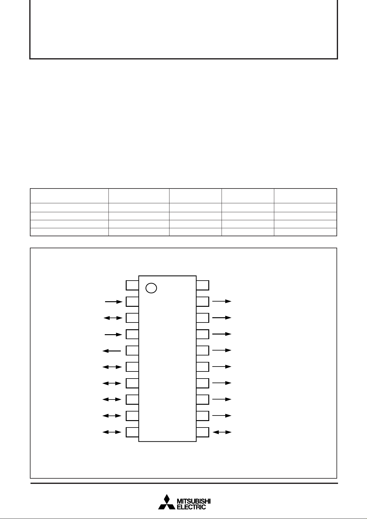
PIN CONFIGURATION (TOP VIEW)
M34280M1-XXXFP/GP
V
X
SS
E
E
X
IN
OUT
E
G
G
G
G
2
1
0
0
1
2
3
1
2
3
4
5
6
7
8
9
10
DD
20
19
V
CARR
M34280M1-XXXFP/GP
D
D
D
D
D
D
D
D
0
1
2
3
4
5
6
7
18
17
16
15
14
13
12
11
Outline 20P2N-A
20P2E/F-A
Page 2
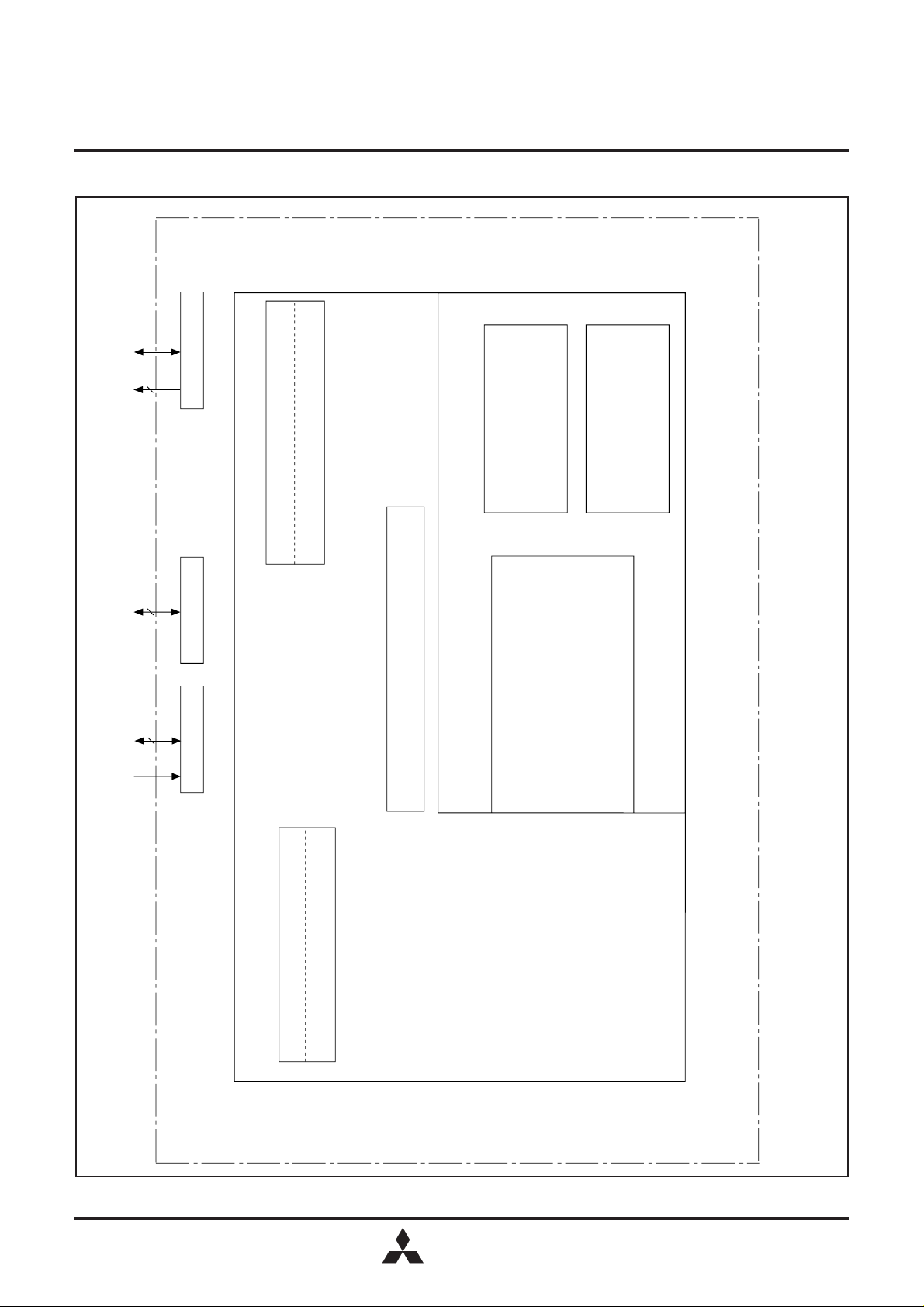
SINGLE-CHIP 4-BIT CMOS MICROCOMPUTER for INFRARED REMOTE CONTROL TRANSMITTERS
X
IN
–X
OUT
1
4
2
7
1
I/O port
Internal peripheral functions
Timer
System clock generating circuit
Remote control carrier wave output
Memory
ROM (Note)
1024 words × 9 bits
RAM
32 words × 4 bits
720 Series
CPU core
ALU (4 bits)
Register A (4 bits) Register B (4 bits)
Register D (3 bits) Register E (8 bits)
Stack register SK (4 levels)
Port E Port G Port D
Timer 1 (8 bits)
Note: PROM 1024 words × 9 bits
BLOCK DIAGRAM
MITSUBISHI MICROCOMPUTERS
4280 Group
2
MITSUBISHI
ELECTRIC
Page 3
SINGLE-CHIP 4-BIT CMOS MICROCOMPUTER for INFRARED REMOTE CONTROL TRANSMITTERS
PERFORMANCE OVERVIEW
Parameter
Number of basic instructions
Minimum instruction execution time
Memory sizes
Input/Output
ports
Timer 1
Subroutine nesting
Device structure
Package
Operating temperature range
Supply voltage
Power
dissipation
(typical value)
ROM
RAM
D0–D6
D7
E0–E2
E0, E1
G0–G3
CARR
Active mode
RAM back-up mode
M34280M1/
E1
Output
I/O
Input
Output
I/O
Output
MITSUBISHI MICROCOMPUTERS
4280 Group
Function
62
8.0 µs (at 4.0 MHz system clock frequency)
(f(X
IN) = 4.0 MHz, system clock = f(XIN)/8, VDD = 3 V)
1024 words ✕ 9 bits
32 words ✕ 4 bits
Seven independent output ports
1-bit I/O port with the pull-down function
3-bit input port with the pull-down function
2-bit output port (E0, E1)
4-bit I/O port with the pull-down function
1-bit output port; CMOS output
8-bit timer with a reload register
4 levels (However, only 3 levels can be used when the TABP p instruction is executed)
CMOS silicon gate
20-pin plastic molded SOP (20P2N-A)/SSOP (20P2E/F-A)
–20 °C to 85 °C
1.8 V to 3.6 V
400 µA
(f(X
IN) = 4.0 MHz, system clock = f(XIN)/8, VDD = 3 V)
0.1
µ
A (at room temperature, VDD = 3 V)
PIN DESCRIPTION
Name
Power supply
Ground
System clock input
System clock output
Output port D
I/O port D
I/O port E
I/O port G
Carrier wave output
for remote control
V
DD
VSS
XIN
XOUT
D0–D6
D7
E0–E2
G0–G3
CARR
Pin
Input/Output
—
—
Input
Output
Output
I/O
Output
Input
I/O
Output
Function
Connected to a plus power supply.
Connected to a 0 V power supply.
I/O pins of the system clock generating circuit. Connect a ceramic resonator
between pins X
and XOUT.
Each pin of port D has an independent 1-bit wide output function. The output
structure is P-channel open-drain.
1-bit I/O port. For input use, turn on the built-in pull-down transistor and set the
latch of the specified bit to “0.” In addition, key-on wakeup function using “H”
level sense becomes valid. The output structure is P-channel open-drain.
2-bit (E
0, E1) output port. The output structure is P-channel open-drain.
3-bit input port. For input use (E
set the latch of the specified bit to “0.” In addition, key-on wakeup function using
“H” level sense becomes valid. Port E2 has an input-only port and has a key-on
wakeup function using “H” level sense and pull-down transistor.
4-bit I/O port. For input use, set the latch of the specified bit to “0.” The output
structure is P-channel open-drain. Port G has a key-on wakeup function using
“H” level sense and pull-down transistor.
Carrier wave output pin for remote control. The output structure is CMOS circuit.
IN and XOUT. The feedback resistor is built-in between pins XIN
0, E1), turn on the built-in pull-down transistor and
MITSUBISHI
ELECTRIC
3
Page 4
MITSUBISHI MICROCOMPUTERS
4280 Group
SINGLE-CHIP 4-BIT CMOS MICROCOMPUTER for INFRARED REMOTE CONTROL TRANSMITTERS
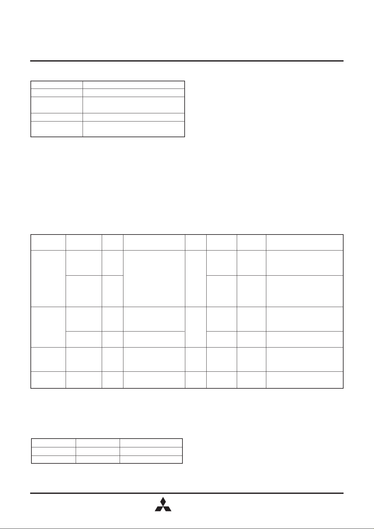
CONNECTIONS OF UNUSED PINS
Pin
D
0–D7
E0, E1
Open or connect to V
Set the output latch to “1” and open, or
connect to VDD pin (Note 2).
E2
G0–G3
Open or connect to V
Set the output latch to “0” and open, or
connect to VSS pin.
Notes 1: Port D7: Set the bit 2 (PU02) of the pull-down control register PU0 to “0” by software and turn the pull-down transistor OFF.
2: Set the corresponding bits (PU0
transistor OFF.
(Note in order to set the output latch to “0” to make pins open)
• After system is released from reset, a port is in a high-impedance state until the output latch of the port is set to “0” by software.
Accordingly, the voltage level of pins is undefined and the excess of the supply current may occur.
• To set the output latch periodically is recommended because the value of output latch may change by noise or a program run away
(caused by noise).
Connection
DD pin (Note 1).
SS pin.
0, PU01) of the pull-down control register PU0 to “0” by software and turn the pull-down
(Note when connecting to V
SS and VDD)
• Connect the unused pins to V
PORT FUNCTION
Port
Port D
Port E
Port G
Port CARR
0–D6
D
D7
E0
E1
E2
G0–G3
CARR
Pin
SS or VDD at the shortest distance and use the thick wire against noise.
Input/
Output
Output
(7)
Output structure
P-channel open-drain
Control
bits
1 bit
Control
instructions
SD
RD
Control
registers
CLD
I/O
(1)
SD
RD
PU0
CLD
SZD
I/O
P-channel open-drain
(2)
Output:
2 bits
OEA
IAE
PU0
Input:
Input
3 bits
IAE
(1)
I/O
(4)
Output
P-channel open-drain
CMOS
4 bits
1 bit
OGA
IAG
OCRA
C
(1)
Remark
Pull-down function and key-on
wakeup function
(programmable)
Pull-down function and key-on
wakeup function
(programmable)
Pull-down function and key-on
wakeup function
DEFINITION OF CLOCK AND CYCLE
• System clock (STCK)
The system clock is the source clock for controlling this product.
It can be selected as shown below whether to use the CCK
instruction.
CCK instruction
When not using
When using
4
System clock
f(X
IN)/8
IN)
f(X
Instruction clock
f(X
IN)/32
IN)/4
f(X
• Instruction clock (INSTCK)
The instruction clock is a signal derived by dividing the system
clock by 4, and is the basic clock for controlling CPU. The one
instruction clock cycle is equivalent to one machine cycle.
• Machine cycle
The machine cycle is the cycle required to execute the
instruction.
MITSUBISHI
ELECTRIC
Page 5
SINGLE-CHIP 4-BIT CMOS MICROCOMPUTER for INFRARED REMOTE CONTROL TRANSMITTERS
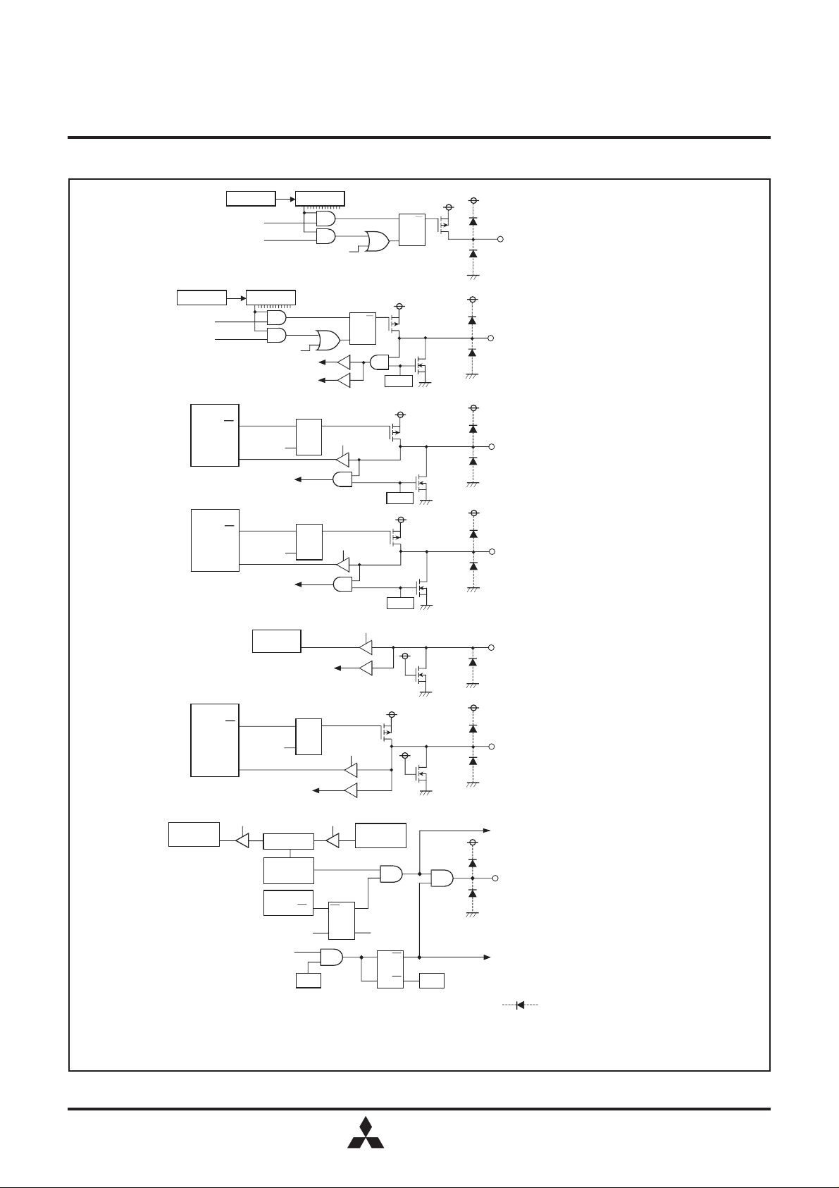
PORT BLOCK DIAGRAMS
MITSUBISHI MICROCOMPUTERS
4280 Group
Register Y Decoder
SD instruction
RD instruction
Register Y Decoder
SD instruction
RD instruction
Skip decision (SZD instruction)
Register A
Register A
CLD instruction
Key-on wakeup input
A
0
A
0
Key-on wakeup input
A
1
A
1
Key-on wakeup input
OEA
instruction
OEA
instruction
CLD instruction
Q
D
IAE instruction
T
Q
D
IAE instruction
T
S
Q
R
S
Q
R
Pull-down
transistor
PU0
2
Pull-down
transistor
PU0
0
Pull-down
transistor
PU0
1
(Note 1)
Ports D
(Note 1)
Port D7 (Note 4)
(Note 1)
Port E
(Note 1)
Port E
0–D6
0
(Note 4)
1
(Note 4)
Key-on wakeup input
Register A
A
i
(Note 2)
instruction
A
i
Key-on wakeup input
Register A
A
j
TAC instruction
(Note 3)
OCRA instruction
Timer 1 underflow signal
Register A
OGA
Register C
Carrier wave
output circuit
Register A
A
2
D
Q
T
IAG instruction
TCA instruction
A
3
V1
2
IAE instruction
Register A
A
j
(Note 3)
Q
D
TCA
R
T
instruction
2
(Note 4)
Port E
Pull-down
transistor
Pull-down
transistor
To timer 1
D
Q
R
V1
T
0
(Note 1)
(Note 1)
(Note 1)
Notes 1:
0–G3
Ports G
CARRY
Port CARR
Carrier wave
output control
signal
(Note 4)
This symbol represents a parasitic diode.
2:
i represents bits 0 to 3.
3:
j represents bits 0 to 2.
4:
Applied voltage must be less than V
DD
.
MITSUBISHI
ELECTRIC
5
Page 6
SINGLE-CHIP 4-BIT CMOS MICROCOMPUTER for INFRARED REMOTE CONTROL TRANSMITTERS
FUNCTION BLOCK OPERATIONS
CPU
(1) Arithmetic logic unit (ALU)
The arithmetic logic unit ALU performs 4-bit arithmetic such
as 4-bit data addition, comparison, and bit manipulation.
(CY)
(M(DP))
MITSUBISHI MICROCOMPUTERS
4280 Group
<Carry>
Addition
ALU
(2) Register A and carry flag
Register A is a 4-bit register used for arithmetic, transfer,
exchange, and I/O operation.
Carry flag CY is a 1-bit flag that is set to “1” when there is a
carry with the AMC instruction (Figure 1).
It is unchanged with both A n instruction and AM instruction.
The value of A
instruction (Figure 2).
Carry flag CY can be set to “1” with the SC instruction and
cleared to “0” with the RC instruction.
(3) Registers B and E
Register B is a 4-bit register used for temporary storage of 4bit data, and for 8-bit data transfer together with register A.
Register E is an 8-bit register. It can be used for 8-bit data
transfer with register B used as the high-order 4 bits and
register A as the low-order 4 bits (Figure 3).
(4) Register D
Register D is a 3-bit register.
It is used to store a 7-bit ROM address together with register
A and is used as a pointer within the specified page when the
TABP p, BLA p, or BMLA p instruction is executed (Figure 4).
0 is stored in carry flag CY with the RAR
(A)
<Result>
Fig. 1 AMC instruction execution example
<Set>
SC instruction
<Clear>
RC instruction
CY A3 A2 A1 A0
<Rotation>
RAR instruction
A0 CY A3 A2 A1
Fig. 2 RAR instruction execution example
Register B Register A
B3B2B1B
TAB instruction
0
A3A2A1A
TEAB instruction
Register E
ER7ER6ER5ER4ER3ER2ER1ER
0
0
TABP p instruction
Specifying address
PCH
p3 p2 p1 p0
Immediate field
value p
Fig. 4 TABP p instruction execution example
DR2 DR1DR0
The contents
of register D
PCL
A3 A2 A1 A0
The contents
of register A
B3B2B1B
Register B Register A
Fig. 3 Registers A, B and register E
ROM
8
40
Low-order 4 bits
Middle-order 4 bits
Most significant 1 bit
URS flag (1)
URSC instruction
TABE instruction
0
A3A2A1A
TBA instruction
Register A (4)
Register B (4)
Carry flag CY (1)
0
6
ELECTRIC
MITSUBISHI
Page 7
SINGLE-CHIP 4-BIT CMOS MICROCOMPUTER for INFRARED REMOTE CONTROL TRANSMITTERS
(5) Most significant ROM code reference enable flag (URS)
URS flag controls whether to refer to the contents of the most
significant 1 bit (bit 8) of ROM code when executing the TABP
p instruction. If URS flag is “0,” the contents of the most
significant 1 bit of ROM code is not referred even when
executing the TABP p instruction. However, if URS flag is “1,”
the contents of the most significant 1 bit of ROM code is set to
flag CY when executing the TABP p instruction (Figure 4).
URS flag is “0” after system is released from reset and returned
from RAM back-up mode. It can be set to “1” with the URSC
instruction, but cannot be cleared to “0.”
(6) Stack registers (SKs) and stack pointer (SP)
Stack registers (SKs) are used to temporarily store the contents
of program counter (PC) just before branching until returning
to the original routine when;
• performing a subroutine call, or
• executing the table reference instruction (TABP p).
Stack registers (SKs) are four identical registers, so that
subroutines can be nested up to 4 levels. However, one of
stack registers is used when executing a table reference
instruction. Accordingly, be careful not to over the stack. The
contents of registers SKs are destroyed when 4 levels are
exceeded.
The register SK nesting level is pointed automatically by 2-bit
stack pointer (SP).
Figure 5 shows the stack registers (SKs) structure.
Figure 6 shows the example of operation at subroutine call.
MITSUBISHI MICROCOMPUTERS
4280 Group
Program counter (PC)
Executing BM
instruction
Stack pointer (SP) points “3” at reset or
returning from RAM back-up mode. It points “0”
by executing the first BM instruction, and the
contents of program counter is stored in SK
When the BM instruction is executed after four
stack registers are used ((SP) = 3), (SP) = 0
and the contents of SK
Fig. 5 Stack registers (SKs) structure
Executing RT
instruction
SK0
SK1
SK2
SK3
0 is destroyed.
(SP) 0
(SK0) 000116
(PC) SUB1
(SP) = 0
(SP) = 1
(SP) = 2
(SP) = 3
0.
(7) Skip flag
Skip flag controls skip decision for the conditional skip
instructions and continuous described skip instructions.
Note : The 4280 Group just invalidates the next instruction
when a skip is performed. The contents of program
counter is not increased by 2. Accordingly, the number
of cycles does not change even if skip is not performed.
However, the cycle count becomes “1” if the TABP p,
RT, or RTS instruction is skipped.
Main program
Address
16 NOP
0000
16 BM SUB1
0001
Subroutine
SUB1 :
000216 NOP
(PC) (SK0)
(SP) 3
Note:
Returning to the BM instruction execution
address with the RT instruction, and the BM
instruction is equivalent to the NOP instruction.
Fig. 6 Example of operation at subroutine call
NOP
·
·
·
RT
MITSUBISHI
ELECTRIC
7
Page 8
MITSUBISHI MICROCOMPUTERS
4280 Group
SINGLE-CHIP 4-BIT CMOS MICROCOMPUTER for INFRARED REMOTE CONTROL TRANSMITTERS
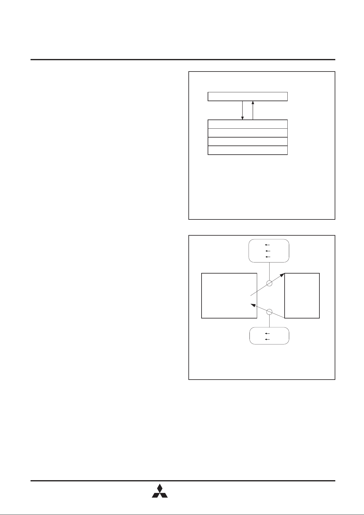
(8) Program counter (PC)
Program counter (PC) is used to specify a ROM address (page
and address). It determines a sequence in which instructions
stored in ROM are read. It is a binary counter that increments
the number of instruction bytes each time an instruction is
executed. However, the value changes to a specified address
when branch instructions, subroutine call instructions, return
instructions, or the table reference instruction (TABP p) is
executed.
Program counter consists of PC
which specifies to a ROM page and PC
specifies an address within a page. After it reaches the last
address (address 127) of a page, it specifies address 0 of the
next page (Figure 7).
Make sure that the PC
the built-in ROM.
(9) Data pointer (DP)
Data pointer (DP) is used to specify a RAM address and
consists of registers X and Y. Register X specifies a file and
register Y specifies a RAM digit (Figure 8).
Register Y is also used to specify the port D bit position.
When using port D, set the port D bit position to register Y
certainly and execute the SD, RD, or SZD instruction (Figure
9).
H does not exceed after the last page of
H (most significant bit to bit 7)
L (bits 6 to 0) which
Fig. 7 Program counter (PC) structure
Register X (2)
Program counter (PC)
p3p2p1p0a6a5a4a3a2a1a
PC
H
Specifying
PC
L
Specifying address
page
Data pointer (DP)
X1 X0 Y3 Y2 Y1 Y0
Register Y (4)
Specifying
RAM digit
Specifying RAM file
0
Fig. 8 Data pointer (DP) structure
Specifying bit position
Set
D5D7
1
01
0
Register Y (4)
Fig. 9 SD instruction execution example
1
Port D output latch
D0
8
ELECTRIC
MITSUBISHI
Page 9
MITSUBISHI MICROCOMPUTERS
4280 Group
SINGLE-CHIP 4-BIT CMOS MICROCOMPUTER for INFRARED REMOTE CONTROL TRANSMITTERS
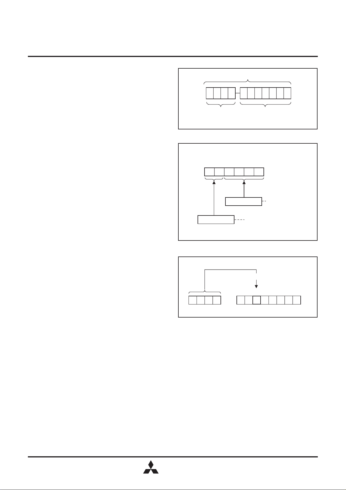
PROGRAM MEMORY (ROM)
The program memory is a mask ROM. 1 word of ROM is
composed of 9 bits. ROM is separated every 128 words by the
unit of page (addresses 0 to 127).
Table 1 ROM size and pages
Product
M34280M1
M34280E1
Page 2 (addresses 0100
subroutine calls. Subroutines written in this page can be called
from any page with the 1-word instruction (BM). Subroutines
extending from page 2 to another page can also be called with
the BM instruction when it starts on page 2.
ROM pattern of all addresses can be used as data areas with
the TABP p instruction.
ROM size (✕ 9 bits)
1024 words
16 to 017F16) is the special page for
Pages
8 (0 to 7)
DATA MEMORY (RAM)
1 word of RAM is composed of 4 bits, but 1-bit manipulation
(with the SB j, RB j, and SZB j instructions) is enabled for the
entire memory area. A RAM address is specified by a data
pointer. The data pointer consists of registers X and Y. Set a
value to the data pointer certainly when executing an instruction
to access RAM.
Table 2 shows the RAM size. Figure 12 shows the RAM map.
Table 2 RAM size
Product
M34280M1
M34280E1
32 words ✕ 4 bits (128 bits)
RAM size
16
0000
007
F16
008016
00FF16
010016
017F16
Subroutine special page
018016
03FF16
Fig. 10 ROM map of M34280M1
RAM 32 words × 4 bits (128 bits)
Register X
0
1
2
3
4
5
Register Y
6
7
087654321
Page 0
Page 1
Page 2
Page 3
Page 7
23
0
1
Fig. 11 RAM map
32 words
MITSUBISHI
ELECTRIC
9
Page 10
SINGLE-CHIP 4-BIT CMOS MICROCOMPUTER for INFRARED REMOTE CONTROL TRANSMITTERS
TIMERS
The 4280 Group has the programmable timer.
• Programmable timer
The programmable timer has a reload register and enables
the frequency dividing ratio to be set. It is decremented from a
setting value n. When it underflows (count to n + 1), a timer 1
underflow flag is set to “1,” new data is loaded from the reload
register, and count continues (auto-reload function).
FF16
n : Counter initial value
Count starts
MITSUBISHI MICROCOMPUTERS
4280 Group
Reload Reload
n
The contents of counter
0016
Timer 1 underflow flag
Fig. 12 Auto-reload function
1st underflow 2nd underflow
Time
n+1 count n+1 count
A skip instruction is executed.
10
MITSUBISHI
ELECTRIC
Page 11
SINGLE-CHIP 4-BIT CMOS MICROCOMPUTER for INFRARED REMOTE CONTROL TRANSMITTERS
The 4280 Group timer consists of the following circuit.
• Timer 1 : 8-bit programmable timer
This timer can be controlled with the timer control register V1.
Timer 1 function is described below.
Table 3 Function related timer
Circuit
Timer 1
Structure
8-bit programmable
binary down counter
Count source
• Carrier generating circuit
output (CARRY)
• Bit 5 of watchdog timer
Frequency
dividing ratio
1 to 256
MITSUBISHI MICROCOMPUTERS
4280 Group
Use of output signal
• Carrier wave output control
Control
register
V1
CARRY
XIN
CCK instruction
Initializing signal
V1
1
0
1
(Note 3)
INSTCK
V1
0
(Note 1)
0
1
(TAB1)
Frequency
divider
(divided by 8)
S
Q
R
Timer 1 (8)
Reload register R1 (8)
(T1AB)
Register B
Synchronous
circuit
Initializing signal
14-bit timer (WDT)
5
(Note 2)
Register A
(Note 3)
130
SNZT1 instruction
V1
2
STCK (System clock)
Frequency
divider
(divided by 4)
WDF1 WDF2
T1F
D
T
Q
V1
R
(Instruction clock)
System reset
Carrier wave output control signal
0
INSTCK
Fig. 13 Timers structure
WRST instruction
Initializing signal
(Note 3)
Notes 1: Counting is stopped by clearing to “0.”
2: When the T1AB instruction is executed after V1
writing is performed only to reload register R1.
3: The initializing signal is output at reset or RAM back-up mode.
: Data is automatically set from a reload register
when timer 1 underflows (auto-reload function).
0
is set to “1,”
MITSUBISHI
ELECTRIC
11
Page 12

SINGLE-CHIP 4-BIT CMOS MICROCOMPUTER for INFRARED REMOTE CONTROL TRANSMITTERS
Table 4 Control registers related to timer
MITSUBISHI MICROCOMPUTERS
4280 Group
Timer control register V1
V1
V11
V10
Note: “W” represents write enabled.
(1) Control register related to timer
• Timer control register V1
(2) Precautions
Note the following for the use of timers.
• Count source
• Watchdog timer
• Writing to reload register R1
Carrier wave output auto-control bit
2
Timer 1 count source selection bit
Timer 1 control bit
Register V1 controls the timer 1 count source and autocontrol function of carrier wave output from port CARR by
timer 1. Set the contents of this register through register A
with the TV1A instruction.
Stop timer 1 counting to change its count source.
Be sure that the timing to execute the WRST instruction in
order to operate WDT efficiently.
When writing data to reload register R1 while timer 1 is
operating, avoid a timing when timer 1 underflows.
at reset : 0002 Wat RAM back-up : 0002
Auto-control output by timer 1 is invalid
0
Auto-control output by timer 1 is valid
1
Carrier output (CARRY)
0
Bit 5 of watchdog timer (WDT)
1
Stop (Timer 1 state retained)
0
Operating
1
(4) Timer 1 underflow flag (T1F)
Timer 1 underflow flag is set to “1” when the timer 1 underflows.
The state of this flag can be examined with the skip instruction
(SNZT1).
T1F flag is cleared to “0” when the next instruction is skipped
with a skip instruction.
(3) Timer 1
Timer 1 is an 8-bit binary down counter with the timer 1 reload
register (R1).
When timer is stopped, data can be set simultaneously in timer
1 and the reload register (R1) with the T1AB instruction.
When timer is operating, data can be set to only reload register
R1 with the T1AB instruction.
When setting the next count data to reload register R1 at
operating, set data before timer 1 underflows.
Timer 1 starts counting after the following process;
➀ set data in timer 1,
➁ select the count source with the bit 1 of register V1, and
➂ set the bit 0 of register V1 to “1.”
Once count is started, when timer 1 underflows (the next count
pulse is input after the contents of timer 1 becomes “0”), the
timer 1 underflow flag (T1F) is set to “1,” new data is loaded
from reload register R1, and count continues (auto-reload
function).
When a value set in reload register R1 is n, timer 1 divides the
count source signal by n + 1 (n = 0 to 255).
Data can be read from timer 1 to registers A and B. When
reading the data, stop the counter and then execute the TAB1
instruction.
12
MITSUBISHI
ELECTRIC
Page 13
SINGLE-CHIP 4-BIT CMOS MICROCOMPUTER for INFRARED REMOTE CONTROL TRANSMITTERS
WATCHDOG TIMER
Watchdog timer provides a method to reset and restart the system
when a program runs wild. Watchdog timer consists of 14-bit
timer (WDT) and watchdog timer flags (WDF1, WDF2).
Watchdog timer downcounts the instruction clock (INSTCK) as
the count source. When the timer WDT count value becomes
0000
16 and underflow occurs, the WDF1 flag is set to “1.” Then,
when the WRST instruction is not executed before the timer WDT
counts 16383, WDF2 flag is set to “1” and internal reset signal is
generated and system reset is performed.
When using the watchdog timer, execute the WRST instruction
at period of 16383 machine cycle or less to keep the
microcomputer operation normal.
Timer WDT is also used for generation of oscillation stabilization
time. When system is returned from reset and from RAM backup mode by key-input, software starts after the stabilization
oscillation time until timer WDT downcounts to 3E00
16 elapses.
MITSUBISHI MICROCOMPUTERS
4280 Group
3FFF16
3E0016
Value of timer WDT
0000 16
WDF1 flag
WDF2 flag
Internal reset signal
System reset Return
Fig. 14 Watchdog timer function
“1”
“0”
“1”
“0”
“H”
“L”
Software
start
POF
instruction
execution
Software
start
WRST
instruction
execution
Software
start
System reset
MITSUBISHI
ELECTRIC
13
Page 14
MITSUBISHI MICROCOMPUTERS
4280 Group
SINGLE-CHIP 4-BIT CMOS MICROCOMPUTER for INFRARED REMOTE CONTROL TRANSMITTERS
CARRIER GENERATING CIRCUIT
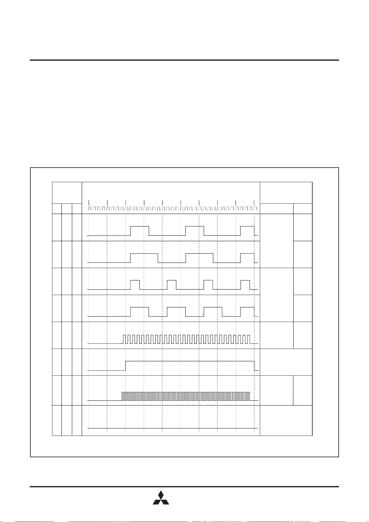
The 4280 Group can output the various carrier waveforms by
the carrier wave selection register C.
Set the contents of this register through register A with the TCA
instruction. The TAC instruction can be used to transfer the
contents of register C to register A. When the TCA instruction is
executed, the output latch of port CARR is cleared to “0.”
The carrier waveform selected by setting register C can be output
from port CARR by setting port CARR output latch to “1.” When
the CARR output latch is cleared to “0,” carrier wave output is
stopped and port CARR output is fixed to “L” level. The CARR
output latch can be set through bit 3 (A
OCRA instruction.
Carrier wave selection register C (at reset: 111
Register C
setting value
LA 8
1
C
C
2
C
0
0
0
0
0
“H”
“L”
“H”
1
0
“L”
3) of register A with the
OCRA
2
, at RAM back-up: 1112)
Output waveform
The relationship between the setting value of register C and
selected waveform is described below.
Also, timer 1 can auto-control the carrier wave output from port
CARR by setting the timer control register V1.
Carrier wave
Frequency
Duty
LA 0
(TCA)
OCRA
1/3
System clock/
12
1/2
0
0
1
1
1
1
Note: This carrier wave can be used only when system clock f(X
“L”
“H”
1
1
“L”
“H”
0
0
“L”
“H”
1
0
“L”
“H”
0
1
“L”
“H”
1
1
“L”
IN
)/8 is selected.
“H”
0
1
The carrier wave output is fixed to “L” level when system clock f(X
IN
) is selected.
System clock/
8
System clock
No carrier wave
f(XIN)/4
(Note)
“L” level fixed
1/4
1/2
1/2
1/2
Fig. 15 Carrier wave selection register
14
MITSUBISHI
ELECTRIC
Page 15
MITSUBISHI MICROCOMPUTERS
4280 Group
SINGLE-CHIP 4-BIT CMOS MICROCOMPUTER for INFRARED REMOTE CONTROL TRANSMITTERS
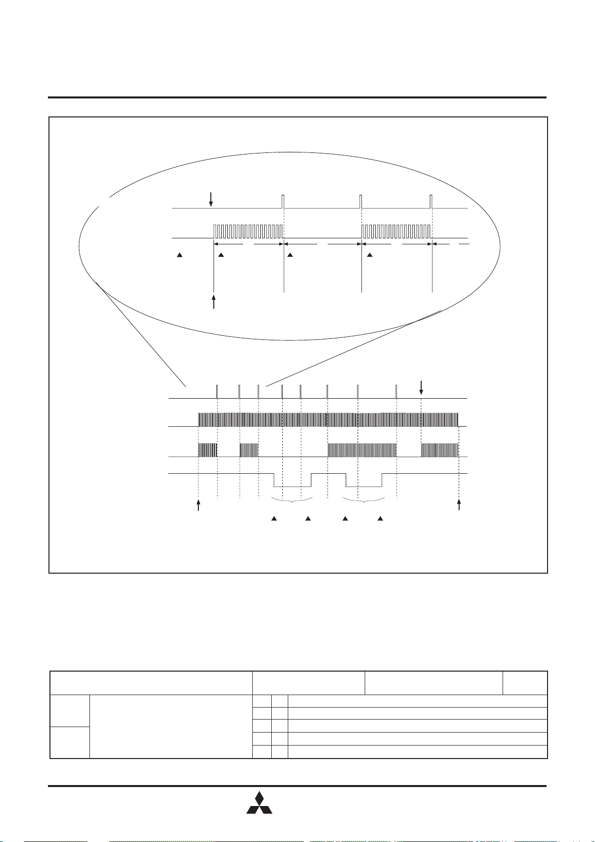
Timer 1 start
(V1
0)←1
a
a
b
b
cd
c d
Timer 1 underflow
Port CARR output
“1”
“0”
“H”
“L”
Set the interval “a” to timer 1.
Select count source CARRY
Timer 1 underflow
Port CARR output
Register V12
(V11)←0
Auto-control valid
(V1
CARRY
2)←1
“1”
“0”
“H”
“L”
“H”
“L”
“1”
“0”
Carrier wave output start
Set the interval “b”
to reload register R1.
Carrier wave output start
Set the interval “c”
to reload register R1.
Auto-control invalid Auto-control invalid
2)←0 (V12)←1 (V12)←0 (V12)←1
(V1
Set the interval “d”
to reload register R1.
Timer 1 stop
0)←0
(V1
(Note)
Carrier wave output stop
Note: When timer 1 is stopped, the port CARR output auto-control is terminated regardless of bit 2 (V12) of register V1.
Fig. 16 Port CARR output auto-control by timer 1
LOGIC OPERATION FUNCTION
The 4280 Group has the 4-bit logic operation function. The logic
operation between the contents of register A and the low-order 4
bits of register E is performed and its result is stored in register
A.
Each logic operation can be selected by setting logic operation
selection register LO.
Set the contents of this register through register A with the TLOA
instruction. The logic operation selected by register LO is
executed with the LGOP instruction.
Table 5 shows the logic operation selection register LO.
Table 5 Logic operation selection register LO
Logic operation selection register LO
LO1
Logic operation selection bits
LO0
at reset : 002 at RAM back-up : 002 W
L
O
1
O
0
L
0
0
Exclusive logic OR operation (XOR)
0
1
OR operation (OR)
1
0
AND operation (AND)
1
1
Not available
Logic operation function
Note: “W” represents write enabled.
MITSUBISHI
ELECTRIC
15
Page 16

MITSUBISHI MICROCOMPUTERS
4280 Group
SINGLE-CHIP 4-BIT CMOS MICROCOMPUTER for INFRARED REMOTE CONTROL TRANSMITTERS
RESET FUNCTION
The 4280 Group has the power-on reset circuit, though it does
not have RESET pin. System reset is performed automatically
at power-on, and software starts program from address 0 in page
0.
f(X
IN)
Internal reset signal
Fig. 17 Reset release timing
“H”
“L”
In order to make the built-in power-on reset circuit operate
efficiently, set the voltage rising time until V
obtained at power-on 1ms or less.
f(XIN) 16384 pulses
Software starts
DD= 0 to 2.2 V is
(address 0 in page 0)
Internal reset signal
Power-on reset circuit
Voltage drop detection circuit
Watchdog timer output
Fig. 18 Power-on reset circuit example
VDD
Power-on reset circuit
output voltage
Reset state
Internal reset signal
Reset released
Power-on
16
MITSUBISHI
ELECTRIC
Page 17

MITSUBISHI MICROCOMPUTERS
4280 Group
SINGLE-CHIP 4-BIT CMOS MICROCOMPUTER for INFRARED REMOTE CONTROL TRANSMITTERS
(1) Internal state at reset
Table 6 shows port state at reset, and Figure 19 shows internal
state at reset (they are retained after system is released from
reset).
• Program counter (PC) ..............................................................
Address 0 in page 0 is set to program counter.
• Power down flag (P).................................................................
• Timer 1 underflow flag (T1F) ...................................................
• Timer control register V1..........................................................
• Carrier wave selection register C ............................................
• Pull-down control register PU0 ................................................
• Logic operation selection register LO ......................................
• Most significant ROM code reference enable flag (URS)
• Carry flag (CY) .........................................................................
• Register A.................................................................................
• Register B.................................................................................
• Stack pointer (SP) ....................................................................
Fig. 19 Internal state at reset
Table 6 Port state at reset
Name
D
0–D6
D7
G0–G3, E2
E0, E1
Note: The contents of all output latch is initialized to “0.”
“H” output
“H” output
Input port (Pull-down transistor ON)
Input circuit OFF (Pull-down transistor OFF)
State at reset
The contents of timers, registers, flags and RAM except shown
in Figure 19 are undefined, so set the initial value to them.
0000000000
0
0
000
111
000
00
0
0
1111
1111
11
State after system is released from reset
High impedance state
Input circuit OFF (Pull-down transistor OFF)
Input port (Pull-down transistor ON)
Input port (Pull-down transistor OFF)
VOLTAGE DROP DETECTION CIRCUIT
The built-in drop detection circuit is designed to detect a drop in
voltage at operating and to reset the microcomputer if the supply
voltage drops below the specified value (Typ. 1.50 V) or less.
VDD
Reset voltage
Internal reset signal
Fig. 20 Voltage drop detection circuit operation waveform
The voltage drop detection circuit is stopped and power
dissipation is reduced at the RAM back-up mode, when the
functions except the RAM and pull-down control register (PU0)
are initialized.
Microcomputer starts operation
after f(X
IN) is counted to 16384 times.
MITSUBISHI
ELECTRIC
17
Page 18

MITSUBISHI MICROCOMPUTERS
4280 Group
SINGLE-CHIP 4-BIT CMOS MICROCOMPUTER for INFRARED REMOTE CONTROL TRANSMITTERS
RAM BACK-UP MODE
The 4280 Group has the RAM back-up mode.
When the POF instruction is executed, system enters the RAM
back-up state.
As oscillation stops retaining RAM, the function of reset circuit
and states at RAM back-up mode, power dissipation can be
reduced without losing the contents of RAM. Table 7 shows the
function and states retained at RAM back-up. Figure 21 shows
the state transition.
(1) Identification of the start condition
Warm start (return from the RAM back-up state) or cold start
(return from the normal reset state) can be identified by
examining the state of the power down flag (P) with the SNZP
instruction.
(2) Warm start condition
When the external wakeup signal is input after the system
enters the RAM back-up state by executing the POF
instruction, the CPU starts executing the software from address
0 in page 0. In this case, the P flag is “1.”
(3) Cold start condition
The CPU starts executing the software from address 0 in page
0 when any of the following conditions is satisfied .
• reset by power-on reset circuit is performed
• reset by watchdog timer is performed
• reset by voltage drop detection circuit is performed
In this case, the P flag is “0.”
Table 7 Functions and states retained at RAM back-up
Function
Program counter (PC), registers A, B,
carry flag (CY), stack pointer (SP) (Note 2)
Contents of RAM
Ports D
0–D6 (Note 3)
Port D
Port E0
Port E1
7
(PU02)=0 (Note 3)
(PU0
2)=1
0)=0 (Note 4)
(PU0
(PU0
0)=1
(PU0
1)=0 (Note 4)
1)=1
(PU0
Port G
Timer control register V1
Pull-down control register PU0
Logic operation selection register LO
Timer 1 function
Timer 1 underflow flag (T1F)
Watchdog timer (WDT)
Watchdog timer flag 1 (WDF1)
Watchdog timer flag 2 (WDF2)
Most significant ROM code reference enable flag (URS)
RAM back-up
✕
O
✕ (“H” output)
✕ (“H” output)
✕ (input)
✕ (input cut-off)
✕ (input)
✕ (input cut-off)
✕ (input)
✕ (input)
✕
O
✕
✕
✕
✕
✕
✕
✕
Notes 1: “O” represents that the function can be retained, and
“✕” represents that the function is initialized.
Registers and flags other than the above are undefined
at RAM back-up, and set an initial value after returning.
2:The stack pointer (SP) points the level of the stack
register and is initialized to “11
2” at RAM back-up.
3: The contents of port output latch is initialized to “0.”
However, port continues to output “H” level.
4: The state of this bit is equal to the state at reset.
18
MITSUBISHI
ELECTRIC
Page 19

SINGLE-CHIP 4-BIT CMOS MICROCOMPUTER for INFRARED REMOTE CONTROL TRANSMITTERS
(4) Return signal
An external wakeup signal is used to return from the RAM
back-up mode. Table 8 shows the return condition for each
return source.
Table 8 Return source and return condition
Return source
Ports D
7, E0, E1
Ports G, E2
Return by an external “H” level
input.
Return by an external “H” level
input.
Return condition
MITSUBISHI MICROCOMPUTERS
4280 Group
Remarks
Only key-on wakeup function of the port whose pull-down transistor is
turned ON is valid.
Key-on wakeup function is always valid.
(5) Pull-down control register PU0
• Pull-down control register PU0
Register PU0 controls the ON/OFF of pull-down transistor,
input, key-on wakeup function of ports E
Table 9 Pull-down control register
Pull-down control register PU0 at reset : 0002 at RAM back-up : state retained W
Port D
PU02
PU01
PU00
Note: “W” represents write enabled.
7 pull-down control bit
Port E1 pull-down control bit
Port E
0 pull-down control bit
0, E1 and D7.
(Stabilizing time a )
Reset
f(X
Pull-down transistor OFF, input circuit OFF, key-on wakeup invalid
0
Pull-down transistor ON, input circuit ON, key-on wakeup valid
1
Pull-down transistor OFF, key-on wakeup invalid
0
Pull-down transistor ON, key-on wakeup valid
1
Pull-down transistor OFF, key-on wakeup invalid
0
Pull-down transistor ON, key-on wakeup valid
1
A
IN) oscillation
Set the contents of this register through register A with the
TPU0A instruction.
POF instruction
B
is executed
IN) stop
f(X
Return input
(Stabilizing time a )
(RAM back-up
mode)
Stabilizing time a
Fig. 21 State transition
: Microcomputer starts its operation after f(XIN) is counted to16384 times.
Power down flag P
POF instruction
SRQ
Reset input
● Set source POF instruction is executed
● Clear source Reset input
Fig. 22 Set source and clear source of the P flag
Software start
P = “1”
?
Yes
No
Cold start
Fig. 23 Start condition identified example using the SNZP
instruction
Warm start
MITSUBISHI
ELECTRIC
19
Page 20

SINGLE-CHIP 4-BIT CMOS MICROCOMPUTER for INFRARED REMOTE CONTROL TRANSMITTERS
CLOCK CONTROL
The clock control circuit consists of the following circuits.
• System clock generating circuit
• Control circuit to stop the clock oscillation
• Control circuit to return from the RAM back-up state
MITSUBISHI MICROCOMPUTERS
4280 Group
CCK instruction
XIN
XOUT
POF instruction
Fig. 24 Clock control circuit structure
Clock signal f(X
resonator. Connect this external circuit to pins X
the shortest distance as shown Figure 26.
A feedback resistor is built-in between X
IN) is obtained by externally connecting a ceramic
OSC
R
Q
S
Frequency
divider
(divided by 8)
IN and XOUT at
IN pin and XOUT pin.
ROM ORDERING METHOD
Please submit the information described below when ordering
Mask ROM.
(1) Mask ROM Order Confirmation Form .................................1
(2) Data to be written into mask ROM.......................... EPROM
(three sets containing the identical data)
(3) Mark Specification Form .................................................... 1
Multiplexer
Internal clock
generating circuit
(divided by 4)
STCK
Internal power-on reset circuit
Pull-down control
register PU0
4280
X
IN
45
C
IN
X
OUT
C
OUT
INSTCK
Port D7
Ports E0, E1
Ports E2, G0–G3
Use the resonator
manufacturer’s
recommended value
because constants
such as capacitance
depend on the
resonator.
20
Fig. 25 Ceramic resonator external circuit
MITSUBISHI
ELECTRIC
Page 21

SINGLE-CHIP 4-BIT CMOS MICROCOMPUTER for INFRARED REMOTE CONTROL TRANSMITTERS
LIST OF PRECAUTIONS
➀ Noise and latch-up prevention
Connect a capacitor on the following condition to prevent noise
and latch-up;
• connect a bypass capacitor (approx. 0.01
V
DD and VSS at the shortest distance,
• equalize its wiring in width and length, and
• use the thickest wire.
In the One Time PROM version, port E
pin. Connect this pin to VSS through the resistor about 5 kΩ
which is assigned to E
shortest distance.
➁ Notes on unused pins
(Note in order to set the output latch to “0” to make pins open)
• After system is released from reset, a port is in a highimpedance state until the output latch of the port is set to
“0” by software.
Accordingly, the voltage level of pins is undefined and the
excess of the supply current may occur.
• To set the output latch periodically is recommended
because the value of output latch may change by noise or
a program run away (caused by noise).
2/VPP pin as close as possible at the
µ
F) between pins
2 is also used as VPP
MITSUBISHI MICROCOMPUTERS
4280 Group
(Note when connecting to V
• Connect the unused pins to V
distance and use the thick wire against noise.
➂ Timer
• Count source
Stop timer 1 counting to change its count source.
• Watchdog timer
Be sure that the timing to execute the WRST instruction in
order to operate WDT efficiently.
• Writing to reload register R1
When writing data to reload register R1 while timer 1 is
operating, avoid a timing when timer 1 underflows.
➃ Program counter
Make sure that the program counter does not specify after the
last page of the built-in ROM.
SS and VDD)
SS and VDD at the shortest
MITSUBISHI
ELECTRIC
21
Page 22

MITSUBISHI MICROCOMPUTERS
SINGLE-CHIP 4-BIT CMOS MICROCOMPUTER for INFRARED REMOTE CONTROL TRANSMITTERS
SYMBOL
The symbols shown below are used in the following list of instruction function and the machine instructions.
4280 Group
Symbol
A
B
DR
ER
C
V1
PU0
LO
X
Y
DP
PC
PC
H
PCL
SK
SP
CY
R1
T1
T1F
WDT
WDF1
WDF2
URS
P
STCK
INSTCK
Contents
Register A (4 bits)
Register B (4 bits)
Register D (3 bits)
Register E (8 bits)
Carrier wave selection register C (3 bits)
Timer control register V1 (3 bits)
Pull-down control register PU0 (3 bits)
Logic operation selection register LO (2 bits)
Register X (2 bits)
Register Y (4 bits)
Data pointer (6 bits)
(It consists of registers X and Y)
Program counter (10 bits)
High-order 3 bits of program counter
Low-order 7 bits of program counter
Stack register (10 bits ✕ 4)
Stack pointer (2 bits)
Carry flag
Timer 1 reload register
Timer 1
Timer 1 underflow flag
Watchdog timer
Watchdog timer flag 1
Watchdog timer flag 2
Most significant ROM code reference enable flag
Power down flag
System clock
Instruction clock
Symbol
D
E
G
CARR
x
y
p
n
j
A
3A2A1A0
←
↔
?
( )
—
M(DP)
a
p, a
C
+
x
Contents
Port D (8 bits)
Port E (3 bits)
Port G (4 bits)
Port CARR (1 bit)
Hexadecimal variable
Hexadecimal variable
Hexadecimal variable
Hexadecimal constant which represents the
immediate value
Hexadecimal constant which represents the
immediate value
Binary notation of hexadecimal variable A
(same for others)
Direction of data movement
Data exchange between a register and memory
Decision of state shown before “?”
Contents of registers and memories
Negate, Flag unchanged after executing
instruction
RAM address pointed by the data pointer
Label indicating address a
Label indicating address a6 a5 a4 a3 a2 a1 a0
in page p3 p2 p1 p0
Hex. number C + Hex. number x (also same for
others)
6 a5 a4 a3 a2 a1 a0
Note : The 4280 Group just invalidates the next instruction when a skip is performed. The contents of program counter is not
increased by 2. Accordingly, the number of cycles does not change even if skip is not performed. However, the cycle count
becomes “1” if the TABP p, RT, or RTS instruction is skipped.
MITSUBISHI
22
ELECTRIC
Page 23

SINGLE-CHIP 4-BIT CMOS MICROCOMPUTER for INFRARED REMOTE CONTROL TRANSMITTERS
LIST OF INSTRUCTION FUNCTION
Grouping Mnemonic
TAB
TBA
TAY
TYA
TEAB
(A) ← (B)
(B) ← (A)
(A) ← (Y)
(Y) ← (A)
(ER
(ER
TABE
Register to register transfer
TDA
LXY x, y
(B) ← (ER7–ER4)
(A) ← (ER
(DR
(X) ← x, x = 0 to 3
(Y) ← y, y = 0 to 15
INY
DEY
TAM j
(Y) ← (Y) + 1
(Y) ← (Y) – 1
(A) ← (M(DP))
(X) ← (X) EXOR(j)
j = 0 to 3
XAM j
(A) ←→ (M(DP))
(X) ← (X) EXOR(j)
j = 0 to 3
XAMD j
(A) ←→ (M(DP))
(X) ← (X) EXOR(j)
j = 0 to 3
(Y) ← (Y) – 1
XAMI j
(A) ←→ (M(DP))
(X) ← (X) EXOR(j)
j = 0 to 3
RAM to register transfer RAM addresses
(Y) ← (Y) + 1
Function
7–ER4) ← (B)
3–ER0) ← (A)
3–ER0)
2–DR0) ← (A2–A0)
Grouping
Mnemonic
LA n
(A) ← n
n = 0 to 15
TABP p
(SP) ← (SP) + 1
(SK(SP)) ← (PC)
(PCH) ← p p=0 to 7
(PC
3–A0)
A
When URS=0
(B) ← (ROM(PC))
(A) ← (ROM(PC))3 to 0
When URS=1
(CY) ← (ROM(PC))
(B) ← (ROM(PC))7 to 4
(A) ← (ROM(PC))3 to 0
(PC) ← (SK(SP))
(SP) ← (SP) – 1
AM
AMC
Arithmetic operation
(A) ← (A) + (M(DP))
(A) ← (A) + (M(DP))
+ (CY)
(CY) ← Carry
A n
(A) ← (A) + n
n = 0 to 15
SC
RC
SZC
CMA
RAR
LGOP
(CY) ← 1
(CY) ← 0
(CY) = 0 ?
(A) ← (A)
→ CY → A
Logic operation
instruction
XOR, OR, AND
Function
L) ← (DR2–DR0,
7 to 4
8
3A2A1A0
MITSUBISHI MICROCOMPUTERS
4280 Group
Grouping
Mnemonic
SEAM
SEA n
operation
Comparison
B a
BL p, a
BA a
Branch operation
BLA p, a
BM a
BML p, a
Subroutine operation
BMLA p,
a
RT
RTS
Return operation
Function
(A) = (M(DP)) ?
(A) = n ?
n = 0 to 15
(PC
L) ← a6–a0
(PCH) ← p
(PC
L) ← a6–a0
(PCL) ← (a6–a4,
(PCH) ← p
(PC
L) ← (a6–a4, A3–A0)
(SP) ← (SP) + 1
(SK(SP)) ← (PC)
(PCH) ← 2
(PC
L) ← a6–a0
(SP) ← (SP) + 1
(SK(SP)) ← (PC)
(PC
H) ← p p= 0 to 7
L) ← a6–a0
(PC
(SP) ← (SP) + 1
(SK(SP)) ← (PC)
(PC
H) ← p p= 0 to 7
L) ← (a6–a4, A3–A0)
(PC
(PC) ← (SK(SP))
(SP) ← (SP) – 1
(PC) ← (SK(SP))
(SP) ← (SP) – 1
A3–A
0)
SB j
RB j
Bit operation
SZB j
(Mj(DP)) ← 1
j = 0 to 3
(Mj(DP)) ← 0
j = 0 to 3
(Mj(DP)) = 0 ?
j = 0 to 3
MITSUBISHI
ELECTRIC
23
Page 24

SINGLE-CHIP 4-BIT CMOS MICROCOMPUTER for INFRARED REMOTE CONTROL TRANSMITTERS
LIST OF INSTRUCTION FUNCTION (CONTINUED)
Grouping
Mnemonic
TV1A
Function
(V1
2–V10) ← (A2–A0)
Grouping
Mnemonic
NOP
(PC) ← (PC) + 1
MITSUBISHI MICROCOMPUTERS
4280 Group
Function
TAB1
T1AB
Timer operation
SNZ1
TCA
TAC
Carrier wave
OCRA
control operation
(B) ← (T17–T14)
(A) ← (T1
3–T10)
at timer 1 stop (V10=0):
(R1
7–R14) ← (B)
7–T14) ← (B)
(T1
(R1
3–R10) ← (A)
(T1
3–T10) ← (A)
at timer 1 operating:
(V10=1)
7–R14) ← (B)
(R1
(R1
3–R10) ← (A)
(T1F) = 1 ?
After skipping the next
instruction
(T1F) ← 0
(C
2–C0) ← (A2–A0)
(CARR) ← 0
(A
2–A0) ← (C2–C0)
(CARR) ← (A3)
POF
SNZP
CCK
TLOA
URSC
Other operation
TPU0A
WRST
RAM back-up
(P) = 1 ?
STCK
changes to f(XIN)
(LO1, LO0) ← (A1, A0)
(URS) ← 1
(
PU02–PU0
0) ← (A2–A0)
(WDF1) ← 0
CLD
RD
(D) ← 1
(D(Y)) ← 0
(Y) = 0 to 7
SD
(D(Y)) ← 1
(Y) = 0 to 7
SZD
(D(Y)) = 0 ?
(Y) = 7
OEA
(E
1, E0) ← (A1, A0)
Input/Output operation
IAE
OGA
IAG
(A2–A0) ← (E2–E0)
(G) ← (A)
(A) ← (G)
24
MITSUBISHI
ELECTRIC
Page 25

MITSUBISHI MICROCOMPUTERS
4280 Group
SINGLE-CHIP 4-BIT CMOS MICROCOMPUTER for INFRARED REMOTE CONTROL TRANSMITTERS
INSTRUCTION CODE TABLE
LXY
3,0
LXY
3,1
LXY
3,2
LXY
3,3
LXY
3,4
LXY
3,5
LXY
3,6
LXY
3,7
LXY
3,8
LXY
3,9
LXY
3,10
LXY
3,11
LXY
3,12
LXY
3,13
LXY
3,14
LXY
3,15
10000 11000
10111 11111
18–1F
10–17
B
BM
BM B
B
BM
B
BM
B
BM
BM
B
BM
B
B
BM
B
BM
BM B
B
BM
B
BM
BM B
B
BM
B
BM
B
BM
D3–
0
D
0000
0001
0010
0011
0100
0101
0110
0111
1000
1001
1010
1011
1100
1101
1110
1111
00000 00001 00010 00011
D8–D
4
Hex.
00 01 02 03 04 05 06 07 08 09 0A 0B 0C 0D 0E 0F
notation
NOP
BA
SNZP
RC
SC
AM
AMC
TYA
POF
TBA
WRST
BLA
CLD
INY
SD
DEY
TEAB
CMA
RAR
TAB
TAY
0
1
2
3
4
5
6
7
8
9
A
B
C
D
E
F
RD
SZB
0
SZB
1
SZB
2
SZB
3
SZD
SEAn
SEAM
IAG
TDA
TABE
SZC
00100 00101 00110 00111
BL TAC
BL
BL
BL
BL
BL
BL
BL
BMLA
LGOP
SNZT1
RT
RTS
IAE
T1AB TAB1
TLOA
CCK
TCA
TV1A
SB
RB
0
0
SB
RB
1
1
SB
RB
2
2
SB
RB
3
3
XAM
0
XAM
1
XAM
2
XAM
3
TAM
0
TAM
1
TAM
2
TAM
3
XAMI
0
XAMI
1
XAMI
2
XAMI
3
XAMD
0
XAMD
1
XAMD
2
XAMD
3
01000 01001 01010 01011 01100 01101 01110 01111
BML
BML
BML
BML
BML
BML
BML
BML
OGA
URSC
OEA
OCRA
TPU0A
TABP
0
TABP
1
TABP
2
TABP
3
TABP
4
TABP
5
TABP
6
TABP
7
A
0
A
1
A
2
A
3
A
4
A
5
A
6
A
7
A
8
A
9
A
10
A
11
A
12
A
13
A
14
A
15
LA
0
LA
1
LA
2
LA
3
LA
4
LA
5
LA
6
LA
7
LA
8
LA
9
LA
10
LA
11
LA
12
LA
13
LA
14
LA
15
LXY
0,0
LXY
0,1
LXY
0,2
LXY
0,3
LXY
0,4
LXY
0,5
LXY
0,6
LXY
0,7
LXY
0,8
LXY
0,9
LXY
0,10
LXY
011
LXY
0,12
LXY
0,13
LXY
0,14
LXY
0,15
LXY
1,0
LXY
1,1
LXY
1,2
LXY
1,3
LXY
1,4
LXY
1,5
LXY
1,6
LXY
1,7
LXY
1,8
LXY
1,9
LXY
1,10
LXY
1,11
LXY
1,12
LXY
1,13
LXY
1,14
LXY
1,15
LXY
2,0
LXY
2,1
LXY
2,2
LXY
2,3
LXY
2,4
LXY
2,5
LXY
2,6
LXY
2,7
LXY
2,8
LXY
2,9
LXY
2,10
LXY
2,11
LXY
2,12
LXY
2,13
LXY
2,14
LXY
2,15
The above table shows the relationship between machine language codes and machine language instructions. D3–D0
show the low-order 4 bits of the machine language code, and D
8–D4
show the high-order 5 bits of the machine language
code. The hexadecimal representation of the code is also provided. There are one-word instructions and two-word
instructions, but only the first word of each instruction is shown.
Do not use the code marked “–.”
The codes for the second word of a two-word instruction are described below.
The second word
BL
BML
BA
BLA
BMLA
SEA
1 1 a a a a a a a
1 0 a a a a a a a
1 1 a a a a a a a
1 1 a a a 0 p p p
1 0 a a a 0 p p p
0 1 0 1 1 n n n n
0 0 0 1 0 1 0 1 1 SZD
MITSUBISHI
ELECTRIC
25
Page 26

MITSUBISHI MICROCOMPUTERS
MITSUBISHI MICROCOMPUTERS
SINGLE-CHIP 4-BIT CMOS MICROCOMPUTER for INFRARED REMOTE CONTROL TRANSMITTERS
MACHINE INSTRUCTIONS
Parameter
Type of
instructions
TAB
TBA
TAY
TYA
TEAB
TABE
Register to register transfer
D8 D7 D6 D5 D4 D3 D2 D1 D0
000011110
000001110
000011111
000001100
000011010
000101010
Instruction code
Hexadecimal
notation
01 E
00 E
01 F
00C
01 A
02 A
words
Number of
Number of
1
1
1
1
1
1
1
1
1
1
1
1
4280 Group
cycles
(A) ← (B)
(B) ← (A)
(A) ← (Y)
(Y) ← (A)
(ER7–ER4) ← (B) (ER3–ER0) ← (A)
(B) ← (ER
7–ER4) (A) ← (ER3–ER0)
FunctionMnemonic
SINGLE-CHIP 4-BIT CMOS MICROCOMPUTER for INFRARED REMOTE CONTROL TRANSMITTERS
Skip condition Detailed description
Carry flag CY
–
–
–
–
–
–
Transfers the contents of register B to register A.
–
Transfers the contents of register A to register B.
–
–
Transfers the contents of register Y to register A.
Transfers the contents of register A to register Y.
–
Transfers the contents of registers A and B to register E.
–
Transfers the contents of register E to registers A and B.
–
4280 Group
TDA
LXY x, y
INY
RAM addresses
DEY
TAM j
XAM j
XAMD j
RAM to register transfer
000101001
011x
000010011
000010111
0011001j1 j0
0011000j1 j0
0011011j1 j0
1 x0 y3 y2 y1 y0
02 9
0Cy
+x
01 3
017
06 4
+j
06 j
06C
+j
1
1
1
1
1
1
1
1
(DR2–DR0) ← (A2–A0)
1
(X) ← x, x = 0 to 3
(Y) ← y, y = 0 to 15
1
(Y) ← (Y) + 1
1
(Y) ← (Y) – 1
1
(A) ← (M(DP))
(X) ← (X) EXOR(j)
j = 0 to 3
1
(A) ←→ (M(DP))
(X) ← (X) EXOR(j)
j = 0 to 3
1
(A) ←→ (M(DP))
(X) ← (X) EXOR(j)
j = 0 to 3
(Y) ← (Y) – 1
–
Continuous
description
(Y) = 0
(Y) = 15
–
–
(Y) = 15
Transfers the contents of register A to register D.
–
–
Loads the value x in the immediate field to register X, and the value y in the immediate field to register
Y.
When the LXY instructions are continuously coded and executed, only the first LXY instruction is executed
and other LXY instructions coded continuously are skipped.
–
Adds 1 to the contents of register Y. As a result of addition, when the contents of register Y is 0, the
next instruction is skipped.
Subtracts 1 from the contents of register Y. As a result of subtraction, when the contents of register Y
–
is 15, the next instruction is skipped.
After transferring the contents of M(DP) to register A, an exclusive OR operation is performed between
–
register X and the value j in the immediate field, and stores the result in register X.
–
After exchanging the contents of M(DP) with the contents of register A, an exclusive OR operation is
performed between register X and the value j in the immediate field, and stores the result in register X.
–
After exchanging the contents of M(DP) with the contents of register A, an exclusive OR operation is
performed between register X and the value j in the immediate field, and stores the result in register X.
Subtracts 1 from the contents of register Y. As a result of subtraction, when the contents of register Y
is 15, the next instruction is skipped.
XAMI j
0011010j1 j0
06 8
1
+j
MITSUBISHI
ELECTRIC
1
(A) ←→ (M(DP))
(X) ← (X) EXOR(j)
j = 0 to 3
(Y) ← (Y) + 1
(Y) = 0
After exchanging the contents of M(DP) with the contents of register A, an exclusive OR operation is
–
performed between register X and the value j in the immediate field, and stores the result in register X.
Adds 1 to the contents of register Y. As a result of addition, when the contents of register Y is 0, the
next instruction is skipped.
MITSUBISHI
ELECTRIC
2726
Page 27

MITSUBISHI MICROCOMPUTERS
MITSUBISHI MICROCOMPUTERS
SINGLE-CHIP 4-BIT CMOS MICROCOMPUTER for INFRARED REMOTE CONTROL TRANSMITTERS
MACHINE INSTRUCTIONS (CONTINUED)
Parameter
Type of
instructions
LA n
TABP p
D8 D7 D6 D5 D4 D3 D2 D1 D0
01011n
010010p2 p1 p0
Instruction code
3 n2 n1 n0
Hexadecimal
notation
0B n
09 p
words
Number of
Number of
1
1
3
1
cycles
(A) ← n
n = 0 to 15
(SK(SP)) ← (PC)
(SP) ← (SP) + 1
(PC
H) ← p, p=0 to 7
L) ← (DR2–DR0, A3–A0)
(PC
When URS=0,
(B) ← (ROM(PC))
(A) ← (ROM(PC))3 to 0
When URS=1,
(CY) ← (ROM(PC))
(B) ← (ROM(PC))7 to 4
(A) ← (ROM(PC))3 to 0
(SP) ← (SP) – 1
(PC) ← (SK(SP))
7 to 4
8
4280 Group
FunctionMnemonic
SINGLE-CHIP 4-BIT CMOS MICROCOMPUTER for INFRARED REMOTE CONTROL TRANSMITTERS
Skip condition Detailed description
Carry flag CY
Loads the value n in the immediate field to register A.
Continuous
description
–
When the LA instructions are continuously coded and executed, only the first LA instruction is executed
and other LA instructions coded continuously are skipped.
Transfers bits 7 to 4 to register B and bits 3 to 0 to register A when URS flag is cleared to “0.” These bits
–
–
7 to 0 are the ROM pattern in address (DR
2 DR1 DR0 A3 A2 A1 A0) specified by registers A and D in
page p.
0/1
When this instruction is executed, 1 stage of stack register is used.
Transfers bit 8 of ROM pattern is transferred to flag CY when URS flag is set to “1” (after the URSC
instruction is executed).
One of stack is used when the TABP p instruction is executed.
4280 Group
AM
AMC
A n
Arithmetic operation
SC
RC
SZC
CMA
RAR
LGOP
000001010
000001011
01010n
000000111
000000110
000101111
000011100
000011101
001000001
3 n2 n1 n0
00 A
00 B
0A n
00 7
00 6
02 F
01 C
01 D
04 1
1
1
(A) ← (A) + (M(DP))
–
–
Adds the contents of M(DP) to register A. Stores the result in register A. The contents of carry flag CY
remains unchanged.
1
1
(A) ← (A) + (M(DP))+ (CY)
–
(CY) ← Carry
1
1
(A) ← (A) + n
Overflow = 0
n = 0 to 15
0/1
Adds the contents of M(DP) and carry flag CY to register A. Stores the result in register A and carry flag
CY.
–
Adds the value n in the immediate field to register A.
The contents of carry flag CY remains unchanged.
Skips the next instruction when there is no overflow as the result of operation.
1
1
1
1
1
1
1
(CY) ← 1
1
(CY) ← 0
1
(CY) = 0 ?
1
(A) ← (A)
1
→ CY → A
1
Logic operation instruction XOR, OR, AND
3A2A1A0
–
–
(CY) = 0
–
–
–
1
Sets (1) to carry flag CY.
0
Clears (0) to carry flag CY.
–
Skips the next instruction when the contents of carry flag CY is “0.”
–
Stores the one‘s complement for register A‘s contents in register A.
0/1
Rotates 1 bit of the contents of register A including the contents of carry flag CY to the right.
–
Execute the logic operation selected by logic operation selection register LO between the contents of
register A and register E, and stores the result in register A.
MITSUBISHI
ELECTRIC
MITSUBISHI
ELECTRIC
2928
Page 28

MITSUBISHI MICROCOMPUTERS
MITSUBISHI MICROCOMPUTERS
SINGLE-CHIP 4-BIT CMOS MICROCOMPUTER for INFRARED REMOTE CONTROL TRANSMITTERS
MACHINE INSTRUCTIONS (CONTINUED)
Parameter
Type of
instructions
Bit operation
SB j
RB j
SZB j
SEAM
D8 D7 D6 D5 D4 D3 D2 D1 D0
0010111j
0010011j1 j0
0001000j1 j0
000100110
Instruction code
1 j0
Hexadecimal
notation
05 C
+j
04 C
+j
02 j
02 6
words
Number of
Number of
1
1
1
1
1
1
1
1
cycles
(Mj(DP)) ← 1
j = 0 to 3
(Mj(DP)) ← 0
j = 0 to 3
(Mj(DP)) = 0 ?
j = 0 to 3
(A) = (M(DP)) ?
4280 Group
FunctionMnemonic
SINGLE-CHIP 4-BIT CMOS MICROCOMPUTER for INFRARED REMOTE CONTROL TRANSMITTERS
Skip condition Detailed description
Carry flag CY
–
–
(Mj(DP)) = 0
j = 0 to 3
(A) = (M(DP))
–
Sets (1) the contents of bit j (bit specified by the value j in the immediate field) of M(DP).
–
Clears (0) the contents of bit j (bit specified by the value j in the immediate field) of M(DP).
–
Skips the next instruction when the contents of bit j (bit specified by the value j in the immediate field)
of M(DP) is “0.”
–
Skips the next instruction when the contents of register A is equal to the contents of M(DP).
4280 Group
SEA n
operation
Comparison
B a
BL p, a
BA a
Branch operation
BLA p, a
000100101
01011n
3 n2 n1 n0
11a6 a5 a4 a3 a2 a1 a0
00011p3 p2 p1 p0
11a6 a5 a4 a3 a2 a1 a0
000000001
11a6 a5 a4 a3 a2 a1 a0
000010000
11a6 a5 a4 p3 p2 p1 p0
02 5
0B n
18a
03 p
18 a
00 1
18 a
01 0
18 p
Note : p is 0 to 7 for M34280E1, and p is 0 to 7 for M34280M1.
+a
+a
+a
+a
2
n = 0 to 15
(PC
1
1
2
2
L) ← a6–a0
(PCH) ← p
(PC
L) ← a6–a0
(A) = n
n = 0 to 15
–
–
–
Skips the next instruction when the contents of register A is equal to the value n in the immediate field.
–
Branch within a page : Branches to address a in the identical page.
–
Branch out of a page : Branches to address a in page p.
(A) = n ?
2
(Note)
2
2
(PC
L) ← (a6–a4, A3–A0)
–
–
Branch within a page : Branches to address (a
6 a5 a4 A3 A2 A1 A0) determined by replacing the low-
order 4 bits of the address a in the identical page with register A.
2
2
(PC
H) ← p
L) ← (a6–a4, A3–A0)
(PC
–
–
Branch out of a page : Branches to address (a
6 a5 a4 A3 A2 A1 A0) determined by replacing the low-
order 4 bits of the address a in page p with register A.
(Note)
MITSUBISHI
ELECTRIC
MITSUBISHI
ELECTRIC
3130
Page 29

MITSUBISHI MICROCOMPUTERS
MITSUBISHI MICROCOMPUTERS
SINGLE-CHIP 4-BIT CMOS MICROCOMPUTER for INFRARED REMOTE CONTROL TRANSMITTERS
MACHINE INSTRUCTIONS (CONTINUED)
Parameter
Type of
instructions
BM a
BML p, a
D8 D7 D6 D5 D4 D3 D2 D1 D0
10a
6 a5 a4 a3 a2 a1 a0
00111p3 p2 p1 p0
10a6 a5 a4 a3 a2 a1 a0
Instruction code
Hexadecimal
notation
1aa
07 p
1aa
words
Number of
Number of
1
1
2
2
cycles
(SK(SP)) ← (PC)
(SP) ← (SP) + 1
(PC
H) ← 2
(PC
L) ← a6–a0
(SK(SP)) ← (PC)
(SP) ← (SP) + 1
(PCH) ← p
(PC
L) ← a6–a0
(Note)
4280 Group
FunctionMnemonic
SINGLE-CHIP 4-BIT CMOS MICROCOMPUTER for INFRARED REMOTE CONTROL TRANSMITTERS
Skip condition Detailed description
Carry flag CY
Call the subroutine in page 2 : Calls the subroutine at address a in page 2.
–
–
–
Call the subroutine : Calls the subroutine at address a in page p.
–
4280 Group
Subroutine operationReturn operation
BMLA p, a
RT
RTS
TAB1
T1AB
TV1A
Timer operation
001010000
10a6 a5 a4 p3 p2 p1 p0
001000100
001000101
001010111
001000111
001011011
05 0
1a p
04 4
04 5
057
047
05B
Call the subroutine : Calls the subroutine at address (a
2
2
(SK(SP)) ← (PC)
–
(SP) ← (SP) + 1
(PC
H) ← p
L) ← (a6–a4, A3–A0)
(PC
–
low-order 4 bits of address a in page p with register A.
6 a5 a4 A3 A2 A1 A0) determined by replacing the
(Note)
2
1
(PC) ← (SK(SP))
–
–
Returns from subroutine to the routine called the subroutine.
(SP) ← (SP) – 1
2
1
(PC) ← (SK(SP))
Skip at uncondition
–
Returns from subroutine to the routine called the subroutine, and skips the next instruction at uncondition.
(SP) ← (SP) – 1
1
1
1
1
(B) ← (T1
(A) ← (T1
1
at timer 1 stop (V10=0)
(R1
(T1
7–T14)
3–T10)
7–R14) ← (B), (R13–R10) ← (A)
7–T14) ← (B), (T13–T10) ← (A)
at timer 1 operating (V1
7–R14) ← (B), (R13–R10) ← (A)
(R1
1
(V12–V10) ← (A2–A0)
0=1)
–
–
–
–
Transfers the contents of timer 1 to registers A and B.
–
Transfers the contents of registers A and B to timer 1.
–
Transfers the contents of register A to registers V1.
SNZ1
TAC
TCA
OCRA
Carrier wave
001000010
001000000
001011010
010000110
042
040
05A
086
control operation
Note : p is 0 to 7 for M34280E1, and p is 0 to 7 for M34280M1.
MITSUBISHI
ELECTRIC
1
1
(T1F) = 1 ?
(T1F) = 1
After skipping the next instruction
–
Skips the next instruction when the contents of T1F flag is “1.”
After skipping, clears (0) to T1F flag.
(T1F) ← 0
1
1
1
1
(A
2–A0) ← (C2–C0)
1
(C2–C0) ← (A2–A0), (CARR) ← 0
1
(CARR) ← (A3)
–
–
–
–
Transfers the contents of register A to register C.
–
Transfers the contents of register C to register A. In this case, port CARR output latch is cleared to “0.”
–
Transfers the contents of bit 3 (A
3) of register A to port CARR output latch.
MITSUBISHI
ELECTRIC
3332
Page 30

MITSUBISHI MICROCOMPUTERS
MITSUBISHI MICROCOMPUTERS
SINGLE-CHIP 4-BIT CMOS MICROCOMPUTER for INFRARED REMOTE CONTROL TRANSMITTERS
MACHINE INSTRUCTIONS (CONTINUED)
Parameter
Type of
instructions
CLD
RD
SD
SZD
D8 D7 D6 D5 D4 D3 D2 D1 D0
000010001
000010100
000010101
000100100
000101011
Instruction code
Hexadecimal
notation
011
014
015
024
02B
words
cycles
Number of
Number of
1
1
1
1
1
1
2
2
(D) ← 0
(D(Y)) ← 0
(Y) = 0 to 7
(D(Y)) ← 1
(Y) = 0 to 7
(D(Y)) = 0 ?
(Y) = 7
4280 Group
FunctionMnemonic
SINGLE-CHIP 4-BIT CMOS MICROCOMPUTER for INFRARED REMOTE CONTROL TRANSMITTERS
Skip condition Detailed description
Carry flag CY
–
–
–
(D(Y)) = 0
(Y) = 7
Clears (0) to port D (high-impedance state).
–
Clears (0) to a bit of port D specified by register Y (high-impedance state).
–
Sets (1) to a bit of port D specified by register Y.
–
Skips the next instruction when a bit of port D specified by register Y is “0.”
–
4280 Group
OEA
Input/Output operation
IAE
OGA
IAG
NOP
POF
SNZP
CCK
TLOA
Other operation
URSC
010000100
001010110
010000000
000101000
000000000
000001101
000000011
001011001
001011000
010000010
084
056
080
028
00 0
00 D
00 3
05 9
05 8
08 2
(E
1, E0) ← (A1, A0)
1
1
(A
2–A0) ← (E2–E0)
1
1
(G) ← (A)
1
1
(A) ← (G)
1
1
(PC) ← (PC) + 1
1
1
RAM back-up
1
1
(P) = 1 ?
1
1
STCK changes to f(X
1
1
(LO
1, LO0) ← (A1, A0)
1
1
(URS) ← 1
1
1
IN)
–
–
–
–
–
–
(P) = 1
–
–
–
Outputs the contents of register A to port E.
–
Transfers the contents of port E to register A.
–
Outputs the contents of register A to port G.
–
Transfers the contents of port G to register A.
–
No operation
–
Puts the system in RAM back-up state.
–
Skips the next instruction when P flag is “1.”
–
After skipping, P flag remains unchanged.
System clock (STCK) changes to f(X
–
0.
Transfers the contents of register A to the logic operation selection register LO.
–
Sets the most significant ROM code reference enable flag (URS) to “1.”
–
IN) from f(XIN)/8. Execute this CCK instruction at address 0 in page
TPU0A
WRST
010001111
000001111
08 F
00 F
1
1
MITSUBISHI
ELECTRIC
(PU02–PU00) ← (A2–A0)
1
(WDF1) ← 0
1
–
–
Transfers the contents of register A to register PU0.
–
Initializes the watchdog timer flag (WDF1).
–
MITSUBISHI
ELECTRIC
3534
Page 31

SINGLE-CHIP 4-BIT CMOS MICROCOMPUTER for INFRARED REMOTE CONTROL TRANSMITTERS
CONTROL REGISTERS
MITSUBISHI MICROCOMPUTERS
4280 Group
Timer control register V1
V12
V11
V10
PU02
PU01
PU00
Carrier wave output auto-control bit
Timer 1 count source selection bit
Timer 1 control bit
Pull-down control register PU0 at reset : 0002 at RAM back-up : state retained W
Port D
7 pull-down control bit
Port E1 pull-down control bit
Port E0 pull-down control bit
Carrier wave selection register C at reset : 1112 at RAM back-up : 1112 R/W
C
2
C1
Carrier wave selection bits
C0
at reset : 0002 Wat RAM back-up : 0002
Auto-control output by timer 1 is invalid
0
Auto-control output by timer 1 is valid
1
Carrier output (CARRY)
0
Bit 5 of watchdog timer (WDT)
1
Stop (Timer 1 state retained)
0
Operating
1
Pull-down transistor OFF, input circuit OFF, key-on wakeup invalid
0
Pull-down transistor ON, input circuit ON, key-on wakeup valid
1
Pull-down transistor OFF, key-on wakeup invalid
0
Pull-down transistor ON, key-on wakeup valid
1
Pull-down transistor OFF, key-on wakeup invalid
0
Pull-down transistor ON, key-on wakeup valid
1
C2
C
C1
0
0
0
0
0
0
1
0
1
0
0
1
1
1
0
0
1
0
1
1
1
0
1
1
1
Frequency
System clock/12
System clock/12
System clock/8
System clock/8
System clock
f(X
IN)/4 (Note 2)
Carrier wave
No carrier wave
“L” level fixed
Duty
1/3
1/2
1/4
1/2
1/2
1/2
Logic operation selection register LO
LO1
Logic operation selection bits
LO0
Notes 1: “R” represents read enabled, and “W” represents write enabled.
2: f(XIN) is valid only when f(XIN)/8 is selected as the system clock.
L
O
1
0
0
1
1
at reset : 002
L
O
0
0
Exclusive logic OR operation (XOR)
1
OR operation (OR)
0
AND operation (AND)
1
Not available
MITSUBISHI
36
ELECTRIC
at RAM back-up : 002
Logic operation function
W
Page 32

SINGLE-CHIP 4-BIT CMOS MICROCOMPUTER for INFRARED REMOTE CONTROL TRANSMITTERS
ABSOLUTE MAXIMUM RATINGS
Symbol
VDD
VI
VO
Pd
Topr
Tstg
Supply voltage
Input voltage
Output voltage
Power dissipation
Operating temperature range
Storage temperature range
Parameter
RECOMMENDED OPERATING CONDITIONS
(Ta = –20 °C to 85 °C, VDD = 1.8 V to 3.6 V, unless otherwise noted)
Symbol
V
DD
VRAM
VSS
VIH
VIH
VIL
VIL
IOH(peak)
I
OH(peak)
OH(peak)
I
I
OL(peak)
OH(avg)
I
I
OH(avg)
I
OH(avg)
OL(avg)
I
IN)
f(X
VDET
TDET
Supply voltage
RAM back-up voltage (at RAM back-up mode)
Supply voltage
“H” level input voltage Ports D
“H” level input voltage X
“L” level input voltage Ports D7, E, G
“L” level input voltage X
“H” level peak output current Ports D, E1, G
“H” level peak output current Port E
“H” level peak output current CARR
“L” level peak output current CARR
“H” level average output current Ports D, E1, G
“H” level average output current Port E
“H” level average output current CARR
“L” level average output current CARR
System clock frequency
Voltage drop detection circuit detection voltage
Voltage drop detection circuit low voltage
determination time
Parameter
7, E, G
IN
IN
0
0
when STCK = f(XIN)/8 selected
when STCK = f(X
IN) selected
MITSUBISHI MICROCOMPUTERS
Conditions
Ta = 25 °C
Conditions
V
DD = 3 V
DD = 3 V
V
V
DD = 3 V
DD = 3 V
V
V
DD = 3 V
V
DD = 3 V
DD = 3 V
V
V
DD = 3 V
V
DD = 3 V
DD = 3 V
V
V
DD = 3 V
DD = 3 V
V
Ceramic resonance
Ceramic resonance
Ta=25 °C
Supply voltage is -10V/s and
drops under detected voltage.
–0.3 to 5
–0.3 to V
–0.3 to V
300
–20 to 85
–40 to 125
Min.
1.8
1.4
0.7V
DD
0.8VDD
0
0
1.10
1.40
4280 Group
Ratings
DD+0.3
DD+0.3
Limits
Typ.
1.50
0.16
Max.
3.6
3.6
0
V
DD
VDD
0.2VDD
0.2VDD
–4
–24
–20
4
–2
–12
–10
2
4
500
1.80
1.56
1.2
Unit
V
V
V
m
W
°C
°C
Unit
V
V
V
V
V
V
V
mA
mA
mA
mA
mA
mA
mA
mA
MHz
kHz
V
ms
TPON
Power-on reset circuit valid power source rising time
DD = 0 to 2.2 V
V
Note: The average output current ratings are the average current value during 100 ms.
MITSUBISHI
ELECTRIC
ms
1
37
Page 33

SINGLE-CHIP 4-BIT CMOS MICROCOMPUTER for INFRARED REMOTE CONTROL TRANSMITTERS
ELECTRICAL CHARACTERISTICS
(Ta = –20 °C to 85 °C, VDD = 3 V, unless otherwise noted)
MITSUBISHI MICROCOMPUTERS
4280 Group
Symbol
OL
V
VOH
VOH
VOH
IIL
IIH
IOZ
“L” level output voltage Port CARR
“H” level output voltage Ports D, E
“H” level output voltage Port E
“H” level output voltage CARR
“L” level input current Ports D
“H” level input current Ports E
Output current at off-state Ports D, E0, E1
Parameter
Supply current (when operating)
IDD
Supply current (at RAM back-up)
RPH
ROSC
Pull-down resistor value Ports D
Feedback resistor value between X
BASIC TIMING DIAGRAM
Parameter
System clock
Pin name
STCK
1, G
0
7, E, G
0, E1
7, E, G
IN–XOUT
Machine cycle
Test conditions
OL = 2 mA
I
I
OH = –2 mA
I
OH = –12 mA
OH = –10 mA
I
V
I = VSS
Min.
2.1
1.5
1.0
VI = VDD
Pull-down transistor in off-state
V
O = VSS
f(XIN) = 4.0 MHz
f(X
IN) = 500 kHz
Ta = 25 °C
DD = 3 V, VI = 3 V
V
75
700
Mi Mi+1
Limits
Typ.
400
350
1
0.1
150
Max.
0.9
–1
1
–1
800
700
3
0.5
300
3200
Unit
V
V
V
V
µ
A
µ
A
µ
A
µ
A
µ
A
µ
A
kΩ
kΩ
Ports D, E0, E1, G
output
Ports D7, E, G input
0–D7,E0,E1
D
G0–G3
D7
E0–E2
G0–G3
38
MITSUBISHI
ELECTRIC
Page 34

MITSUBISHI MICROCOMPUTERS
4280 Group
SINGLE-CHIP 4-BIT CMOS MICROCOMPUTER for INFRARED REMOTE CONTROL TRANSMITTERS
BUILT-IN PROM VERSION
In addition to the mask ROM versions, the 4280 Group has the
One Time PROM versions whose PROMs can only be written to
and not be erased.
The built-in PROM version has functions similar to those of the
mask ROM versions, but it has PROM mode that enables writing
to built-in PROM.
Table 10 Product of built-in PROM version
Product
M34280E1FP
M34280E1GP
PROM size
(✕ 9 bits)
1024 words
1024 words
RAM size
(✕ 4 bits)
32 words
32 words
PIN CONFIGURATION (TOP VIEW)
VSS
E2
E1
1
2
3
Table 10 shows the product of built-in PROM version. Figure 26
and 27 show the pin configurations of built-in PROM versions.
The One Time PROM version has pin-compatibility with the mask
ROM version.
Package
20P2N-A
20P2E/F-A
M34280E1FP/GP
One Time PROM [shipped in blank]
One Time PROM [shipped in blank]
20
19
18
V
CARR
D0
ROM type
DD
XIN
XOUT
E0
G0
G1
G2
G3
4
5
6
7
8
9
10
Outline 20P2N-A
Fig. 26 Pin configuration of built-in PROM version
17
16
15
14
13
12
11
20P2E/F-A
D1
D2
D3
D4
D5
D6
D
7
MITSUBISHI
ELECTRIC
39
Page 35

SINGLE-CHIP 4-BIT CMOS MICROCOMPUTER for INFRARED REMOTE CONTROL TRANSMITTERS
(1) PROM mode (serial input/output)
The M34280E1FP/GP has a PROM mode in addition to a
normal operation mode. It has a function to serially input/output
the command codes, addresses, and data required for
operation (e.g., read and program) on the built-in PROM using
only a few pins. This mode can be selected by setting pins
SDA (serial data input/output), SCLK (serial clock input), PGM
and V
PP to “H” after connecting wires as shown in Figure 1
and powering on the V
PIN CONFIGURATION (TOP VIEW)
DD pin, and then applying 12.5V to the
MITSUBISHI MICROCOMPUTERS
4280 Group
V
PP pin.
In the PROM mode, three types of software commands (read,
program, and program verify) can be used. Clock-synchronous
serial I/O is used, beginning from the LSB (LSB first).
Refer to the Mitsubishi Data Book “DEVELOPMENT
SUPPORT TOOLS FOR MICROCOMPUTERS” about the
serial programmer for the Mitsubishi single-chip
microcomputers.
∗
Vss
Vpp
SCLK
SDA
PGM
SS
V
XIN
XOUT
E2
E1
E0
G0
G1
G2
G3
10
1
2
3
M34280E1FP/GP
4
5
6
7
8
9
Outline 20P2N-A
20P2E/F-A
20
19
18
17
16
15
14
13
12
11
VDD
CARR
D0
D1
D2
D3
D4
D5
D6
7
D
V
DD
: connected to the ceramic resonance circuit
∗
Note: The state of disconnected pins are the same as that at reset.
Fig. 27 Pin configuration of built-in PROM version (continued)
40
MITSUBISHI
ELECTRIC
Page 36

MITSUBISHI MICROCOMPUTERS
4280 Group
SINGLE-CHIP 4-BIT CMOS MICROCOMPUTER for INFRARED REMOTE CONTROL TRANSMITTERS
(2) Functional outline
In the PROM mode, data is transferred with the clocksynchronous serial input/output. The input data is read through
the SDA pin into the internal circuit synchronously with the
rising edge of the serial clock pulse. The output data is output
from the SDA pin synchronously with the falling edge of the
serial clock pulse. Data is transferred in units of 8 bits.
Table 11 Software command
Number of transfer
Command
Read
Program
Program verify
Number of transfer
Command
Read
Program
Program verify
First command
code input
1516
2516
3516
Read address L (input)
Program address L (input)
Program address L (input)
Fifth
Read data H (output)
Program data H (input)
Program data H (input)
Second
(3) Read
Input the command code 15
16 in the first transfer. Proceed
and input the low-order 8 bits and the high-order 8 bits of the
address and pull the PGM pin to “L.” When this is done, the
contents of input address is read and stored into the internal
data latch.
In the first transfer, the command code is input. Then, address
input or data input/output is performed according to the
contents of the command code. Table 11 shows the software
command used in the PROM mode. The following explains
each software command.
Read address H (input)
Program address H (input)
Program address H (input)
Sixth
Verify data L (output)
When the PGM pin is released back to “H” and serial clock is
input to the SCLK pin, the low-order 8 bits and high-order 8
bits of read data which have been stored into the data latch,
are serially output from the SDA pin.
Third
Seventh
Verify data H (output)
Fourth
Read data L (output)
Program data L (input)
Program data L (input)
tCH
tCH
tCH
SCLK
D8
0000 000
Read data output
(H)
SDA
10101000
Command code
16)
input (15
A0 A7
Read address
input (L)
A8 A9
000000
Read address
input (H)
tCR
tWR
D0 D7
Read data output
tRC
(L)
PGM
Read
Note: When outputting the read data, the SDA pin is switched for output at the first falling of the serial clock. The SDA pin is
placed in the high-impedance state during the th
(C–E) period after the last rising edge of the serial clock (at the 16th bit).
Fig. 28 Timing at reading
MITSUBISHI
ELECTRIC
41
Page 37

MITSUBISHI MICROCOMPUTERS
4280 Group
SINGLE-CHIP 4-BIT CMOS MICROCOMPUTER for INFRARED REMOTE CONTROL TRANSMITTERS
(4) Program
Input command code 25
16 in the first transfer. Proceed and
input the low-order 8 bits and high-order 8 bits of the address
and the low-order 8 bits and high-order 8 bits of program data,
tCH
tCH
SCLK
SDA
10100100
Command code
16)
input (25
A0 A7
Program address
input (L)
PGM
Fig. 29 Timing at programming
(5) Program verify
Input command code 35
16 in the first transfer. Proceed and
input the low-order 8 bits and high-order 8 bits of the address
and the low-order 8 bits and high-order 8 bits of program data,
and pull the PGM pin to “L.” When this is done, the program
data is programmed to the specified address. Then, when the
PGM pin is pulled to “L” again after it is released back to “H,”
the address programmed with the program command is read
A8 A9
000000
Program address
input (H)
and pull the PGM pin to “L.” When this is done, the program
data is programmed to the specified address.
tCH
D0 D7
Program data
input (L)
tCH
D8
0000000
Program data
input (H)
tCP tWP
Program
and verified and stored into the internal data latch. When the
PGM pin is released back to “H” and serial clock is input to the
SCLK pin, the verify data that has been stored into the data
latch is serially output from the SDA pin.
tCH
tCH
tCH
tCH
SCLK
SDA
1
0101100
Command code
16)
input (35
A0 A7
Program address
input (L)
A8 A9
000000
Program address
input (H)
D0 D7
Program data
input (L)
D8
000000 0
Program data
input (H)
tCP tWP
PGM
Program
tCH
SCLK
SDA
tCR
tWR
D0 D7 D8
Verify data output (L) Verify data output (H)
tRC
0000 000
PGM
Verify
Note: When outputting the verify data, the SDA pin is switched for output at the first falling of the serial clock. The SDA pin is
placed in the high-impedance state during the th
(C–E) period after the last rising edge of the serial clock (at the 16th bit).
Fig. 30 Timing at program verifying
42
MITSUBISHI
ELECTRIC
Page 38

SINGLE-CHIP 4-BIT CMOS MICROCOMPUTER for INFRARED REMOTE CONTROL TRANSMITTERS
PROGRAM ALGORITHM FLOW CHART
START
VDD = 4V,VPP = 4V
DD
= 4V,VPP = 12.5V
V
ADRS = first location
X=0
MITSUBISHI MICROCOMPUTERS
4280 Group
WRITE PROGRAM-VERIFY
COMMAND
WRITE PROGRAM
DATA
PROGRAM ONE PULSE
OF 0.2ms
X = X + 1
X = 25?
NO
FAIL
VERIFY
BYTE?
PASS
WRITE PROGRAM
COMMAND
WRITE PROGRAM
DATA
PROGRAM PULSE OF
0.2Xms DURATION
YES
PASS
25
DIN
35
DIN
16
16
VERIFY
BYTE?
FAIL
INC ADRS
LAST
NO
ADRS?
YES
READ COMMAND
VERIFY
ALL BYTE?
PASS
DEVICE
PASSED
MITSUBISHI
ELECTRIC
FAIL
15
16
DEVICE
FAILED
43
Page 39

MITSUBISHI MICROCOMPUTERS
SINGLE-CHIP 4-BIT CMOS MICROCOMPUTER for INFRARED REMOTE CONTROL TRANSMITTERS
TIMING REQUIREMENT CONDITION AND SWITCHING CHARACTERISTICS
(Ta = 25 °C, VDD = 4.0 V, VPP = 12.5 V)
Symbol
t
CH
tCR
tWR
tRC
tCP
tWP
tOWP
tC(CK)
tW(CKH)
tW(CKL)
tr(CK)
tf(CK)
td(C–Q)
th(C–Q)
th(C–E)
tsu(D–C)
th(C–D)
Parameter
Serial transfer width time
Read wait time after transfer
Read pulse width
Transfer wait time after read
Program wait time after transfer
Program pulse width
Added program pulse width
SCLK input cycle time
SCLK “H” pulse width
SCLK “L” pulse width
SCLK rising time
SCLK falling time
SDA output delay time
SDA output hold time
SDA output hold time (only for 16th bit)
SDA input set-up time
SDA input hold time
Min.
2.0
2.0
500
2.0
2.0
0.19
0.19
1.0
450
450
40
40
0
0
100
60
180
Limits
Max.
0.21
5.25
180
Unit
µ
µ
ns
µ
µ
ms
ms
µ
ns
ns
ns
ns
ns
ns
ns
ns
ns
s
s
s
s
s
4280 Group
TIMING DIAGRAM
SCLK
SDA output
SDA input
tf(CK)
td(C-Q)
tr(CK)
tsu(D-C)
tC(CK)
tW(CKH)tW(CKL)
th(C-E)
th(C-Q)
th(C-D)
Measurement condition
Output timing voltage: VOL = 0.8 V, VOH = 2.0 V
Input timing voltage: VIL = 0.2 VDD, VIH = 0.8 VDD
44
MITSUBISHI
ELECTRIC
Page 40

SINGLE-CHIP 4-BIT CMOS MICROCOMPUTER for INFRARED REMOTE CONTROL TRANSMITTERS
(6) Notes on handling
➀ A high-voltage is used for writing. Take care that overvoltage
is not applied. Take care especially at turning on the power.
➁ For the M34280E1FP/GP, Mitsubishi Electric corp. does
not perform PROM writing test and screening in the
assembly process and following processes. In order to
improve reliability after writing, performing writing and test
according to the flow shown in Figure 31 before using is
recommended.
MITSUBISHI MICROCOMPUTERS
4280 Group
Writing with PROM programmer
Screening (Leave at 150 °C for 40 hours) (Note)
Verify test with PROM programmer
Function test in target device
Note:
Since the screening temperature is higher
than storage temperature, never expose the
microcomputer to 150 °C exceeding 100
hours.
Fig. 31 Flow of writing and test of the product shipped in
blank
MITSUBISHI
ELECTRIC
45
Page 41

MITSUBISHI MICROCOMPUTERS
4280 Group
SINGLE-CHIP 4-BIT CMOS MICROCOMPUTER for INFRARED REMOTE CONTROL TRANSMITTERS
GZZ-SH54-86B <91A0>
720 SERIES MASK ROM ORDER CONFIRMATION FORM
SINGLE-CHIP MICROCOMPUTER M34280M1-XXXFP/GP
MITSUBISHI ELECTRIC
Please fill in all items marked .
✽
Mask ROM number
Date:
Section head
signature
Receipt
Company
Responsible
officer
ignature
Issuance
✽
Customer
✽
1. Confirmation
name
Date
issued
TEL ( )
Date:
Specify the name of the product being ordered (check in the approximate box).
Three sets of EPROMs are required for each pattern if this order is performed by EPROMs.
One floppy disk is required for each pattern if this order is performed by floppy disk.
Microcomputer name: M34280M1-XXXFP M34280M1-XXXGP
Supervisor
signature
Supervisor
Ordering by the EPROMs
Specify the type of EPROMs submitted (check in the approximate box).
If at least two of the three sets of EPROMs submitted contain the identical data, we will produce
masks based on this data. We shall assume the responsibility for errors only if the mask ROM data
on the products we produce differ from this data. Thus, the customer must be especially careful in
verifying the data contained in the EPROMs submitted.
Checksum code for entire EPROM area (hexadecimal notation)
EPROM Type:
27C64
Low-order
8-bit data
Most significant
bit data
000016
03FF16
100016
13FF16
1FFF16
1.00K
1.00K
Most significant
27C128
Low-order
8-bit data
bit data
0000
16
03FF16
100016
13FF16
3FFF16
1.00K
1.00K
27C256
Low-order
8-bit data
Most significant
bit data
000016
03FF16
100016
13FF16
7FFF16
1.00K
1.00K
27C512
Low-order
8-bit data
Most significant
bit data
000016
03FF16
100016
13FF16
FFFF16
1.00K
1.00K
Set “FF
46
16” in the shaded area.
MITSUBISHI
ELECTRIC
Page 42

MITSUBISHI MICROCOMPUTERS
4280 Group
SINGLE-CHIP 4-BIT CMOS MICROCOMPUTER for INFRARED REMOTE CONTROL TRANSMITTERS
GZZ-SH54-86B <91A0>
720 SERIES MASK ROM ORDER CONFIRMATION FORM
SINGLE-CHIP MICROCOMPUTER M34280M1-XXXFP/GP
MITSUBISHI ELECTRIC
Ordering by floppy disk
We will produce masks based on the mask files generated by the mask file generating utility. We
shall assume the responsibility for errors only if the mask ROM data on the products we produce
differs from this mask file. Thus, extreme care must be taken to verify the mask file in the submitted
floppy disk.
The submitted floppy disk must be-3.5 inch 2HD type and DOS/V format. And the number of the
mask files must be 1 in one floppy disk.
File code (hexadecimal notation)
Mask file name .MSK (equal or less than eight characters)
2. Mark Specification
₎
Mark specification must be submitted using the correct form for the type of package being ordered.
Fill out the approximate Mark Specification Form (20P2N-A for M34280M1-XXXFP, 20P2E/F-A for
M34280M1-XXXGP) and attach to the Mask ROM Order Confirmation Form.
Mask ROM number
3. Comments
₎
MITSUBISHI
ELECTRIC
47
Page 43

SINGLE-CHIP 4-BIT CMOS MICROCOMPUTER for INFRARED REMOTE CONTROL TRANSMITTERS
PACKAGE OUTLINE
MITSUBISHI MICROCOMPUTERS
4280 Group
20P2N-A
EIAJ Package Code
SOP20-P-300-1.27
E
E
H
G
Z
JEDEC Code
Weight(g)
–
20 11
1
D
e
y
z
1
Detail G
Plastic 20pin 300mil SOP
0.26
Cu Alloy
1
e
10
F
A
Symbol
A
A
1
A
2
b
c
D
Lead Material
2
b
x
M
A
A
1
E
e
E
H
L
L
1
z
Z
1
L
L
1
x
y
c
b
2
e
Detail F
1
I
2
e
b
2
Recommended Mount Pad
Dimension in Millimeters
Min Nom Max
–
0
–
–
–
–
–
–
–
–
.10
.81
.350
.180
.512
.25
.40
.20
.612
.35
.271
.57
.40
.87
.60
.251
0.585
–
–
–
0° –8°
–.760–
–
.271
.627
–
2
I
.12
.20
–
.50
.250
.712
.45
–
.18
.80
–
–
0.735
0.25
.10
–
–
20P2E/F-A
EIAJ Package Code
SSOP20-P-225-0.65
E
H
JEDEC Code
20 11
E
1
G
e
z
Z
1
–
D
y
Detail G
10
b
Weight(g)
0.08
x
M
Lead Material
Alloy 42/Cu Alloy
A
2
A
1
L
Detail F
Plastic 20pin 225mil SSOP
e
b
2
2
1
e
F
Recommended Mount Pad
Symbol
A
1
L
c
Dimension in Millimeters
Min Nom Max
A
–
0
A
1
A
2
–
b
c
D
E
e
H
L
L
Z
y
.170
.130
.46
.34
–
.26
E
.30
–
1
z
–
1
–
x
–
–
0° –10°
b
2
e
I
–.350–
1
–
2
.01
–
.10
.151
.220
.150
.56
.44
.650
.46
.50
.01
0.325
–
–
–
.85
–
I
.451
.20
–
.320
.20
.66
.54
–
.66
.70
–
–
0.475
0.13
.10
–
–
48
MITSUBISHI
ELECTRIC
Page 44

MITSUBISHI MICROCOMPUTERS
4280 Group
SINGLE-CHIP 4-BIT CMOS MICROCOMPUTER for INFRARED REMOTE CONTROL TRANSMITTERS
20P2N-A (20-PIN SOP) MARK SPECIFICATION FORM
Mitsubishi IC catalog name
Please choose one of the marking types below (A, B, C), and enter the Mitsubishi IC catalog name and the special mark (if needed).
A. Standard Mitsubishi Mark
20 11
Mitsubishi IC catalog name
Mitsubishi lot number
(6-digit or 7-digit)
Mitsubishi IC catalog name
1
B. Customer’s Parts Number + Mitsubishi IC Catalog Name
20 11
10
Mask ROM number (3-digit)
Mitsubishi lot number (6-digit or 7-digit)
1
C. Special Mark Required
20 11
10
Mask ROM number (3-digit)
Mitsubishi lot number (6-digit or 7-digit)
Customer’s Parts Number
Note: The fonts and size of characters are standard Mitsubishi type.
Mitsubishi IC catalog name and Mitsubishi lot number
Notes1 : The mark field should be written right aligned.
2 : The fonts and size of characters are standard Mitsubishi
type.
3 : Customer’s Parts Number can be up to 13 characters: Only
0 to 9, A to Z, +, -, /, (, ), &, ©, . (period), and , (comma) are
usable.
4 : If the Mitsubishi logo is not required, check the box be-
low.
Mitsubishi logo is not required
Note 1 : If the Special Mark is to be Printed, indicate the desired
layout of the mark in the left figure. The layout will be duplicated as close as possible.
Mitsubishi lot number (6-digit, or 7-digit) and Mask ROM
number (3-digit) are always marked.
2 : If the customer’s trade mark logo must be used in the
Special Mark, check the box below.
Please submit a clean original of the logo.
For the new special character fonts, a clean font original
(ideally logo drawing) must be submitted.
1
10
Special Mark (Customer’s Trade Mark)
Mitsubishi IC catalog name
Special logo required
MITSUBISHI
ELECTRIC
49
Page 45

MITSUBISHI MICROCOMPUTERS
4280 Group
SINGLE-CHIP 4-BIT CMOS MICROCOMPUTER for INFRARED REMOTE CONTROL TRANSMITTERS
20P2E/F-A (20-PIN SSOP) MARK SPECIFICATION FORM
Mitsubishi IC catalog name
Please choose one of the marking types below (A, B), and enter the Mitsubishi IC catalog name and the special mark (if needed).
A. Standard Mitsubishi Mark
20 11
Mitsubishi IC catalog name
Mitsubishi lot number
(4-digit or 5-digit)
1
B. Customer’s Parts Number + Mitsubishi IC Catalog Name
20 11
ROM number
(3-digit)
Mitsubishi lot number
(4-digit or 5-digit)
1
10
10
Mitsubishi IC catalog name
Customer’s Par ts Number
Note: The fonts and size of characters are standard Mitsubishi type.
Mitsubishi IC catalog name and Mitsubishi lot number
Mitsubishi IC catalog name and Mitsubishi lot number
Notes 1 : The mark field should be written right aligned.
2 : The fonts and size of characters are standard Mitsubishi
type.
3 : Customer’s Parts Number can be up to 4 characters: Only 0
to 9, A to Z, +, -, /, (, ), &, ©, . (period), and , (comma) are
usable.
50
MITSUBISHI
ELECTRIC
Page 46

Keep safety first in your circuit designs!
• Mitsubishi Electric Corporation puts the maximum effort into making semiconductor products better and more reliable, but there is always the possibility that trouble may occur with them. Trouble with
semiconductors may lead to personal injury, fire or property damage. Remember to give due consideration to safety when making your circuit designs, with appropriate measures such as (i) placement of
substitutive, auxiliary circuits, (ii) use of non-flammable material or (iii) prevention against any malfunction or mishap.
Notes regarding these materials
• These materials are intended as a reference to assist our customers in the selection of the Mitsubishi semiconductor product b est suited to the customer’s application; they do not convey any license under any
intellectual property rights, or any other rights, belonging to Mitsubishi Electric Corporation or a third party.
• Mitsubishi Electric Corporation assumes no responsibility for any damage, or infringement of any third-party’s rights, originating in the use of any product data, diagrams, charts or circuit application examples
contained in these materials.
• All information contained in these materials, including product data, diagrams and charts, represent information on products at the time of publication of these materials, and are subject to change by Mitsubishi
Electric Corporation without notice due to product improvements or other reasons. It is therefore recommended that customers contact Mitsubishi Electric Corporation or an authorized Mitsubishi Semiconductor
product distributor for the latest product information before purchasing a product listed herein.
• Mitsubishi Electric Corporation semiconductors are not designed or manufactured for use in a device or system that is used und er circumstances in which human life is potentially at stake. Please contact
Mitsubishi Electric Corporation or an authorized Mitsubishi Semiconductor product distributor when considering the use of a product contained herein for any specific purposes, such as apparatus or systems for
transportation, vehicular, medical, aerospace, nuclear, or undersea repeater use.
• The prior written approval of Mitsubishi Electric Corporation is necessary to reprint or reproduce in whole or in part these materials.
• If these products or technologies are subject to the Japanese export control restrictions, they must be exported under a licen se from the Japanese government and cannot be imported into a country other than the
approved destination.
Any diversion or reexport contrary to the export control laws and regulations of Japan and/or the country of destination is prohibited.
• Please contact Mitsubishi Electric Corporation or an authorized Mitsubishi Semiconductor product distributor for further details on these materials or the products contained therein.
© 1999 MITSUBISHI ELECTRIC CORP.
Effective June. 1999.
Specifications subject to change without notice.
Page 47

REVISION DESCRIPTION LIST 4280 GROUP DATA SHEET
Rev. Rev.
No. date
1.0 First Edition 980420
2.0 • 20P2E/F-A package added 990611
• Figure XA-2: A resistor is added
Revision Description
(1/1)
 Loading...