

Page 1
8 Mbit (1Mb x8 or 512Kb x16, Boot Block)
Low Voltage Single Supply Flash Memory
M29W800T and M29W800B are replaced
respectivelyby the M29W800AT and
M29W800AB
2.7V to 3.6VSUPPLYVOLTAGEfor
PROGRAM,ERASEand READ OPERATIONS
FASTACCESS TIME: 90ns
FASTPROGRAMMING TIME
–10µsby Byte / 20µs by Word typical
PROGRAM/ERASECONTROLLER(P/E.C.)
– Program Byte-by-Byteor Word-by-Word
– StatusRegisterbits and Ready/BusyOutput
MEMORYBLOCKS
– Boot Block (Topor Bottom location)
– Parameterand Main blocks
BLOCK, MULTI-BLOCKand CHIPERASE
MULTIBLOCKPROTECTION/TEMPORARY
UNPROTECTIONMODES
ERASESUSPEND and RESUMEMODES
– Read and ProgramanotherBlockduring
Erase Suspend
LOW POWER CONSUMPTION
– Stand-byand AutomaticStand-by
100,000 PROGRAM/ERASECYCLES per
BLOCK
20 YEARSDATARETENTION
– Defectivity below 1ppm/year
ELECTRONICSIGNATURE
– ManufacturerCode: 0020h
– Device Code, M29W800T:00D7h
– Device Code, M29W800B:005Bh
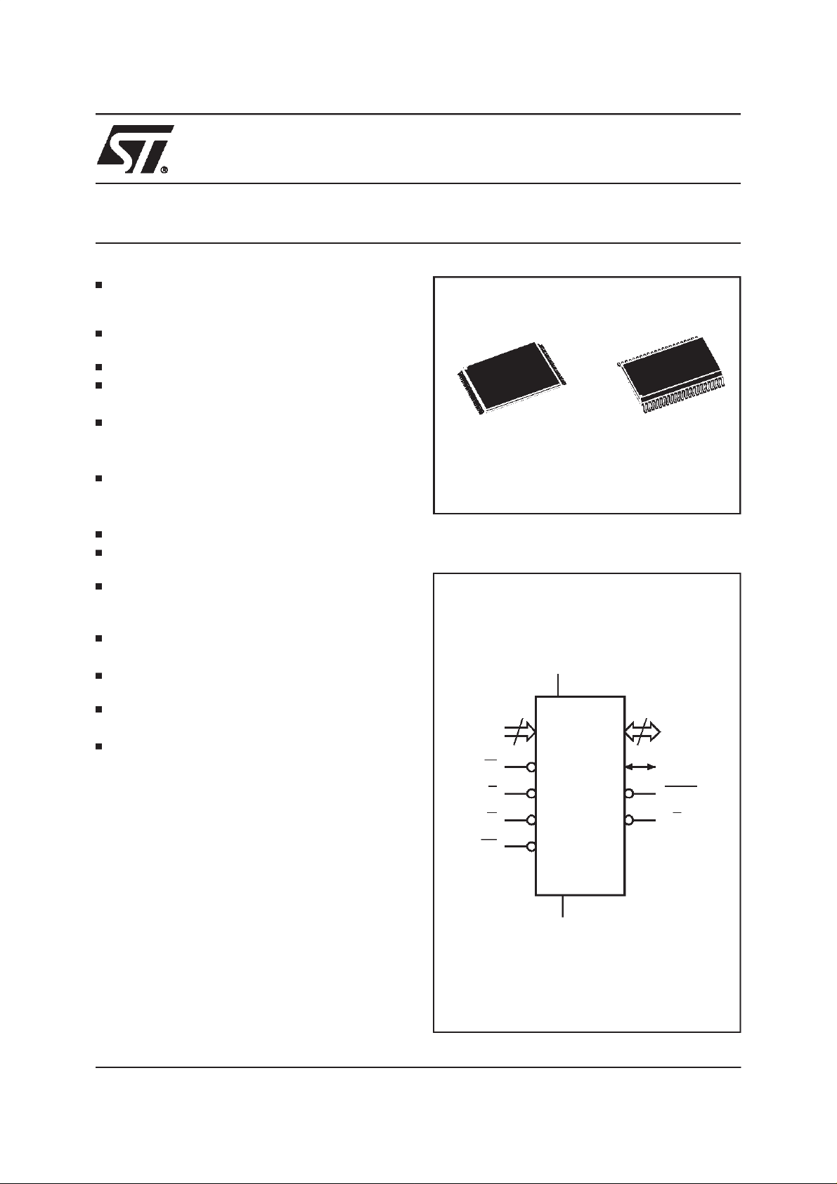
DESCRIPTION
The M29W800 is a non-volatilememory that may
beerasedelectricallyat theblock or chipleveland
programmedin-systemonaByte-by-Byteor Wordby-Wordbasisusingonly a single2.7V to 3.6V V
supply. For Program and Erase operations the
necessary high voltages are generated internally.
The device can also be programmed in standard
programmers.
Thearraymatrixorganisationallowseach block to
be erased and reprogrammed without affecting
otherblocks.Blockscan be protectedagainst programing and erase on programming equipment,
CC
12 x 20 mm
Figure1. LogicDiagram
V
CC
19
A0-A18
W
E
G
RP
M29W800T
M29W800B
V
SS
M29W800T
M29W800B
NOT FOR NEW DESIGN
44
1
SO44 (M)TSOP48 (N)
15
DQ0-DQ14
DQ15A–1
BYTE
RB
AI02178
June 1999 1/33
Thisis informationon a product stillin productionbutnotrecommended for newdesigns.
Page 2
M29W800T, M29W800B
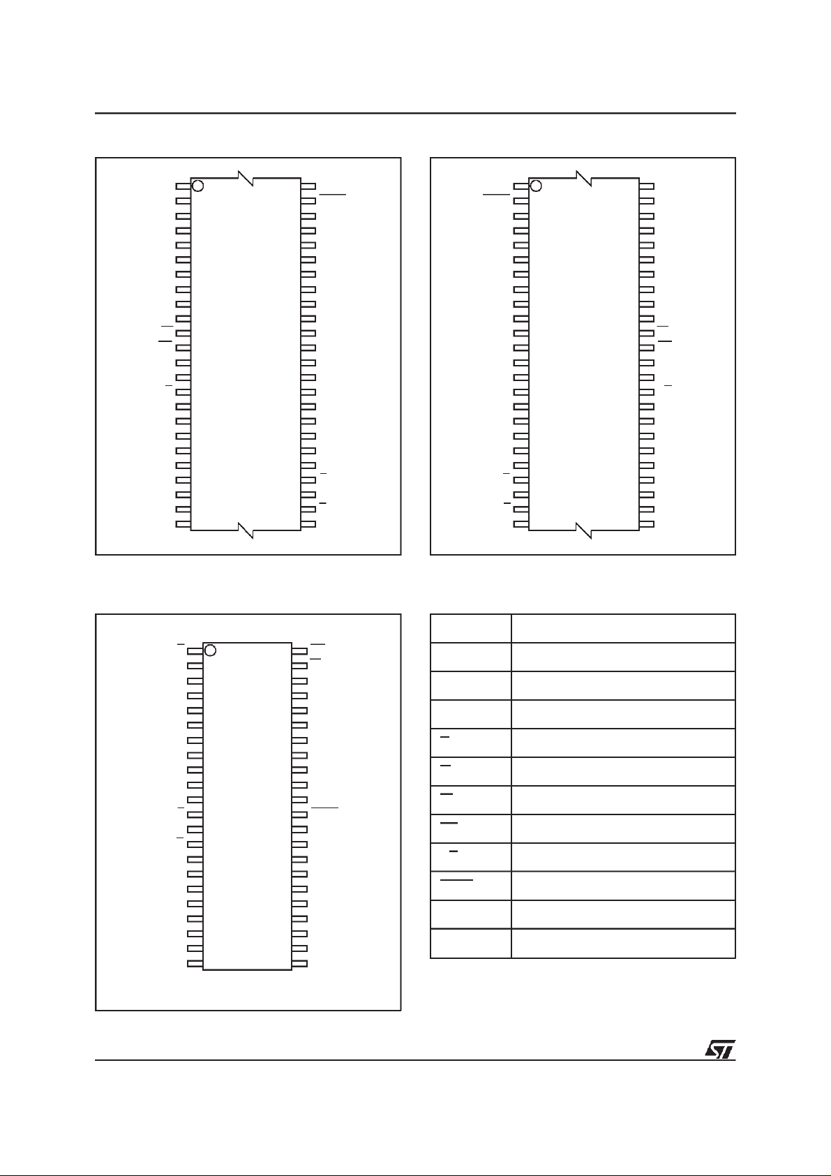
Figure2A. TSOPPin Connections
1
A15
A14
A13
A12
A11
A10 DQ14
A9
A8
NC
NC
W
RP
NC
NC
RB
A18
A17
A7
A6
A5
A4
A3
A2
A1
M29W800T
12
M29W800B
13
(Normal)
24 25
48
37
36
AI02179
A16
BYTE
V
SS
DQ15A–1
DQ7
DQ6
DQ13
DQ5
DQ12
DQ4
V
CC
DQ11
DQ3
DQ10
DQ2
DQ9
DQ1
DQ8
DQ0
G
V
SS
E
A0
Figure2B. TSOPReverse Pin Connections
A16
BYTE
V
SS
DQ15A–1
DQ7
DQ14
DQ6
DQ13
DQ5
DQ12
DQ4
V
CC
DQ11
DQ3
DQ10
DQ2
DQ9
DQ1
DQ8
DQ0
V
SS
A0
1
M29W800T
12
M29W800B
13
(Reverse)
G
E
24 25
AI02180
48
37
36
A15
A14
A13
A12
A11
A10
A9
A8
NC
NC
W
RP
NC
NC
RB
A18
A17
A7
A6
A5
A4
A3
A2
A1
Warning: NC = Not Connected. Warning: NC = Not Connected.
Figure2C. SO Pin Connections
Table 1. Signal Names
A0-A18 Address Inputs
RB
1
2
A18
3
A17 A8
A7
4
5
A6
6
A5
A4
7
A3
8
A2
9
A1
10
A0
11
M29W800T
M29W800B
12
13
14
15
16
17DQ1
18
19
20
21
AI02181
V
SS
DQ0
DQ8
DQ9
DQ10
DQ3
DQ11
E
G
44
43
42
41
40
39
38
37
36
35
34
33
32
31
30
29
28
27
26
25
24
2322
RP
W
A9
A10
A11
A12
A13
A14
A15
A16
BYTE
V
SS
DQ15A–1
DQ7
DQ14
DQ6
DQ13
DQ5DQ2
DQ12
DQ4
V
CC
DQ0-DQ7 Data Input/Outputs, Command Inputs
DQ8-DQ14 Data Input/Outputs
DQ15A–1 Data Input/Output or Address Input
E Chip Enable
G Output Enable
W Write Enable
RP Reset / Block TemporaryUnprotect
RB Ready/Busy Output
BYTE Byte/Word Organisation
V
CC
V
SS
Supply Voltage
Ground
2/33
Page 3

M29W800T, M29W800B
Table2. AbsoluteMaximumRatings
Symbol Parameter Value Unit
T
A
T
BIAS
T
STG
(2)
V
IO
V
CC
V
(A9, E, G, RP)
Notes: 1. Except for therating ”OperatingTemperature Range”, stresses above those listed in the Table ”AbsoluteMaximum Ratings”
may cause permanent damage to thedevice. These are stress ratings only and operation of the device at these or any other
conditions above those indicated in the Operatingsections of this specification is not implied.Exposure to Absolute Maximum
Rating conditions for extended periods may affect device reliability.Refer also tothe STMicroelectronics SURE Program and other
relevant quality documents.
2. Minimum Voltagemay undershootto –2V during transition and for less than 20ns.
3. Depends on range.
Ambient Operating Temperature
Temperature Under Bias –50 to 125
Storage Temperature –65 to 150
Input or Output Voltages –0.6to 5 V
Supply Voltage –0.6to 5 V
(2)
A9, E, G, RP Voltage –0.6to 13.5 V
DESCRIPTION(Cont’d)
and temporarily unprotected to make changes in
the application. Each block can be programmed
and erased over 100,000 cycles.
Instructionsfor Read/Reset, Auto Select for reading the Electronic Signature or Block Protection
status,Programming,BlockandChipErase,Erase
Suspend and Resume are written to the devicein
cyclesofcommandstoaCommandInterfaceusing
standardmicroprocessorwrite timings.
Thedevice is offered in TSOP48(12 x20mm)and
SO44packages.Both normal and reversepinouts
are available for the TSOP48package.
Organisation
TheM29W800is organisedas1 M x8 or512Kx16
bitsselectableby the BYTEsignal.WhenBYTE is
Low the Byte-wide x8 organisationis selectedand
the address lines are DQ15A–1and A0-A18. The
Data Input/Output signal DQ15A–1 acts as address line A–1 which selects the lower or upper
Byteof the memoryword for output on DQ0-DQ7,
DQ8-DQ14 remain at High impedance. When
BYTEis Highthe memoryuses the addressinputs
A0-A18 and the Data Input/Outputs DQ0-DQ15.
Memory control is provided by Chip Enable E,
OutputEnable G and WriteEnable W inputs.
AReset/BlockTemporaryUnprotection RPtri-level
input providesa hardware reset when pulled Low,
andwhen heldHigh(atV
)temporarily unprotects
ID
blocks previously protected allowing them to be
programedanderased.Erase andProgramoperations are controlled by an internal Program/Erase
Controller(P/E.C.). StatusRegisterdata output on
DQ7providesa DataPollingsignal,and DQ6 and
DQ2provideToggle signalstoindicatethe state of
(1)
(3)
–40 to 85
C
°
C
°
C
°
the P/E.C operations. A Ready/Busy RB output
indicatesthecompletionof theinternalalgorithms.
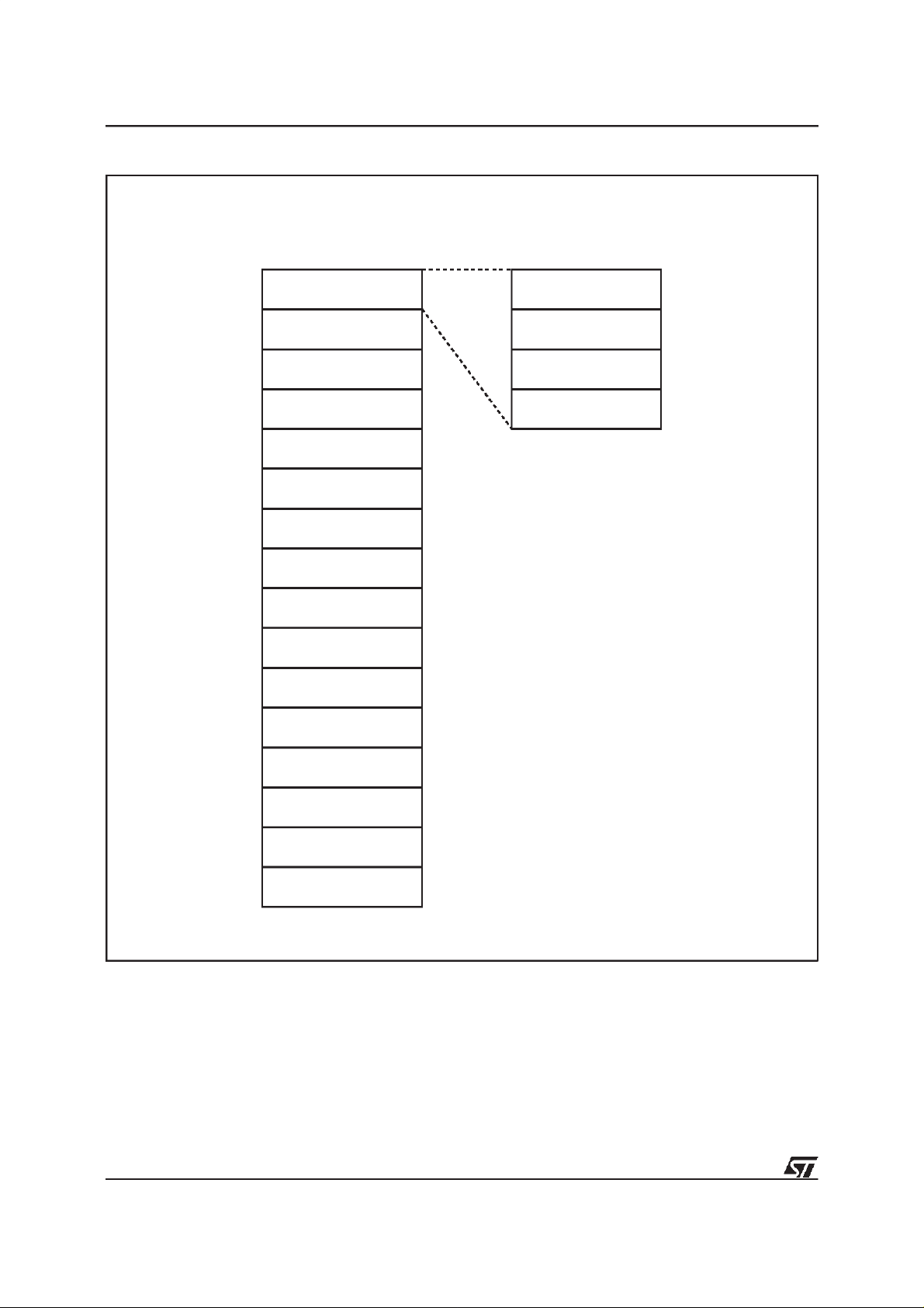
MemoryBlocks
Thedevicesfeatureasymmetrically blockedarchitectureprovidingsystem memory integration.Both
M29W800Tand M29W800Bdeviceshavean array
of 19 blocks, one Boot Block of 16 KBytes or 8
KWords, two Parameter Blocks of 8 KBytes or 4
KWords, one Main Block of 32 KBytes or 16
KWordsand fifteenMainBlocksof 64KBytesor 32
KWords.TheM29W800ThastheBoot Block atthe
top of the memory add ress space and the
M29W800Blocates the Boot Block starting at the
bottom. The memory maps are showed in Figure
3.
Each block can be erased separately, any combi-
nation of blocks can be specified for multi-block
eraseor the entirechip may beerased.TheErase
operations are managed automatically by the
P/E.C. The block erase operation can be suspended in order to read from or program to any
blocknot being ersased, and then resumed.
Block protection provides additionaldata security.
Each block can be separatelyprotected or unprotectedagainst Program or Erase on programming
equipment.All previously protected blocks can be
temporarilyunprotectedin the application.
Bus Operations
The following operations can be performed using
theappropriatebus cycles:Read(Array,Electronic
Signature, Block Protection Status), Write command, Output Disable,Standby,Reset, Block Protection, Unprotection, Protection Verify,
Unprotection Verifyand Block Temporary Unprotection.See Tables4 and5.
3/33
Page 4
M29W800T, M29W800B
Figure3A. TopBootBlock Memory Map and Block Address Table
TOP BOOT BLOCK
7FFFFh
78000h
77FFFh
70000h
6FFFFh
68000h
67FFFh
60000h
5FFFFh
58000h
57FFFh
50000h
4FFFFh
48000h
47FFFh
40000h
3FFFFh
38000h
37FFFh
30000h
2FFFFh
28000h
27FFFh
20000h
1FFFFh
18000h
17FFFh
10000h
0FFFFh
08000h
07FFFh
00000h
Byte-WideWord-Wide
FFFFFh
F0000h
EFFFFh
E0000h
DFFFFh
D0000h
CFFFFh
C0000h
BFFFFh
B0000h
AFFFFh
A0000h
9FFFFh
90000h
8FFFFh
80000h
7FFFFh
70000h
6FFFFh
60000h
5FFFFh
50000h
4FFFFh
40000h
3FFFFh
30000h
2FFFFh
20000h
1FFFFh
10000h
0FFFFh
00000h
64K MAIN BLOCK
64K MAIN BLOCK
64K MAIN BLOCK
64K MAIN BLOCK
64K MAIN BLOCK
64K MAIN BLOCK
64K MAIN BLOCK
64K MAIN BLOCK
64K MAIN BLOCK
64K MAIN BLOCK
64K MAIN BLOCK
64K MAIN BLOCK
64K MAIN BLOCK
64K MAIN BLOCK
64K MAIN BLOCK
16K BOOT BLOCK
8K PARAMETER BLOCK
8K PARAMETER BLOCK
32K MAIN BLOCK
AI01725B
Byte-Wide Word-Wide
FFFFFh
FC000h
FBFFFh
FA000h
F9FFFh
F8000h
F7FFFh
F0000h
7FFFFh
7E000h
7DFFFh
7D000h
7CFFFh
7C000h
7BFFFh
78000h
4/33
Page 5
Figure3B. Bottom BootBlock MemoryMap andBlock Address Table
BOTTOM BOOT BLOCK
Byte-WideWord-Wide
FFFFFh
78000h
77FFFh
70000h
6FFFFh
68000h
67FFFh
60000h
5FFFFh
58000h
57FFFh
50000h
4FFFFh
48000h
47FFFh
40000h
3FFFFh
38000h
37FFFh
30000h
2FFFFh
28000h
27FFFh
20000h
1FFFFh
18000h
17FFFh
10000h
0FFFFh
08000h
07FFFh
00000h
FFFFFh7FFFFh
F0000h
EFFFFh
E0000h
DFFFFh
D0000h
CFFFFh
C0000h
BFFFFh
B0000h
AFFFFh
A0000h
9FFFFh
90000h
8FFFFh
80000h
7FFFFh
70000h
6FFFFh
60000h
5FFFFh
50000h
4FFFFh
40000h
3FFFFh
30000h
2FFFFh
20000h
1FFFFh
10000h
0FFFFh
00000h
64K MAIN BLOCK
64K MAIN BLOCK
64K MAIN BLOCK
64K MAIN BLOCK
64K MAIN BLOCK
64K MAIN BLOCK
64K MAIN BLOCK
64K MAIN BLOCK
64K MAIN BLOCK
64K MAIN BLOCK
64K MAIN BLOCK
64K MAIN BLOCK
64K MAIN BLOCK
64K MAIN BLOCK
64K MAIN BLOCK
32K MAIN BLOCK
8K PARAMETER BLOCK
8K PARAMETER BLOCK
16K BOOT BLOCK
M29W800T, M29W800B
Byte-Wide Word-Wide
0FFFFh
08000h
07FFFh
06000h
05FFFh
04000h
03FFFh
00000h
07FFFh
04000h
03FFFh
03000h
02FFFh
02000h
01FFFh
00000h
AI01731B
5/33
Page 6
M29W800T, M29W800B
Table3A. M29W800TBlockAddress Table
Address Range (x8) Address Range (x16) A18 A17 A16 A15 A14 A13 A12
00000h-0FFFFh 00000h-07FFFh 0 0 0 0 X X X
10000h-1FFFFh 08000h-0FFFFh 0 0 0 1 X X X
20000h-2FFFFh 10000h-17FFFh 0 0 1 0 X X X
30000h-3FFFFh 18000h-1FFFFh 0 0 1 1 X X X
40000h-4FFFFh 20000h-27FFFh 0 1 0 0 X X X
50000h-5FFFFh 28000h-2FFFFh 0 1 0 1 X X X
60000h-6FFFFh 30000h-37FFFh 0 1 1 0 X X X
70000h-7FFFFh 38000h-3FFFFh 0 1 1 1 X X X
80000h-8FFFFh 40000h-47FFFh 1 0 0 0 X X X
90000h-9FFFFh 48000h-4FFFFh 1 0 0 1 X X X
A0000h-AFFFFh 50000h-57FFFh 1 0 1 0 X X X
B0000h-BFFFFh 58000h-5FFFFh 1 1 1 1 X X X
C0000h-CFFFFh 60000h-67FFFh 1 1 0 0 X X X
D0000h-DFFFFh 68000h-6FFFFh 1 1 0 1 X X X
E0000h-EFFFFh 70000h-77FFFh 1 1 1 0 X X X
F0000h-F7FFFh 78000h-7BFFFh 1 1 1 1 0 X X
F8000h-F9FFFh 7C000h-7CFFFh 1 1 1 1 1 0 0
FA000h-FBFFFh 7D000h-7DFFFh 1 1 1 1 1 0 1
FC000h-FFFFFh 7E000h-7FFFFh 1 1 1 1 1 1 X
CommandInterface
Instructions,made up of commands written in cycles,canbe givento theProgram/EraseController
through a Command Interface (C.I.). For added
dataprotection,programor eraseexecutionstarts
after4 or6cycles.The first,second,fourthandfifth
This Coded sequence is the same for all Program/Erase Controller instructions. The ’Command’itself and its confirmation,when applicable,
are given on the third, fourth or sixth cycles. Any
incorrectcommandor any impropercommandsequence will resetthe device to Read Array mode.
cycles are used to input Coded cycles to the C.I.
6/33
Page 7
M29W800T, M29W800B
Table3B. M29W800BBlock Address Table
Address Range (x8) Address Range (x16) A18 A17 A16 A15 A14 A13 A12
00000h-03FFFh 00000h-01FFFh 0 0 0 0 0 0 X
04000h-05FFFh 02000h-02FFFh 0 0 0 0 0 1 0
06000h-07FFFh 03000h-03FFFh 0 0 0 0 0 1 1
08000h-0FFFFh 04000h-07FFFh 0 0 0 0 1 X X
10000h-1FFFFh 08000h-0FFFFh 0 0 0 1 X X X
20000h-2FFFFh 10000h-17FFFh 0 0 1 0 X X X
30000h-3FFFFh 18000h-1FFFFh 0 0 1 1 X X X
40000h-4FFFFh 20000h-27FFFh 0 1 0 0 X X X
50000h-5FFFFh 28000h-2FFFFh 0 1 0 1 X X X
60000h-6FFFFh 30000h-37FFFh 0 1 1 0 X X X
70000h-7FFFFh 38000h-3FFFFh 0 1 1 1 X X X
80000h-8FFFFh 40000h-47FFFh 1 0 0 0 X X X
90000h-9FFFFh 48000h-4FFFFh 1 0 0 1 X X X
A0000h-AFFFFh 50000h-57FFFh 1 0 1 0 X X X
B0000h-BFFFFh 58000h-5FFFFh 1 0 1 1 X X X
C0000h-CFFFFh 60000h-67FFFh 1 1 0 0 X X X
D0000h-DFFFFh 68000h-6FFFFh 1 1 0 1 X X X
E0000h-EFFFFh 70000h-77FFFh 1 1 1 0 X X X
F0000h-FfFFFh 78000h-7FFFFh 1 1 1 1 X X X
Instructions
Seven instructions are defined to perform Read
Array,AutoSelect(toreadthe ElectronicSignature
or BlockProtectionStatus),Program,BlockErase,
Chip Erase, Erase Suspend and Erase Resume.
The internal P/E.C. automatically handlesall timing and verification of the Program and Erase
operations.TheStatus Register Data Polling,Toggle, Error bits and the RB output may be read at
anytime, during programmingor erase, to monitor
the progress of theoperation.
Instructionsarecomposedof upto six cycles. The
first two cycles input a Coded sequence to the
CommandInterfacewhich iscommon toall instructions(see Table 8).
The third cycle inputs the instruction set-up com-
data, Electronic Signature or Block Protection
Status for Read operations.In order to give additional data protection,the instructionsforProgram
and Block or Chip Erase require further command
inputs. For a Programinstruction,the fourth command cycle inputs the address and data to be
programmed. For an Erase instruction (Block or
Chip), the fourth and fifth cycles input a further
Coded sequence before the Erase confirm commandonthesixthcycle.Erasureofamemoryblock
may be suspended, in order to read data from
anotherblock or to program data inanotherblock,
and then resumed.
When power is first applied or if V
, the command interface is reset to Read
V
LKO
CC
Array.
mand. Subsequent cycles output the addressed
falls below
7/33
Page 8

M29W800T, M29W800B
SIGNALDESCRIPTIONS
See Figure 1 and Table1.
AddressInputs(A0-A18). The addressinputsfor
thememoryarray are latchedduringawriteoperation on the falling edge at Chip Enable E or Write
EnableW. In Word-wide organisation the address
lines are A0-A18, in Byte-wide organisation
DQ15A–1acts as an additional LSB address line.
WhenA9 israised to V
, eithera Read Electronic
ID
Signature Manufacturer or Device Code, Block
Protection Status or a Write Block Protection or
Block Unprotection is enabled depending on the
combinationof levelson A0,A1, A12andA15.
Data Input/Outputs (DQ0-DQ7). These Inputs/Outputsare used in the Byte-wideand Wordwide organisations. The inpu t is data to be
programmed in the memory array or a command
to be written to the C.I. Both are latched on the
rising edge of Chip Enable E or Write Enable W.
The output is data from the Memory Array, the
Electronic Signature Manufacturer or Device
codes, the Block Protection Status or the Status
registerData Polling bit DQ7, the ToggleBits DQ6
and DQ2, the Error bit DQ5 or the EraseTimer bit
DQ3. Outputs are valid when Chip Enable E and
Output Enable G are active. The output is high
impedance when the chip is deselected or the
outputsaredisabledandwhenRPis ataLowlevel.
Data Input/Outputs (DQ8-DQ14and DQ15A–1).
These Inputs/Outputsare additionally used in the
Word-wide organisation.WhenBYTEisHighDQ8DQ14 and DQ15A–1 act as the MSB of the Data
Inputor Output,functioningas described for DQ0DQ7 above, and DQ8 - DQ15 are ’don’t care’ for
commandinputs or statusoutputs. When BYTEis
Low,DQ0-DQ14arehighimpedance,DQ15A–1is
theAddressA–1input.
Chip Enable (E). The Chip Enable inputactivates
the memory control logic, input buffers, decoders
andsenseamplifiers.E Highdeselectsthememory
andreducesthe powerconsumptiontothestandby
level. E can also be used to control writing to the
commandregister and to the memory array, while
Wremainsata lowlevel.TheChipEnablemust be
forcedto V
duringthe BlockUnprotectionopera-
ID
tion.
Output Enable (G). The Output Enable gates the
outputs through the data buffers during a read
operation. When G is High the outputs are High
impedance. G must be forced to V
level during
ID
BlockProtectionand Unprotection operations.
WriteEnable(W).Thisinputcontrolswritingto the
CommandRegisterand Addressand Datalatches.
Byte/Word Organization Select (BYTE). The
BYTEinputselectstheoutputconfigurationfor the
device: Byte-wide (x8) mode or Word-wide (x16)
mode. When BYTEis Low,the Byte-widemode is
selectedand thedata isread and programmedon
DQ0-DQ7. In this mode, DQ8-DQ14 are at high
impedance and DQ15A–1 is the LSB address.
When BYTE is High, the Word-wide mode is selected and the data is read and programmed on
DQ0-DQ15.
Ready/Busy Output (RB). Ready/Busy is an
open-drainoutputandgivestheinternalstateofthe
P/E.C. of the device. When RB is Low, the device
is Busy with a Program or Erase operation and it
will not accept any additional program or erase
instructionsexcept theEraseSuspendinstruction.
WhenRB is High, thedeviceis readyforany Read,
Program or Erase operation. The RB will also be
Highwhen the memoryis put inEraseSuspendor
Standbymodes.
Reset/Block Temporary Unprotect Input (RP).
The RP Input provides hardware reset and protected block(s) temporary unprotection functions.
Resetof the memory is acheivedby pulling RP to
foratleastt
V
IL
. Whentheresetpulseisgiven,
PLPX
if the memoryis in Reador Standby modes, it will
be available for new operations in t
PHEL
after the
risingedgeofRP.If thememoryis in Erase,Erase
Suspend or Program modes the reset will take
duringwhichtheRBsignalwillbe held at VIL.
t
PLYH
The end of the memory reset will be indicated by
the rising edge of RB. A hardware reset during an
Erase or Program operation will corrupt the data
being programmed or the sector(s) being erased.
SeeTable 14 and Figure 9.
Temporary block unprotectionis made by holding
RP at V
. In this condition previously protected
ID
blockscan be programmed or erased.The transitionof RPfrom V
to VIDmustslowerthant
IH
PHPHH
See Table 15 and Figure 9. When RP is returned
from V
to VIHall blocks temporarily unprotected
ID
will be again protected.
V
Supply Voltage. The power supply for all
CC
operations(Read,Programand Erase).
Ground. VSSis the reference for all voltage
V
SS
measurements.
.
8/33
Page 9

M29W800T, M29W800B
DEVICEOPERATIONS
See Tables 4, 5 and 6.
Read. Read operations are used to output the
contents of the Memory Array,the ElectronicSignature,theStatusRegisteror the BlockProtection
Status.Both Chip Enable E and Output Enable G
must be low in order to read the output of the
memory.
Write.WriteoperationsareusedtogiveInstruction
Commandstothe memory or to latch input data to
beprogrammed.Awrite operationis initiatedwhen
Chip Enable E isLow and Write Enable W is Low
withOutputEnableG High.Addressesarelatched
onthefallingedge of W or E whicheveroccurslast.
CommandsandInputDataarelatchedontherising
edgeof W or E whicheveroccursfirst.
OutputDisable. The data outputsarehighimpedancewhen the OutputEnable G is High with Write
EnableW High.
Standby. The memory is in standby when Chip
EnableE is Highand theP/E.C.is idle.The power
consumption is reduced to the standby level and
the outputs are high impedance, independent of
the Output Enable G or WriteEnable W inputs.
AutomaticStandby. After 150ns of bus inactivity
andwhen CMOS levels are drivingthe addresses,
the chip automatically enters a pseudo-standby
modewhereconsumptionis reducedto theCMOS
standbyvalue,while outputsstill drivethe bus.
ElectronicSignature. Two codes identifying the
manufacturer and thedevicecanbe read fromthe
memory. The manufacturer’s code for STMicroelectronicsis20h,thedevicecodeisD7hforthe
M29W800T(TopBoot)and 5BhfortheM29W800B
(Bottom Boot). These codes allow programming
equipment or applications to automatically match
their interface to the characteristics of the
M29W800.The ElectronicSignatureis outputby a
Read operationwhen the voltage applied to A9 is
andaddressinputsA1 isLow.The manufac-
atV
ID
turer code is output when the Address input A0 is
Low and the device code when this input is High.
Other Address inputs are ignored. The codes are
output on DQ0-DQ7.
TheElectronicSignaturecan alsobe read,without
raisingA9 to V
, bygiving the memorythe Instruc-
ID
tion AS. If the Byte-wide configuration is selected
thecodes areoutputonDQ0-DQ7with DQ8-DQ14
atHigh impedance;if the Word-wideconfiguration
isselectedthe codes are output on DQ0-DQ7with
DQ8-DQ15at 00h.
Block Protection. Each block can be separately
protected against Program or Erase on programming equipment. Block protection provides additional data security, as it disables all program or
eraseoperations.Thismodeisactivatedwhenboth
A9 and G are raised to V
and an address in the
ID
block is applied on A12-A18. Block protection is
initiatedon the edge of W falling to V
a delayof 100µs,the edge of W rising to V
. Then after
IL
IH
ends
theprotectionoperations.Blockprotectionverifyis
achievedby bringingG, E, A0and A6toV
, while W is atVIHandA9at VID. Underthese
toV
IH
andA1
IL
conditions,reading the data outputwill yield 01h if
the block defined by the inputs on A12-A18 is
protected.Any attempt to program or erasea protectedblockwill be ignoredby the device.
Block Temporary Unprotection. Any previously
protectedblock can be temporarilyunprotectedin
ordertochangestoreddata.Thetemporaryunprotection mode is activated by bringing RP to V
ID
During the temporary unprotection mode the previously protected blocks are unprotected. A block
can be selected and data can be modified by
executingtheEraseorPrograminstructionwiththe
RPsignalheldat V
. When RP is returnedto VIH,
ID
all the previously protected blocks are again protected.
Block Unprotection. All protected blocks can be
unprotected on programming equipment to allow
updating of bit contents. All blocks must first be
protectedbefore theunprotectionoperation.Block
unprotectionis activatedwhen A9, G and E are at
and A12, A15 at VIH. Unprotection is initiated
V
ID
bytheedgeofWfallingto V
. Afteradelayof10ms,
IL
the unprotection operation will end. Unprotection
verify is achievedby bringing G and E to V
A0 is at V
atV
ID
, A6 and A1 are at VIHand A9 remains
IL
. Inthese conditions,readingtheoutput data
IL
while
will yield 00h if the block defined by the inputs
A12-A18has been succesfully unprotected. Each
block must be separatelyverified by giving its address in order to ensure that it has been unprotected.
.
9/33
Page 10
M29W800T, M29W800B
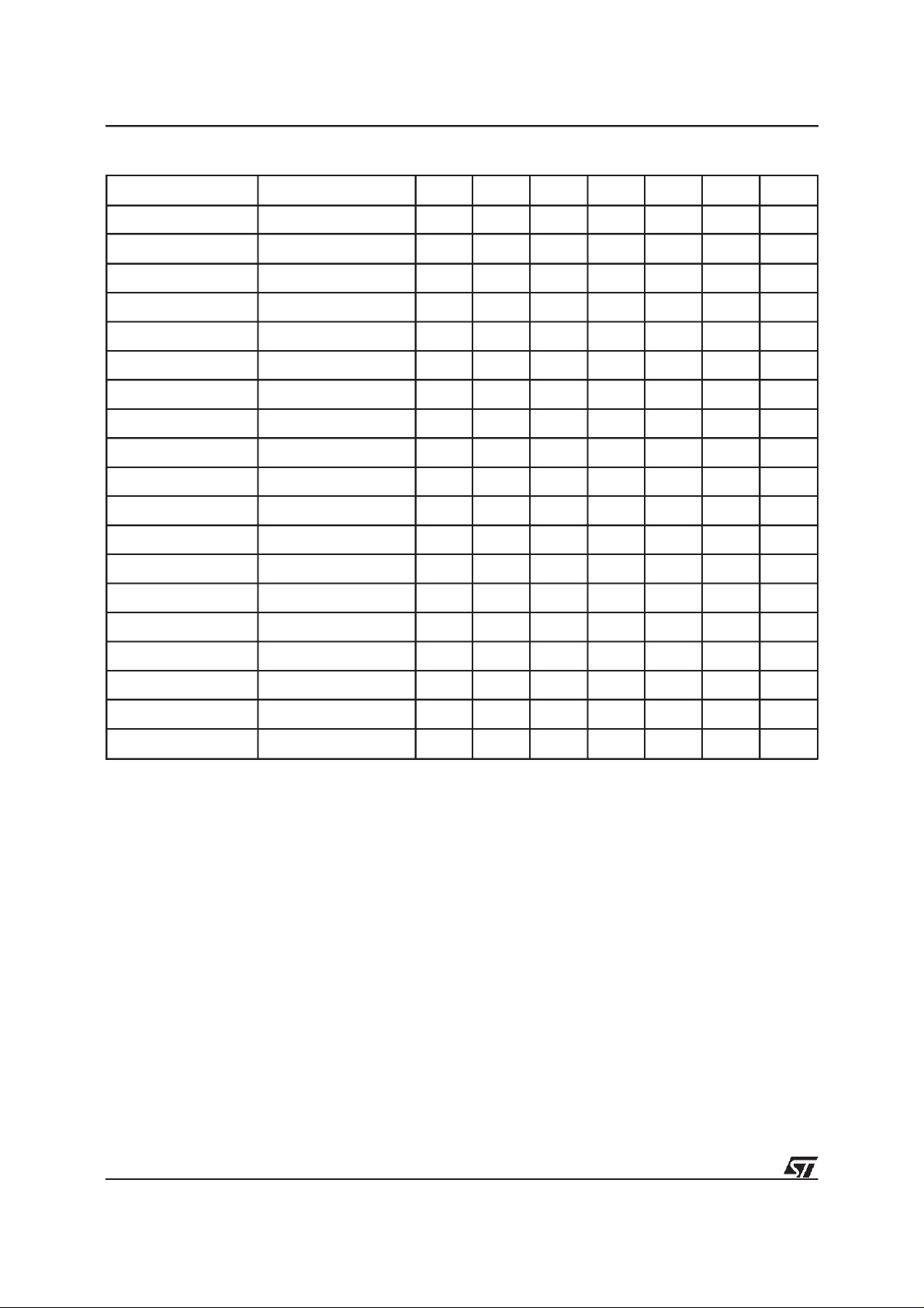
Table4. User Bus Operations
(1)
Operation E G W RP BYTE A0 A1 A6 A9 A12 A15
Read Word V
Read Byte V
Write Word V
Write Byte V
Output Disable V
Standby V
ILVIL
ILVIL
ILVIH
ILVIH
ILVIH
IH
Reset X X X V
Block
Protection
Blocks
Unprotection
Block
Protection
Verify
Block
Unprotection
Verify
Block
Temporary
Unprotection
Notes: 1. X = V
(2,4) V
(2,4)
(2,4)
ILVIDVIL
(4)VIDVIDVIL
VILV
VILV
XX X V
or V
IL
2. Block Address must be given on A12-A18bits.
3. See Table6.
4. Operation performed onprogramming equipment.
IH
V
V
V
IH
IH
V
V
IH
IH
V
V
IL
IH
V
V
IL
IH
V
V
IH
IH
A0 A1 A6 A9 A12 A15
IH
V
A0 A1 A6 A9 A12 A15
IL
V
A0 A1 A6 A9 A12 A15 Data Input Data Input
IH
V
A0 A1 A6 A9 A12 A15
IL
X X X X X X X Hi-Z Hi-Z Hi-Z
XXVIHX X X X X X X Hi-Z Hi-Z Hi-Z
X X X X X X X Hi-Z Hi-Z Hi-Z
IL
Pulse V
Pulse V
V
IL
IH
V
IL
IH
XXXXVIDXX X X X
IH
XXXXVIDVIHV
IH
V
XVILVIHVILVIDA12 A15 X X
IH
V
XVILVIHVIHVIDA12 A15 X X
IH
X XXXXXX X X X
ID
DQ15
A–1
Data
Output
Address
Input
Address
Input
XXX
IH
DQ8-
DQ14
Data
Output
Hi-Z
Hi-Z
DQ0-DQ7
Data
Output
Data
Output
Data
Input
Data
Input
Block
Protect
Status
Block
Protect
Status
(3)
(3)
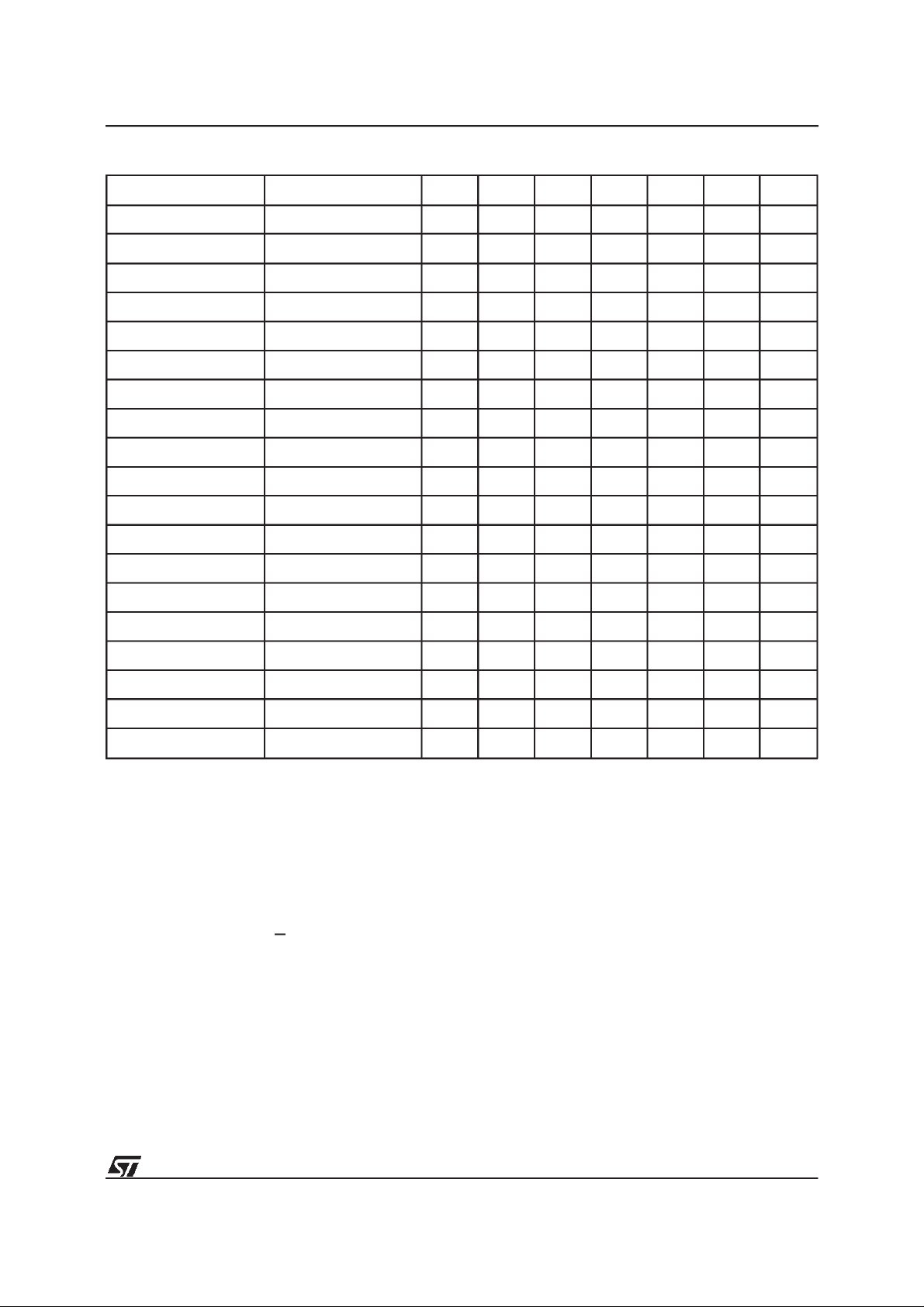
Table5. Read Electronic Signature(followingAS instructionor with A9 = VID)
Org. Code Device E G W BYTE A0 A1
Word-
wide
Manufact.
Code
Device
Code
Manufact.
Code
M29W800T V
M29W800B V
V
VILV
IL
VILV
IL
VILV
IL
V
VILV
IL
V
IH
V
IH
V
IH
V
IH
VILVILDon’t Care 0 00h 20h
IH
V
IH
IH
IL
IHVIL
V
IHVIL
VILVILDon’t Care
Byte-
wide
Device
M29W800T V
IL
VILV
V
IH
V
IL
IHVIL
Code
M29W800B V
IL
VILV
V
IH
V
IL
IHVIL
Other
Addresses
Don’t Care 0 00h D7h
Don’t Care 0 00h 5Bh
Don’t Care
Don’t Care
DQ15
A–1
Don’t
Care
Don’t
Care
Don’t
Care
Table6. Read Block Protectionwith AS Instruction
Code E G W A0 A1 A12-A18
Protected Block V
Unprotected Block V
IL
IL
V
IL
V
IL
V
IH
V
IH
V
IL
V
IL
V
IH
V
IH
Block Address Don’t Care 01h
Block Address Don’t Care 00h
Addresses
Other
DQ8-
DQ14
DQ0-
DQ7
Hi-Z 20h
Hi-Z D7h
Hi-Z 5Bh
DQ0-DQ7
10/33
Page 11

M29W800T, M29W800B
INSTRUCTIONS AND COMMANDS
The Command Interface latches commands written to the memory.Instructionsare made up from
one or morecommands to perform Read Memory
Array, ReadElectronicSignature,Read BlockProtection, Program, Block Erase, Chip Erase, Erase
Suspend and Erase Resume. Commands are
made of address and data sequences. The instructionsrequirefrom1 to6 cycles,thefirstorfirst
threeof whichare always write operationsused to
initiatethe instruction.They are followed by either
furtherwrite cyclesto confirmthe first commandor
executethe commandimmediately.Commandsequencing must be followed exactly. Any invalid
combinationof commands will reset the device to
Read Array. The increased number of cycles has
been chosen to assure maximum data security.
Instructionsare initialised by two initial Coded cycleswhichunlockthe CommandInterface.In addition, for Erase, instruction confirmation is again
precededby thetwo Coded cycles.
StatusRegister Bits
P/E.C.statusis indicatedduring executionby Data
Polling on DQ7, detectionof Toggle on DQ6 and
DQ2, or Erroron DQ5 and EraseTimer DQ3 bits.
Any read attempt during Program or Erase commandexecutionwillautomaticallyoutputthesefive
StatusRegisterbits. TheP/E.C.automaticallysets
bits DQ2, DQ3, DQ5, DQ6 and DQ7. Other bits
(DQ0, DQ1 and DQ4) are reserved for future use
and should be masked. See Tables9 and 10.
Data Polling Bit (DQ7). WhenProgramming operations are in progress, this bit outputs the complement of the bit being programmed on DQ7.
DuringEraseoperation,it outputsa ’0’.After completionof the operation, DQ7 will outputthe bit last
programmed or a ’1’ after erasing. Data Polling is
valid and only effective during P/E.C. operation,
that is after the fourth W pulse forprogrammingor
after the sixth W pulse for erase. It must be performedat the address beingprogrammedor at an
address within the block being erased. If all the
blocksselectedfor erasureareprotected,DQ7 will
beset to ’0’forabout100µs,and then return to the
previous addressed memorydata value.See Figure11for the DataPolling flowchart and Figure 10
for the Data Polling waveforms. DQ7 will also flag
the Erase Suspend mode by switching from ’0’to
’1’ at the start of the Erase Suspend. In order to
monitor DQ7 in the Erase Suspend mode an address within a block being erased must be provided. For a Read Operation in Erase Suspend
mode, DQ7 will output ’1’ if the read is attempted
ona blockbeingerasedand thedatavalueonother
blocks. During Program operation in Erase SuspendMode, DQ7 will have the same behaviouras
in the normal program execution outside of the
suspendmode.
ToggleBit (DQ6). When Programmingor Erasing
operationsare in progress,successiveattemptsto
readDQ6willoutputcomplementarydata.DQ6 will
toggle following toggling of either G, or E when G
is low. The operation is completed when two successivereads yieldthesameoutputdata. Thenext
readwilloutputthe bitlastprogrammedor a’1’after
erasing. The toggle bit DQ6 is valid only during
P/E.C. operations,that is after the fourth W pulse
for programming or after the sixth W pulse for
Erase. If the blocks selected for erasure are protected, DQ6 will toggle for about 100µs and then
returnback toRead.DQ6willbe setto ’1’if a Read
operationisattemptedon anEraseSuspendblock.
When erase is suspendedDQ6 will toggle during
programmingoperations in a block different to the
blockin Erase Suspend. Either E or Gtogglingwill
causeDQ6 to toggle.See Figure 12 for ToggleBit
flowchartandFigure 13 for ToggleBit waveforms.
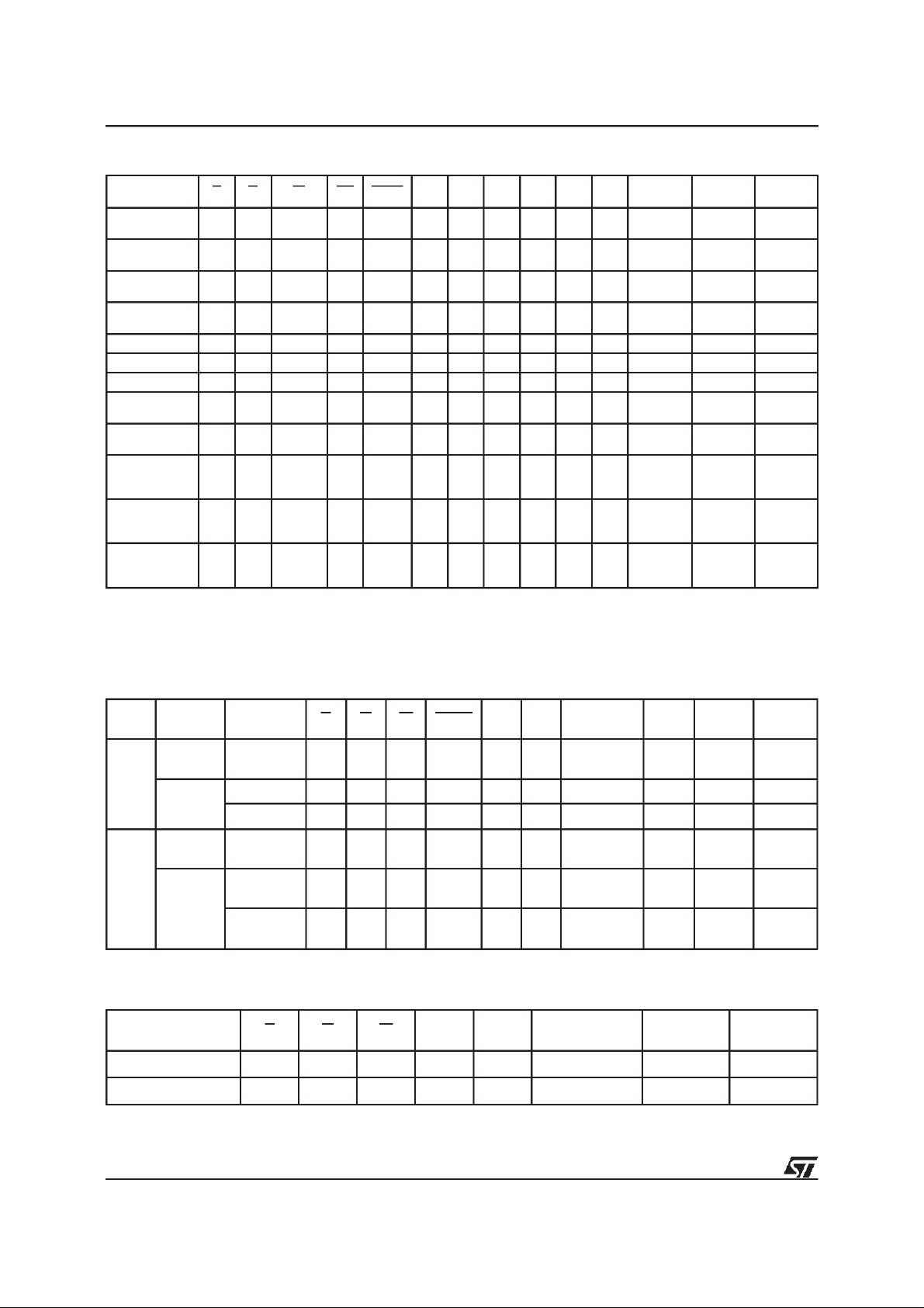
Table7. Commands
Hex Code Command
00h Invalid/Reserved
10h Chip Erase Confirm
20h Reserved
30h Block Erase Resume/Confirm
80h Set-up Erase
90h
A0h Program
B0h Erase Suspend
F0h ReadArray/Reset
Read Electronic Signature/
Block Protection Status
11/33
Page 12

M29W800T, M29W800B
Table8. Instructions
(1)
Mne. Instr. Cyc. 1st Cyc. 2nd Cyc. 3rd Cyc. 4th Cyc. 5th Cyc. 6th Cyc. 7th Cyc.
RD
(2,4)
Read/Reset
MemoryArray
(3,7)
Addr.
1+
Data F0h
Byte AAAAh 5555h AAAAh
(3,7)
Addr.
3+
Word 5555h 2AAAh 5555h
X
Read Memory Array until a new write cycle is initiated.
ReadMemory Array untila new write cycle
isinitiated.
Data AAh 55h F0h
(4)
AutoSelect 3+
AS
Addr.
(3,7)
Word 5555h 2AAAh 5555h
ReadElectronic Signature or Block
Protection Status untila new write cycle is
initiated. SeeNote 5 and 6.
Byte AAAAh 5555h AAAAh
Data AAh 55h 90h
PG Program 4
BE Block Erase 6
Byte AAAAh 5555h AAAAh
(3,7)
Addr.
Word 5555h 2AAAh 5555h
Data AAh 55h A0h
Byte AAAAh 5555h AAAAh AAAAh 5555h
(3,7)
Addr.
Word 5555h 2AAAh 5555h 5555h 2AAAh
Program
Address
Program
Data
Read Data Polling or Toggle Bit
until Program completes.
Block
Address
Additional
Block
Data AAh 55h 80h AAh 55h 30h 30h
CE ChipErase 6
Addr.
Word 5555h 2AAAh 5555h 5555h 2AAAh 5555h
Byte AAAAh 5555h AAAAh AAAAh 5555h AAAAh
(3,7)
Data AAh 55h 80h AAh 55h 10h
(3,7)
ES
Notes: 1. Commands not interpreted in this table will default to read array mode.
Suspend
Erase
ER
Resume
2. A wait of t
before starting any new operation (see Table14 and Figure 9).
3. X = Don’t Care.
4. The first cycles of the RD or AS instructions are followed by read operations.Any number of read cycles can occur after
the command cycles.
5. Signature Address bits A0, A1, atV
Device code.
6. Block ProtectionAddress: A0, at V
7. For Coded cycles address inputs A15-A18are don’t care.
8. Optional, additional Blocks addresses must be entered within the erase timeout delay after last write entry,timeout status
can be verified through DQ3 value (see Erase TimerBit DQ3 description). When full command is entered,read Data Polling
or Togglebit until Erase is completed or suspended.
9. Read DataPolling, Toggle bits or RB until Erase completes.
10.During Erase Suspend, Read and Data Programfunctions are allowed in blocks not being erased.
isnecessary after a Read/Reset command if the memory was in an Erase or Program mode
PLYH
Erase
(10)
Addr.
1
Data B0h
(3,7)
Addr.
1
Data 30h
will outputManufacturercode (20h). Address bits A0 at VIHand A1, at VILwill output
IL
,A1atVIHand A15-A18 within the Block will output the Block Protectionstatus.
IL
X
Read until Togglestops, then read all the data needed from any
Block(s) not being erased then Resume Erase.
X
Read Data Polling or ToggleBits until Erase completes or Erase is
suspended another time
(8)
Note 9
12/33
Page 13

M29W800T, M29W800B
Table 9. Status Register Bits
DQ Name Logic Level Definition Note
’1’
Data
7
Polling
’0’ Erase On-going
DQ
DQ Program On-going
Erase Complete or erase
block in Erase Suspend
Program Complete or data
of non erase block during
Erase Suspend
Indicates the P/E.C. status, check during
Program or Erase, and on completion
before checking bits DQ5 for Program or
Erase Success.
6 ToggleBit
5 Error Bit
4 Reserved
Erase
3
Time Bit
2 ToggleBit
’-1-0-1-0-1-0-1-’ Erase or Program On-going Successive reads output complementary
DQ Program Complete
’-1-1-1-1-1-1-1-’
’1’ Program or Erase Error
’0’ Program or Erase On-going
’1’ Erase Timeout Period Expired
’0’
’-1-0-1-0-1-0-1-’
1
DQ
Erase Complete or Erase
Suspend on currently
addressed block
Erase TimeoutPeriod
On-going
Chip Erase, Erase or Erase
Suspend on the currently
addressed block.
Erase Error due to the
currently addressed block
(when DQ5 = ’1’).
Program on-going, Erase
on-going on another block or
Erase Complete
Erase Suspend read on
non Erase Suspend block
data on DQ6 while Programming or Erase
operations are on-going. DQ6 remains at
constant level when P/E.C. operations are
completed or Erase Suspend is
acknowledged.
This bit is set to ’1’in the case of
Programming or Erase failure.
P/E.C. Erase operation has started. Only
possible command entry is Erase Suspend
(ES).
An additionalblock to be erased in parallel
can be entered to the P/E.C.
Indicates the erase status and allows to
identify the erased block
1 Reserved
0 Reserved
Notes: Logic level ’1’is High, ’0’ is Low. -0-1-0-0-0-1-1-1-0- represent bit value in successive Read operations.
13/33
Page 14

M29W800T, M29W800B
Table10. Pollingand Toggle Bits
Mode DQ7 DQ6 DQ2
Program DQ7 Toggle 1
Erase 0 Toggle Note 1
Erase Suspend Read
(in EraseSuspend
block)
Erase Suspend Read
(outside Erase Suspend
block)
Erase Suspend Program DQ7 Toggle N/A
Note: 1. Toggleif the address is within a block being erased.
’1’ if the address is within a block not beingerased.
1 1 Toggle
DQ7 DQ6 DQ2
Toggle Bit (DQ2). This toggle bit, together with
DQ6, can be used to determinethe device status
duringthe Erase operations.It canalsobe usedto
identify the block being erased. During Erase or
Erase Suspend a read from a block being erased
will cause DQ2 to toggle. A read from a block not
being erased will set DQ2 to ’1’during erase and
to DQ2 during EraseSuspend.During Chip Erase
a read operation will cause DQ2 to toggle as all
blocks are being erased. DQ2 will be set to ’1’
duringprogramoperationand whenerase is complete. After erase completion and if the error bit
DQ5 is set to ’1’, DQ2 will toggle if the faultyblock
is addressed.
ErrorBit (DQ5). This bit is set to ’1’ by the P/E.C.
when there is a failure of programming, block
erase, or chiperase that results in invaliddata in
thememoryblock.In caseof anerrorinblockerase
or program,theblockin whichtheerror occuredor
to which the programmed data belongs, must be
discarded. The DQ5 failure condition will also appearifausertriesto programa’1’to a locationthat
ispreviouslyprogrammedto ’0’. Other Blocksmay
stillbe used.Theerrorbitresetsaftera Read/Reset
(RD)instruction.In caseof successof Programor
Erase,the errorbit will be set to ’0’.
Erase Timer Bit (DQ3). This bit is setto ’0’ by the
P/E.C. when the last block Erase command has
been entered to the Command Interface and it is
awaiting the Erase start. When the erase timeout
periodis finished,after 50µsto90µs, DQ3returns
to ’1’.
Coded Cycles
Thetwo Coded cyclesunlockthe CommandInterface.They are followedby aninput commandor a
confirmationcommand.The Codedcyclesconsist
of writing the data AAh at address AAAAh in the
Byte-wide configuration and at address 5555h in
the Word-wide configuration during the first cycle.
During the second cycle the Coded cyclesconsist
of writing the data 55h at address 5555h in the
Byte-wideconfiguration and at address 2AAAh in
theWord-wideconfiguration.IntheByte-wideconfigurationthe addresslines A–1toA14arevalid,in
Word-wideA0 to A15arevalid,otheraddresslines
are ’don’tcare’. The Coded cycleshappen on first
and second cycles of the commandwriteor on the
fourthand fifth cycles.
Instructions
See Table8.
Read/Reset (RD) Instruction. The Read/Reset
instruction consists of one write cycle giving the
commandF0h.Itcanbe optionallyprecededby the
twoCodedcycles.Subsequentread operationswill
read the memory array addressed and output the
data read. A wait state of 10µs isnecessaryafter
Read/Reset prior to any valid read if the memory
was in an Erase mode when the RD instruction is
given.
Auto Select (AS) Instruction. This instruction
uses the two Coded cycles followed by one write
cycle giving the command 90h to addressAAAAh
in the Byte-wideconfigurationor address5555hin
the Word-wide configuration for command set-up.
A subsequent read will output the manufacturer
code and the device code or the block protection
status dependingon the levels of A0 and A1. The
manufacturer code, 20h, is output when the addresseslinesA0 and A1 areLow,thedevicecode,
EEh for Top Boot, EFh for Bottom Boot is output
when A0 is Highwith A1 Low.
The AS instruction also allows access to the block
protectionstatus.AftergivingtheASinstruction,A0
is set to V
with A1 at VIH, while A12-A18 define
IL
the address of the block to be verified. A read in
these conditions will output a 01h if the block is
protectedand a 00h if the blockis not protected.
Program (PG) Instruction. This instruction uses
four write cycles. Both for Byte-wide configuration
and for Word-wide configuration. The Program
command A0h is written to addressAAAAhin the
Byte-wideconfiguration or to address5555hinthe
Word-wideconfigurationonthethirdcycleaftertwo
Codedcycles. Afourthwriteoperationlatchesthe
Addresson the fallingedgeof W or E andtheData
to be written on the rising edge and starts the
P/E.C.ReadoperationsoutputtheStatusRegister
bits after the programming has started. Memory
programmingis made onlybywriting’0’in placeof
’1’.StatusbitsDQ6andDQ7determineifprogrammingison-goingandDQ5allowsverificationof any
possible error. Programming at an addressnot in
blocks being erased is also possible during erase
suspend. In this case, DQ2 will toggle at the addressbeing programmed.
14/33
Page 15

M29W800T, M29W800B
Table11. AC MeasurementConditions
Input Rise and Fall Times
≤
10ns
Figure5. AC TestingLoadCircuit
0.8V
Input Pulse Voltages 0 to 3V
Input and Output Timing Ref. Voltages 1.5V
Figure4. AC TestingInput Output Waveform
3V
1.5V
0V
AI01417
Table12. Capacitance
(1)
(TA=25°C, f =1 MHz)
DEVICE
UNDER
TEST
CLincludes JIG capacitance
1N914
3.3kΩ
CL= 30pF or 100pF
Symbol Parameter TestCondition Min Max Unit
C
IN
C
OUT
Note: 1. Sampled only,not 100% tested.
Input Capacitance VIN=0V 6 pF
Output Capacitance V
=0V 12 pF
OUT
OUT
AI01968
Table13. DC Characteristics
=0 to 70°C, –20 to 85°C or –40 to 85°C; VCC= 2.7V to 3.6V)
(T
A
Symbol Parameter Test Condition Min Max Unit
I
I
LO
I
CC1
I
CC1
I
CC3
I
CC4
V
V
V
V
V
I
V
LKO
Note: 1. Sampled only,not 100% tested.
Input Leakage Current 0V ≤ VIN≤ V
LI
Output Leakage Current 0V ≤ V
Supply Current (Read) Byte E = VIL,G=VIH, f = 6MHz 10 mA
Supply Current (Read) Word E = VIL,G=VIH, f = 6MHz 10 mA
Supply Current (Standby) E = V
(1)
Supply Current (Program or Erase)
Input Low Voltage –0.5 0.8 V
IL
Input High Voltage 0.7 V
IH
Output Low Voltage IOL= 1.8mA 0.45 V
OL
Output High VoltageCMOS IOH= –100µAV
OH
A9 Voltage (Electronic Signature) 11.5 12.5 V
ID
A9 Current (Electronic Signature) A9 = V
ID
Supply Voltage(Erase and
Program lock-out)
CC
≤ V
OUT
CC
0.2V 100
±
CC
Byte program, Block or
Chip Erase in progress
ID
CC
–0.4V V
CC
2.0 2.3 V
±1 µA
±1 µA
20 mA
VCC+ 0.3 V
100
A
µ
A
µ
15/33
Page 16

M29W800T, M29W800B
Table14A. Read AC Characteristics
=0 to 70°C, –20 to 85°C or –40 to 85°C)
(T
A
M29W800T / M29W800B
Symbol Alt Parameter
t
AVAV
t
AVQV
(1)
t
ELQX
(2)
t
ELQV
(1)
t
GLQX
(2)
t
GLQV
t
EHQX
(1)
t
EHQZ
t
GHQX
Address Validto Next
t
RC
Address Valid
Address Validto Output
t
ACC
Valid
Chip Enable Low to
t
LZ
Output Transition
Chip Enable Low to
t
CE
Output Valid
Output EnableLow to
t
OLZ
Output Transition
Output EnableLow to
t
OE
Output Valid
Chip Enable High to
t
OH
Output Transition
Chip Enable High to
t
HZ
Output Hi-Z
Output EnableHigh to
t
OH
Output Transition
Test
Condition
E=VIL,
G=V
IL
E=VIL,
G=V
IL
G=V
IL
G=V
IL
E=V
IL
E=V
IL
G=V
IL
G=V
IL
E=V
IL
-90 -100
= 3.0V to 3.6V
V
CC
C
= 30pF
L
= 2.7V to 3.6V
V
CC
C
= 30pF
L
Unit
Min Max Min Max
90 100 ns
90 100 ns
00ns
90 100 ns
00ns
35 40 ns
00ns
30 30 ns
00ns
(1)
t
GHQZ
t
AXQX
(1,3)
t
PLYH
t
PHEL
t
PLPX
t
ELBL
t
ELBH
t
BLQZ
t
BHQVtFHQV
Notes: 1. Sampled only, not 100% tested.
2. G may be delayed by up to t
3. To be considered only if the Reset pulse is given while the memory is in Erase or Program mode.
Output EnableHigh to
t
DF
Output Hi-Z
Address Transition to
t
OH
Output Transition
t
RRB
RP Low to Read Mode 10 10 µs
t
READY
RP High to Chip Enable
t
RH
Low
t
RP Pulse Width 500 500 ns
RP
t
Chip Enable to BYTE
ELFL
Switching Low or High
t
ELFH
BYTE Switching Low to
t
FLQZ
Output HighZ
E=V
E=VIL,
G=V
IL
IL
00ns
50 50 ns
BYTE Switching High to
Output Valid
ELQV-tGLQV
afterthe falling edge of E withoutincreasing t
30 30 ns
55ns
50 50 ns
50 50 ns
.
ELQV
16/33
Page 17

Table14B. Read AC Characteristics
=0 to 70°C, –20 to 85°C or –40 to 85°C)
(T
A
M29W800T, M29W800B
M29W800T / M29W800B
Symbol Alt Parameter
Address Valid to Next
t
AVAV
t
AVQV
t
ELQX
t
ELQV
t
GLQX
t
GLQV
t
EHQX
t
EHQZ
t
GHQX
t
GHQZ
t
RC
Address Valid
Address Valid to Output
t
ACC
Valid
(1)
(2)
(1)
(2)
(1)
(1)
Chip Enable Low to
t
LZ
Output Transition
Chip Enable Low to
t
CE
Output Valid
Output Enable Low to
t
OLZ
Output Transition
Output Enable Low to
t
OE
Output Valid
Chip Enable High to
t
OH
Output Transition
Chip Enable High to
t
HZ
Output Hi-Z
Output Enable High to
t
OH
Output Transition
Output Enable High to
t
DF
Output Hi-Z
Test
Condition
E=VIL,
G=V
IL
E=VIL,
G=V
IL
G=V
IL
G=V
IL
E=V
IL
E=V
IL
G=V
IL
G=V
IL
E=V
IL
E=V
IL
-120 -150
= 2.7V to 3.6V
V
CC
= 100pF
C
L
V
= 2.7V to 3.6V
CC
= 100pF
C
L
Unit
Min Max Min Max
120 150 ns
120 150 ns
00ns
120 150 ns
00ns
50 55 ns
00ns
30 40 ns
00ns
30 40 ns
Address Transition to
t
AXQX
t
PLYH
t
PHEL
t
PLPX
t
ELBL
t
ELBH
t
BLQZ
t
BHQVtFHQV
Notes: 1. Sampled only, not 100% tested.
t
OH
Output Transition
t
(1,3)
RRB
t
RP Low to Read Mode 10 10
READY
RP High to Chip Enable
t
RH
Low
t
RP Pulse Width 500 500 ns
RP
t
Chip Enable toBYTE
ELFL
Switching Low or High
t
ELFH
BYTE Switching Low to
t
FLQZ
Output High Z
BYTE Switching High to
Output Valid
2. G may be delayed by up to t
3. To be considered only if the Reset pulse is given while the memory is in Erase or Program mode.
ELQV-tGLQV
E=VIL,
G=V
IL
00ns
50 50 ns
afterthe falling edge of E withoutincreasing t
s
µ
55ns
60 60 ns
60 60 ns
.
ELQV
17/33
Page 18

M29W800T, M29W800B
Figure 6. ReadMode AC Waveforms
tEHQZ
tGHQX
AI02182
tGHQZ
VALID
tAVAV
VALID
tAVQV tAXQX
tELQV
tELQX tEHQX
tGLQV
tGLQX
tBHQV
tBLQZtELBL/tELBH
OUTPUT ENABLE DATA VALID
ADDRESS VALID
AND CHIP ENABLE
18/33
A0-A18/
A–1
E
G
DQ0-DQ7/
DQ8-DQ15
BYTE
Write Enable (W) = High.
Note:
Page 19

Table15A. Write AC Characteristics,Write Enable Controlled
=0 to 70°C, –20 to 85°C or –40 to 85°C)
(T
A
M29W800T, M29W800B
M29W800T / M29W800B
Symbol Alt Parameter
t
AVAV
t
ELWL
t
WLWH
t
DVWH
t
WHDX
t
WHEH
t
WHWL
t
AVWL
t
WLAX
t
GHWL
t
VCHEL
t
WHGL
t
PHPHH
t
PLPX
t
WHRL
t
PHWL
Notes: 1. Sample only, not 100% tested.
2. This timing is for TemporaryBlock Unprotectionoperation.
(1,2)
(1)
(1)
t
Address Validto Next Address Valid 90 100 ns
WC
t
Chip Enable Low to Write Enable Low 0 0 ns
CS
t
Write Enable Low to Write Enable High 45 50 ns
WP
t
Input Valid to Write Enable High 45 50 ns
DS
t
Write Enable High to Input Transition 0 0 ns
DH
t
Write Enable High to Chip Enable High 0 0 ns
CH
t
Write Enable High to Write Enable Low 30 30 ns
WPH
t
Address Validto Write Enable Low 0 0 ns
AS
t
Write Enable Low to Address Transition 45 50 ns
AH
Output Enable High to Write Enable Low 0 0 ns
t
VCSVCC
t
OEH
t
VIDR
t
RP
t
BUSY
t
RSP
High to Chip Enable Low 50 50 µs
Write Enable High to Output Enable Low 0 0 ns
RP Rise Timeto V
ID
RP Pulse Width 500 500 ns
Program Erase Valid to RB Delay 90 90 ns
RP High toWrite Enable Low 4 4
-90 -100
= 3.0V to 3.6V
V
CC
C
= 30pF
L
= 2.7V to 3.6V
V
CC
C
= 30pF
L
Min Max Min Max
500 500 ns
Unit
s
µ
19/33
Page 20

M29W800T, M29W800B
Table15B. Write AC Characteristics,Write Enable Controlled
=0 to 70°C, –20 to 85°C or –40 to 85°C)
(T
A
M29W800T / M29W800B
Symbol Alt Parameter
t
AVAV
t
ELWL
t
WLWH
t
DVWH
t
WHDX
t
WHEH
t
WHWL
t
AVWL
t
WLAX
t
GHWL
t
VCHEL
t
WHGL
t
PHPHH
t
PLPX
t
WHRL
t
PHWL
Notes: 1. Sample only, not 100% tested.
2. This timing is for TemporaryBlock Unprotectionoperation.
(1,2)
(1)
(1)
t
Address Validto Next Address Valid 120 150 ns
WC
t
Chip Enable Low to Write Enable Low 0 0 ns
CS
t
Write Enable Low to Write Enable High 50 65 ns
WP
t
Input Valid to Write Enable High 50 65 ns
DS
t
Write Enable High to Input Transition 0 0 ns
DH
t
Write Enable High to Chip Enable High 0 0 ns
CH
t
Write Enable High to Write Enable Low 30 35 ns
WPH
t
Address Validto Write Enable Low 0 0 ns
AS
t
Write Enable Low to Address Transition 50 65 ns
AH
Output Enable High to Write Enable Low 0 0 ns
t
VCSVCC
t
OEH
t
VIDR
t
RP
t
BUSY
t
RSP
High to Chip Enable Low 50 50 µs
Write Enable High to Output Enable Low 0 0 ns
RP Rise Timeto V
ID
RP Pulse Width 500 500 ns
Program Erase Valid to RB Delay 90 90 ns
RP High toWrite Enable Low 4 4
-120 -150
= 2.7V to 3.6V
V
CC
C
= 100pF
L
= 2.7V to 3.6V
V
CC
C
= 100pF
L
Min Max Min Max
500 500 ns
Unit
s
µ
Block Erase (BE) Instruction. This instruction
uses a minimum of six write cycles. The Erase
Set-upcommand80h is writtento addressAAAAh
in the Byte-wideconfiguration or address5555h in
theWord-wideconfigurationon thirdcycleafterthe
two Coded cycles. The Block EraseConfirm command30h is similarlywritten onthesixthcycleafter
anothertwo Coded cycles. During the input of the
secondcommandanaddresswithintheblockto be
erasedisgivenandlatchedintothememory.Additional block Erase Confirm commands and block
addresses can be written subsequently to erase
other blocks in parallel, without further Coded cycles. The erase will start after the erase timeout
period (see Erase Timer Bit DQ3 description).
20/33
Thus, additional Erase Confirm commands for
other blocks must be given within this delay. The
inputof a newEraseConfirmcommandwill restart
the timeout period.The status of the internaltimer
canbe monitoredthrough the level of DQ3,if DQ3
is ’0’ the Block Erase Command has been given
andthetimeoutis running,ifDQ3is ’1’, the timeout
hasexpiredandthe P/E.C.is erasingtheBlock(s).
If the second command given is not an erase
confirm or if the Coded cycles are wrong, the
instructionaborts, and the device is resetto Read
Array. It is not necessary toprogram the blockwith
00h as the P/E.C. will do this automaticallybefore
to erasing to FFh. Read operations after the sixth
rising edge of W or E output the status register
statusbits.
Page 21

Figure7. WriteAC Waveforms,W Controlled
A0-A18/
A–1
tAVWL
E
M29W800T, M29W800B
tAVAV
VALID
tWLAX
tWHEH
tELWL
G
tWLWHtGHWL
W
tDVWH
DQ0-DQ7/
DQ8-DQ15
V
CC
tVCHEL
RB
Note: Addressarelatched on thefalling edge of W, Data is latchedonthe risingedge of W.
Duringthe executionof theeraseby theP/E.C.,the
memoryaccepts only the Erase Suspend ES and
Read/ResetRD instructions. Data Polling bit DQ7
returns’0’ while the erasure is in progress and’1’
when it has completed. The Toggle bit DQ2 and
DQ6 toggle during the erase operation.They stop
when erase is completed. After completion the
StatusRegisterbit DQ5returns’1’iftherehas been
an erase failure. In sucha situation,the Toggle bit
DQ2 can be used to determine which block is not
correctly erased. In the case of erase failure, a
Read/ResetRD instructionisnecessaryinorderto
resetthe P/E.C.
ChipErase(CE)Instruction.Thisinstructionuses
six writecycles. The Erase Set-up command 80h
is written to address AAAAh in the Byte-wideconfiguration or the address 5555h in the Word-wide
VALID
tWHRL
configurationonthethirdcycleafter the two Coded
cycles. The Chip Erase Confirm command 10h is
similarly writtenon thesixthcycleafter anothertwo
Codedcycles.If the secondcommandgiven is not
aneraseconfirm or if the Codedcyclesarewrong,
the instruction aborts and the device is reset to
ReadArray.Itisnotnecessaryto programthearray
with00h firstas theP/E.C.will automaticallydothis
beforeerasingit to FFh. Readoperationsafterthe
sixth rising edge of W or E output the Status
Registerbits. Duringthe executionof the erase by
theP/E.C., Data Polling bitDQ7returns’0’, then’1’
on completion. The Toggle bits DQ2 and DQ6
toggleduring eraseoperationandstopwhenerase
iscompleted.Aftercompletionthe StatusRegister
bit DQ5 returns ’1’ if there has been an Erase
Failure.
tWHGL
tWHWL
tWHDX
AI02183
21/33
Page 22

M29W800T, M29W800B
Table16A. WriteAC Characteristics,Chip Enable Controlled
=0 to 70°C, –20 to 85°C or –40 to 85°C)
(T
A
M29W800T / M29W800B
Symbol Alt Parameter
t
AVAV
t
WLEL
t
ELEH
t
DVEH
t
EHDX
t
EHWH
t
EHEL
t
AVEL
t
ELAX
t
GHEL
t
VCHWL
t
EHGL
(1,2)
t
PHPHH
t
PLPX
(1)
t
EHRL
(1)
t
PHWL
Notes: 1. Sample only, not 100% tested.
2. This timing is for TemporaryBlock Unprotectionoperation.
t
WC
t
WS
t
t
t
t
WH
t
CPH
t
t
t
VCS
t
OEH
t
VIDR
t
t
BUSY
t
RSP
Address Valid to Next Address Valid 90 100 ns
Write Enable Low to Chip Enable Low 0 0 ns
Chip Enable Low to ChipEnable High 45 50 ns
CP
Input Validto Chip EnableHigh 45 50 ns
DS
Chip Enable High to Input Transition 0 0 ns
DH
Chip Enable High to Write Enable High 0 0 ns
Chip Enable High to Chip Enable Low 30 30 ns
Address Valid to Chip EnableLow 0 0 ns
AS
Chip Enable Low to Address Transition 45 50 ns
AH
Output Enable High Chip Enable Low 0 0 ns
VCCHigh to Write Enable Low 50 50
Chip Enable High to Output Enable Low 0 0 ns
RP Rise TIme to V
RP Pulse Width 500 500 ns
RP
ID
Program Erase Valid to RB Delay 90 90 ns
RP High to Write Enable Low 4 4
V
= 3.0V to 3.6V
CC
C
= 30pF
L
= 2.7V to 3.6V
V
CC
C
= 30pF
L
Min Max Min Max
500 500 ns
Unit-90 -100
s
µ
s
µ
Erase Suspend (ES) Instruction. The Bl ock
Eraseoperationmaybesuspendedbythisinstruction which consists of writing the command B0h
withoutanyspecificaddress.No Codedcyclesare
required. It permits reading of data from another
block and programming in another block while an
erase operation is in progress. Erase suspend is
accepted only during the Block Erase instruction
execution. Writing this command during Erase
timeout will, in addition to suspending the erase,
terminate the timeout. The Toggle bit DQ6 stops
togglingwhentheP/E.C.issuspended.The Toggle
bitswillstoptogglingbetween0.1µsand15µs after
the Erase Suspend (ES) command has been writ-
22/33
ten. The device will then automatically be set to
Read Memory Array mode. When erase is suspended, a Read from blocks being erased will
output DQ2 toggling and DQ6 at ’1’. A Read from
a blocknotbeingerasedreturnsvalid data. During
suspension the memory will respond only to the
Erase Resume ER and the Program PG instructions. A Program operation can be initiatedduring
erase suspend in one of the blocks not being
erased. Itwill resultinbothDQ2 andDQ6toggling
whenthe dataisbeingprogrammed.ARead/Reset
command will definitively abort erasure and result
in invalid data in the blocks being erased.
Page 23

Table16B. WriteAC Characteristics,Chip Enable Controlled
=0 to 70°C, –20 to 85°C or –40 to 85°C)
(T
A
M29W800T, M29W800B
M29W800T / M29W800B
Symbol Alt Parameter
t
AVAV
t
WLEL
t
ELEH
t
DVEH
t
EHDX
t
EHWH
t
EHEL
t
AVEL
t
ELAX
t
GHEL
t
VCHWL
t
EHGL
(1,2)
t
PHPHH
t
PLPX
(1)
t
EHRL
(1)
t
PHWL
Notes: 1. Sample only, not 100% tested.
2. This timing is for TemporaryBlock Unprotectionoperation.
t
WC
t
WS
t
t
t
t
WH
t
CPH
t
t
t
VCS
t
OEH
t
VIDR
t
t
BUSY
t
RSP
Address Valid to Next Address Valid 120 150 ns
Write Enable Low to Chip Enable Low 0 0 ns
Chip Enable Low to ChipEnable High 50 65 ns
CP
Input Validto Chip EnableHigh 50 65 ns
DS
Chip Enable High to Input Transition 0 0 ns
DH
Chip Enable High to Write Enable High 0 0 ns
Chip Enable High to Chip Enable Low 30 35 ns
Address Valid to Chip EnableLow 0 0 ns
AS
Chip Enable Low to Address Transition 50 65 ns
AH
Output Enable High Chip Enable Low 0 0 ns
VCCHigh to Write Enable Low 50 50
Chip Enable High to Output Enable Low 0 0 ns
RP Rise TIme to V
RP Pulse Width 500 500 ns
RP
ID
Program Erase Valid to RB Delay 90 90 ns
RP High to Write Enable Low 4 4
V
= 2.7V to 3.6V
CC
C
= 100pF
L
= 2.7V to 3.6V
V
CC
C
= 100pF
L
Min Max Min Max
500 500 ns
Unit-120 -150
s
µ
s
µ
EraseResume(ER)Instruction. Ifan EraseSuspend instruction was previously executed, the
erase operation may be resumed by giving the
command 30h, at any address, and without any
Codedcycles.
POWERSUPPLY
PowerUp
ThememoryCommandInterfaceisreseton power
upto ReadArray.Either E orW mustbe tiedtoV
IH
during Power Up to allow maximum security and
thepossibility to writea commandon thefirst rising
edge of E and W. Any write cycle initiation is
blockedwhen Vcc is below V
LKO
.
SupplyRails
Normalprecautionsmust be taken for supply voltage decoupling; each device in a system should
havetheV
close to the V
widths should be sufficient to carry the V
raildecoupledwith a0.1µF capacitor
CC
and VSSpins. The PCB trace
CC
CC
pro-
gram and erase currentsrequired.
23/33
Page 24

M29W800T, M29W800B
Figure8. WriteAC Waveforms,E Controlled
A0-A18/
A–1
tAVEL
W
tAVAV
VALID
tELAX
tEHWH
tWLEL
G
tELEHtGHEL
E
tDVEH
DQ0-DQ7/
DQ8-DQ15
V
CC
tVCHWL
RB
Note: Address are latched on thefalling edgeof E, Data is latchedon therising edge of E.
VALID
tEHRL
Figure9. Readand WriteAC Characteristics,RP Related
tEHGL
tEHEL
tEHDX
AI02184
24/33
E
W
RB
RP
tPHEL
tPHWL
tPLPX
tPHPHH
tPLYH
AI02091
Page 25

M29W800T, M29W800B
Table17A. Data Polling and ToggleBit AC Characteristics
(TA=0 to 70°C, –20 to 85°C or –40 to 85°C)
Sym-
bol
Write Enable High to DQ7 Valid
t
WHQ7V
(Program, W Controlled)
Write Enable High to DQ7 Valid
(Chip Erase, W Controlled)
Chip Enable High to DQ7 Valid
t
EHQ7V
(Program, E Controlled)
Chip Enable High to DQ7 Valid
(Chip Erase, E Controlled)
t
Q7VQV
t
WHQV
Q7 ValidtoOutput Valid(Data Polling) 35 40 ns
Write Enable High to Output Valid (Program) 10 2400 10 2400
Write Enable High to Output Valid (Chip Erase) 1.0 60 1.0 60 sec
t
EHQV
Chip Enable High to Output Valid(Program) 10 2400 10 2400
Chip Enable High to Output Valid(Chip Erase) 1.0 60 1.0 60 sec
Note: 1. All other timings are defined in Read AC Characteristics table.
Parameter
V
(1)
M29W800T / M29W800B
-90 -100
= 3.0V to 3.6V
CC
C
= 30pF
L
= 2.7V to 3.6V
V
CC
C
= 30pF
L
Unit
Min Max Min Max
10 2400 10 2400 ms
1.0 60 1.0 60 sec
10 2400 10 2400
1.0 60 1.0 60 sec
s
µ
s
µ
s
µ
Table17B. Data Polling and ToggleBit AC Characteristics
(TA=0 to 70°C, –20 to 85°C or –40 to 85°C)
Sym-
bol
Write Enable High to DQ7 Valid
t
WHQ7V
(Program, W Controlled)
Write Enable High to DQ7 Valid
(Chip Erase, W Controlled)
Chip Enable High to DQ7 Valid
t
EHQ7V
(Program, E Controlled)
Chip Enable High to DQ7 Valid
(Chip Erase, E Controlled)
t
Q7VQV
t
WHQV
Q7 ValidtoOutput Valid(Data Polling) 50 55 ns
Write Enable High to Output Valid (Program) 10 2400 10 2400 µs
Write Enable High to Output Valid (Chip Erase) 1.0 60 1.0 60 sec
t
EHQV
Chip Enable High to Output Valid(Program) 10 2400 10 2400 µs
Chip Enable High to Output Valid(Chip Erase) 1.0 60 1.0 60 sec
Note: 1. All other timings are defined in Read AC Characteristics table.
Parameter
V
(1)
M29W800T / M29W800B
-120 -150
= 2.7V to 3.6V
CC
= 100pF
C
L
V
= 2.7V to 3.6V
CC
= 100pF
C
L
Unit
Min Max Min Max
10 2400 10 2400 ms
1.0 60 1.0 60 sec
10 2400 10 2400 µs
1.0 60 1.0 60 sec
25/33
Page 26

M29W800T, M29W800B
Figure10. DataPolling DQ7 AC Waveforms
AI02185
ARRAY
READ CYCLE
DATA OUTPUT VALID
ADDRESS (WITHIN BLOCKS)
tAVQV
tELQV
tEHQ7V
tGLQV
VALID
DQ7
tWHQ7V
VALID
tQ7VQV
IGNORE
DATA POLLING (LAST) CYCLE MEMORY
READ CYCLES
DATA POLLING
26/33
A0-A18/
A–1
PROGRAM
OR ERASE
CYCLE OF
LAST WRITE
E
G
W
DQ7
DQ0-DQ6/
DQ8-DQ15
INSTRUCTION
Page 27

M29W800T, M29W800B
Figure 11. DataPolling Flowchart
START
READ DQ5 &
at VALID ADDRESS
NO
READ DQ7
DQ7
DQ7
YES
=
DATA
NO
DQ5
=1
YES
DQ7
YES
=
DATA
NO
FAIL PASS
Figure12. DataToggle Flowchart
START
READ
DQ2, DQ5& DQ6
DQ6
YES
YES
DQ6
YES
NO
NO
DQ2,
=
TOGGLE
NO
DQ5
=1
READ DQ2, DQ6
DQ2,
=
TOGGLE
FAIL PASS
AI01369
AI01873
Table 18. Program, Erase Times and Program, Erase Endurance Cycles
= 0 to 70°C; VCC= 2.7Vto 3.6V)
(T
A
M29W800T / M29W800B
Parameter
Min Typ
Typicalafter
100k W/E Cycles
Max
Chip Erase (Preprogrammed) 5 5 sec
Chip Erase 12 12 sec
Boot Block Erase 2.4 sec
Parameter Block Erase 2.3 sec
Main Block (32Kb) Erase 2.7 sec
Main Block (64Kb) Erase 3.3 15 sec
Chip Program (Byte) 8 8 sec
Byte Program 10 10
Word Program 20 20
Program/Erase Cycles (per Block) 100,000 cycles
Unit
s
µ
s
µ
27/33
Page 28

M29W800T, M29W800B
Figure13. DataToggle DQ6, DQ2AC Waveforms
AI02186
VALID
tEHQV
tAVQV
tELQV
tGLQV
VALID
tWHQV
STOP TOGGLE
VALID
IGNORE
READ CYCLE
MEMORY ARRAY
READ CYCLE
DATA TOGGLE
28/33
A0-A18/
A–1
DATA
TOGGLE
READ CYCLE
OF ERASE
PROGRAM
CYCLE OF
LAST WRITE
DQ0-DQ1,DQ3-DQ5,DQ7/
E
G
W
DQ6,DQ2
DQ8-DQ15
INSTRUCTION
All other timings are as a normal Read cycle.
Note:
Page 29

ORDERING INFORMATION SCHEME
Example: M29W800T -90 N 1 TR
M29W800T, M29W800B
Operating Voltage
W 2.7V to 3.6V
Array Matrix
T TopBoot
B Bottom Boot
Speed
-90 90ns
-100 100ns
-120 120ns
-150 150ns
Package
N TSOP48
12 x 20mm
M SO44
Option
R Reverse
Pinout
TR Tape & Reel
Packing
Temp. Range
1 0 to 70°C
5 –20 to 85°C
6 –40 to 85°C
M29W800T and M29W800B are replaced respectively by the new version M29W800AT and
M29W800AB
Devicesare shippedfrom the factory withthe memorycontent erased (to FFh).
Fora listofavailableoptions(Speed, Package,etc...)or for furtherinformationon anyaspectofthisdevice,
pleasecontactthe STMicroelectronics Sales Office nearest to you.
29/33
Page 30

M29W800T, M29W800B
TSOP48 Normal Pinout - 48 lead PlasticThin Small Outline, 12 x 20mm
Symb
Typ Min Max Typ Min Max
A 1.20 0.047
A1 0.05 0.15 0.002 0.006
A2 0.95 1.05 0.037 0.041
B 0.17 0.27 0.007 0.011
C 0.10 0.21 0.004 0.008
D 19.80 20.20 0.780 0.795
D1 18.30 18.50 0.720 0.728
E 11.90 12.10 0.469 0.476
e 0.50 - - 0.020 - L 0.50 0.70 0.020 0.028
α
N48 48
CP 0.10 0.004
mm inches
0
°
5
°
0
°
5
°
Drawing is not to scale.
1N
E
N/2
D1
D
DIE
TSOP-a
A2
e
B
A
CP
C
LA1 α
30/33
Page 31

M29W800T, M29W800B
TSOP48Reverse Pinout - 48 leadPlastic Thin Small Outline, 12 x 20mm
Symb
Typ Min Max Typ Min Max
A 1.20 0.047
A1 0.05 0.15 0.002 0.006
A2 0.95 1.05 0.037 0.041
B 0.17 0.27 0.007 0.011
C 0.10 0.21 0.004 0.008
D 19.80 20.20 0.780 0.795
D1 18.30 18.50 0.720 0.728
E 11.90 12.10 0.469 0.476
e 0.50 – – 0.020 – –
L 0.50 0.70 0.020 0.028
α
N48 48
CP 0.10 0.004
mm inches
0
°
5
°
0
°
5
°
Drawing is not to scale.
1N
E
N/2
D1
D
DIE
TSOP-b
A2
e
B
A
CP
C
LA1 α
31/33
Page 32

M29W800T, M29W800B
SO44 - 44 lead Plastic Small Outline,525 mils body width
Symb
Typ Min Max Typ Min Max
A 2.42 2.62 0.095 0.103
A1 0.22 0.23 0.009 0.010
A2 2.25 2.35 0.089 0.093
B 0.50 0.020
C 0.10 0.25 0.004 0.010
D 28.10 28.30 1.106 1.114
E 13.20 13.40 0.520 0.528
e 1.27 0.050
H 15.90 16.10 0.626 0.634
L 0.80 0.031
α
N44 44
CP 0.10 0.004
3
°
mm inches
3
°
Drawing is not to scale.
32/33
A2
A
C
B
e
CP
D
N
E
H
1
LA1 α
SO-b
Page 33

M29W800T, M29W800B
Information furnished is believed to be accurate and reliable. However, STMicroelectronics assumes no responsibility for the consequences
ofuse of suchinformationnor for any infringementof patentsor otherrights of third parties which may resultfrom itsuse.No license is granted
by implicationor otherwiseunder any patent or patent rights of STMicroelectronics. Specificationsmentioned in this publicationare subject to
change without notice. This publication supersedes and replaces all information previously supplied. STMicroelectronics products are not
authorized for use as criticalcomponents in life support devices or systems without express written approval of STMicroelectronics.
The ST logo is a registered trademark of STMicroelectronics
1999 STMicroelectronics - All Rights Reserved
Allother names are the property of their respective owners
Australia - Brazil - Canada- China - France- Germany - Italy - Japan - Korea - Malaysia - Malta- Mexico - Morocco - The Netherlands -
Singapore - Spain - Sweden- Switzerland - Taiwan- Thailand - United Kingdom - U.S.A.
STMicroelectronics GROUP OF COMPANIES
http://www.st.com
33/33
 Loading...