

Page 1
查询M29W641DH供应商
FEATURES SUMMARY
■ SUPPLY VOLTAGE
–V
–V
–V
■ ACCESS TIME: 70, 90, 100 and 120ns
■ PROGRAMMING TIME
– 10 µs typical
– Double Word Program option
■ 128 UNIFORM, 32-KWord MEMORY BLOCKS
■ PROGRAM/ERASE CONTROLLER
– Embedded Program and Erase algorithms
■ ERASE SUSPEND and RESUME MODES
– Read and Program another Block during
■ UNLOCK BYPASS PROGRAM COMMAND
– Faster Production/Batch Programm ing
■ WRITE PROTECT OPTIONS
– M29W641DH: WP
Highest Address Block
– M29W641DL: WP
Lowest Address Block
– M29W641DU: No Write Protection
■ TEMPORARY BLOCK UNPROTECTION
MODE
■ COMMON FLASH INTERFACE
■ EXTENDED MEMORY BLOCK
– Extra block used as security block or to store
■ LOW POWER CONSUMPTION
– Standby and Automatic Standby
■ ELECTRONIC SIGNATURE
– Manufacturer Code: 0020h
– Device Code M29W641D: 22C7h
2.7V to 3.6V Core Power Supply
CC =
= 1.8V to 3.6V for Input/Output
CCQ
=12 V for Fast Program (optional)
PP
Erase Suspend
Pin for Write Protection of
Pin for Write Protection of
additional information
M29W641DH, M29W641DL
M29W641DU
64 Mbit (4Mb x16, Uniform Block)
3V Supply Fl ash Me m ory
PRODUCT PREVIEW
Figure 1. Packages
TSOP48 (N)
12 x 20mm
FBGA
TFBGA63 (ZA)
7 x 11mm
April 2003
This is preliminary information on a new product now in development. Details are subject to change without notice.
1/42
Page 2

M29W641DH, M29W641DL, M29W641DU
TABLE OF CONTENTS
SUMMARY DESCRIPTION. . . . . . . . . . . . . . . . . . . . . . . . . . . . . . . . . . . . . . . . . . . . . . . . . . . . . . . . . . . 5
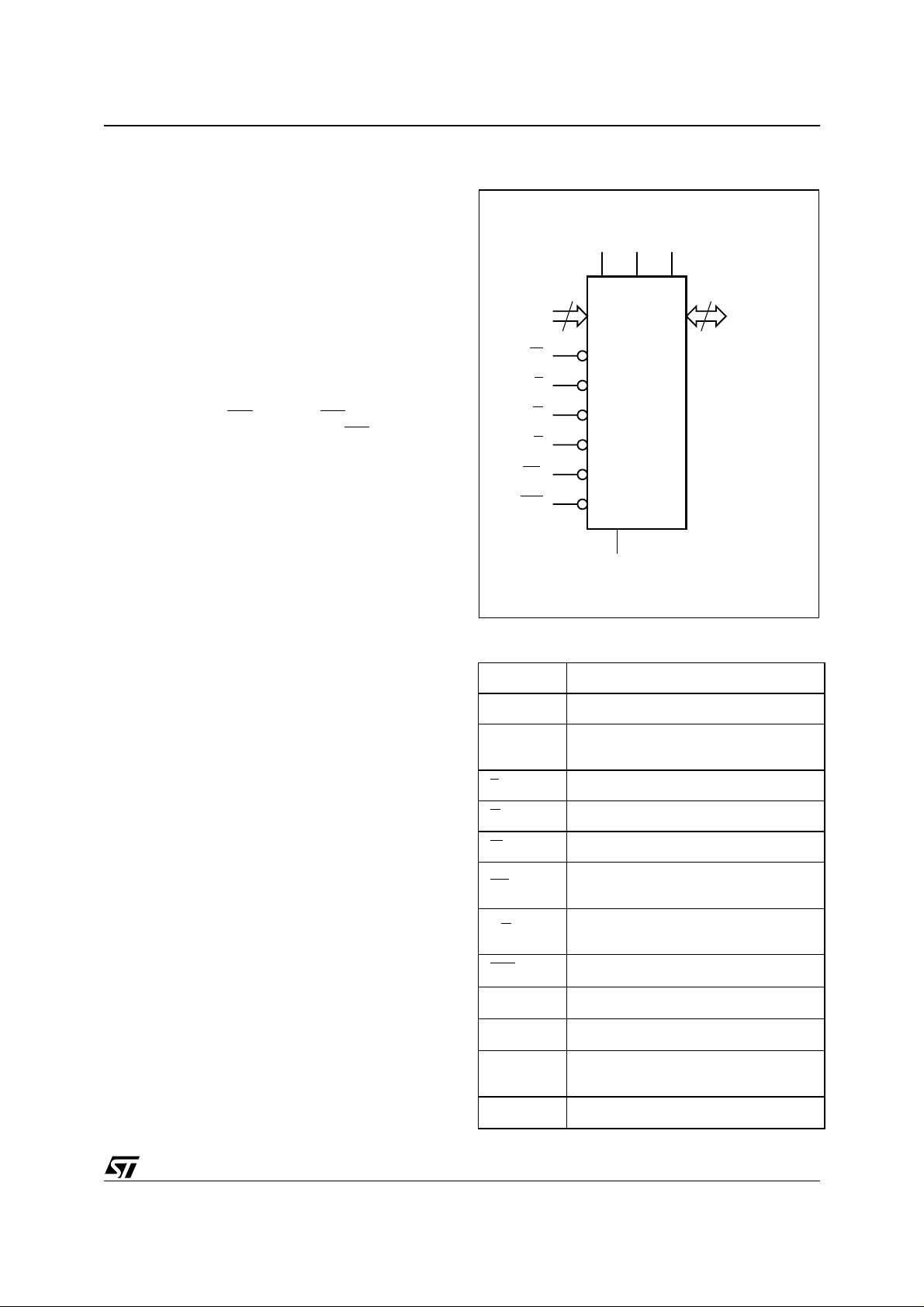
Figure 2. Logic Diagram . . . . . . . . . . . . . . . . . . . . . . . . . . . . . . . . . . . . . . . . . . . . . . . . . . . . . . . . . . 5
Table 1. Signal Names . . . . . . . . . . . . . . . . . . . . . . . . . . . . . . . . . . . . . . . . . . . . . . . . . . . . . . . . . . . 5
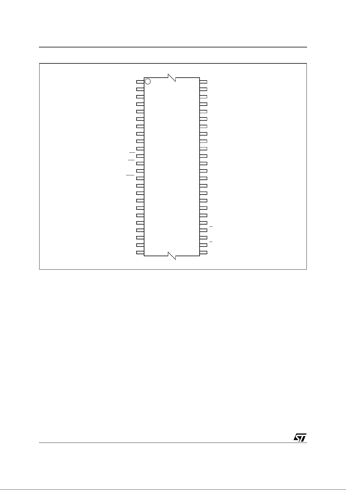
Figure 3. TSOP Connections . . . . . . . . . . . . . . . . . . . . . . . . . . . . . . . . . . . . . . . . . . . . . . . . . . . . . . . 6
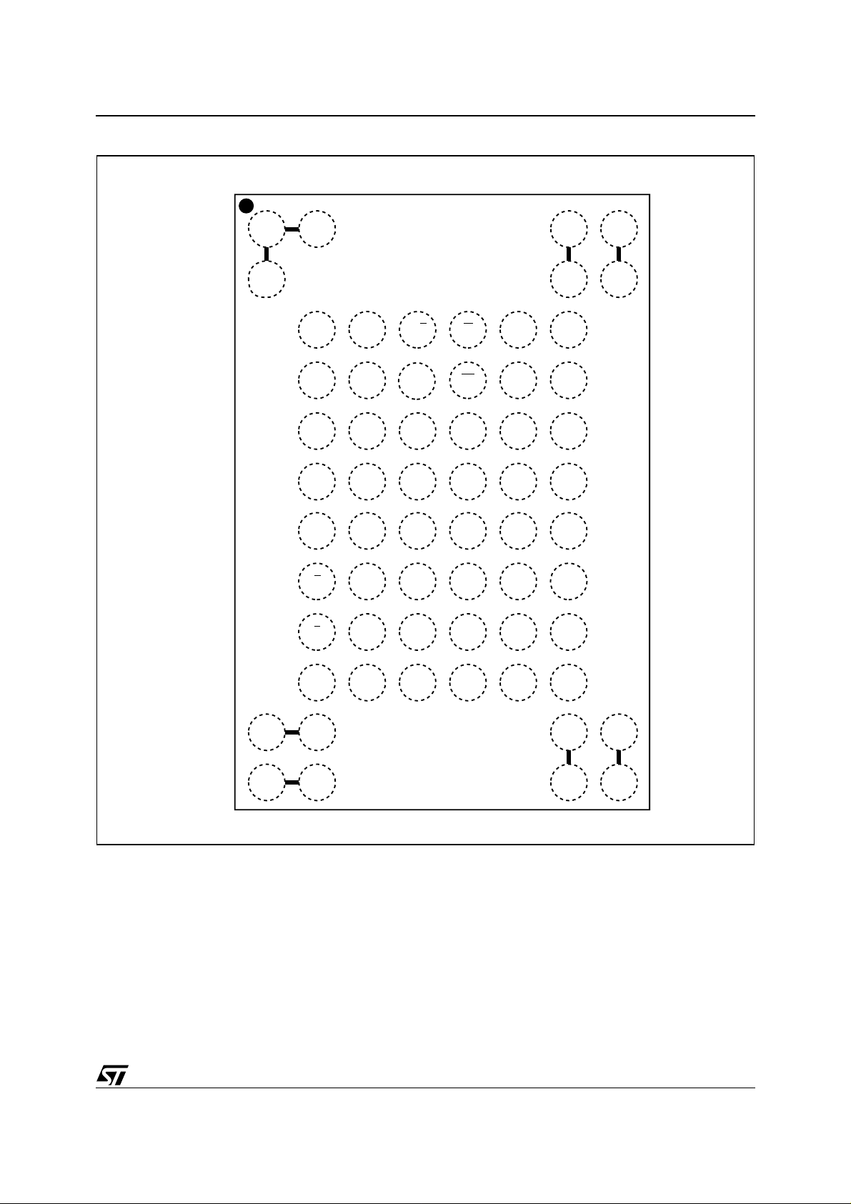
Figure 4. TFGBA Connections (Top view through package). . . . . . . . . . . . . . . . . . . . . . . . . . . . . . . 7
SIGNAL DESCRIPTIONS . . . . . . . . . . . . . . . . . . . . . . . . . . . . . . . . . . . . . . . . . . . . . . . . . . . . . . . . . . . . 8
Address Inputs (A0-A21). . . . . . . . . . . . . . . . . . . . . . . . . . . . . . . . . . . . . . . . . . . . . . . . . . . . . . . . . . 8
Data Inputs/Outputs (DQ0-DQ7). . . . . . . . . . . . . . . . . . . . . . . . . . . . . . . . . . . . . . . . . . . . . . . . . . . . 8
Data Inputs/Outputs (DQ8-DQ15 ). . . . . . . . . . . . . . . . . . . . . . . . . . . . . . . . . . . . . . . . . . . . . . . . . . . 8
Chip Enable (E). . . . . . . . . . . . . . . . . . . . . . . . . . . . . . . . . . . . . . . . . . . . . . . . . . . . . . . . . . . . . . . . . 8
Output Enable (G). . . . . . . . . . . . . . . . . . . . . . . . . . . . . . . . . . . . . . . . . . . . . . . . . . . . . . . . . . . . . . . 8
Write Enable (W). . . . . . . . . . . . . . . . . . . . . . . . . . . . . . . . . . . . . . . . . . . . . . . . . . . . . . . . . . . . . . . . 8
Write Protect (WP). . . . . . . . . . . . . . . . . . . . . . . . . . . . . . . . . . . . . . . . . . . . . . . . . . . . . . . . . . . . . . . 8
Reset/Block Temporary Unprotect (RP).. . . . . . . . . . . . . . . . . . . . . . . . . . . . . . . . . . . . . . . . . . . . . .8
V
(VPP). . . . . . . . . . . . . . . . . . . . . . . . . . . . . . . . . . . . . . . . . . . . . . . . . . . . . . . . . . . . . . . . . . . . . . 8
PP
Supply Voltage (2.7V to 3.6V).. . . . . . . . . . . . . . . . . . . . . . . . . . . . . . . . . . . . . . . . . . . . . . . . . . 8
V
CC
V
Supply Voltage (1.8V to 3.6V). . . . . . . . . . . . . . . . . . . . . . . . . . . . . . . . . . . . . . . . . . . . . . . . . 8
CCQ
V
Ground. . . . . . . . . . . . . . . . . . . . . . . . . . . . . . . . . . . . . . . . . . . . . . . . . . . . . . . . . . . . . . . . . . . . 9
SS
Table 2. Bus Operations . . . . . . . . . . . . . . . . . . . . . . . . . . . . . . . . . . . . . . . . . . . . . . . . . . . . . . . . . . 9
BUS OPERATIONS. . . . . . . . . . . . . . . . . . . . . . . . . . . . . . . . . . . . . . . . . . . . . . . . . . . . . . . . . . . . . . . . 10
Bus Read. . . . . . . . . . . . . . . . . . . . . . . . . . . . . . . . . . . . . . . . . . . . . . . . . . . . . . . . . . . . . . . . . . . . . 10
Bus Write. . . . . . . . . . . . . . . . . . . . . . . . . . . . . . . . . . . . . . . . . . . . . . . . . . . . . . . . . . . . . . . . . . . . . 10
Output Disable. . . . . . . . . . . . . . . . . . . . . . . . . . . . . . . . . . . . . . . . . . . . . . . . . . . . . . . . . . . . . . . . . 10
Standby. . . . . . . . . . . . . . . . . . . . . . . . . . . . . . . . . . . . . . . . . . . . . . . . . . . . . . . . . . . . . . . . . . . . . . 10
Automatic Standby. . . . . . . . . . . . . . . . . . . . . . . . . . . . . . . . . . . . . . . . . . . . . . . . . . . . . . . . . . . . . . 10
Special Bus Operations . . . . . . . . . . . . . . . . . . . . . . . . . . . . . . . . . . . . . . . . . . . . . . . . . . . . . . . . 10
Electronic Signature. . . . . . . . . . . . . . . . . . . . . . . . . . . . . . . . . . . . . . . . . . . . . . . . . . . . . . . . . . . . . 10
Block Protect and Chip Unprotect. . . . . . . . . . . . . . . . . . . . . . . . . . . . . . . . . . . . . . . . . . . . . . . . . . 10
Block Protect and Chip Unprotect. . . . . . . . . . . . . . . . . . . . . . . . . . . . . . . . . . . . . . . . . . . . . . . . . . 10
COMMAND INTERFACE . . . . . . . . . . . . . . . . . . . . . . . . . . . . . . . . . . . . . . . . . . . . . . . . . . . . . . . . . . . 11
Read/Reset Command . . . . . . . . . . . . . . . . . . . . . . . . . . . . . . . . . . . . . . . . . . . . . . . . . . . . . . . . . . 11
Auto Select Command. . . . . . . . . . . . . . . . . . . . . . . . . . . . . . . . . . . . . . . . . . . . . . . . . . . . . . . . . . . 11
Program Command. . . . . . . . . . . . . . . . . . . . . . . . . . . . . . . . . . . . . . . . . . . . . . . . . . . . . . . . . . . . . 11
Unlock Bypass Command. . . . . . . . . . . . . . . . . . . . . . . . . . . . . . . . . . . . . . . . . . . . . . . . . . . . . . . . 12
Unlock Bypass Program Command . . . . . . . . . . . . . . . . . . . . . . . . . . . . . . . . . . . . . . . . . . . . . . . .12
Unlock Bypass Reset Command. . . . . . . . . . . . . . . . . . . . . . . . . . . . . . . . . . . . . . . . . . . . . . . . . . .12
Chip Erase Command. . . . . . . . . . . . . . . . . . . . . . . . . . . . . . . . . . . . . . . . . . . . . . . . . . . . . . . . . . . 12
Block Erase Command . . . . . . . . . . . . . . . . . . . . . . . . . . . . . . . . . . . . . . . . . . . . . . . . . . . . . . . . . . 12
Erase Suspend Comma nd . . . . . . . . . . . . . . . . . . . . . . . . . . . . . . . . . . . . . . . . . . . . . . . . . . . . . . . 13
Erase Resume Command. . . . . . . . . . . . . . . . . . . . . . . . . . . . . . . . . . . . . . . . . . . . . . . . . . . . . . . . 13
2/42
Page 3

M29W641DH, M29W641DL, M29W641DU
Enter Extended Block Command . . . . . . . . . . . . . . . . . . . . . . . . . . . . . . . . . . . . . . . . . . . . . . . . . .13
Exit Extended Block Command. . . . . . . . . . . . . . . . . . . . . . . . . . . . . . . . . . . . . . . . . . . . . . . . . . . . 13
Table 3. Commands . . . . . . . . . . . . . . . . . . . . . . . . . . . . . . . . . . . . . . . . . . . . . . . . . . . . . . . . . . . . 14
Table 4. Program, Erase Times and Program, Erase Enduranc e Cyc les . . . . . . . . . . . . . . . . . . . . 14
STATUS REGISTER. . . . . . . . . . . . . . . . . . . . . . . . . . . . . . . . . . . . . . . . . . . . . . . . . . . . . . . . . . . . . . . 15
Data Polling Bit (DQ7). . . . . . . . . . . . . . . . . . . . . . . . . . . . . . . . . . . . . . . . . . . . . . . . . . . . . . . . . . . 15
Toggle Bit (DQ6).. . . . . . . . . . . . . . . . . . . . . . . . . . . . . . . . . . . . . . . . . . . . . . . . . . . . . . . . . . . . . . . 15
Error Bit (DQ5). . . . . . . . . . . . . . . . . . . . . . . . . . . . . . . . . . . . . . . . . . . . . . . . . . . . . . . . . . . . . . . . . 15
Erase Timer Bit (DQ3). . . . . . . . . . . . . . . . . . . . . . . . . . . . . . . . . . . . . . . . . . . . . . . . . . . . . . . . . . . 15
Alternative Toggle Bit (DQ2).. . . . . . . . . . . . . . . . . . . . . . . . . . . . . . . . . . . . . . . . . . . . . . . . . . . . . . 15
Table 5. Status Register Bits. . . . . . . . . . . . . . . . . . . . . . . . . . . . . . . . . . . . . . . . . . . . . . . . . . . . . . 16
Figure 5. Data Polling Flowchart . . . . . . . . . . . . . . . . . . . . . . . . . . . . . . . . . . . . . . . . . . . . . . . . . . . 17
Figure 6. Data Toggle Flowchart. . . . . . . . . . . . . . . . . . . . . . . . . . . . . . . . . . . . . . . . . . . . . . . . . . . 17
MAXIMUM RATING. . . . . . . . . . . . . . . . . . . . . . . . . . . . . . . . . . . . . . . . . . . . . . . . . . . . . . . . . . . . . . . . 18
Table 6. Absolute Maximum Ratings. . . . . . . . . . . . . . . . . . . . . . . . . . . . . . . . . . . . . . . . . . . . . . . .18
DC and AC PARAMETERS . . . . . . . . . . . . . . . . . . . . . . . . . . . . . . . . . . . . . . . . . . . . . . . . . . . . . . . . . 19
Table 7. Operating and AC Measurement Condition s. . . . . . . . . . . . . . . . . . . . . . . . . . . . . . . . . . . 19
Figure 7. AC Measurement I/O Waveform . . . . . . . . . . . . . . . . . . . . . . . . . . . . . . . . . . . . . . . . . . . 19
Figure 8. AC Measurement Load Circuit . . . . . . . . . . . . . . . . . . . . . . . . . . . . . . . . . . . . . . . . . . . . . 19
Table 8. Device Capacitance. . . . . . . . . . . . . . . . . . . . . . . . . . . . . . . . . . . . . . . . . . . . . . . . . . . . . . 19
Table 9. DC Characteristics. . . . . . . . . . . . . . . . . . . . . . . . . . . . . . . . . . . . . . . . . . . . . . . . . . . . . . . 20
Figure 9. Read Mode AC Waveforms . . . . . . . . . . . . . . . . . . . . . . . . . . . . . . . . . . . . . . . . . . . . . . . 21
Table 10. Read AC Characteristics . . . . . . . . . . . . . . . . . . . . . . . . . . . . . . . . . . . . . . . . . . . . . . . . . 21
Figure 10. Write AC Waveforms, Write Enable Controlled . . . . . . . . . . . . . . . . . . . . . . . . . . . . . . . 22
Table 11. Write AC Characteristics, Write Enable Controlled . . . . . . . . . . . . . . . . . . . . . . . . . . . . . 22
Figure 11. Write AC Waveforms, Chip Enable Controlled . . . . . . . . . . . . . . . . . . . . . . . . . . . . . . . . 23
Table 12. Write AC Characteristics, Chip Enable Controlled . . . . . . . . . . . . . . . . . . . . . . . . . . . . . 23
Figure 12. Reset/Block Temporary Unprotect AC Waveforms . . . . . . . . . . . . . . . . . . . . . . . . . . . . 24
Table 13. Reset/Block Temporary Unprotect AC Characteristics . . . . . . . . . . . . . . . . . . . . . . . . . . 24
Figure 13. Accelerated Program Timing Waveforms. . . . . . . . . . . . . . . . . . . . . . . . . . . . . . . . . . . . 24
PACKAGE MECHANICAL . . . . . . . . . . . . . . . . . . . . . . . . . . . . . . . . . . . . . . . . . . . . . . . . . . . . . . . . . . 25
Figure 14. TSOP48 – 48 lead Plastic Thin Small Outline, 12 x 20mm, Package Outline . . . . . . . . 25
Table 14. TSOP48 – 48 lead Plastic Thin Small Outline, 12 x 20mm, Package Mechanical Data . 25
Figure 15. TFBGA63 - 7x11mm, 6x8 active ball array, 0.8mm pitch, Bottom view pac kage outline 26
Table 15. TFBGA63 - 7x11mm, 6x8 active ball array, 0.8mm pitch, Package Mechanical Data . . 26
PART NUMBERING . . . . . . . . . . . . . . . . . . . . . . . . . . . . . . . . . . . . . . . . . . . . . . . . . . . . . . . . . . . . . . . 27
Table 16. Ordering Information Scheme . . . . . . . . . . . . . . . . . . . . . . . . . . . . . . . . . . . . . . . . . . . . . 27
APPENDIX A. BLOCK ADDRESSES. . . . . . . . . . . . . . . . . . . . . . . . . . . . . . . . . . . . . . . . . . . . . . . . . . 28
Table 17. Block Addresses . . . . . . . . . . . . . . . . . . . . . . . . . . . . . . . . . . . . . . . . . . . . . . . . . . . . . . . 28
3/42
Page 4

M29W641DH, M29W641DL, M29W641DU
APPENDIX B. COMMON FLASH INTERFACE (CFI) . . . . . . . . . . . . . . . . . . . . . . . . . . . . . . . . . . . . . 32
Table 18. Query Structure Overview. . . . . . . . . . . . . . . . . . . . . . . . . . . . . . . . . . . . . . . . . . . . . . . .32
Table 19. CFI Query Identification String . . . . . . . . . . . . . . . . . . . . . . . . . . . . . . . . . . . . . . . . . . . .32
Table 20. CFI Query System Interface Information. . . . . . . . . . . . . . . . . . . . . . . . . . . . . . . . . . . . . 33
Table 21. Device Geometry Definition. . . . . . . . . . . . . . . . . . . . . . . . . . . . . . . . . . . . . . . . . . . . . . .33
Table 22. Primary Algorithm-Specific Extende d Query Table . . . . . . . . . . . . . . . . . . . . . . . . . . . . . 34
Table 23. Security Code Area . . . . . . . . . . . . . . . . . . . . . . . . . . . . . . . . . . . . . . . . . . . . . . . . . . . . . 3 4
APPENDIX C. EXTENDED MEMORY BLOCK . . . . . . . . . . . . . . . . . . . . . . . . . . . . . . . . . . . . . . . . . . 35
Factory Locked Extended Block . . . . . . . . . . . . . . . . . . . . . . . . . . . . . . . . . . . . . . . . . . . . . . . . . 35
Customer Lockable Extended Block. . . . . . . . . . . . . . . . . . . . . . . . . . . . . . . . . . . . . . . . . . . . . . 35
Table 24. Extended Block Address and Data . . . . . . . . . . . . . . . . . . . . . . . . . . . . . . . . . . . . . . . . . 35
APPENDIX D. BLOCK PROTECTION . . . . . . . . . . . . . . . . . . . . . . . . . . . . . . . . . . . . . . . . . . . . . . . . . 36
Programmer Technique . . . . . . . . . . . . . . . . . . . . . . . . . . . . . . . . . . . . . . . . . . . . . . . . . . . . . . . . 36
In-System Technique . . . . . . . . . . . . . . . . . . . . . . . . . . . . . . . . . . . . . . . . . . . . . . . . . . . . . . . . . . 3 6
Table 25. Programmer Technique Bus Operations . . . . . . . . . . . . . . . . . . . . . . . . . . . . . . . . . . . . . 36
Figure 16. Programmer Equipment Group Protect Flowchart. . . . . . . . . . . . . . . . . . . . . . . . . . . . . 37
Figure 17. Programmer Equipment Chip Unprotect Flowchart . . . . . . . . . . . . . . . . . . . . . . . . . . . . 38
Figure 18. In-System Equipment Group Protect Flowchart. . . . . . . . . . . . . . . . . . . . . . . . . . . . . . . 39
Figure 19. In-System Equipment Chip Unprotect Flowchart . . . . . . . . . . . . . . . . . . . . . . . . . . . . . .40
REVISION HISTORY. . . . . . . . . . . . . . . . . . . . . . . . . . . . . . . . . . . . . . . . . . . . . . . . . . . . . . . . . . . . . . . 41
Table 26. Document Revision History . . . . . . . . . . . . . . . . . . . . . . . . . . . . . . . . . . . . . . . . . . . . . . .41
4/42
Page 5
SUMMARY DESCRIPTION
The M29W641D is a 64 M bit (4Mb x16 ) non-volatile memory that can be read, erased and reprogrammed. These operations can be performed
CCQ
sup-
CC
supply
PP
using a single, low voltage, 2.7V to 3.6V V
ply for the circuitry and a 1.8V to 3.6V V
for the Input/Output pins. An optional 12 V V
power supply is provided to speed up customer
programming.
On power-up the memory defaults to its Read
mode where it can be read in the same way as a
ROM or EPROM.
The highest address blo ck of the M 29W641DH or
the lowest address block of th e M29W641DL c an
be protected from accidental programming or erasure using the WP
M29W641DU does not feature the WP
pin (if WP = VIL). The
pin.
Each block can be erased indep endently so it is
possible to preserve valid dat a while old data is
erased. The blocks can be protected to prevent
accidental Program or Erase commands from
modifying the memory. Program and E rase commands are written to the Command Interface of
the memory. An on-chip Program/Erase Controller
simplifies the process of prog ramming or erasing
the memory by taking care of all of the special operations that are required to update the memory
contents. The end of a program or erase operation
can be detected and any error conditions identified. The command set required to control the
memory is consistent with JEDEC standards.
The M29W641D has an extra block, the Extended
Block, (of 32 KWords) that can be accessed using
a dedicated command. The Extended Block can
be protected and so is useful for storing security
information. However the protec tion i s not re versible, once protected the protection cannot be undone.
Chip Enable, Output Enable and Write Enable signals control the bus operation of the memory.
They allow simple conne ction to most m icroprocessors, often without additional logic.
The memory is offered in a 48-pin TSOP package
(M29W641DL and M29W641DH) or in a 63- ball TFBGA package (M29W64 1DU). All de vices a re del ivered with all the bits erased (set to 1) .
M29W641DH, M29W641DL, M29W641DU
Figure 2. Logic Diagram
CCQ
V
PP
16
DQ0-DQ15
AI06697b
V
V
CC
22
A0-A21
W
E
G
RB
RP
WP
M29W641D
V
SS
Table 1. Signal Names
A0-A21 Address Inputs
DQ0-DQ7 Data Inputs/Outputs
DQ8-
DQ15
E
G
W
RP
RB
Data Inputs/Outputs
Chip Enable
Output Enable
Write Enable
Reset/Block Temporary Unprotect
(M29W641DH and M29W641DL only)
Ready/Busy Output (M29W641DU
only)
WP
V
CC
V
CCQ
V
PP
V
SS
Write Protect
Supply Voltage
Supply Voltage for Input/Output
Supply Voltage for Fast Program
(optional)
Ground
5/42
Page 6
M29W641DH, M29W641DL, M29W641DU
Figure 3. TSOP Connections
A15
A14
A13
A12
A11
1
48
A16
V
CCQ
V
SS
DQ15
DQ7
A10 DQ14
37
36
DQ6
DQ13
DQ5
DQ12
DQ4
V
CC
DQ11
DQ3
DQ10
DQ2
DQ9
DQ1
DQ8
DQ0
G
V
SS
E
A0
A21
A20
RP
V
PP
WP
A19
A18
A17
A9
A8
W
A7
A6
A5
A4
A3
A2
A1
12
M29W641D
13
24 25
AI06698
6/42
Page 7
M29W641DH, M29W641DL, M29W641DU
Figure 4. TFGBA Connections (Top view through package)
654321
A
B
NC
NC
(1)
(1)
C
D
E
F
G
H
NC
A3
A4
A2
A1
A0
(1)
A7
A17
A6
RB
V
PP
A18
A5 A20
DQ0
E
DQ8
DQ2
DQ10
W
RP
A21
A19
DQ5
DQ12
A9
A8
A10
A11
DQ7
DQ14
NC
NC
V
(1)
(1)
A13
A12
A14
A15
A16
CCQ
NC
NC
87
(1)
(1)
J
K
L
NC
M
NC
G
DQ9
V
SS
(1)
NC
(1)
NC
DQ1
(1)
(1)
DQ11
DQ3
V
CC
DQ4
Note: 1. Bal l s ar e shorted to get her via the substrate but not connec ted to the die.
DQ13
DQ6
DQ15
V
SS
NC
NC
NC
NC
(1)
(1)
AI06879
(1)
(1)
7/42
Page 8

M29W641DH, M29W641DL, M29W641DU
SIGNAL DESCRIPTIONS
See Figure 2, Logic Diagram, and T able 1, Sign al
Names, for a brief overview of the signals connected to this device.
Address Inputs (A0-A21). The Address Inputs
select the cells i n the memory array to a ccess during Bus Read operations. During Bus Write operations they control the commands sent to the
Command Interface of the Program/Erase Controller.
Data Inputs/Outputs (DQ0-DQ7). The Data I/O
outputs the data stored at the selected address
during a Bus Read operation. During Bus Write
operations they represent the commands sent to
the Command Interface of the Program/Erase
Controller.
Data Inputs/Outputs (DQ8-DQ15). The Data I/O
outputs the data stored at the selected address
during a Bus Read operation. During Bus Write
operations the Command Register does not use
these bits. When reading the Status Register
these bits should be ignored.
Chip Enable (E
the memory, allowing Bus Read and Bus Write operations to be performed. When Chip Enable is
High, V
IH
Output Enable (G
trols the Bus Read operation of the memory.
Write Enable (W
the Bus Write operation of the memory’s Command Interf a c e .
Write Protect (W
available in the M29W641DH and M29W641DL
only. I t provid es a hard ware metho d of pro t ecting
the highest address block for the M29W641DH
and the lowest address block for the
M29W64 1DL. The Write Protect pin must not be
left floating or unconnected.
When Write Protect is Low, V
tects either the highest or low est address block;
Program and Erase operations in this block are ignored while Write Protect is Low.
When Write Pr otect
verts to the previous protection status for this
block. Program and Erase operations can now
modify the data in t his block unless the block is
protected using Block Protection.
Ready/Busy Output (RB
is an open-drain output that can be used to identify
when the device is performing a Program or Erase
operation. During Program or Erase operations
Ready/Busy is Low, V
pedance during Read mode, Auto Select mode
and Erase Suspend mode.
After a Hardware Reset, Bus Read and Bus Write
operations cannot begin until Ready/Busy be-
). The Chip Enable, E, activates
, all other pins are ignored.
). The Output Enable, G, con-
). The Write Enable, W, controls
P). The Write Protect pin is
, the memory pro-
IL
is High, VIH, the memory re-
). The Ready/Busy pin
. Ready/Busy is high-im-
OL
comes high-impedance. See Tabl e 13 and Figure
12, Reset/Block Temporary Unprotect AC Characteristics.
The use of an open-drain output allows the Ready/
Busy pins from several memories to be connected
to a single pull-up resistor. A Low will then indicate
that one, or more, of the memories is busy.
Reset/Block Temporary Unprotect (RP
). The
Reset/Block Temporary Unprotect pin can be
used to apply a Hardware Reset to the memory or
to temporarily unprotect all Blocks that hav e b een
protected.
Note that if Write Protect
(WP) is at VIL, then one
of the two outermost blocks will remain p rotected
even if RP is at V
.
ID
A Hardware Reset is achieved by holding Reset/
Block Temporary Unprotect Low, V
. After Reset/Block Temporary Unprotect
t
PLPX
goes High, V
, the memory will be ready for Bus
IH
Read and Bus Write operations after t
t
, whichever occurs las t. See Table 13 and
RHEL
, for at least
IL
PHEL
or
Figure 12, Reset/Block T emporary Unprotect AC
Characteristics, for more details.
Holding RP
at VID will temporarily unprotect the
protected Blocks in the memory. Program and
Erase operations on all blocks will be possible.
The transition from V
t
V
.
PHPHH
(VPP). When the VPP pin is raised to V
PP
to VID must be slower than
IH
PPH
the memory automatically enters the Unlock Bypass mode. When the pin is returned to V
IH
or V
normal operation resumes. During Unlock Bypass
Program operations the memory draws I
PP
from
the pin to supply the programming circuits. See the
description of the Unlock Bypass comm and in the
Command Interface section. The transitions from
V
to VPP and from VPP to VIH must be slower
IH
than t
Never raise the pin to V
, see Figure 13.
VHVPP
from any mode except
PP
Read mode, otherwise the memory may be left in
an indeterminate state.
V
Supply Voltage (2.7V to 3.6V). VCC pro-
CC
vides the power supply for all operations (Read,
Program and Erase).
The Command Interface is disabled when the V
CC
Supply Voltage is less than the L ockout Voltage,
. This prevents Bus Write operations from ac-
V
LKO
cidentally damaging the data during power up,
power down and power surges. If the Program/
Erase Controller is programming or erasing during
this time then the operation aborts and the memory contents being altered will be invalid.
V
Supply Voltage (1.8V to 3.6V). V
CCQ
CCQ
provides the power supply to the I/O pins and enables
all Outputs to be powered indepen dently of V
CC
IL
.
8/42
Page 9
M29W641DH, M29W641DL, M29W641DU
V
can be tied to VCC or can use a separate
CCQ
supply.
V
Ground. VSS is the reference for all voltage
SS
measurements. The device f eatu res two V
SS
pins
which must be both connected to the system
ground.
Note: Each device in a system should have
V
CC, VCCQ
and VPP decoupled from V
SS
with a
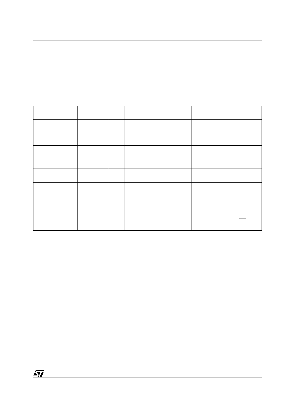
Table 2. Bus Operations
Operation E G W
Bus Read
Bus Write
Output Disable X
Standby
Read Manufacturer
Code
Read Device Code
Extended Memory
Block Verify Code
Note: X = VIL or VIH.
V
V
V
V
V
V
V
IL
V
IL
V
IH
V
IL
V
IL
V
IL
V
IL
IH
IH
Cell Address Data Output
IH
V
Command Address Data Input
IL
V
X Hi-Z
IH
X X X Hi-Z
A0 = VIL, A1 = VIL, A9 = VID,
V
IL
IL
IL
IH
Others V
A0 = VIH, A1 = VIL, A9 = VID,
V
IH
Others V
A0 = VIH, A1 = VIH, A6 = VIL,
V
IH
A9 = V
0.1µF ceramic capacitor close to the pin for
current surge protection (high frequency, inherently low inductance ca pacitors should b e
as close as possible to the device). See Figure
8, AC Measurement Load Circuit. The PCB
trace widths should be sufficient to carry the
required V
program and erase curr ents. S ee
PP
Table 9, DC Characteristics.
Address Inputs
A0-A21
or V
IL
IH
or V
IL
IH
, Others VIL or V
ID
IH
Data Inputs/Outputs
DQ15-DQ0
0020h
22C7h
98h (factory locked, WP protects
highest address block)
18h (not factory locked, WP
protects highest address
block)
88h (factory locked, WP
lowest block)
08h (not factory locked, WP
protects lowest block)
protects
9/42
Page 10

M29W641DH, M29W641DL, M29W641DU
BUS OPERATIONS
There are five standard bus operations that control
the device. These are Bus Read, Bus Wri te, Output Disable, Standby and Automatic Standby. See
Table 2, Bus Operations, for a summary. Typically
glitches of less than 5ns on Chip Enabl e o r Write
Enable are ignored by t he mem ory and do not a ffect bus operations.
Bus Read. Bus Read operations read from the
memory cells, or specific registers in the Command Interface. A valid Bus Read operation involves setting the desired address on the Address
Inputs, applying a Low sig nal, V
and Output Enable and keeping Write Enable
High, V
. The Data Inputs/Outputs will output the
IH
value, see Figure 9, Read Mode AC W aveforms,
and Table 10, Read AC Characteristics, for details
of when the output becomes valid.
Bus Write. Bus Write operations write to the
Command Interface. A valid Bus Write operation
begins by setting the desire d address on t he Address Inputs. The Address Inputs are latched by
the Command Interface on the falling edge of Chip
Enable or Write Enable, whichever occurs last.
The Data Inputs/Outputs a re latched by the Command Interface on the rising edge of Chip Enable
or Write Enable, whichever occurs first. Output Enable must remain High, V
IH
Write operation. See Figure 10 and Figure 11,
Write AC Waveforms, and Table 11 and Table 12,
Write AC Characteristics, for details of the timing
requirements.
Output Disa bl e . The Data Inputs/Outputs are in
the high impedance s tate when Output Enable is
High, V
.
IH
Standby. When Chip Enable is High, V
memory enters Standby mode and the Data Inputs/Outputs pins are placed in the high-impedance state. To reduce the S upply Current to the
Standby Supply Current, I
CC2
, to Chip Enable
IL
, during the whole Bus
, the
IH
, Chip Enable should
be held within V
± 0.2V. For the Standby current
CC
level see Table 9, DC Characteristics.
During program or erase operations the memory
will continue to use the Program/Erase Supply
Current, I
, for Program or Erase operations un-
CC3
til the operation completes.
Automatic Standby. If CMOS levels (V
± 0.2V)
CC
are used to drive the bus and the bus is inactive for
300ns or more the memory enters Automatic
Standby where the internal Supply Current is reduced to the Standby Supply Current, I
CC2
. The
Data Inputs/Outputs will still output data if a Bus
Read operation is in progress.
Special Bus Operations
Additional bus operations can be performed to
read the Electronic Signature and also to apply
and remove Block Protec tion. These bus operations are intended for use by programming equipment and are not usually used in applications.
They require V
to be applied to some pins.
ID
Electronic Signature. The memory has two
codes, the manufacturer code and the device
code, that can be read to identify the memory.
These codes can be read by applying t he signals
listed in Table 2, Bus Operations.
Block Protect and Chip Unprotect.
Groups of
blocks can be protected against accidental Program or Erase. The whole chip can be unprotected
to allow the data inside the blocks to be changed.
Write Protect
the outermost blocks. When Write Protect
at V
one of the two outer mos t blo cks is protect-
IL
(WP) can be used to protect one of
(WP) is
ed and r emai ns prote cte d r egar dle ss o f th e Bloc k
Protection Status or the Reset/Block Temporary
Unprotect pin statu s. For the M 29W641D H, it is
the highest addressed block that can be protected. For th e M29W 641DL, it i s t he l owest.
Block Protect and Chip Unprote ct operations are
described in Appendix D.
10/42
Page 11

COMMAND INTERFACE
All Bus Write operations t o the me mory are in terpreted by the Command Interface. Commands
consist of one or more sequential Bus Write operations. Failure to observe a valid sequence of Bus
Write operations will result in the memory returning to Read mode. The long command sequences
are imposed to maximize data security.
See Table 3 for a summary of the commands.
Read/Reset Command
The Read/Reset command returns the memory to
its Read mode where it behaves like a ROM or
EPROM. It also resets the errors in the Status
Register. Either one or three Bus Write operations
can be used to issue the Read/Reset command.
The Read/Reset command can be issued, between Bus Write cycles before the start of a program or erase operation, to return the device to
read mode. If the Read/Reset command is issued
during the timeout of a Block erase operation then
the memory will take up to 10µs to abort. During
the abort period no valid data can be read from the
memory. The Read/Reset command will not abort
an Erase operation when issued while in Erase
Suspend.
Auto Select Command
The Auto Select command is used to read the
Manufacturer Code, the Device Code , the Block
Protection Status and the Extended Memory Block
Verify Code. Three consecutive B us Write operations are required to iss ue the Auto Select command. Once the Auto Select command is issued
the memory remains in Auto Select mode until a
Read/Reset command is issued. Read CFI Query
and Read/Reset comma nds are ac cept ed i n Aut o
Select mode, all other commands are ignored.
In Auto Select mode the Manufac turer Code can
be read using a Bus Read operation with A0 = V
and A1 = VIL. The other address bits may be set to
either V
or VIH. The Manufacturer Code f or ST-
IL
Microelectronics is 0020h.
The Device Code can be read using a B us Read
operation with A0 = V
address bits may be set to e ither V
and A1 = VIL. The other
IH
or VIH. The
IL
Device Code for the M29W641D is 22C7h.
The Bl ock Prot ection S tatus of each block can be
read using a Bus Read operation with A0 = V
A1 = V
, and A 12 -A 21 spec ify i n g t he address of
IH
IL
the bl ock. The oth er addr ess bit s may b e set t o either V
or VIH. If t h e ad dr ess ed b loc k is pro tec te d
IL
then 01h is output on Data Inputs/Outputs DQ0DQ7, otherwise 00h is output.
Read CFI Query Command
The Read CFI Query Command is used to read
data from the Common Flash Interface (CFI)
Memory Area. This command is valid when the de-
M29W641DH, M29W641DL, M29W641DU
vice is in the Read Array mode, or when the device
is in Autose lec ted mode .
One Bus Write cycle is required to issue the Read
CFI Query Command. Once the command is issued subsequent Bus Read ope rations read from
the Common Flash Interface Memory Area.
The Read/Reset command m ust be issued to return the device to the previous mode (the Read Array mode or Autoselected mode). A second Read/
Reset command would be needed if the device is
to be put in the Read Array mode from Autoselected mode.
See Appendix B, Table 18 to Table 23 for details
on the information contained in the Common Flash
Interface (CFI) memory area.
Program Command
The Program command can be used to program a
value to one address in the memory array at a
time. The command requires four Bus Write operations, the final write operation latches the address and data, and starts the Program/Erase
Controller.
If the address falls in a pro tected block then the
Program command is ignored, the data remains
unchanged. The Status Register is never read and
no error condition is given.
During the program operat ion the memo ry will ignore all commands. I t is n ot poss ible t o iss ue any
command to abort or pause the operation. Typical
program times are given in Table 4. Bus Read operations during the program o peration will output
the Status Register on the Data Inputs/Outputs.
See the section on the S tatus Register for more
details.
After the program operation has completed the
memory will return to the Read mode, unle ss an
IL
error has occurred. When an error occurs the
memory will continue to output the Status Register. A Read/Reset command must be issued to reset the error condition and return to Read mode.
Note that the Program command cannot change a
bit set at ’0’ bac k to ’1’. One of the E rase Commands must be used to set all the bits in a block or
in the whole memory from ’0’ to ’1’.
Fast Program Commands
,
There is a Fast Program command available to improve the programming throughput, by writing several adjacent words or bytes in parallel: the Double
Word Program command.
Double Word Program Command. Th e D oub l e
Word Program command is used to write a p age
of two adjacent words in parallel. Th e two words
must differ only for the address A0.
Three bus write cycles are necessary to issue the
Double Word Program command.
11/42
Page 12

M29W641DH, M29W641DL, M29W641DU
■ The first bus cycle sets up the Double Word
Program Command.
■ The second bus cycle latches the Address and
the Data of the first word to be written.
■ The third bus cycle latches the Address and the
Data of the second word to be written and starts
the Program/Erase Controller.
Only one bank can be programmed at any one
time. The other b ank must be in Read mode or
Erase Suspend.
Programming should not be attempted when V
is not at V
PPH
.
PP
After programming has started, Bus Read operations in the Bank being programmed output the
Status Register content, while Bus Read operations to the other B ank outpu t the cont ents of t he
memory ar ray.
After the program operation has completed the
memory will return to the Read mode, unle ss an
error has occurred. When an error occurs Bus
Read operations to the Bank where the command
was issued will continue to output the Status Register. A Read/Reset command must be issued to
reset the error condition and return t o Read mode.
Note that the Fast Program commands cannot
change a bit set at ’0’ back to ’1’. One of the Erase
Commands must be used to set all the bits in a
block or in the whole memory from ’0’ to ’1’.
Typical Program times are given in Tab le 4, Program, Erase Times and Program, Erase Endurance Cycles.
Unlock Bypass Command
The Unlock Bypass command is used in conjunction with the Unlock Bypass Program command to
program the memory faster than with the standard
program commands. When th e cycle time to the
device is long (as with some EPROM programmers) considerable time saving can be m ade by
using these commands. Three Bus Write operations are required to issue the Unlock Bypass
command.
Once the Unlock Bypas s command has bee n issued the memory enters Unlock Bypass mode.
When in this mode the memory can be read as if
in Read mode.
When V
is applied to the VPP pin the memory
PPH
automatically enters the Unlock Bypass mode and
the Unlock Bypass Program command can be issued immediately.
Unlock Bypass Program Command
The Unlock Bypass Program command can be
used to program one address in the memory array
at a time. The command requires two B us Write
operations, the final write operation latches the ad-
dress and data, and starts the Program/Erase
Controller.
A Program operation initiated by issuing the Unlock Bypass Program command is identical to a
Program operation initiated by issuing the Program command. I t cannot be abo rted and a Bus
Read operation will output the Status Register.
See the Program Comma nd paragrap h f or further
details.
Unlock Bypass Reset Command
The Unlock Bypass Rese t command can be used
to return to Read/Reset mode from Unlock Bypass
Mode. Two Bus Write operations are required to
issue the Unlock Bypass Reset command. Read/
Reset command does not exit from Unlock Bypass
Mode.
Chip Erase Command
The Chip Erase command can be used to erase
the entire chip. Six Bus Write operations a re required to issue the Chip Erase Command and start
the Program/Erase Controller.
If any blocks are protected then these are ignored
and all the other blocks are erased. If all of the
blocks are protect e d th e Chip Erase op erat i on appears to start but will terminate within about 100µs,
leaving the data unchanged. No error condition is
given when protected blocks are ignored.
During the erase operation the memory will ignore
all commands, including the Erase Suspen d command. It is not possible to i ssue any c ommand t o
abort the operation. Typical chip erase tim es are
given in Table 4. All Bus Read operations during
the Chip Erase operation will output the Status
Register on the Data Inputs/Outputs. See the section on the Status Register for more details.
After the Chip Erase operation has completed t he
memory will return to the Read Mode, unle ss an
error has occurred. When an error occurs the
memory will continue to output the Status Register. A Read/Reset command must be issued to reset the error condition and return to Read Mode.
The Chip Erase Command sets all of the bits in unprotected blocks of the memory to ’1’. All previous
data is lost.
Block Erase Command
The Block Erase com mand can be used to erase
a list of one or more blocks. Six Bus Write operations are required to select the first block in the li st.
Each additional block in the list can be selected by
repeating the sixth Bus Write operation using the
address of the additional block. The B lock Erase
operation starts the Program/Erase Controller
about 50µs after the last Bus Write operation.
Once the Pr ogram /Erase Co ntroller st arts it is not
possible to select any more blocks. Each additional block must therefore be selected within 50µs of
12/42
Page 13

M29W641DH, M29W641DL, M29W641DU
the lowest address block. The 50µs timer restarts
when an additional block is selected. The Status
Register can be read after the sixth Bus Write operation. See the Status Register section for details
on how to identify if th e Program /Erase Controller
has started the Block Erase operation.
If any selected blocks are protected then these are
ignored and all the other selected blocks are
erased. If all of the selected blocks are p rotected
the Block Erase operation appears to start but will
terminate within about 100µs, leaving the data unchanged. No error condition is given when protected blocks are ignored.
During the Block Erase operation the me mory wi ll
ignore all commands except the Erase Susp end
command. Typical b lock era se tim es are g iven in
Table 4. All Bus Read operations during the Block
Erase ope ra tion will outp ut the S t atus R e gister on
the Data Inputs/Outputs. See the section on the
Status Register for more details.
After the Block Erase operation has completed the
memory will return to the Read Mode, unle ss an
error has occurred. When an error occurs the
memory will continue to output the Status Register. A Read/Reset command must be issued to reset the error condition and return to Read mode.
The Block Erase Command sets all of the bits in
the unprotected selected blocks to ’1’. All previous
data in the selected blocks is lost.
Erase Suspend Command
The Erase Suspend Command may be used to
temporarily suspend a B lock Eras e operation and
return the memory to Read mode. T he comm and
requires one Bus Write operation.
The Program/Erase Controller will sus pend within
the Erase Suspend Latency time of the Erase Suspend Command being issued. Once the Program/
Erase Controller has stopped the mem ory will be
set to Read mode and the E ras e wi ll be s uspended. If the Erase Suspend command is issued during the period when the memory is waiting for an
additional block (before the Program/Er ase Controller starts) then the Erase is suspended immediately and will start immediately when the Erase
Resume Command is issued. It is not possibl e to
select any further blocks to erase after the Erase
Resume.
During Erase Suspend it is possible to Read and
Program cells in blocks that are not being erased;
both Read and Program operations behave as
normal on these blocks. If any attempt is made to
program in a protected block or in the suspended
block then the Program comm and is ignored and
the data remains unchanged. The Status Register
is not read and no error condi tion is given. Reading from blocks that are being erased will output
the Status Register.
It is also possible to issue the Auto Select, Read
CFI Query and Unlock Bypass commands du ring
an Erase Suspend. The Read/Reset command
must be issued to return the device to Read Array
mode before the Resume command will be accepte d.
Erase Resume Command
The Erase Resume command must be used to restart the Program/Erase Controller after an Erase
Suspend. The device must be in Read Array mode
before the Resume command will be accepted. An
erase can be suspe nded and resumed mo re t han
once.
Enter Extended Block Command
The device has an extra 32 KWord block (Extended Block) that can only be accessed using the Enter Extended Block command. Three Bus write
cycles are required to issue the Exte nded Block
command. Once the command has been issued
the device enters Extended B lock mo de where all
Bus Read or Write operations to the Boot Block
addresses access the Extended Block. The Extended Block (with the same address as the Boot
Blocks) cannot be erased, and can be t reated as
one-time programmable (OTP) memory. In Extended Block mode the Boot Blocks are not accessible.
To exit from the Extended Block mode the Exit Extended Block command must be issued.
The Extended Block can be protected, however
once protected the protection cannot be undone.
Exit Extended Block Com m a n d
The Exit Extended Block command is used to exit
from the Extended Block mod e and ret urn the device to Read mode. Four Bus Write operations are
required to issue the command.
Block Protect and Chip Unprotect Commands
Groups of blocks can be protected against acci-
dental Program or E rase. The whole chip can be
unprotected to allow the data i nside the blocks to
be changed.
Block Protect and Chip Unprote ct operations are
described in Appendix D.
13/42
Page 14

M29W641DH, M29W641DL, M29W641DU
Table 3. Commands
Bus Write Operations
Command
1X F0
Read/Reset
3 555 AA 2AA 55 X F0
Auto Select 3 555 AA 2AA 55 555 90
Program 4 555 AA 2AA 55 555 A0 PA PD
Double Word Program 3 555 50 PA0 PD0 PA1 PD1
Unlock Bypass 3 555 AA 2AA 55 555 20
1st 2nd 3rd 4th 5th 6th
Length
Addr Data Addr Data Addr Data Addr Data Addr Data Addr Dat a
Unlock Bypass
Program
2X A0PAPD
Unlock Bypass Reset 2 X 90 X 00
Chip Erase 6 555 AA 2AA 55 555 80 555 AA 2AA 55 555 10
Block Erase 6+ 555 AA 2AA 55 555 80 555 AA 2AA 55 BA 30
Erase Suspend 1 X B0
Erase Resume 1 X 30
Read CFI Query 1 55 98
Enter Extended Block 3 555 AA 2AA 55 555 88
Exit Extended Block 4 555 AA 2AA 55 555 90 X 00
Note: X Do n’ t Care, PA P rogram Address, PD Pro gram Data , B A Any address in the Block. All values i n the table are i n hexadecim al .
Table 4. Program, Erase Times and Progra m , Erase Endurance Cycles
Parameter Min
Typ
(1, 2)
Chip Erase 80
Block Erase (32 KWords) 0.8
Erase Suspend Latency Time
Program (Word) 10
Double Word Program 10
Chip Program (Word by Word) 40
Chip Program (Double Word) 20
Program/Erase Cycles (per Block) 100,000 cycles
Data Retention 20 years
Note: 1. Typical value s m easured at room temp erature and nominal vol t ages.
2. Sampled, but not 100% tested.
3. Maximum value measu red at worst cas e conditio ns for both temperature an d V
4. Maximum value measu red at worst cas e conditio ns for both temperature an d V
after 100,0 0 program/erase cycle s.
CC
.
CC
Max
400
6
50
200
200
200
100
(4)
(4)
(3)
(3)
(3)
(3)
(3)
(2)
Unit
s
s
µs
µs
µs
s
s
14/42
Page 15

STATUS REGISTER
Bus Read operations from any address always
read the Status Register during Program and
Erase operations. It is also read during Erase Suspend when an address within a block being erased
is accessed.
The bits in the Status Register are summarized in
Table 5, Status Register Bits.
Data Polling Bit (DQ7). The Data Polling Bit can
be used to identify whether the Program/Erase
Controller has successfully completed its operation or if it has responded to an Erase Suspend.
The Data Polling Bit is output on DQ7 when the
Status Register is read.
During Program operations the Data Polling Bit
outputs the complement of the bit being programmed to DQ7. After successful completion of
the Program operation the memory returns to
Read mode and Bus Read operations from the address just programmed o utput DQ7, not its complement.
During Er ase ope rations the Data Polling Bit ou t-
puts ’0’, the complement of the erased state of
DQ7. After successful completion of the Erase operation the memory returns to Read Mode.
In Erase Suspend mode the Data Polling Bit will
output a ’1’ during a Bus Read operation within a
block being erased. The Data Polling Bit will
change from a ’0’ to a ’1’ when the Program/Erase
Controller has suspended the Erase operation.
Figure 5, Data Polling Flowchart, gives an example of how to use the Data Polling Bit. A Valid Address is the address being programmed or an
address within the block being erased.
Toggle Bit (DQ6). The Toggle Bit can be used to
identify whether the Program/Erase Controller has
successfully completed its operation or if it has responded to an Erase Suspen d. The Toggle Bit is
output on DQ6 when the Status Register is read.
During Program and Erase operations the Toggle
Bit changes from ’0’ to ’ 1’ to ’ 0’, et c., with su ccessive Bus Read operations at any address. After
successful completion of the operation the memory returns to Read mode.
During Erase Suspend mode the Toggle Bit will
output when addressing a cell within a block being
erased. The Toggle Bit will stop toggling when the
Program/Erase Controller has suspended the
Erase operation.
Figure 6, Dat a Toggle Flowchart, gives an example of how to use the Data Toggle Bit.
M29W641DH, M29W641DL, M29W641DU
Error Bit (DQ5). The Error Bit can be used to
identify errors detected by the Program/Erase
Controller. The Error B it is set to ’1’ when a Program, Block Erase or Chip Erase operation fails to
write the correct data to the memory. If the Error
Bit is set a Read/Rese t command must be iss ued
before other commands are issued. The E rror bit
is output on DQ5 when the Status Register is read.
Note that the Program command cannot change a
bit set to ’0’ back to ’1’ and attempting to do so will
set DQ5 to ‘1’. A Bus Read operation to that address will s h ow the bit is s ti ll ‘0’. One o f t he E r as e
commands must b e used to set all the bits in a
block or in the whole memory from ’0’ to ’1’.
Erase Timer Bit (DQ3). The Erase Timer Bit can
be used to identify the start of Program/Erase
Controller operation during a Block Erase command. Once the Program/Erase Controller starts
erasing the Erase Timer Bit is set to ’1’. Before the
Program/Erase Controller starts the Erase Timer
Bit is set to ’0’ and additional block s to be erased
may be written to the Command Interface. The
Erase Timer Bit is output on DQ3 when the Status
Register is read.
Alternative Toggle Bit (DQ2). The Alternative
Toggle Bit can be used to monitor the Program/
Erase controller during Erase operations. The Alternative Toggle Bit is output on DQ2 when the
Status Register is read.
During Chip Erase and Block Erase operations the
Toggle Bit changes from ’0’ to ’1’ to ’0’, etc., with
successive Bus Read operations from addresses
within the blocks being erased. A protected block
is treated the same as a block not being erased.
Once the operation completes the memory returns
to Read mode.
During Erase Suspend the Alternative Toggle Bit
changes from ’0’ to ’1’ to ’0’, etc. with successive
Bus Read operations from addresses within the
blocks being erased. Bus Read operations to addresses within blocks not being erased will ou tput
the memory cell data as if in Read mode.
After an Erase operation that c auses t he Error Bit
to be set the Alternative Toggle Bit can be used to
identify which block or blocks have caused the error. The Alternative Toggle Bit changes from ’0’ to
’1’ to ’0’, etc. with successive Bus Re ad Operations from addresses within blocks that have not
erased correctly. The Alternative Togg le Bit does
not change if the addressed block has erased correctly.
15/42
Page 16

M29W641DH, M29W641DL, M29W641DU
Table 5. Status Register Bits
Operation Address DQ7 DQ6 DQ5 DQ3 DQ2
Program Any Address DQ7 Toggle 0 ––0
Program During Erase Suspend Any Address DQ7
Toggle 0 – – 0
RB
(1)
Program Error Any Address DQ7
Toggle 1 – – 0
Chip Erase Any Address 0 Toggle 0 1 Toggle 0
Erasing Block 0 Toggle 0 0 Toggle 0
Block Erase before timeout
Non-Erasing Block 0 Toggle 0 0
No
Toggle
Erasing Block 0 Toggle 0 1 Toggle 0
Block Erase
Erase Suspend
Non-Erasing Block 0 Toggle 0 1
Erasing Block 1
No
Toggle
0 – Toggle 1
No
Toggle
Non-Erasing Block Data read as normal 1
Erase Error
Good Block Address 0 Toggle 1 1
No
Toggle
Faulty Block Address 0 Toggle 1 1 Toggle 0
Note: 1. Only the M29W641DU device is concerned.
2. Unspecif i ed data bits should be ignored.
0
0
0
16/42
Page 17

M29W641DH, M29W641DL, M29W641DU
Figure 5. Dat a Po ll i ng Fl o wc h a rt Figure 6. Dat a Toggle Flow c hart
START
READ DQ5 & DQ7
at VALID ADDRESS
DQ7
DATA
NO
DQ5
READ DQ7
at VALID ADDRESS
DQ7
DATA
FAIL PASS
= 1
YES
=
NO
YES
YES
=
NO
AI90194
START
READ DQ6
READ
DQ5 & DQ6
DQ6
=
TOGGLE
YES
NO
DQ5
= 1
YES
READ DQ6
TWICE
DQ6
=
TOGGLE
YES
FAIL PASS
NO
NO
AI90195B
17/42
Page 18

M29W641DH, M29W641DL, M29W641DU
MAXIMUM RATIN G
Stressing the device ab ove the rating listed in t he
Absolute Maximum Ratings table m ay cause permanent damage to the device. Exposure to Absolute Maximum Rating conditions for extended
periods may affect device reliability. These are
stress ratings only and operation of the dev ice at
Table 6. Absolute Maximum Ratings
Symbol Parameter Min Max Unit
T
BIAS
T
STG
V
CCQ
V
CC
V
ID
(3)
V
PP
Note: 1. M in i m um voltage ma y undershoot to –2V during transitio n and for less t han 20ns during transitions.
2. Maximum voltage may overshoot to V
3. V
PP
Temperature Under Bias –50 125 °C
Storage Temperature
Input/Output Supply Voltage
(1,2)
Supply Voltage –0.6 4 V
Identification Voltage –0.6 13.5 V
Program Voltage –0.6 13.5 V
+2V during transition and for less than 20ns during transitions.
must not rem ai n at 12V for more than a total of 80hrs.
CC
these or any other conditions above those indicated in the Operating sections of this specification is
not implied. Refer also to the STMicroelectronics
SURE Program and ot her relevant quality documents.
–65 150 °C
–0.6 4 V
18/42
Page 19

M29W641DH, M29W641DL, M29W641DU
DC AND AC PARAMETERS
This section summarizes the operat ing and measurement conditions, and the DC and AC characteristics of the device. The parameters in t he DC
and AC Characteristic tables that follow are derived from tests performed under the Measure-
Table 7. Operating and AC Measurement Conditions
Parameter
Min Max Min Max Min Ma x Min Max
V
Supply Voltage
CC
V
Supply Voltage
CCQ
Ambient Operating Temperature –40 85 –40 85 –40 85 –40 85 °C
Load Capacitance (C
)
L
Input Rise and Fall Times 10 10 10 10 ns
3.0 3.6 2.7 3.6 3.0 3.6 2.7 3.6 V
3.0 3.6 2.7 3.6 1.65 1.95 1.65 1.95 V
30 30 30 30 pF
ment Conditions summarized in the relevant
tables. Designers should chec k th at the o perat ing
conditions in their circuit matc h the meas urement
conditions when relying on the quoted parameters.
M29W641D
Unit70 90 100 120
Input Pulse Voltages
Input and Output Timing Ref.
Voltages
0 to V
V
CCQ
CCQ
/2 V
0 to V
CCQ
CCQ
/2 V
0 to V
CCQ
CCQ
/2 V
0 to V
CCQ
CCQ
/2
Figure 7. AC Measurement I/O Waveform Figure 8. AC Measurement Load Circuit
V
CCQ
0V
V
CCQ
AI05557b
V
/2
PP
0.1µF
V
CCQ
V
CC
DEVICE
UNDER
TEST
0.1µF
0.1µF
CL includes JIG capacitance
C
L
25kΩ
25kΩ
V
CCQ
AI05558b
V
V
Table 8. Device Capacitance
Symbol Parameter Test Condition Min Max Unit
V
V
IN
OUT
= 0V
= 0V
6pF
12 pF
C
IN
C
OUT
Note: Sampled only, not 100% test ed.
Input Capacitance
Output Capacitance
19/42
Page 20

M29W641DH, M29W641DL, M29W641DU
Table 9. DC Characteristics
Symbol Parameter Test Condition Min Max Unit
I
I
LO
I
CC1
I
CC2
I
CC3
V
V
V
PPH
I
PP
V
V
OH
V
V
LKO
Note: 1. Sampled only, not 100% tested.
Input Leakage Current
LI
Output Leakage Current
Supply Current (Read)
Supply Current (Standby)
Supply Current (Program/
Erase)
Input Low Voltage
IL
Input High Voltage
IH
Voltage for VPP Program
Acceleration
Current for VPP Program
Acceleration
Output Low Voltage
OL
(1)
Output High Voltage
Identification Voltage 11.5 12.5 V
ID
Program/Erase Lockout Supply
(1)
V oltage
0V ≤ V
0V ≤ V
OUT
E
= VIL, G = VIH,
f = 6 MHz
E
= VCC ±0.2V,
RP
= VCC ±0.2V
Program/Erase
Controller active
V
CCQ
V
CCQ
= 3.0V ±10%
V
CC
= 3.0V ±10%
V
CC
I
= 4.0mA, VCC = V
OL
= –2.0mA, VCC = V
I
OH
I
= –100µA, VCC = V
OH
IN
≤ V
≤ V
≤ V
≤ V
CCQ
CC
CC
CCQ
V
V
V
PP
IL
PP
V
pin =
or V
pin =
PPH
CCmin
CCmin
CCmin
±1
±1
µA
µA
10 mA
100
IH
20 mA
µA
20 mA
V
CCQ
0.8
+ 0.3
V
V
–0.5
0.7V
CCQ
11.5 12.5 V
15 mA
0.45 V
0.85V
V
CCQ
CCQ
– 0.4
V
V
1.8 2.3 V
20/42
Page 21

Figure 9. Read Mode AC Waveforms
A0-A21
tAVQV tAXQX
E
G
DQ0-DQ7/
DQ8-DQ15
M29W641DH, M29W641DL, M29W641DU
tAVAV
VALID
tELQV tEHQX
tELQX tEHQZ
tGLQX tGHQX
tGLQV
tGHQZ
VALID
AI06699
Table 10. Read AC Characteristics
Symbol Alt Parameter Test Condition
E
t
AVAV
t
AVQV
t
ELQX
t
ELQV
t
GLQX
t
GLQV
t
EHQZ
t
GHQZ
t
EHQX
t
GHQX
t
AXQX
Note: 1. Sampled only, not 100% tested.
t
Address Valid to Next Address Valid
RC
t
Address Valid to Output Valid
ACC
(1)
t
(1)
(1)
(1)
Chip Enable Low to Output Transition
LZ
t
Chip Enable Low to Output Valid
CE
t
Output Enable Low to Output Transition
OLZ
t
Output Enable Low to Output Valid
OE
t
Chip Enable High to Output Hi-Z
HZ
t
Output Enable High to Output Hi-Z
DF
Chip Enable, Output Enable or Address
t
OH
Transition to Output Transition
= VIL,
G
= V
E
= VIL,
G
= V
G
= V
G
= V
E
= V
E
= V
G
= V
E
= V
IL
IL
IL
IL
IL
IL
IL
IL
M29W641D
Unit
70 90 100 120
Min 70 90 100 120 ns
Max 70 90 100 120 ns
Min0000ns
Max 70 90 100 120 ns
Min0000ns
Max 30 35 35 50 ns
Max 25 30 30 30 ns
Max 25 30 30 30 ns
Min0000ns
21/42
Page 22

M29W641DH, M29W641DL, M29W641DU
Figure 10. Write AC Waveforms, Write Enable Controlled
tAVAV
A0-A21
tAVWL
E
VALID
tWLAX
tWHEH
tELWL
G
tWLWHtGHWL
W
tDVWH
DQ0-DQ7/
DQ8-DQ15
V
CC
tVCHEL
RB
tWHRL
Note: 1. RB concerns the M29W461DU only.
Table 11. Write AC Characteristics, Write Enable Controlled
Symbol Alt Parameter
tWHGL
tWHWL
tWHDX
VALID
AI06800b
M29W641D
Unit
70 90 100 120
t
AVAV
t
ELWL
t
WLWH
t
DVWH
t
WHDX
t
WHEH
t
WHWLtWPH
t
AVWL
t
WLAX
t
GHWL
t
WHGL
t
WHRL
t
VCHEL
Note: 1. This timing concerns the M29W461DU only.
(1)
t
WC
t
CS
t
WP
t
DS
t
DH
t
CH
t
AS
t
AH
t
OEH
t
BUSY
t
VCSVCC
Address Valid to Next Address Valid Min 70 90 100 120 ns
Chip Enable Low to Write Enable Low Min 0 0 0 0 ns
Write Enable Low to Write Enable High Min 35 35 35 50 ns
Input Valid to Write Enable High Min 45 45 45 50 ns
Write Enable High to Input Transition Min 0 0 0 0 ns
Write Enable High to Chip Enable High Min 0 0 0 0 ns
Write Enable High to Write Enable Low Min 30 30 30 30 ns
Address Valid to Write Enable Low Min 0 0 0 0 ns
Write Enable Low to Address Transition Min 45 45 45 50 ns
Output Enable High to Write Enable Low Min 0 0 0 0 ns
Write Enable High to Output Enable Low Min 0 0 0 0 ns
Program/Erase Valid to RB Low Max 90 90 90 90 ns
High to Chip Enable Low
22/42
Min 50 50 50 50 µs
Page 23

M29W641DH, M29W641DL, M29W641DU
Figure 11. Write AC Waveforms, Chip Enable Controlled
tAVAV
A0-A21
tAVEL
W
VALID
tELAX
tEHWH
tWLEL
G
tELEHtGHEL
E
tDVEH
DQ0-DQ7/
DQ8-DQ15
V
CC
tVCHWL
RB
Note: 1. RB concerns the M29W461DU only.
Table 12. Write AC Characteristics, Chip Enable Controlled
Symbol Alt Parameter
t
AVAV
t
WLEL
t
ELEH
t
DVEH
t
EHDX
t
EHWH
t
EHEL
t
AVEL
t
ELAX
t
GHEL
t
EHGL
t
EHRL
t
VCHWLtVCSVCC
Note: 1. This timing concerns the M29W461DU only.
(1)
t
WC
t
WS
t
CP
t
DS
t
DH
t
WH
t
CPH
t
AS
t
AH
t
OEH
t
BUSY
Address Valid to Next Address Valid Min 70 90 100 120 ns
Write Enable Low to Chip Enable Low Min 0 0 0 0 ns
Chip Enable Low to Chip Enable High Min 45 45 45 50 ns
Input Valid to Chip Enable High Min 45 45 45 50 ns
Chip Enable High to Input Transition Min 0 0 0 0 ns
Chip Enable High to Write Enable High Min 0 0 0 0 ns
Chip Enable High to Chip Enable Low Min 30 30 30 30 ns
Address Valid to Chip Enable Low Min 0 0 0 0 ns
Chip Enable Low to Address Transition Min 45 45 45 50 ns
Output Enable High Chip Enable Low Min 0 0 0 0 ns
Chip Enable High to Output Enable Low Min 0 0 0 0 ns
Program/Erase Valid to RB Low Max 90 90 90 90 ns
High to Write Enable Low
Min 50 50 50 50 µs
tEHGL
tEHEL
tEHDX
VALID
tEHRL
M29W641D
70 90 100 120
AI06801b
Unit
23/42
Page 24

M29W641DH, M29W641DL, M29W641DU
Figure 12. Reset/Block Temporary Unp rotec t AC Waveforms
E, G
W,
tPHWL, tPHEL, tPHGL
RB
RP
Note: 1. RB concerns the M29W461DU only.
Table 13. Reset/Block Temporary Unprotect AC Characteristics
Symbol Alt Parameter
(1)
t
PHWL
t
PHEL
(1)
t
PHGL
(1, 2)
t
RHWL
(1, 2)
t
RHEL
(1, 2)
t
RHGL
t
PL YHtREADY
t
PLPX
(1)
t
PHPHH
(1)
t
VHVPP
Note: 1. Sampled only, not 100% tested.
2. These timings concern the M29W461DU only.
RP High to Write Enable Low, Chip Enable Low,
t
RH
Output Enable Low
RB High to Write Enable Low, Chip Enable Low,
t
RB
Output Enable Low
RP Low to Read Mode Max 50 50 50 50 µs
t
RP Pulse Width Min 500 500 500 500 ns
RP
t
RP Rise Time to V
VIDR
VPP Rise and Fall Time
tPLPX
tPLYH
Min 50 50 50 50 ns
Min0000ns
ID
Min 500 500 500 500 ns
Min 250 250 250 250 ns
tRHWL, tRHEL, tRHGL
tPHPHH
AI06802b
M29W641D
Unit
70 90 100 120
Figure 13. Accelerated Program Timing Waveforms
V
PP
VPP Pin
V
or V
IL
IH
24/42
tVHVPP
tVHVPP
AI06806
Page 25

M29W641DH, M29W641DL, M29W641DU
PACKAGE MECHANICAL
Figure 14. TSO P48 – 48 lead Plastic Thin Smal l Outline, 12 x 20mm, Package Outline
A2
1 N
e
E
B
N/2
D1
D
DIE
A
CP
C
TSOP-a
Note: Drawing is not to scale.
LA1 α
Table 14. TSOP48 – 48 lead Plastic Thin Small Outline, 12 x 20mm, Package Me chan ica l Data
Symbol
Typ Min Max Typ Min Max
A 1.200 0.0472
A1 0.100 0.050 0.150 0.0039 0.0020 0.0059
A2 1.000 0.950 1.050 0.0394 0.0374 0.0413
B 0.170 0.270 0.0067 0.0106
C 0.100 0.210 0.0039 0.0 083
CP 0.100 0.0039
D 19.800 20.200 0.7795 0.7953
millimeters inches
D1 18.300 18.500 0.7205 0.7283
e 0.500 – – 0.0197 – –
E 11. 900 12.100 0.4685 0.4764
L 0.5 00 0.700 0.0197 0.0276
alfa 0 5 0 5
N48 48
25/42
Page 26

M29W641DH, M29W641DL, M29W641DU
Figure 15. TFBGA63 - 7x11mm, 6x8 active ball array, 0.8mm pitch, Bottom view package outline
D
D1
FD
SD
e
ddd
Note: Drawing is not to scale.
E1
E
BALL "A1"
eb
A
SE
FE
A2
A1
BGA-Z33
Table 15. TFBGA63 - 7x11mm, 6x8 active ball array, 0.8mm pitch, Package M echanic al Data
Symbol
Typ Min Max Typ Min Max
A 1.200 0.0472
A1 0.2 50 0.0098
A2 0.9 00 0.0354
b 0.3 50 0.450 0.0138 0.0177
millimeters inches
D 7.000 6.900 7.100 0.2756 0.2717 0.2795
D1 5.600 – – 0.2205 – –
ddd – – 0.100 – – 0.0 039
E 11.000 10.900 11.100 0.4331 0.4291 0.4370
E1 8.800 – – 0.3465 – –
e 0.800 – – 0.0315 – –
FD 0.700 – – 0.0276 – –
FE 1.100 – – 0.0433 – –
SD 0.4 00 – – 0.0157 – –
SE 0.400 – – 0.0157 – –
26/42
Page 27

M29W641DH, M29W641DL, M29W641DU
PART NUMBERING
Table 16. Ordering Information Scheme
Example: M29W641DL 70 N 1 T
Device Type
M29
Operating Voltage
W = V
Device Function
641DH = 64 Mbit (x16), Uniform Block, Write Protection on highest
address Block
641DL = 64 Mbit (x16), Uniform Block, Write Protection on Lowest
Address Block
641DU = 64 Mbit (x16), Uniform Block, No Write Protection
Speed
70 = 70ns
90 = 90ns
10 = 100ns
12 = 120ns
= 2.7 to 3.6V
CC
Package
N = TSOP48: 12 x 20 mm (M29W641DH and M29W641DL only)
ZA = TFBGA63: 7 x 11mm, 0.80mm pitch (M29W641DU only)
Temperature Range
1 = 0 to 70 °C
6 = –40 to 85 °C
Option
T = Tape & Reel Packing
E = Lead-free Package, Standard Packing
F = Lead-free Package, Tape & Reel Packing
Note: This product is also available with the Extended Block factory locked. For further details and ordering
information contact your nearest ST sales office.
Devices are shipped from the factory with the memory content bits erased to 1. For a list of available options (Speed, Package, et c.) o r for further info rmation on a ny aspect of this devi ce, please con tact your
nearest ST Sales Office.
27/42
Page 28

M29W641DH, M29W641DL, M29W641DU
APPENDIX A. BLOCK ADDRESSES
Table 17. Block Addresses
Block KWords Protection Block Group Address Range
032
1 32 008000h–00FFFFh
2 32 010000h–017FFFh
3 32 018000h–01FFFFh
432
5 32 028000h–02FFFFh
6 32 030000h–037FFFh
7 32 038000h–03FFFFh
832
Protection Group
Protection Group
000000h–007FFFh
020000h–027FFFh
040000h–047FFFh
(1)
9 32 048000h–04FFFFh
10 32 050000h–057FFFh
11 32 058000h–05FFFFh
12 32
13 32 068000h–06FFFFh
14 32 070000h–077FFFh
15 32 078000h–07FFFFh
16 32
17 32 088000h–08FFFFh
18 32 090000h–097FFFh
19 32 098000h–09FFFFh
20 32
21 32 0A8000h–0AFFFFh
22 32 0B0000h–0B7FFFh
23 32 0B8000h–0BFFFFh
24 32
25 32 0C8000h–0CFFFFh
26 32 0D0000h–0D7FFFh
27 32 0D8000h–0DFFFFh
Protection Group
060000h–067FFFh
Protection Group
080000h–087FFFh
Protection Group
0A0000h–0A7FFFh
Protection Group
0C0000h–0C7FFFh
Protection Group
28 32
29 32 0E8000h–0EFFFFh
Protection Group
30 32 0F0000h–0F7FFFh
31 32 0F8000h–0FFFFFh
28/42
0E0000h–0E7FFFh
Page 29

M29W641DH, M29W641DL, M29W641DU
Block KWords Protection Block Group Address Range
32 32
100000h–107FFFh
33 32 108000h–10FFFFh
34 32 110000h–117FFFh
35 32 118000h–11FFFFh
36 32
37 32 128000h–12FFFFh
38 32 130000h–137FFFh
39 32 138000h–13FFFFh
40 32
41 32 148000h–14FFFFh
42 32 150000h–157FFFh
43 32 158000h–15FFFFh
44 32
45 32 168000h–16FFFFh
46 32 170000h–177FFFh
47
48 32
49 32 188000h–18FFFFh
50 32 190000h–197FFFh
51 32 198000h–19FFFFh
32 178000h–17FFFFh
Protection Group
120000h–127FFFh
Protection Group
140000h–147FFFh
Protection Group
160000h–167FFFh
Protection Group
180000h–187FFFh
Protection Group
52 32
53 32 1A8000h–1AFFFFh
Protection Group
54 32 1B0000h–1B7FFFh
55 32 1B8000h–1BFFFFh
56 32
57 32 1C8000h–1CFFFFh
Protection Group
58 32 1D0000h–1D7FFFh
59 32 1D8000h–1DFFFFh
60 32
61 32 1E8000h–1EFFFFh
Protection Group
62 32 1F0000h–1F7FFFh
63 32 1F8000h–1FFFFFh
64 32
65 32 208000h–20FFFFh
Protection Group
66 32 210000h–217FFFh
67 32 218000h–21FFFFh
1A0000h–1A7FFFh
1C0000h–1C7FFFh
1E0000h–1E7FFFh
200000h–207FFFh
29/42
Page 30

M29W641DH, M29W641DL, M29W641DU
Block KWords Protection Block Group Address Range
68 32
220000h–227FFFh
69 32 228000h–22FFFFh
70 32 230000h–237FFFh
71 32 238000h–23FFFFh
72 32
73 32 248000h–24FFFFh
74 32 250000h–257FFFh
75 32 258000h–25FFFFh
76 32
77 32 268000h–26FFFFh
78 32 270000h–277FFFh
79 32 278000h–27FFFFh
80 32
81 32 288000h–28FFFFh
82 32 290000h–297FFFh
83 32 298000h–29FFFFh
84 32
85 32 2A8000h–2AFFFFh
86 32 2B0000h–2B7FFFh
87 32 2B8000h–2BFFFFh
Protection Group
240000h–247FFFh
Protection Group
260000h–267FFFh
Protection Group
280000h–287FFFh
Protection Group
2A0000h–2A7FFFh
Protection Group
88 32
89 32 2C8000h–2CFFFFh
Protection Group
90 32 2D0000h–2D7FFFh
91 32 2D8000h–2DFFFFh
92 32
93 32 2E8000h–2EFFFFh
Protection Group
94 32 2F0000h–2F7FFFh
95 32 2F8000h–2FFFFFh
96 32
97 32 308000h–30FFFFh
Protection Group
98 32 310000h–317FFFh
99 32 318000h–31FFFFh
100 32
101 32 328000h–32FFFFh
Protection Group
102 32 330000h–337FFFh
103 32 338000h–33FFFFh
2C0000h–2C7FFFh
2E0000h–2E7FFFh
300000h–307FFFh
320000h–327FFFh
30/42
Page 31

M29W641DH, M29W641DL, M29W641DU
Block KWords Protection Block Group Address Range
104 32
340000h–347FFFh
105 32 348000h–34FFFFh
106 32 350000h–357FFFh
107 32 358000h–35FFFFh
108 32
109 32 368000h–36FFFFh
110 32 370000h–377FFFh
111
112 32
113 32 388000h–38FFFFh
114 32 390000h–397FFFh
115 32 398000h–39FFFFh
116 32
117 32 3A8000h–3AFFFFh
118 32 3B0000h–3B7FFFh
119 32 3B8000h–3BFFFFh
120 32
121 32 3C8000h–3CFFFFh
122 32 3D0000h–3D7FFFh
123 32 3D8000h–3DFFFFh
32
Protection Group
360000h–367FFFh
Protection Group
378000h–37FFFFh
380000h–387FFFh
Protection Group
3A0000h–3A7FFFh
Protection Group
3C0000h–3C7FFFh
Protection Group
124 32
125 32 3E8000h–3EFFFFh
126 32 3F0000h–3F7FFFh
127 32
Note: 1. Used as the Ext ended Block Ad dresses in E xt ended Block m ode.
Protection Group
3E0000h–3E7FFFh
3F8000h–3FFFFFh
31/42
Page 32

M29W641DH, M29W641DL, M29W641DU
APPENDIX B. COMMON FLASH INTERFACE (CFI)
The Common Flash Interface is a JEDEC approved, standardized data structure that can be
read from the Flash memory device. It allows a
system software to query the device to det ermine
various electrical and t iming parameters, density
information and functions supported by the memory. The system can interface easily with the device, enabling the software to upgrade itself when
necessary.
Table 18. Query Structure Overvi ew
Address Sub-section Name Description
10h CFI Query Identification String Command set ID and algorithm data offset
1Bh System Interface Information Device timing & voltage information
27h Device Geometry Definition Flash device layout
40h
61h Security Code Area 64 bit unique device number
Note: Query data are always presented on the lowest order data outputs.
Primary Algorithm-specific Extended
Query table
When the CFI Query Command is issued the device enters CFI Query mode and the data structure
is read from the memory. Table 18 to Table 23
show the addresses used to retrieve the data.
The CFI data structure also contains a security
area where a 64 bit unique security number is written (see Table 23, Security Code Area). This area
can be accessed only in Read mode by the final
user. It is impossible to change t he secu rity number after it has been written by ST.
Additional information specific to the Primary
Algorithm (optional)
Table 19. CFI Query Identification String
Address Data Description Value
10h 0051h “Q”
11h 0052h Query Unique ASCII String "QRY" "R"
12h 0059h "Y"
13h 0002h
14h 0000h
15h 0040h
16h 0000h
17h 0000h
18h 0000h
19h 0000h
1Ah 0000h
Note: Query data are always presented on the lowest order data outputs (DQ7-DQ0) only. DQ8-DQ15 are ‘0’.
Primary Algorithm Command Set and Control Interface ID code 16 bit
ID code defining a specific algorithm
Address for Primary Algorithm extended Query table (see Table 22) P = 40h
Alternate Vendor Command Set and Control Interface ID Code second
vendor - specified algorithm supported
Address for Alternate Algorithm extended Query table
AMD
Compatible
NA
NA
32/42
Page 33

M29W641DH, M29W641DL, M29W641DU
Table 20. CFI Query System Interface Information
Address Data Description Value
V
Logic Supply Minimum Program/Erase voltage
1Bh 0027h
1Ch 0036h
1Dh 00B5h
1Eh 00C5h
1Fh 0004h
20h 0000h
21h 000Ah
22h 0000h
23h 0004h
24h 0000h
25h 0003h
26h 0000h
CC
bit 7 to 4 BCD value in volts
bit 3 to 0 BCD value in 100 mV
Logic Supply Maximum Program/Erase voltage
V
CC
bit 7 to 4 BCD value in volts
bit 3 to 0 BCD value in 100 mV
V
[Programming] Supply Minimum Program/Erase voltage
PP
bit 7 to 4 HEX value in volts
bit 3 to 0 BCD value in 100 mV
[Programming] Supply Maximum Program/Erase voltage
V
PP
bit 7 to 4 HEX value in volts
bit 3 to 0 BCD value in 100 mV
Typical timeout per single word program = 2
n
µs
Typical timeout for minimum size write buffer program = 2
Typical timeout per individual block erase = 2
Typical timeout for full chip erase = 2
n
Maximum timeout for word program = 2
Maximum timeout for write buffer program = 2
Maximum timeout per individual block erase = 2
Maximum timeout for chip erase = 2
n
times typical
n
ms
n
times typical
ms
n
times typical
n
times typical
n
µs
2.7V
3.6V
11.5V
12.5V
16µs
NA
1s
NA
256 µs
NA
8s
NA
Table 21. Device Geometry Definition
Address Data Description Value
27h 0017h
28h
29h
2Ah
2Bh
0001h
0000h
0000h
0000h
2Ch 0001h
2Dh
2Eh
2Fh
30h
007Fh
0000h
0000h
0001h
Device Size = 2
Flash Device Interface Code description
Maximum number of bytes in multi-byte program or page = 2
Number of Erase Block Regions. It specifies the number of
regions containing contiguous Erase Blocks of the same size.
Region 1 Information
Number of identical size erase block = 007Fh+1
Region 1 Information
Block size in Region 1 = 0100h * 256 byte
n
in number of bytes
n
8 MByte
x16
Async.
NA
1
128
64 KByte
33/42
Page 34

M29W641DH, M29W641DL, M29W641DU
Table 22. Primary Algorithm-Sp ecific Extend ed Qu ery Ta ble
Address Data Descriptio n Value
40h 0050h
"P"
41h 0052h "R"
42h 0049h "I"
43h 0031h Major version number, ASCII "1"
44h 0030h Minor version number, ASCII "0"
45h 0000h Address Sensitive Unlock (bits 1 to 0)
46h 0002h Erase Suspend
47h 0004h Block Protection
48h 0001h Temporary Block Unprotect
49h 0004h Block Protect /Unprotect
4Ah 0000h Simultaneous Operations, 00 = not supported No
4Bh 0000h Burst Mode, 00 = not supported, 01 = supported No
4Ch 0000h Page Mode, 00 = not supported, 01 = 4 page word, 02 = 8 page word No
4Dh 00B5h V
4Eh 00C5h V
Primary Algorithm extended Query table unique ASCII string “PRI”
00 = required, 01= not required
Silicon Revision Number (bits 7 to 2)
00 = not supported, 01 = Read only, 02 = Read and Write
00 = not supported, x = number of blocks per protection group
00 = not supported, 01 = supported
04 = M29W400B
Supply Minimum Program/Erase voltage
PP
bit 7 to 4 HEX value in volts
bit 3 to 0 BCD value in 100 mV
Supply Maximum Program/Erase voltage
PP
bit 7 to 4 HEX value in volts
bit 3 to 0 BCD value in 100 mV
Yes
2
4
Yes
4
11.5V
12.5V
Table 23. Security Code Area
Address Data Description
61h XXXX
62h XXXX
63h XXXX
64h XXXX
34/42
64 bit: unique device number
Page 35

APPENDIX C. EXTENDED MEMORY BLOCK
The M29W641D has an extra block, the Extended
Block, that can be accessed using a dedicated
command.
This Extended Block is 32 KWords. It is used as a
security block (to provide a permanent security
identification number) or to store addition al information .
The Extended Block is either Factory Locked or
Customer Lockable, its status is indicated by bit
DQ7. This bit is permane ntly set t o either ‘ 1’ or ‘ 0’
at the factory and cannot be changed. When set to
‘1’, it indicates that the device is factory locked and
the Extended Block is protected. When set to ‘0’, it
indicates that the device is customer lockable and
the Extended Block is unprotected. Bit DQ7 being
permanently locked to either ‘1’ or ‘0’ is another
security feature which ensures that a customer
lockable device cannot be used instead of a factory locked one.
Bit DQ7 is the most significant bit in the Extended
Block Verify Code and a specific proced ure must
be followed to read it. See “Extended Memory
Block Verify Code
” in Table 2, Bus Operations, for
details of how to read bit DQ7.
The Extended Block can only be accessed when
the device is in Extended Block mode. Fo r det ails
of how the Extended Block mode is entered and
exited, refer to the Enter Extended Block Command and Exit E xtended Block Command para-
graphs, and to Table 3, “Commands”.
M29W641DH, M29W641DL, M29W641DU
Factory Locked Extended Block
In devices where the Extended Block is factory
locked, the Security Identification Number is written to the Extended Block address space (see Table 24, Extended Block Address and Data) in the
factory. The DQ7 bit is set to ‘1’ and the Extended
Block cannot be unprotected.
Customer Lockable Extended Block
A device where the Extended Block is customer
lockable is delivered with the DQ7 bit set to ‘0’ and
the Extended Block unprotected. It is up to the
customer to program and protect the Extended
Block but care must be taken because the protection of the Extended Block is not reversible.
There are two ways of protecting the Extended
Block:
■ Issue the Enter Extended Block command t o
place the device in Extended Block mode, then
use the In-System Technique (refer to Appendix
D, In-System Technique and to the
corresponding flowcharts, Figures 18 and 19,
for a detailed explanation of the technique).
■ Issue the Enter Extended Block command to
place the device in Extended Block mode, then
use the Programmer Technique (refer to
Appendix D, Programmer Technique and to the
corresponding flowcharts, Figures 16 and 17,
for a detailed explanation of the technique).
Once the Extended Block is programmed and protected, the Exit Extended Block command must be
issued to exit the Extended Block mode and return
the device to Read mode.
Table 24. Extended Block Address and Data
Device
M29W641D
Note: 1. See T able 17, Blo ck Addresse s.
Address
000000h-000007h Security Identification Number
000008h-007FFFh Unavailable
(1)
x16 Factory Locked Custo mer Lockable
Data
Determined by Customer
35/42
Page 36

M29W641DH, M29W641DL, M29W641DU
APPENDIX D. BLOCK PROTECTION
Block protection can be used to prevent any operation from modifying the data stored in the memory. Once protected, Program and Erase
operations within the protected group fail to
change the data.
There are three techniques that can be used to
control Block Protection, these are the Programmer technique, the In-System technique and Temporary Unprotection. Temporary Unprotection is
controlled by the Reset/B lock Temporary Unprotection pin, RP
scriptions section.
Progra m me r Technique
The Programmer techniq ue uses high (V
age levels on some of the bus pins. These cannot
be achieved using a standard microprocessor bus,
therefore the technique is recommended on ly for
use in Programming Equipment.
To protect a group of blocks follow the flowchart in
Figure 16, Program me r E quipm ent Group Protect
Flowchart. To unprotect the whole chip it is necessary to protect all of the groups first, then all
groups can be unprotected at the same time. To
unprotect the chip follow Figure 17, Prog rammer
Equipment Chip Unprotect Flowchart. Table 25,
Programmer Technique B us Operations, gives a
summary of each operation.
The timing on these flowcharts is critical. Care
should be taken to ensure that, where a pause is
; this is described in the Signal De-
) volt-
ID
specified, it is followed as closely as possible. Do
not abort the procedure be fore reaching the end.
Chip Unprotect can take several seconds and a
user message should be provided to show that the
operation is progressing.
In-System Technique
The In-System technique requires a high volt age
level on the Reset/Blocks Temporary Unprotect
pin, RP
. This can be achieved without violating the
maximum ratings of the components on the microprocessor bus, therefore this technique is suitable
for use after the memory has been fitted to the system.
To protect a group of blocks follow the flowchart in
Figure 18, In-System Equipment Group Protect
Flowchart. To unprotect the whole chip it is necessary to protect all of the groups first, then all the
groups can be unprotected at the same time. To
unprotect the chip follow Figure 19, In-System
Equipment Chip Unprotect Flowchart.
The timing on these flowcharts is critical. Care
should be taken to en sure that, where a pau se is
specified, it is followed as closely as possible. Do
not allow the microprocessor to s ervice interrupts
that will upset the timing and do not abort the procedure before reaching the end. Chip Unprotect
can take several seconds and a user message
should be provided to show that the operation is
progressing.
Table 25. Programmer Tech niqu e Bus Op erati ons
Operation E G W
Block (Group)
(1)
Protect
Chip Unprotect
Block (Group)
Protection Verify
Block (Group)
Unprotection Verify
Note: 1. Blo ck Pr otection Gr oups are show n i n A ppendix A, Tables 17.
V
ILVIDVIL
V
IDVIDVIL
V
V
IL
IL
V
V
IL
IL
Pulse
Pulse
V
IH
V
IH
A9 = V
ID
A9 = V
A0 = VIL, A1 = VIH, A6 = VIL, A9=VID,
A12-A21 Block Address
A0 = VIL, A1 = VIH, A6 = VIH, A9 = VID,
A12-A21 Block Address
Address Inputs
A0-A21
, A12-A21 Block Address
Others = X
, A12 = VIH, A15 = VIH
ID
Others = X
Others = X
Others = X
Data Inputs/Outputs
DQ15-DQ0
X
X
Pass = XX01h
Retry = XX00h
Retry = XX01h
Pass = XX00h
36/42
Page 37

M29W641DH, M29W641DL, M29W641DU
Figure 16. Programmer Equipment Group Protect Flowchart
START
ADDRESS = GROUP ADDRESS
W = V
IH
n = 0
G, A9 = VID,
E = V
IL
Wait 4µs
W = V
IL
Wait 100µs
W = V
IH
Verify Protect Set-upEnd
E, G = VIH,
A0, A6 = VIL,
A1 = V
IH
E = V
IL
Wait 4µs
G = V
IL
Wait 60ns
Read DATA
DATA
=
01h
YES
A9 = V
IH
E, G = V
IH
PASS
NO
++n
= 25
A9 = V
E, G = V
NO
YES
IH
IH
FAIL
AI05574
37/42
Page 38

M29W641DH, M29W641DL, M29W641DU
Figure 17. Pr ogramm er Equi pm ent Chi p Unprot ect Fl owchar t
START
PROTECT ALL GROUPS
n = 0
CURRENT GROUP = 0
Verify Unprotect Set-upEnd
A6, A12, A15 = V
E, G, A9 = V
Wait 4µs
W = V
Wait 10ms
W = V
E, G = V
ADDRESS = CURRENT GROUP ADDRESS
A0 = VIL, A1, A6 = V
E = V
Wait 4µs
G = V
Wait 60ns
Read DATA
(1)
IH
ID
IL
IH
IH
IH
IL
IL
INCREMENT
CURRENT GROUP
38/42
=
00h
YESNO
DATA
++n
NO
= 1000
YES
A9 = V
IH
E, G = V
IH
FAIL PASS
LAST
GROUP
A9 = V
E, G = V
NO
YES
IH
IH
AI05575
Page 39

M29W641DH, M29W641DL, M29W641DU
Figure 18. In-System Equipment Group Protect Flowchart
START
n = 0
RP = V
ID
Verify Protect Set-upEnd
ADDRESS = GROUP ADDRESS
ADDRESS = GROUP ADDRESS
ADDRESS = GROUP ADDRESS
ADDRESS = GROUP ADDRESS
A0 = VIL, A1 = VIH, A6 = V
WRITE 60h
A0 = VIL, A1 = VIH, A6 = V
WRITE 60h
A0 = VIL, A1 = VIH, A6 = V
Wait 100µs
WRITE 40h
A0 = VIL, A1 = VIH, A6 = V
Wait 4µs
READ DATA
DATA
RP = V
=
01h
NO
YES
IH
IL
IL
IL
IL
++n
= 25
NO
ISSUE READ/RESET
COMMAND
PASS
YES
RP = V
IH
ISSUE READ/RESET
COMMAND
FAIL
AI05576
39/42
Page 40

M29W641DH, M29W641DL, M29W641DU
Figure 19. In-System Equipment Chip Unprotect Flowchart
START
PROTECT ALL GROUPS
Verify Unprotect Set-upEnd
CURRENT GROUP = 0
A0 = VIL, A1 = VIH, A6 = V
A0 = VIL, A1 = VIH, A6 = V
ADDRESS = CURRENT GROUP ADDRESS
A0 = VIL, A1 = VIH, A6 = V
ADDRESS = CURRENT GROUP ADDRESS
A0 = VIL, A1 = VIH, A6 = V
n = 0
RP = V
ID
WRITE 60h
ANY ADDRESS WITH
WRITE 60h
ANY ADDRESS WITH
Wait 10ms
WRITE 40h
Wait 4µs
READ DATA
IH
IH
IH
IH
INCREMENT
CURRENT GROUP
40/42
++n
NO
= 1000
YES
RP = V
IH
ISSUE READ/RESET
COMMAND
FAIL
DATA
=
00h
YESNO
LAST
GROUP
RP = V
ISSUE READ/RESET
COMMAND
PASS
NO
YES
IH
AI05577
Page 41

M29W641DH, M29W641DL, M29W641DU
REVISION HIST ORY
Table 26. Document Revision History
Date Version Revision Details
30-Apr-2002 -01 Document released
When in Extended Block mode, the block at the boot block address can be used as OTP.
Data Toggle Flow chart corrected. Double Word Program Time (typ) changed to 20s.
05-Sep-2002 1.1
8-Apr-2003 2.0
Revision numbering modified: a minor revision will be indicated by incrementing the digit
after the dot, and a major revision, by incrementing the digit before the dot (revision
version 01 equals 1.0).
New Part Numbers added. 100ns and 120ns Speed Classes added. TFBGA63 package
added. V
removed from and V
IO
added to Table 6, Absolute Maximum Ratings. V
CCQ
added to Table 7, Operating and AC Measurement Conditions. Ready/Busy pin
(TFBGA63 package) added to the signals (concerns M29W641DU only).
Figure 7, AC Measurement I/O Waveform, and Figure 8, AC Measurement Load Circuit,
modified. Unlock Bypass Commands clarified and V
DESCRIPTIONS section. Test Conditions modified for I
parameters in Table 9, DC Characteristics, and V
corrected. t
WLWH
, t
DVWH
, t
WLAX
, t
parameters modified for 90ns speed class in Tab le
WHRL
11, Write AC Characteristics, Write Enable Controlled. t
parameters modified for 90ns speed class in Table 12, Write AC Characteristics, Chip
Enable Controlled. t
parameter added to Tab le 13, Reset/Block Temporary Unprotect
PLYH
AC Characteristics.
Data and Value modified for address 2Dh, and Data modified for address 30h in T ab le 21,
Device Geometry Definition. Description modified at address offset 4Eh in Table 22.
Data Retention and Erase Suspend Latency Time parameters added to T able 6, Program,
Erase Times and Program, Erase Endurance Cycles, and Typical after 100k W/E Cycles
column removed. I
(Identification) current removed from Table 9, DC Characteristics.
ID
Lead-free package options E and F added to Table 16, Ordering Information Scheme.
Appendix C, EXTENDED MEMORY BLOCK, added. V
clarified. Auto Select Command is used to read the Extended Memory Block. Note added
to Table 16, Ordering Information Scheme.
description specified in SIGNAL
CCQ
, ILO, VIL, VIH, VOL and VOH
LI
, VIH, VOL and VOH parameters
IL
, t
, t
ELEH
DVEH
pin connection to ground
SS
ELAX
and t
EHRL
CCQ
41/42
Page 42

M29W641DH, M29W641DL, M29W641DU
Information furnished is believed to be ac curate and reli able. Howev er, STMicroel ectronics assumes no responsibilit y for the consequence s
of use of such information nor for any infringement of patents or other rights of third parties which may result from its use. No license is granted
by implic ation or otherwise under any patent or patent rights of STMi croelectr onics. Specifications mentioned in thi s publicati on are subject
to change without notice. This publication supersedes and replaces all information previously supplied. STMicroelectronics products are not
authorized for use as cri tical comp onents in life support dev i ces or systems wi t hout express written ap proval of STMi croelect ro nics.
The ST log o i s registered trademark of STMicroelectronics
All other nam es are the pro perty of their respective owners
© 2003 STMicroelectronics - All Rights Reserved
STMicroelectron ic s group of com panies
Austra lia - Brazil - Can ada - China - Finl and - France - Germany - Hong Kong -
India - Israel - I taly - Japan - M al aysia - Malt a - Morocc o - S in gapore - Spain - Sweden - S wi t zerland - Uni t ed Kingdom - Uni ted States.
www.st.com
42/42
 Loading...