

Page 1
FEATURES SUMMARY
■ SUPPLY VOLTAGE
–V
–V
■ ACCESS TIME: 90, 110ns
■ PROGRAMMING TIME
2.7V to 3.6V for Read
CC =
11.4V to 12.6V for Program and Erase
PP =
– 9µs per Word typical
– Multiple Word Programming Option (8s
typical Chip Program)
■ ERASE TIME
– 41s typical factory Chip Erase
■ UNIFORM BLOCKS
– 32 blocks of 2 Mbits
■ PROGRAM/ERA SE CONTROLLER
– Embedded Word Program algorithms
■ 10,000 PROGRAM/ERASE CYCLES per
BLOCK
■ ELECTRONIC SIGNATURE
– Manufacturer Code: 0020h
– Device Code : 88AFh
M29KW064E
64 Mbit (4Mb x16, Uniform Block)
3V Supply LightFlash™ Memory
PRODUCT PREVIEW
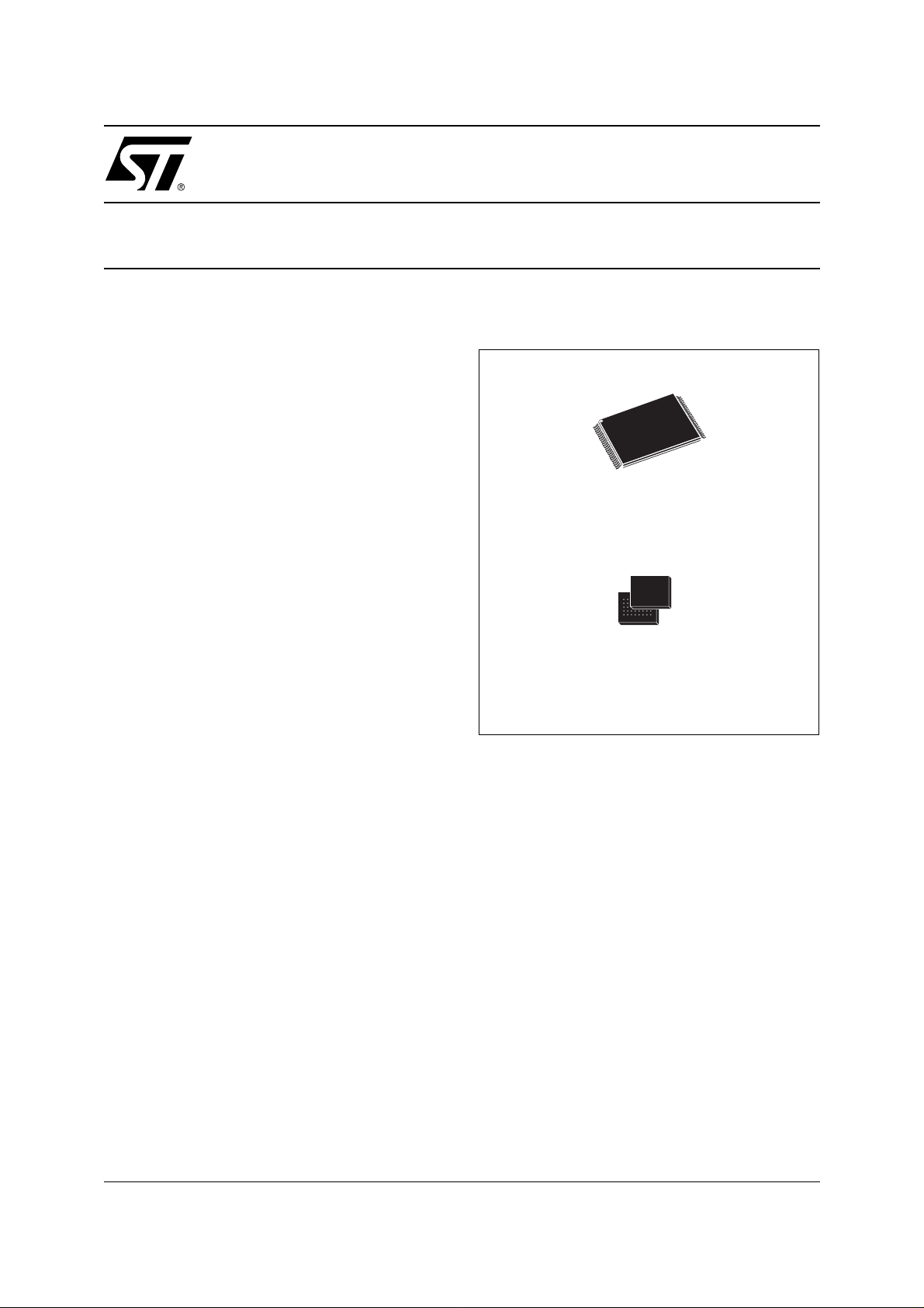
Figure 1. Packages
TSOP48 (N)
12 x 20mm
FBGA
TFBGA48 (ZA)
6 x 9mm
July 2002
This is preliminary information on a new product now in development. Details are subject to change without notice.
1/30
Page 2

M29KW064E
TABLE OF CONTENTS
FEATURES SUMMARY . . . . . . . . . . . . . . . . . . . . . . . . . . . . . . . . . . . . . . . . . . . . . . . . . . . . . . . . . . . . . 1
Figure 1. Packages . . . . . . . . . . . . . . . . . . . . . . . . . . . . . . . . . . . . . . . . . . . . . . . . . . . . . . . . . . . . . . 1
Table 1. Signal Names . . . . . . . . . . . . . . . . . . . . . . . . . . . . . . . . . . . . . . . . . . . . . . . . . . . . . . . . . . . 4
Figure 3. TFBGA Connections (Top view through package). . . . . . . . . . . . . . . . . . . . . . . . . . . . . . . 5
Figure 4. TSOP Connections . . . . . . . . . . . . . . . . . . . . . . . . . . . . . . . . . . . . . . . . . . . . . . . . . . . . . . . 6
Table 2. Block Addresses . . . . . . . . . . . . . . . . . . . . . . . . . . . . . . . . . . . . . . . . . . . . . . . . . . . . . . . . . 6
SIGNAL DESCRIPTIONS . . . . . . . . . . . . . . . . . . . . . . . . . . . . . . . . . . . . . . . . . . . . . . . . . . . . . . . . . . . . 7
Address Inputs (A0-A21). . . . . . . . . . . . . . . . . . . . . . . . . . . . . . . . . . . . . . . . . . . . . . . . . . . . . . . . . . 7
Data Inputs/Outputs (DQ0-DQ7). . . . . . . . . . . . . . . . . . . . . . . . . . . . . . . . . . . . . . . . . . . . . . . . . . . . 7
Data Inputs/Outputs (DQ8-DQ15 ). . . . . . . . . . . . . . . . . . . . . . . . . . . . . . . . . . . . . . . . . . . . . . . . . . .7
Chip Enable (E). . . . . . . . . . . . . . . . . . . . . . . . . . . . . . . . . . . . . . . . . . . . . . . . . . . . . . . . . . . . . . . . . 7
Output Enable (G). . . . . . . . . . . . . . . . . . . . . . . . . . . . . . . . . . . . . . . . . . . . . . . . . . . . . . . . . . . . . . . 7
Write Enable (W). . . . . . . . . . . . . . . . . . . . . . . . . . . . . . . . . . . . . . . . . . . . . . . . . . . . . . . . . . . . . . . .7
Reset (RP). . . . . . . . . . . . . . . . . . . . . . . . . . . . . . . . . . . . . . . . . . . . . . . . . . . . . . . . . . . . . . . . . . . . . 7
Ready/Busy Output (RB). . . . . . . . . . . . . . . . . . . . . . . . . . . . . . . . . . . . . . . . . . . . . . . . . . . . . . . . . . 7
V
Supply Voltage. . . . . . . . . . . . . . . . . . . . . . . . . . . . . . . . . . . . . . . . . . . . . . . . . . . . . . . . . . . . . . 7
CC
V
Program Supply Voltage . . . . . . . . . . . . . . . . . . . . . . . . . . . . . . . . . . . . . . . . . . . . . . . . . . . . . . 7
PP
Vss Ground.. . . . . . . . . . . . . . . . . . . . . . . . . . . . . . . . . . . . . . . . . . . . . . . . . . . . . . . . . . . . . . . . . . . . 7
BUS OPERATIONS. . . . . . . . . . . . . . . . . . . . . . . . . . . . . . . . . . . . . . . . . . . . . . . . . . . . . . . . . . . . . . . . . 8
Bus Read. . . . . . . . . . . . . . . . . . . . . . . . . . . . . . . . . . . . . . . . . . . . . . . . . . . . . . . . . . . . . . . . . . . . . . 8
Bus Write. . . . . . . . . . . . . . . . . . . . . . . . . . . . . . . . . . . . . . . . . . . . . . . . . . . . . . . . . . . . . . . . . . . . . . 8
Output Disable. . . . . . . . . . . . . . . . . . . . . . . . . . . . . . . . . . . . . . . . . . . . . . . . . . . . . . . . . . . . . . . . . . 8
Standby. . . . . . . . . . . . . . . . . . . . . . . . . . . . . . . . . . . . . . . . . . . . . . . . . . . . . . . . . . . . . . . . . . . . . . . 8
Automatic Standby. . . . . . . . . . . . . . . . . . . . . . . . . . . . . . . . . . . . . . . . . . . . . . . . . . . . . . . . . . . . . . . 8
Electronic Signature. . . . . . . . . . . . . . . . . . . . . . . . . . . . . . . . . . . . . . . . . . . . . . . . . . . . . . . . . . . . . . 8
Table 3. Bus Operations . . . . . . . . . . . . . . . . . . . . . . . . . . . . . . . . . . . . . . . . . . . . . . . . . . . . . . . . . . 8
COMMAND INTERFACE . . . . . . . . . . . . . . . . . . . . . . . . . . . . . . . . . . . . . . . . . . . . . . . . . . . . . . . . . . . . 9
Read/Reset Command.. . . . . . . . . . . . . . . . . . . . . . . . . . . . . . . . . . . . . . . . . . . . . . . . . . . . . . . . . . . 9
Auto Select Command. . . . . . . . . . . . . . . . . . . . . . . . . . . . . . . . . . . . . . . . . . . . . . . . . . . . . . . . . . . . 9
Word Program Command.. . . . . . . . . . . . . . . . . . . . . . . . . . . . . . . . . . . . . . . . . . . . . . . . . . . . . . . . . 9
Multiple Word Program Command . . . . . . . . . . . . . . . . . . . . . . . . . . . . . . . . . . . . . . . . . . . . . . . . . .9
Setup Phase . . . . . . . . . . . . . . . . . . . . . . . . . . . . . . . . . . . . . . . . . . . . . . . . . . . . . . . . . . . . . . . . 9
Program Phase. . . . . . . . . . . . . . . . . . . . . . . . . . . . . . . . . . . . . . . . . . . . . . . . . . . . . . . . . . . . . . 9
Verify Phase . . . . . . . . . . . . . . . . . . . . . . . . . . . . . . . . . . . . . . . . . . . . . . . . . . . . . . . . . . . . . . . 10
Exit Phase. . . . . . . . . . . . . . . . . . . . . . . . . . . . . . . . . . . . . . . . . . . . . . . . . . . . . . . . . . . . . . . . . 10
Block Erase Command.. . . . . . . . . . . . . . . . . . . . . . . . . . . . . . . . . . . . . . . . . . . . . . . . . . . . . . . . . . 10
Chip Erase Command. . . . . . . . . . . . . . . . . . . . . . . . . . . . . . . . . . . . . . . . . . . . . . . . . . . . . . . . . . . 10
Table 4. Standard Commands. . . . . . . . . . . . . . . . . . . . . . . . . . . . . . . . . . . . . . . . . . . . . . . . . . . . . 11
Table 5. Multiple Word Program Command . . . . . . . . . . . . . . . . . . . . . . . . . . . . . . . . . . . . . . . . . . 11
Table 6. Program, Erase Times and Program, Erase Endurance Cycles . . . . . . . . . . . . . . . . . . . . 11
Table 7. Multiple Word Program Timings . . . . . . . . . . . . . . . . . . . . . . . . . . . . . . . . . . . . . . . . . . . . 11
2/30
Page 3

M29KW064E
Figure 5. Multiple Word Program Flowchart . . . . . . . . . . . . . . . . . . . . . . . . . . . . . . . . . . . . . . . . . . 12
STATUS REGISTER. . . . . . . . . . . . . . . . . . . . . . . . . . . . . . . . . . . . . . . . . . . . . . . . . . . . . . . . . . . . . . . 13
Data Polling Bit (DQ7). . . . . . . . . . . . . . . . . . . . . . . . . . . . . . . . . . . . . . . . . . . . . . . . . . . . . . . . . . . 13
Toggle Bit (DQ6).. . . . . . . . . . . . . . . . . . . . . . . . . . . . . . . . . . . . . . . . . . . . . . . . . . . . . . . . . . . . . . . 13
Error Bit (DQ5). . . . . . . . . . . . . . . . . . . . . . . . . . . . . . . . . . . . . . . . . . . . . . . . . . . . . . . . . . . . . . . . . 13
VPP Status Bit (DQ4) . . . . . . . . . . . . . . . . . . . . . . . . . . . . . . . . . . . . . . . . . . . . . . . . . . . . . . . . . . . 13
Erase Timer Bit (DQ3). . . . . . . . . . . . . . . . . . . . . . . . . . . . . . . . . . . . . . . . . . . . . . . . . . . . . . . . . . . 13
Alternative Toggle Bit (DQ2).. . . . . . . . . . . . . . . . . . . . . . . . . . . . . . . . . . . . . . . . . . . . . . . . . . . . . . 13
Multiple Word Program Bit (DQ0) . . . . . . . . . . . . . . . . . . . . . . . . . . . . . . . . . . . . . . . . . . . . . . . . . . 13
Table 8. Status Register Bits. . . . . . . . . . . . . . . . . . . . . . . . . . . . . . . . . . . . . . . . . . . . . . . . . . . . . . 14
Figure 6. Data Polling Flowchart . . . . . . . . . . . . . . . . . . . . . . . . . . . . . . . . . . . . . . . . . . . . . . . . . . . 14
Figure 7. Data Toggle Flowchart. . . . . . . . . . . . . . . . . . . . . . . . . . . . . . . . . . . . . . . . . . . . . . . . . . . 14
MAXIMUM RATING. . . . . . . . . . . . . . . . . . . . . . . . . . . . . . . . . . . . . . . . . . . . . . . . . . . . . . . . . . . . . . . . 15
Table 9. Absolute Maximum Ratings. . . . . . . . . . . . . . . . . . . . . . . . . . . . . . . . . . . . . . . . . . . . . . . .15
DC and AC PARAMETERS . . . . . . . . . . . . . . . . . . . . . . . . . . . . . . . . . . . . . . . . . . . . . . . . . . . . . . . . . 16
Table 10. Operating and AC Measurement Conditions. . . . . . . . . . . . . . . . . . . . . . . . . . . . . . . . . . 16
Figure 8. AC Measurement I/O Waveform . . . . . . . . . . . . . . . . . . . . . . . . . . . . . . . . . . . . . . . . . . . 16
Figure 9. AC Measurement Load Circuit . . . . . . . . . . . . . . . . . . . . . . . . . . . . . . . . . . . . . . . . . . . . . 16
Table 11. Device Capacitance . . . . . . . . . . . . . . . . . . . . . . . . . . . . . . . . . . . . . . . . . . . . . . . . . . . . . 1 6
Table 12. DC Characteristics. . . . . . . . . . . . . . . . . . . . . . . . . . . . . . . . . . . . . . . . . . . . . . . . . . . . . . 17
Figure 10. Read AC Waveforms . . . . . . . . . . . . . . . . . . . . . . . . . . . . . . . . . . . . . . . . . . . . . . . . . . . 18
Table 13. Read AC Characteristics . . . . . . . . . . . . . . . . . . . . . . . . . . . . . . . . . . . . . . . . . . . . . . . . . 1 8
Figure 11. Write AC Waveforms, Write Enable Controlled . . . . . . . . . . . . . . . . . . . . . . . . . . . . . . . 19
Table 14. Write AC Characteristics, Write Enable Controlled . . . . . . . . . . . . . . . . . . . . . . . . . . . . . 20
Figure 12. Write AC Waveforms, Chip Enable Controlled . . . . . . . . . . . . . . . . . . . . . . . . . . . . . . . . 21
Table 15. Write AC Characteristics, Chip Enable Controlled . . . . . . . . . . . . . . . . . . . . . . . . . . . . . 22
Figure 13. Reset AC Waveforms . . . . . . . . . . . . . . . . . . . . . . . . . . . . . . . . . . . . . . . . . . . . . . . . . . . 23
Table 16. Reset AC Characteristics . . . . . . . . . . . . . . . . . . . . . . . . . . . . . . . . . . . . . . . . . . . . . . . . 23
PACKAGE MECHANICAL . . . . . . . . . . . . . . . . . . . . . . . . . . . . . . . . . . . . . . . . . . . . . . . . . . . . . . . . . . 24
Figure 14. TSOP48 - 48 lead Plastic Thin Small Outline, 12 x 20mm, Package Outline . . . . . . . . 24
Table 17. TSOP48 - 48 lead Plastic Thin Small Outline, 12 x 20mm, Package Mechanical Data . 24
Figure 15. TFBGA48 6x9mm - 8x6 ball array, 0.80 mm pitch, Bottom View Package Out line . . . . 25
Table 18. TFBGA48 6x9mm - 8x6 ball array, 0.80 mm pitch, Package Mechanical Data. . . . . . . . 25
Figure 16. TFBGA48 Daisy Chain - Package Connections (Top view through package) . . . . . . . . 26
Figure 17. TFBGA48 Daisy Chain - PCB Connections (Top view through package) . . . . . . . . . . . 27
PART NUMBERING . . . . . . . . . . . . . . . . . . . . . . . . . . . . . . . . . . . . . . . . . . . . . . . . . . . . . . . . . . . . . . . 28
Table 19. Ordering Information Scheme . . . . . . . . . . . . . . . . . . . . . . . . . . . . . . . . . . . . . . . . . . . . . 28
Table 20. Daisy Chain Ordering Scheme . . . . . . . . . . . . . . . . . . . . . . . . . . . . . . . . . . . . . . . . . . . . 28
REVISION HISTORY. . . . . . . . . . . . . . . . . . . . . . . . . . . . . . . . . . . . . . . . . . . . . . . . . . . . . . . . . . . . . . . 29
Table 21. Document Revision History . . . . . . . . . . . . . . . . . . . . . . . . . . . . . . . . . . . . . . . . . . . . . . .29
3/30
Page 4
M29KW064E
SUMMARY DESCRIPTION
The M29KW064E LightFlash™ is a 64 M bit ( 4Mb
x16) non-volatile memory that can be read, erased
and reprogrammed. Read op erations can b e performed using a single low voltage (2.7 to 3.6V)
supply. Program an d Er ase operations require an
additional V
power-up the memory defaults to its Read mode
where it can be read in the same way as a ROM or
EPROM.
The memory is divided into 32 uniform blocks that
can be erased i ndependently so it is poss ible to
preserve valid data whi le old data is erased (see
Figures 2, Block Address es). Program a nd Erase
commands are written to the Command Interface
of the memory. An on-chip Program/Erase Controller (P/E.C.) simplifies the process of programming or erasing the memory by taking care of all of
the special operations that are required to update
the memory contents.
(11.4 to 12.6) power supply. On
PP
The M29KW064E LightFlash™ features a new
command, Multiple Word Program, used to program large streams of dat a. I t gre atly reduc es t he
total programming time when a large number of
Words are written to the memory at any one time.
Using this command the entire memory can be
programmed in 8s, compared to 36s using the
standard Word Program.
The end of a program or erase operation can be
detected and any error conditions identified. The
command set required to control the memory is
consistent with JEDEC standards.
Chip Enable, Output Enable and Write Enable signals control the bus operation of the memory.
They allow simple conne ction to most m icroprocessors, often without additional logic.
The memory is offered in TSOP48 (12 x 20mm)
and TFBGA48 (6 x 9mm, 0.8mm pitch) packages.
The memory is supplied with all the bits erased
(set to ’1’).
Figure 2. Logic Diagram Table 1. Signal Names
A0-A21 Address Inputs
V
V
22
A0-A21 DQ0-DQ15
W
E
G
RP
M29KW064E
V
CC
SS
PP
16
RB
AI06264
DQ0-DQ15 Data Inputs/Outputs
E
G
W
RP
RB
V
CC
V
PP
V
SS
NC Not Connected Internally
Chip Enable
Output Enable
Write Enable
Reset
Ready/Busy Output
Supply Voltage read
Supply Voltage program erase
Ground
4/30
Page 5
Figure 3. TFBGA Connections (Top view through package)
M29KW064E
654321
A
B
C
D
E
F
G
H
A3
A4
A2
A1
A0
E
G
V
SS
A7
A17
A6
A5
DQ0
DQ8
DQ9
DQ1
RB
V
PP
A18
A20
DQ2
DQ10
DQ11
DQ3
W
RP
A21
A19
DQ5
DQ12
V
CC
DQ4
A9
A8
A10
A11
DQ7
DQ14
DQ13
DQ6
A13
A12
A14
A15
A16
NC
DQ15
V
SS
AI06265
5/30
Page 6
M29KW064E
Figure 4. TSOP Connections Table 2. Block Addresses
Block Number Address Range
32 3E0000h-3FFFFFh
A15
1
A14
A13
A12
A11
A10 DQ14
A9
A8
A19
A20
W
RP
A21
V
PP
12
M29KW064E
13
RB
A18
A17
A7
A6
A5
A4
A3
A2
A1
24 25
48
37
36
A16
NC
V
SS
DQ15
DQ7
DQ6
DQ13
DQ5
DQ12
DQ4
V
CC
DQ11
DQ3
DQ10
DQ2
DQ9
DQ1
DQ8
DQ0
G
V
SS
E
A0
31 3C0000h-3DFFFFh
30 3A0000h-3BFFFFh
29 380000h-39FFFFh
28 360000h-37FFFFh
27 340000h-35FFFFh
26 320000h-33FFFFh
25 300000h-31FFFFh
24 2E0000h-2FFFFFh
23 2C0000h-2DFFFFh
22 2A0000h-2BFFFFh
21 280000h-29FFFFh
20 260000h-27FFFFh
19 240000h-25FFFFh
18 220000h-23FFFFh
17 200000h-21FFFFh
16 1E0000h-1FFFFFh
15 1C0000h-1DFFFFh
14 1A0000h-1BFFFFh
13 180000h-19FFFFh
6/30
AI06266
12 160000h-17FFFFh
11 140000h-15FFFFh
10 120000h-13FFFFh
9 100000h-11FFFFh
8 0E0000h-0FFFFFh
7 0C0000h-0DFFFFh
6 0A0000h-0BFFFFh
5 080000h-09FFFFh
4 060000h-07FFFFh
3 040000h-05FFFFh
2 020000h-03FFFFh
1 000000h-01FFFFh
Page 7

SIGNAL DESCRIPTIONS
See Figure 2, Logic Diagram, and Table 1, Sign al
Names, for a brief overview of the signals connected to this device.
Address Inputs (A0-A21). The Address Inputs
select the cells i n the memory array to a ccess during Bus Read operations. During Bus Write operations they control the commands sent to the
Command Interface of the Program/Erase Controller.
Data Inputs/Outputs (DQ0-DQ7). The Data Inputs/Outputs outputs the data stored at the selected address during a Bus Rea d operation. Du ring
Bus Write operations they represent the commands sent to the Command Interface of the Program/Erase Controller.
Data Inputs/Outputs (DQ8-DQ15). The Data Inputs/Outputs output the data stored at the selected
address during a Bus Read operation. During Bus
Write operations the Command Register does not
use these bits. When reading t he Status Register
these bits should be ignored.
Chip Enable (E
). The Chip Enable, E, activates
the memory, allowing Bus Read and Bus Write operations to be performed. When Chip Enable is
High, V
Output Enable (G
, all other pins are ignored.
IH
). The Output Enable, G, con-
trols the Bus Read operation of the memory.
Write Enable (W
). The Write Enable, W, controls
the Bus Write operation of the memory’s Command Interf a c e .
Reset (RP
). The Reset pin can be used to apply
a Hardware Reset to the memory.
A Hardware Reset is achieved by holding Reset
Low, V
V
IH
Bus Write operations after t
, fo r at least t
IL
. After Reset goes High,
PLPX
, the memory will be ready for B us Read and
PHEL
or t
RHEL
, which ever occurs last. See the Ready/Busy Output section, Table 16 and Figure 13, Reset AC
Characteristics for more details.
Ready/Busy Output (RB
). The Ready/Busy pin
is an open-drain output that can be used to identify
when the memory array can be read. Ready/Busy
is high-impedance during Read mode and Auto
Select mode. After a Hardware Reset, Bus Read
and Bus Write operations cannot begin until
M29KW064E
Ready/Busy becomes high-impedance. See Table
16 and Figure 13, Reset AC Characteristics.
During Program or Erase operations Ready/Busy
is Low, V
Read/Reset commands or Hardw are Resets until
the memory is ready to enter Read mode.
The use of an open-drain output allows the Ready/
Busy pins from several memories to be connected
to a single pull-up resistor. A Low will then indicate
that one, or more, of the memories is busy.
Supply Voltage. The VCC Supply Voltage
V
CC
supplies the power for Read operations.
The Command Interface is disabled when the V
Supply Voltage is less than the L ockout Voltage,
V
. This prevents Bus Write operations from ac-
LKO
cidentally damaging the data during power up,
power down and power surges. If the Program/
Erase Controller is programming or erasing during
this time then the operation aborts and the memory contents being altered will be invalid.
A 0.1µF capacitor should be connected between
the V
pin to decouple the current surges from the power
supply. The PCB track widths must be sufficient to
carry the currents required during program and
erase operations, I
Program Supply Voltage. VPP is both a
V
PP
power supply and Write Protect pin. The two functions are selected by t he voltage range a pplied t o
the pin. The Supply Voltage V
before the Program Supply Voltage V
If V
PP
power supply pin for program and erase operations. V
algorithm is completed.
If V
PP
V
is seen as a Write Protect pin. In this case a
PP
voltage lower than V
tion against program or erase, while V
range of V
12, DC Characteristics for the relevant values).
Note that V
nected as the device may become unreliable.
Vss Ground. The V
for all voltage measurements.
. Ready/Busy will remain Low during
OL
Supply Voltage pin and the VSS Ground
CC
.
CC3
must be applied
CC
PP
.
is in the range 11.4V to 12.6V it acts as a
must be stable until the Program/Erase
PP
is kept in a low voltage range (0V to 3.6V)
gives an absolute p rotec-
HH
enables these functions (see Ta ble
HH
must not be left floating o r uncon-
PP
Ground is the reference
SS
in the
PP
CC
7/30
Page 8
M29KW064E
BUS OPERATIONS
There are six standard bus operations that control
the device. These are Bus Read, Bus Wri te, Output Disable, Standby, Automatic Standby and
Electronic Signature. See Tables 3, Bus Operations, for a summary. Typically glitches of less
than 5ns on Chip Enable or Write Enable are ignored by the memory and do not affect bus operations.
Bus Read. Bus Read operations read from the
memory cells, or specific registers in the Command Interface. A valid Bus Read operation involves setting the desired address on the Address
Inputs, applying a Low sig nal, V
and Output Enable and keeping Write Enable
High, V
. The Data Inputs/Outputs will output the
IH
value, see Figure 10, Read Mode AC Waveforms,
and Table 13, Read AC Characteristics, for details
of when the output becomes valid.
Bus Write. Bus Write operations write to the
Command Interface. A valid Bus Write operation
begins by setting the desire d address on t he Address Inputs. The Address Inputs are latched by
the Command Interface on the falling edge of Chip
Enable or Write Enable, whichever occurs last.
The Data Inputs/Outputs a re latched by the Command Interface on the rising edge of Chip Enable
or Write Enable, whichever occurs first. Output Enable must remain High, V
IH
Write operation. See Figures 11 and 12, Write AC
Waveforms, and Tables 14 and 15, Write AC
, to Chip Enable
IL
, during the whole Bus
Characteristics, for details of the timing requirements.
Output Disa bl e . The Data Inputs/Outputs are in
the high impedance s tate when Output Enable is
High, V
Standby. When Chip Enable is High, V
.
IH
, the
IH
memory enters Standby mode and the Data Inputs/Outputs pins are placed in the high-impedance state. To reduce the S upply Current to the
Standby Supply Current, I
be held within V
± 0.2V. For the Standby current
CC
, Chip Enable should
CC2
level see Table 12, DC Characteristics.
During program or erase operations the memory
will continue to use the Program/Erase Supply
Current, I
, for Program or Erase operations un-
CC3
til the operation completes.
Automatic Standby. If CMOS levels (V
± 0.2V)
CC
are used to drive the bus and the bus is inactive for
150ns or more the memory enters Automatic
Standby where the internal Supply Current is reduced to the Standby Supply Current, I
CC2
. The
Data Inputs/Outputs will still output data if a Bus
Read operation is in progress.
Electronic Signature. The memory has two
codes, the manufacturer code and the device
code, that can be read to identify the memory.
These codes can be read by applying t he signals
listed in Tables 3, Bus Operations.
Table 3. Bus Operations
V
V
XX
PP
HH
X
XX
XX
Operation E G W
V
IL
V
IH
V
IH
X X X X Hi-Z
V
IL
V
IL
or V
HH
V
IL
V
IL
V
IH
V
IL
V
IL
Bus Read
Bus Write
Output Disable X
Standby
Read Manufacturer
Code
Read Device Code
Note: 1. X = VIL or VIH.
2. XX = V
3. Not necessary for A uto Select or Read/Res et command s.
4. When re adi ng the Status Register during Program or Eras e operations, V
, V
IL
IH
V
IH
V
IL
V
IH
V
IH
V
IH
Address Inputs
A0-A21
(4)
Cell Address Data Output
(3)
Command Address Data Input
X Hi-Z
A0 = V
Others V
A0 = V
Others V
, A1 = VIL,
IL
or V
IL
IH
, A1 = VIL,
IH
or V
IL
IH
must be kept at VHH.
PP
Data Inputs/Outputs
DQ15-DQ0
0020h
88AFh
8/30
Page 9

COMMAND INTERFACE
All Bus Write operations t o the me mory are in terpreted by the Command Interface. Commands
consist of one or more sequential Bus Write operations. Failure to observe a valid sequence of Bus
Write operations will result in the memory returning to Read mode. The long command sequences
are imposed to maximize data security.
Refer to Tables 4 and 5, for a summary of the commands.
Read/Reset Command.
The Read/Reset command returns the memory to
its Read mode where it behaves like a ROM or
EPROM, unless otherwise stated. It also resets
the errors in the Status Register. Either one or
three Bus Write operations can be u sed to issue
the Read/Reset command.
The Read/Reset Command can be issued, between Bus Write cycles before the start of a program or erase operation, to return the device to
read mode. Once the program or erase operation
has started the Read/Reset command is no longer
accepted. The Read/Res et co mmand is executed
regardless of the value of V
(VIL, VIH or VHH).
PP
Auto Select Command.
The Auto Select command is used to read the
Manufacturer Code and the Device Code. Three
consecutive Bus Write operations are re quired to
issue the Auto Selec t command. Onc e the Auto
Select command is issued the memory remains in
Auto Select mode until a Read/Reset command is
issued, all other commands are ignored. The Auto
Select command is executed regardless of the value of V
(VIL, VIH or VHH).
PP
From the Auto Select mode the Manufacturer
Code can be read using a Bus Read operation
with A0 = V
may be set to either V
and A1 = VIL. The other address bits
IL
or VIH.
IL
The Device Code can be read using a B us Read
operation with A0 = V
address bits may be set to either V
and A1 = VIL. The other
IH
or VIH.
IL
Word Progr a m Com m a n d.
The Word Program command can be used to program a Word to the memory array. V
set to V
ther V
during Word Program. If VPP is set to ei-
HH
or VIH the command will be ignored, the
IL
must be
PP
data will remain unchanged and the device will revert to Read/Reset mode. The command requires
four Bus Write operations, the final write operation
latches the address and data in the internal state
machine and starts the Program/Erase Controller.
During the program operat ion the memo ry will ignore all commands. I t is n ot poss ible t o iss ue any
command to abort or pause the operation. Typical
program times are given in Table 6. Bus Read operations during the program o peration will output
M29KW064E
the Status Register on the Data Inputs/Outputs.
See the section on the S tatus Register for more
details.
After the program operation has completed the
memory will return to the Read mode, unle ss an
error has occurred. When an error occurs the
memory will continue to output the Status Register. A Read/Reset command must be issued to reset the error condition and return to Read mode.
Note that the Program command cannot change a
bit set at ’0’ bac k to ’1’. One of the E rase Commands must be used to set all the bits in a block or
in the whole memory from ’0’ to ’1’.
Multiple Word Program Command
The Multiple Word Program command can be
used to program large streams of data. It greatly
reduces the total programming time when a l arge
number of Words are written to the memory at any
one time. V
Word Progr am. If V
command will be ignored, the data will remain unchanged and the device will revert to Read/Reset
mode.
It has four phases: the Setup P hase to initiate the
command, the Program Phase to program the
data to the memory, the Verify Phase to check that
the data has been correctly programmed and reprogram if necessary and the Exit Phase.
Setup Phase. The M ultiple Word Program command requires three Bus Write operations to initiate the command (refer to Table 5, Multiple Word
Program Command and Figure 5, Multiple Word
Program Flowchart). The Status Register Toggle
bit (DQ6) should be checked to verify that the operation has started and the Multiple Word Program
bit (DQ0) checked to verify that the P/E.C. is ready
for the first Word.
Program Phase. The Program Phase requires
n+1 cycles, where n is the number of Words, to execute the programming phase (refer to Table 5,
Multiple Word Program Command and Figure 5,
Multiple Word Program Flowchart).
Three successive steps are required to issue and
execute the Program Phase of the command.
1. The fourth Bus Write operation of the command
latches the Start Address and the first Word to
be programmed. The Status Register Multiple
Word Program bit (DQ0) should be read to
check that the P/E.C. is ready for the next Word.
2. Each subsequent Word to be programmed is
latched with a new Bus Write operation. The
address can remain the Start Address, be
incremented or be any address in the same
block, as the device automatically increments
the address with each sucssesive Bus Write
must be set to VHH during Multiple
PP
is set to e ither V
PP
or VIH the
IL
9/30
Page 10

M29KW064E
cycle. If the command is used to program in
more than one block then the address must
remain in the starting block as any address that
is not in the same block as the Start Address
terminates the Program operation. The Status
Register Multiple Word Program bit (DQ0) must
be read between each Bus Write cycle to check
that the P/E.C. is ready for the next Word.
3. Finally, after all Words have been programmed,
write one Bus Write operat ion to any address
outside the block containing the Sta rt Address,
to terminate the programming phase.
The memory is now set to enter the Verify Phase.
Verify Phase. Th e Verify Phase is s imilar to the
Program Phase in that all Words must be resent to
the memory for them to be che cked against the
programmed data. If the ch eck fails the P /E.C wi ll
try to reprogram the correct data. The P/E.C will
remain busy until the correct data has been successfully programmed. The Verify Phase is mandatory. If the Verify Phase is not executed the
programmed data cannot be guaranteed.
Three successive steps are required to execute
the Verify Phase of the command.
1. Use one Bus Write operation to latch the Start
Address and the first Word, to be verified. The
Status Register Multiple Word Program bit
(DQ0) should be read to check that the P/E.C. is
ready for the next Word.
2. Each subsequent Word to be verified is latched
with a new Bus Write operation. If any address
that is not in the same block as the Start
Address is given, the Verify operation
terminates. The Status Register Multiple Word
Program (DQ0) must be read to check that the
P/E.C. is ready for the next Word.
3. Finally, after all Words have been verified, write
one Bus Write operation to any address outside
the block containing the Start Address, to
terminate the Verify Phase.
Exit Phase . Read the Status Register to verify
that DQ6 has stopped toggling. If the Verify Phase
is successfully completed the memory returns to
the Read mode. If the P/E.C. fails to reprogram a
given location, the Verify Phase will terminate and
Error bit DQ5 will be set in the Status Register. If
the error is due to a V
failure DQ4 w ill als o be
PP
set. If the operation fails a Read/ Reset com mand
must be issued to return the device to Read mode.
It is not possible to issue any c ommand to abort or
pause the operation. Typical program times are
given in Table 6. Bus Read operations du ring the
program operatio n will outpu t the Sta tus Regi ster
on the Data Inputs/Outputs. See the section on the
Status Register for more details.
Note that the Multiple Word Program command
cannot change a bit set at ’0’ back to ’1’. One of the
Erase Commands must be used to set all the bits
in a block or in the whole memory from ’0’ to ’1’.
Block Erase Command.
The Block Erase com mand can be used to erase
a block. It sets all of the bits in the block to ’1’. All
previous data in the block is lost.
must be set to VHH during Block Erase. If V
V
PP
is set to either V
or VIH the command will be ig-
IL
PP
nored, the data will remain unchanged and the device will revert to Read/Reset mode.
Six Bus Write operations are required to select the
block . The Block Erase operation starts the Program/Erase Controller after the last Bus Write operation. The Status Register can be read after the
sixth Bus Write operation. See the Status Register
for details on how to identify if the P rogram /Erase
Controller has started the Block Erase operation.
During the Block Erase operation the me mory wi ll
ignore all commands. Typical block erase times
are given in Table 6. All Bus Read operations during the Block Erase operation will output the Status Register on the Data Inputs/Outputs. See the
section on the Status Register for more details.
After the Block Erase operation has completed the
memory will return to the Read Mode, unle ss an
error has occurred. When an error occurs the
memory will continue to output the Status Register. A Read/Reset command must be issued to reset the error condition and return to Read mode.
Chip Erase Command.
The Chip Erase command can be used to erase
the entire memory. It sets all of the bits in the memory to ’1’. All previous data in the memory is lost.
must be set to VHH during Chip Erase. If V
V
PP
is set to either V
or VIH the command will be ig-
IL
PP
nored, the data will remain unchanged and the device will revert to Read/Reset mode. Six Bus Write
operations are required to issue the Chip Erase
Command and start the Program/Erase Controller.
During the erase operation the memory will ignore
all commands. It is not possible to issue any command to abort the operation. Typical chip erase
times are given in Table 6. All Bus Read operations during the Chip E rase operation will output
the Status Register on the Data Inputs/Outputs.
See the section on the S tatus Register for more
details.
After the Chip Erase operation has completed t he
memory will return to the Read Mode, unle ss an
error has occurred. When an error occurs the
memory will continue to output the Status Register. A Read/Reset command must be issued to reset the error condition and return to Read Mode.
10/30
Page 11

M29KW064E
Table 4. Standard Commands
Bus Write Operations
Command
Length
1X F0
Read/Reset
3 555 AA 2AA 55 X F0
Auto Select 3 555 AA 2AA 55 555 90
Word Program 4 555 AA 2AA 55 555 A0 PA PD
Block Erase 6 555 AA 2AA 55 555 80 555 AA 2AA 55 BA 30
Chip Erase 6 555 AA 2AA 55 555 80 555 AA 2AA 55 555 10
Note: X Don’t Care, PA Program Address, PD Program Data, BA A ny addres s in the B lo ck . All values in the t able are in hexadecim al . The
Comma nd I n t erface only uses A0-A10 and DQ0-DQ7 to verif y t he commands; A11-A21, DQ8-DQ15 are Don’t Care.
Table 5. Multiple Word Program Command
Phase
Length
Add Data Add Data Add Data Add Data A dd Data Add Data Add Data
Program
Verify n+1 PA1 PD1 PA1 PD2 PA1 PD3 PA1 PD4 PA1 PD5 PA1 PAn
Note: A Bus Read must be done between each Write cycle where the data is programmed or verified, to Read the Status Register and check
3+n
555 AA 2AA 55 555 20
+1
that the memo ry is r eady t o ac ce pt th e next dat a. NO T P A1 i s any ad dress that is not in t he s ame b loc k a s PA1. X D on’t Care , n =
number of Words to be programmed.
1st 2nd 3rd 4th 5th 6th
Add Data Add Data Add Data Add Data Add Data Add Data
Bus Write Operations
1st 2nd 3rd 4 th 5th Final -1 F inal
PD1 PA1 PD2 PA1 PAn
PA1
NOT
PA1
NOT
PA1
X
X
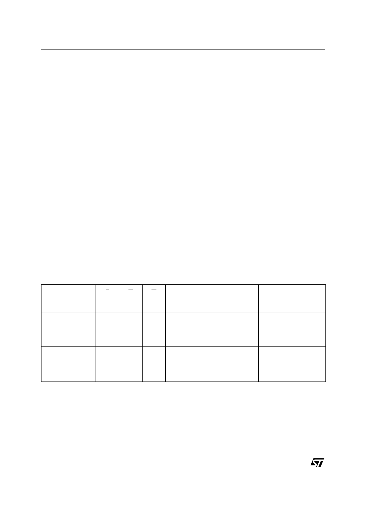
Table 6. Program, Erase Times and Progra m, Erase Endu ran ce Cycle s
Parameter Min
Typ
(1)
Chip Erase 41 44 120 s
Block Erase (128 KWords) 1.5 6 s
Program (Word) 9 250 µs
Chip Program (Multiple Word) 8 144 s
Chip Program (Word by Word) 36 144 s
Program/Erase Cycles (per Block) 10,000 cycles
Note: 1. TA = 25°C, VPP = 12V.
Typical after
10k W/E Cycles
(1)
Max Unit
Table 7. Multiple Word Program Timings
Symbol Parameter Min Typ Max Unit
t
MWP-SETUP
t
MWP-PROG
t
MWP-TRAN
t
MWP-END
Note: 1. MWP = Multiple Word Program.
MWP Setup time 500 ns
MWP Program Time 9 250 µs
MWP Program to Verify transition 2 10 20 µs
MWP Verify to End transition 2 3 µs
11/30
Page 12

M29KW064E
Figure 5. Mul ti pl e W or d Program Fl owchart
Setup
Phase
NO
Setup time
exceeded?
YES
EXIT (
Program
Phase
(t
MWP-SETUP
setup failed)
Start
Write AAh
Address 555h
Write 55h
Address 2AAh
Write 20h
Address 555h
Read Status
Register
NO
DQ6
toggling?
(1)
)
YES
NO
DQ0 = 0?
YES
Write Data1(PD
Start Address (PA1)
Read Status
Register
DQ0 = 0?
Write Data 2 (PD2)
Address in Start Block
Read Status
Register
DQ0 = 0?
Write Data n (PDn)
Address in Start Block
YES
YES
)
1
NO
NO
Read Status
Register
(t
MWP-TRAN
DQ0 = 0?
YES
Write Data1 (PD1)
Start Address (PA1)
Read Status
Register
DQ0 = 0?
YES
Write Data 2 (PD2)
Address in Start Block
Read Status
Register
DQ0 = 0?
YES
Write Data n (PDn)
Address in Start Block
Read Status
Register
DQ0 = 0?
Write XX
Any Address
NOT in Start Block
Read Status
Register
NO
YES
NO
NO
NO
(1)
)
program time
exceeded?
(t
MWP-PROG
program time
exceeded?
(t
MWP-PROG
program time
exceeded?
(t
MWP-PROG
Word
Word
Word
Verify
Phase
NO
NO
(1)
NO
YES
YES
(1)
)
YES
)
YES
(1)
)
Read Status
Register
DQ5 = 1
DQ4 = 0?
NO
Exit
Phase
Read Status
Register
toggling?
DQ0 = 0?
YES
Write XX
Any Address
NOT in Start Block
NO
Note: 1. Ref er to Table 7, M ul tiple Word Program Ti mings, for the values.
12/30
DQ6
NO
(t
YES
(1)
MWP-END
)
Exit (read mode)
Fail error
Write F0h
Address XX
Fail, VPP error
AI05554c
Page 13

STATUS REGISTER
Bus Read operations from any address always
read the Status Register during Program and
Erase operations. The bi ts in the Status Register
are summarized in Table 8, Status Register Bits.
Data Polling Bit (DQ7). The Data Polling Bit can
be used to identify whether the Program/Erase
Controller has successfully completed its operation. The Data Polling Bit is output on DQ7 when
the Status Register is read.
During a Word Program operation the Data Polling
Bit outputs the complement of the bit being programmed to DQ7. After successful completion of
the Word Program ope ration the memory ret urns
to Read mode and Bus Read operations from the
address just programmed output DQ7, not its complement. The Data P olling Bit is not av ailable during a Multiple Word Program operation.
During Er ase ope rations the Data Polling Bit ou t-
puts ’0’, the complement of the erased state of
DQ7. After successful completion of the Erase operation the memory returns to Read Mode.
Figure 6, Data Polling Flowchart, gives an example of how to use the Data Polling Bit. A Valid Address is the address being programmed or an
address within the block being erased.
Toggle Bit (DQ6). The Toggle Bit can be used to
identify whether the Program/Erase Controller has
successfully completed its operation. The Toggle
Bit is output on DQ6 wh en the Status Register is
read.
During Program and Erase operations the Toggle
Bit changes from ’0’ to ’ 1’ to ’ 0’, et c., with su ccessive Bus Read operations at any address. After
successful completion of the operation the memory returns to Read mode.
Figure 7, Data Toggle Flowcha rt, gives an example of how to use the Data Toggle Bit.
Error Bit (DQ5). The Error Bit can be used to
identify errors detected by the Program/Erase
Controller. The Error B it is set to ’1’ when a Program, Block Erase or Chip Erase operation fails to
write the correct data to the memory. If the Error
Bit is set a Read/Rese t command must be iss ued
M29KW064E
before other commands are issued. The E rror bit
is output on DQ5 when the Status Register is read.
Note that the Program command cannot change a
bit set to ’0’ back to ’1’ and attempting to do so will
set DQ5 to ‘1’. A Bus Read operation to that address will s h ow the bit is s ti ll ‘0’. One o f t he E r as e
commands must b e used to set all the bits in a
block or in the whole memory from ’0’ to ’1’.
Status Bit (DQ4). The VPP Status Bit can be
V
PP
used to identify if any Program or Erase operation
has failed due to a V
during any Program or Erase operation, the operation aborts and DQ4 is set to ‘1’. If V
V
throughout the Program or Erase operat ion,
HH
the operation completes and DQ4 is set to ‘0’.
Erase Timer Bit (DQ3). The Erase Timer Bit can
be used to identify the start of Program/Erase
Controller operation during a Block Erase command. Once the Program/Erase Controller starts
erasing the Erase Timer Bit is set t o ’ 1’. The Erase
Timer Bit is output on DQ3 when the Status Register is read .
Alternative Toggle Bit (DQ2). The Alternative
Toggle Bit can be used to monitor the Program/
Erase controller during Block and Chip Erase operations. The Alternative Toggle Bit is out put on
DQ2 when the Status Register is read.
During Erase operations the Toggle Bit changes
from ’0’ to ’1’ to ’0 ’, etc. , wit h su ccessive Bu s Read
operations to any address. Once the operation
completes the memory returns to Read mode.
If an Erase operation f ails a nd the Error Bit is set,
the Alternative Toggle Bit will continue to toggle
with successive Bus Read operations to any address. The Alternative Toggle Bit does not change
if the addressed block has erased correctly.
Multiple Word Program Bit (DQ0). The Multiple
Word Program Bit can be used to indicate whether
the Program/Erase Controller is a ctive or inactive
during Multiple Word Program. When the Program/Erase Controller has written one Word and is
ready to accept the next Word, the bit is set to ‘0’.
Status Register Bit DQ1 is reserved.
error. If V
PP
falls below V
PP
remains at
PP
HH
13/30
Page 14

M29KW064E
Table 8. Status Register Bits
Operation Condition DQ7 DQ6 DQ5 DQ4 DQ3 DQ2 DQ0 RB
Word Program Any Address DQ7 Toggle 0 –– – –0
V
Word Program
Error
Block/ Chip
Erase
Erase Error
Multiple Word
Program
= V
PP
HH
< V
V
PP
HH
Any Address 0 Toggle 0 – 1
V
= V
PP
HH
V
< V
PP
HH
P/E.C. active – Toggle 0 – – – 1 0
P/E.C. inactive,
waiting for next
Word
DQ7 Toggle 1 0 – – – 0
DQ7 Toggle 1 1 – – – 0
0 Toggle 1 0 1
0 Toggle 1 1 1
Toggle
Toggle
Toggle
(2)
(2)
(2)
–0
–0
–0
– Toggle 0 – – – 0 1
Multiple Word
V
PP
= V
HH
– Toggle 1 0 – – 1 0
Program
V
Error
Note: 1. Unspecified dat a bi ts should be ignored.
2. DQ2 toggl es on any addr ess during Block or Chip E rase and after an Erase error.
PP
< V
HH
– Toggle 1 1 – – 1 0
Figure 6. Dat a Po ll i ng Fl o wc h a rt Figure 7. Data To ggl e Fl owchart
READ DQ6
DQ5 & DQ6
TOGGLE
NO
READ DQ6
TOGGLE
START
READ
DQ6
=
DQ5
= 1
TWICE
DQ6
=
NO
YES
YES
NO
YES
START
READ DQ5 & DQ7
at VALID ADDRESS
DQ7
YES
=
DATA
NO
NO
DQ5
= 1
YES
READ DQ7
at VALID ADDRESS
DQ7
YES
=
DATA
NO
FAIL PASS
14/30
AI03598
FAIL PASS
AI01370B
Page 15

M29KW064E
MAXIMUM RATIN G
Stressing the device ab ove the rating listed in t he
Absolute Maximum Ratings" table may cause permanent damage to the device. Exposure to Absolute Maximum Rating conditions for extended
periods may affect device reliability. These are
stress ratings only and operation of the dev ice at
Table 9. Absolute Maximum Ratings
Symbol Parameter Min Max Unit
T
BIAS
T
STG
V
IO
V
CC
V
PP
Note: 1. Minimum vol tage may undershoot to –2V for less than 20ns during transiti ons.
2. Maximu m voltage may overshoot to V
3. Maximu m voltage may oversh oot to 14.0V for less than 20ns during transitions. V
of 80hrs.
Temperature Under Bias –50 125 °C
Storage Temperature –65 150 °C
Input or Output Voltage
(1,2)
Read Supply Voltage –0.6 4 V
Program/Erase Supply Voltage –0.6 13.5 V
+2V for less than 20ns during transit i ons.
CC
these or any other conditions above those indicated in the Operating sections of this specification is
not implied. Refer also to the STMicroelectronics
SURE Program and ot her relevant quality documents.
V
–0.6
must not remain at VHH for more than a total
PP
CC
+0.6
V
15/30
Page 16

M29KW064E
DC AND AC PARAMETERS
This section summarizes t he operating m easurement conditions, and the DC and AC characteristics of the device. The parameters in the DC and
AC characteristics Tables that follow, are derived
from tests performed under the Measurement
Table 10. Operating and AC Measurement Conditions
Parameter
V
Read Supply Voltage
CC
V
Program/Erase Supply Voltage
PP
Ambient Operating Temperature 0 70 0 70 °C
Load Capacitance (C
)
L
Input Rise and Fall Times 10 10 ns
11.4 12.6 11.4 12.6 V
Conditions summarized in Table 10, Operating
and AC Measurement Conditions. Designers
should check that the operating conditions in their
circuit match the operating conditions when relying on the quoted parameters.
M29KW064 E
Min Max Min Max
2.7 3.6 2.7 3.6 V
30 30 pF
Unit90 110
Input Pulse Voltages
Input and Output Timing Ref. Voltages
0 to V
CC
V
/2 VCC/2
CC
0 to V
CC
Figure 8. AC Measurement I/O Waveform Figure 9. AC Measurement Load Circuit
V
CC
V
CC
VCC/2
0V
AI05565
CL includes JIG capacitance
DEVICE
UNDER
TEST
0.1µF
V
CC
C
L
Table 11. Device Capacitance
Symbol Parameter Test Condition Min Max Unit
V
V
IN
OUT
= 0V
= 0V
6pF
12 pF
C
IN
C
OUT
Note: Sampled only, not 100% te st ed.
Input Capacitance
Output Capacitance
V
V
25kΩ
25kΩ
AI05566
16/30
Page 17

M29KW064E
Table 12. DC Characteristics
Symbol Parameter Test Condition Min Max Unit
I
I
I
V
V
V
I
I
V
I
LI
I
LO
CC1
CC2
CC3
V
V
OL
OH
HH
HH1
HH2
LKO
Input Leakage Current
Output Leakage Current
Supply Current (Read)
Supply Current (Standby)
0V ≤ V
0V ≤ V
E
E
RP
≤ V
IN
CC
≤ V
OUT
CC
= VIL, G = VIH,
f = 6MHz
= VCC ±0.2V,
= VCC ±0.2V
±1
±1
10 mA
100
µA
µA
µA
Supply Current (Program/Erase) P/E.C. active 20 mA
IL
IH
Input Low Voltage –0.5 0.8 V
Input High Voltage
I
Output Low Voltage
= 1.8mA
OL
Output High Voltage IOH = –100µA
V
Program/Erase Voltage
PP
VPP Current (Read/Standby) VPP = V
HH
VPP Current (Program/Erase) P/E.C. Active
Program/Erase Lockout Supply
Voltage
0.7V
CC
V
–0.4
CC
11.4 12.6 V
1.8 2 .3 V
VCC +0.3
0.45 V
100 µA
10 mA
V
V
17/30
Page 18

M29KW064E
Figure 10. Read AC Waveforms
tAVAV
A0-A21
tAVQV tAXQX
E
tELQV tEHQX
tELQX tEHQZ
G
tGLQX tGHQX
DQ0-DQ15
Table 13. Read AC Characteristics
Symbol Alt Parameter Test Condition
t
AVAV
t
AVQV
t
ELQX
t
ELQV
t
GLQX
(1)
(1)
t
t
ACC
t
t
t
OLZ
Address Valid to Next Address Valid
RC
Address Valid to Output Valid
Chip Enable Low to Output Transition
LZ
Chip Enable Low to Output Valid
CE
Output Enable Low to Output
Transition
tGLQV
VALID
E
= VIL,
G
= V
E
= VIL,
G
= V
G
= V
G
= V
= V
E
IL
IL
IL
IL
IL
tGHQZ
VALID
AI06267
M29KW064E
Unit
90 110
Min 90 110 ns
Max 90 110 ns
Min 0 0 ns
Max 90 110 ns
Min 0 0 ns
t
GLQV
(1)
t
EHQZ
(1)
t
GHQZ
t
EHQX
t
GHQX
t
AXQX
Note: 1. Sampled only, not 100% tested.
t
t
t
t
Output Enable Low to Output Valid
OE
Chip Enable High to Output Hi-Z
HZ
Output Enable High to Output Hi-Z
DF
Chip Enable, Output Enable or
OH
Address Transition to Output Transition
18/30
G
E
E
= V
= V
= V
Max 35 35 ns
IL
Max 30 30 ns
IL
Max 30 30 ns
IL
Min 0 0 ns
Page 19

Figure 11. Write AC Waveforms, Write Enable Controlled
tAVAV
A0-A21
tAVWL
E
VALID
M29KW064E
tWLAX
tWHEH
G
W
DQ0-DQ15
V
CC
V
PP
RB
tVCHEL
tVPHEL
tELWL
tWLWHtGHWL
tDVWH
tWHGL
tWHWL
tWHDX
VALID
tWHRL
AI06268
19/30
Page 20

M29KW064E
Table 14. Write AC Characteristics, Write Enable Controlled
Symbol Alt Parameter
M29KW064 E
Unit
90 110
t
AVAV
t
ELWL
t
WLWH
t
DVWH
t
WHDX
t
WHEH
t
WHWLtWPH
t
AVWL
t
WLAX
t
GHWL
t
WHGL
t
WHRL
t
VCHELtVCSVCC
t
VPHEL
Note: 1. Sampled only, not 100% tested.
2. Not requi red in Auto S el ect or Read/Reset co m mand sequences.
(1)
(2)
t
WC
t
CS
t
WP
t
DS
t
DH
t
CH
t
AS
t
AH
t
OEH
t
BUSY
t
VCSVPP
Address Valid to Next Address Valid Min 90 110 ns
Chip Enable Low to Write Enable Low Min 0 0 ns
Write Enable Low to Write Enable High Min 35 35 ns
Input Valid to Write Enable High Min 35 35 ns
Write Enable High to Input Transition Min 0 0 ns
Write Enable High to Chip Enable High Min 0 0 ns
Write Enable High to Write Enable Low Min 30 30 ns
Address Valid to Write Enable Low Min 0 0 ns
Write Enable Low to Address Transition Min 45 45 ns
Output Enable High to Write
Enable Low
Write Enable High to Output
Enable Low
Program/Erase Valid to RB Low Max 35 35 ns
High to Chip Enable Low
High to Chip Enable Low
Read mode Min 0 0 ns
Read SR Toggle bits Min 10 10 ns
Read mode Min 0 0 ns
Read SR Toggle bits in
Multiple Word Program
Read SR Toggle bits
other operations
Min 20 20 ns
Min 30 30 ns
Min 50 50 µs
Min 500 500 ns
20/30
Page 21

Figure 12. Write AC Waveforms, Chip Enable Controlled
tAVAV
A0-A21
tAVEL
W
VALID
M29KW064E
tELAX
tEHWH
G
E
DQ0-DQ15
V
CC
V
PP
RB
tWLEL
tVCHWL
tVPHWL
tELEHtGHEL
tDVEH
tEHGL
tEHEL
tEHDX
VALID
tEHRL
AI06269
21/30
Page 22

M29KW064E
Table 15. Write AC Characteristics, Chip Enable Controlled
Symbol A lt Parameter
M29KW064E
Unit
90 110
t
AVAV
t
WLEL
t
ELEH
t
DVEH
t
EHDX
t
EHWH
t
EHEL
t
AVEL
t
ELAX
t
GHEL
t
EHGL
t
EHRL
t
VCHWL
t
VPHWL
Note: 1. Sampled only, not 100% tested.
2. Not requi red in Auto S el ect or Read/Reset co m mand sequences.
(1)
(2)
t
WC
t
WS
t
CP
t
DS
t
DH
t
WH
t
CPH
t
AS
t
AH
t
OEH
t
BUSY
t
VCSVCC
t
VCSVPP
Address Valid to Next Address Valid Min 90 110 ns
Write Enable Low to Chip Enable Low Min 0 0 ns
Chip Enable Low to Chip Enable High Min 35 35 ns
Input Valid to Chip Enable High Min 35 35 ns
Chip Enable High to Input Transition Min 0 0 ns
Chip Enable High to Write Enable High Min 0 0 ns
Chip Enable High to Chip Enable Low Min 30 30 ns
Address Valid to Chip Enable Low Min 0 0 ns
Chip Enable Low to Address Transition Min 45 45 ns
Output Enable High Chip Enable
Low
Chip Enable High to Output
Enable Low
Program/Erase Valid to RB Low Max 35 35 ns
High to Write Enable Low
High to Write Enable Low
Read mode Min 0 0 ns
Read SR Toggle bits Min 10 10 ns
Read mode Min 0 0 ns
Read SR Toggle bits in
Multiple Word Program
Read SR Toggle bits
other operations
Min 20 20 ns
Min 30 30 ns
Min 50 50 µs
Min 500 500 ns
22/30
Page 23

Figure 13. Reset AC Waveforms
E, G
W,
RB
RP
tPLPX
tPLYH
Table 16. Reset AC Characteristics
Symbol Alt Parameter
(1)
t
PHWL
t
PHEL
(1)
t
PHGL
(1)
t
RHWL
(1)
t
RHEL
(1)
t
RHGL
t
PLPX
(1)
t
PLYH
Note: 1. Sampled only, not 100% tested.
t
t
t
t
READY
RP High to Write Enable Low, Chip Enable Low,
RH
Output Enable Low
RB High to Write Enable Low, Chip Enable Low,
RB
Output Enable Low
RP Pulse Width Min 500 500 ns
RP
RP Low to Read Mode Max 10 10 µs
M29KW064E
tPHWL, tPHEL, tPHGL
tRHWL, tRHEL, tRHGL
AI05570
M29KW064E
Unit
90 110
Min 50 50 ns
Min 0 0 ns
23/30
Page 24

M29KW064E
PACKAGE MECHANICAL
Figure 14. TSOP48 - 48 lead Plastic Thin Small Outline, 12 x 20mm, Package Outline
A2
1 N
e
E
B
N/2
D1
D
DIE
A
CP
C
TSOP-a
Note: Drawing is not to scale.
LA1 α
Table 17. TSOP48 - 48 lead Plastic Thin Small Outline, 12 x 20mm, Package Mechanical Data
Symbol
Typ Min Max Typ Min Max
A 1.20 0.0472
A1 0.05 0.15 0.0020 0.0059
A2 0.95 1.05 0.0374 0.0413
B 0.17 0.27 0.0067 0.0106
C 0.10 0.21 0.0039 0.0083
D 19.80 20.20 0.7795 0.7953
D1 18.30 18.5 0 0.7205 0.7283
millimeters inches
E 11.90 12.1 0 0.4685 0.4764
e 0.50 – – 0.0197 – –
L 0.50 0.70 0.0197 0 .0276
α
N48 48
CP 0.10 0.0039
24/30
0° 5° 0° 5°
Page 25

M29KW064E
Figure 15. TFBGA48 6x9mm - 8x6 ball array, 0.80 mm pitch, Bottom View Package Outline
D
FD
FE
D1
SD
BALL "A1"
E1E
eb
A
Note: Drawing is not to scale.
SE
ddd
e
A2
A1
BGA-Z00
Table 18. TFBGA48 6x9mm - 8x6 ball array, 0.80 mm pitch, Package Mechani cal Data
millimeters inches
Symbol Typ Min Max Typ Min Max
A 1.20 0 0.0472
A1 0.200 0.0079
A2 1.000 0.0394
b 0.400 0.350 0.450 0.0157 0.0138 0.0177
D 6.000 5.900 6.100 0.2362 0.2323 0 .2402
D1 4.000 – – 0.1575 – –
ddd 0.100 0.0039
E 9.000 8.900 9.100 0.3543 0.3 504 0.3583
e 0.800 – – 0.0315 – –
E1 5.600 – – 0.2205 – –
FD 1.000 – – 0.0394 – –
FE 1.700 – – 0.0669 – –
SD 0 .400 – – 0.0157 – –
SE 0.400 – – 0.0157 – –
25/30
Page 26

M29KW064E
Figure 16. TFBGA48 Daisy Chain - Package Connections (Top view thro ugh packa ge)
12 6
A
B
C
D
E
F
G
543
H
AI05552b
26/30
Page 27

Figure 17. TFBGA48 Daisy Chain - PCB Connections (Top view through packa ge)
END
POINT
START
POINT
A
B
C
D
E
12 6
543
M29KW064E
F
G
H
AI05553b
27/30
Page 28

M29KW064E
PART NUMBERING
Table 19. Ordering Information Scheme
Example: M29KW064E 90 N 1 T
Device Type
M29K = LightFlash
Operating Voltage
W = V
Device Function
064E = 64 Mbit (x16)
Speed
90 = 90 ns
110 = 110 ns
Package
N = TSOP48: 12 x 20 mm
ZA = TFBGA48: 6 x 9mm - 0.80mm pitch
= 2.7 to 3.6V
CC
Temperature Range
1 = 0 to 70 °C
Option
T = Tape & Reel Packing
Table 20. Daisy Chain Ordering Scheme
Example: M29K DCL3-32 T
Device Type
M29K
Daisy Chain
DCL3-32 = Daisy Chain Level 3 for 64 Mbit parts
Option
T = Tape & Reel Packing
Devices are shipped from the factory with the memory content bits erased to ’1’.
For a list of available options (Speed, Pac kage, etc...) or for furthe r information on any aspect of this de-
vice, please contact the ST Sales Office nearest to you.
28/30
Page 29

REVISION HIST ORY
Table 21. Document Revision History
Date Version Revision Details
17-Jun-2002 -01 First Issue
Revision numbering modified: a minor revision will be indicated by incrementing the
digit after the dot, and a major revision, by incrementing the digit before the dot.
23-Jul-2002 1.1
(revision version 01 becomes 1.0).
Figure 5, Multiple Word Program Flowchart, modified; Table 7, Multiple Word
Program Timings, added.
M29KW064E
29/30
Page 30

M29KW064E
Information furnished is believed to be ac curate and reli able. Howev er, STMicroel ectronics assumes no responsibilit y for the consequence s
of use of such information nor for any infringement of patents or other rights of third parties which may result from its use. No license is granted
by implic ation or otherwise under any patent or patent rights of STMi croelectr onics. Specifications mentioned in thi s publicati on are subject
to change without notice. This publication supersedes and replaces all information previously supplied. STMicroelectronics products are not
authorized for use as cri tical comp onents in life support dev i ces or systems wi t hout express written ap proval of STMi croelect ro nics.
The ST log o i s registered trademark of STMicroelectronics
LightFlash is a trademark of STMicroelectro ni cs
All other names are the property of their respective owners.
© 2002 STMicroelectronics - All Rights Reserved
Australi a - Brazil - Chi na - Finland - F rance - Germ any - Hong Kong - India - Ital y - Japan - Malaysia - Malta - Morocco -
Singapor e - Spain - Sweden - Switzerl and - United Kingdom - U .S .A.
STMicroelect ro n ics GRO UP OF COMPANI ES
www.st.com
30/30
 Loading...