

Page 1
4 Mbit (512Kb x8 or 256Kbx16, Boot Block)
M29F400T and M29F400B are replaced
respectively by the M29F400BT and
M29F400BB
5V±10% SUPPLYVOLTAGEfor PROGRAM,
ERASEand READOPERATIONS
FASTACCESS TIME: 55ns
FASTPROGRAMMINGTIME
–10µs by Byte / 16µs by Word typical
PROGRAM/ERASE CONTROLLER(P/E.C.)
– ProgramByte-by-Byte or Word-by-Word
– StatusRegister bits and Ready/Busy Output
MEMORYBLOCKS
– BootBlock (Top or Bottomlocation)
– Parameterand Main blocks
BLOCK,MULTI-BLOCK and CHIPERASE
MULTI-BLOCKPROTECTION/TEMPORARY
UNPROTECTION MODES
ERASE SUSPEND and RESUMEMODES
– Readand Program another Block during
EraseSuspend
LOWPOWERCONSUMPTION
– Stand-byand Automatic Stand-by
100,000 PROGRAM/ERASECYCLES per
BLOCK
20 YEARS DATARETENTION
– Defectivity below 1ppm/year
ELECTRONIC SIGNATURE
– Manufacturer Code: 0020h
– DeviceCode, M29F400T: 00D5h
– DeviceCode, M29F400B: 00D6h
DESCRIPTION
The M29F400 is a non-volatile memory that may
be erased electricallyat theblock or chip level and
programmed in-systemon a Byte-by-Byte orWordby-Word basis using only a single 5V VCCsupply.
For Program and Erase operations the necessary
high voltagesare generated internally. The device
can also be programmed in standard programmers.
The arraymatrix organisation allows each block to
be erased and reprogrammed without affecting
other blocks. Blocks canbe protected against pro-
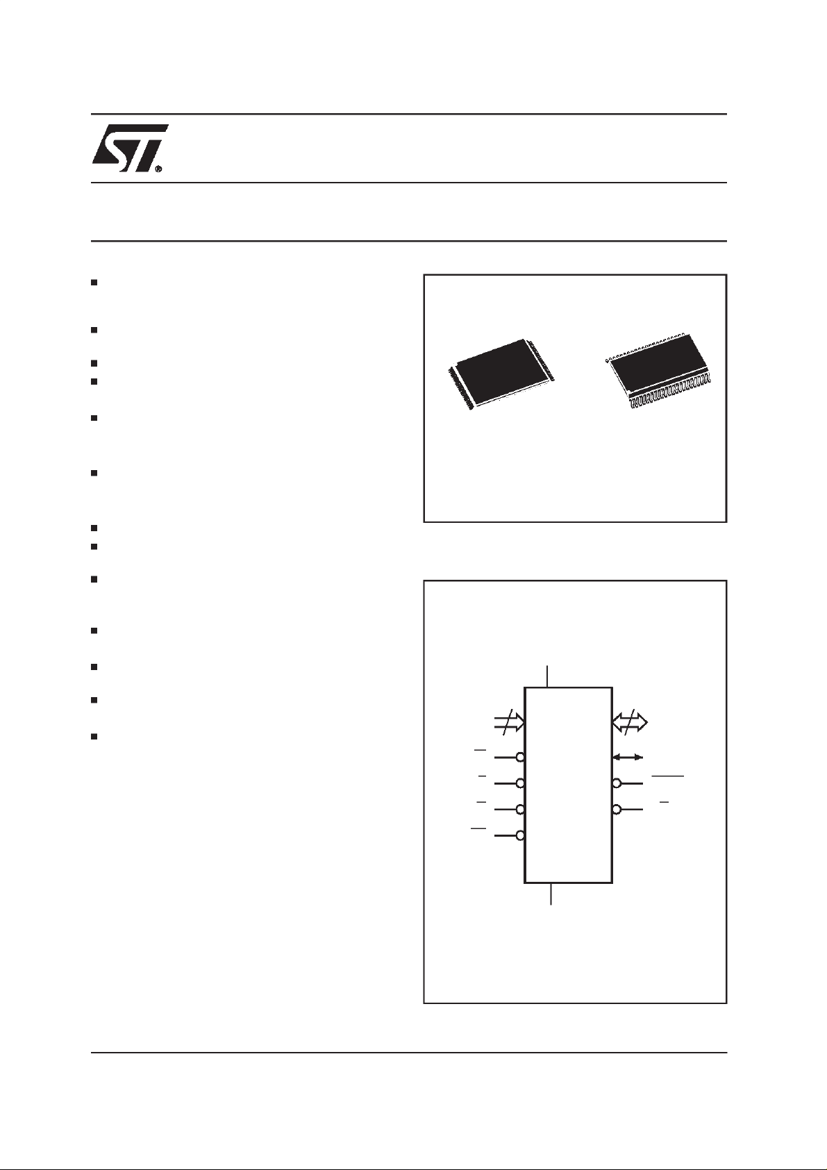
M29F400T
M29F400B
Single Supply Flash Memory
NOT FOR NEW DESIGN
44
1
12 x 20mm
Figure1. Logic Diagram
V
CC
18
A0-A17
W
E
G
RP
M29F400T
M29F400B
V
SS
SO44 (M)TSOP48 (N)
15
DQ0-DQ14
DQ15A–1
BYTE
RB
AI01726B
November 1999 1/34
This is information on a productstil l in production but not recommendedfor new designs.
Page 2
M29F400T, M29F400B
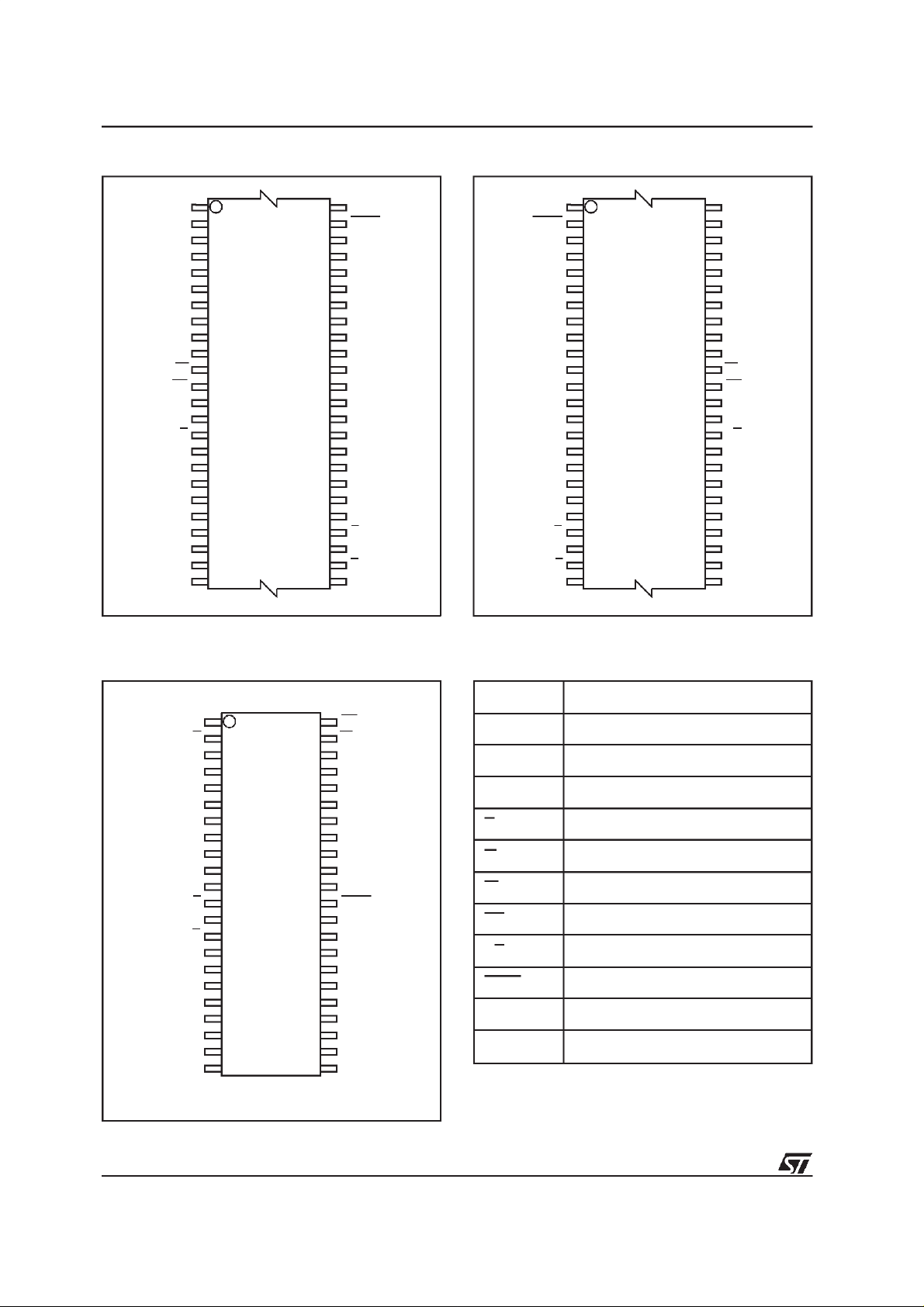
Figure 2A. TSOP Pin Connections
A15
1
A14
A13
A12
A11
A10 DQ14
A9
A8
NC
NC
W
RP
NC
NC
RB
NC
A17
A7
A6
A5
A4
A3
A2
A1
M29F400T
12
M29F400B
13
(Normal)
24 25
48
37
36
AI01727B
A16
BYTE
V
SS
DQ15A–1
DQ7
DQ6
DQ13
DQ5
DQ12
DQ4
V
CC
DQ11
DQ3
DQ10
DQ2
DQ9
DQ1
DQ8
DQ0
G
V
SS
E
A0
Figure 2B. TSOP Reverse Pin Connections
A15
A16
BYTE
V
SS
DQ15A–1
DQ7
DQ14
DQ6
DQ13
DQ5
DQ12
DQ4
V
CC
DQ11
DQ3
DQ10
DQ2
DQ9
DQ1
DQ8
DQ0
V
SS
A0
1
M29F400T
12
M29F400B
13
(Reverse)
G
E
24 25
48
37
36
AI01728B
A14
A13
A12
A11
A10
A9
A8
NC
NC
W
RP
NC
NC
RB
NC
A17
A7
A6
A5
A4
A3
A2
A1
Warning: NC = Not Connected. Warning: NC = Not Connected.
Figure 2C. SO Pin Connections
Table 1. Signal Names
A0-A17 Address Inputs
NC RP
1
2
3
A17 A8
A7
4
5
A6
6
A5
A4
7
A3
8
A2
9
A1
10
A0
11
M29F400T
M29F400B
12
13
14
15
16
17DQ1
18
19
20
21
V
SS
DQ0
DQ8
DQ9
DQ10
DQ3
DQ11
E
G
44
43
42
41
40
39
38
37
36
35
34
33
32
31
30
29
28
27
26
25
24
2322
AI01729B
WRB
A9
A10
A11
A12
A13
A14
A15
A16
BYTE
V
SS
DQ15A–1
DQ7
DQ14
DQ6
DQ13
DQ5DQ2
DQ12
DQ4
V
CC
DQ0-DQ7 Data Input/Outputs, Command Inputs
DQ8-DQ14 Data Input/Outputs
DQ15A–1 Data Input/Output or Address Input
E Chip Enable
G Output Enable
W Write Enable
RP Reset / Block TemporaryUnprotect
RB Ready/Busy Output
BYTE Byte/Word Organisation
V
CC
V
SS
Supply Voltage
Ground
Warning: NC = Not Connected.
2/34
Page 3

M29F400T, M29F400B
Table 2. AbsoluteMaximum Ratings
Symbol Parameter Value Unit
T
A
T
BIAS
T
STG
(2)
V
IO
V
CC
V
(A9, E, G, RP)
Notes: 1. Except for the rating ”Operating Temperature Range”, stresses above those listedin theTable ”Absolute Maximum Ratings”
may cause permanent damage to the device. These are stress ratings only andoperation of thedevice at these or any other
conditions above those indicated in the Operating sections of this specification is not implied. Exposure to Absolute Maximum
Rating conditions for extended periods may affect device reliability.Refer also to the STMicroelectronicsSUREProgram and other
relevant qualitydocuments.
2. Minimum Voltage may undershoot to –2V during transition and for less than 20ns.
3. Depends on range.
Ambient Operating Temperature
TemperatureUnder Bias –50 to 125
Storage Temperature –65 to 150 °C
Input or OutputVoltages –0.6 to 7 V
Supply Voltage –0.6 to 7 V
(2)
A9, E, G, RP Voltage –0.6 to 13.5 V
DESCRIPTION (Cont’d)
graming and erase on programming equipment,
and temporarily unprotected to make changes in
the application.
Instructions for Read/Reset, Auto Select for reading the Electronic Signature or Block Protection
status,Programming, BlockandChipErase,Erase
Suspend and Resume are written to the devicein
cyclesof commandstoa CommandInterfaceusing
standard microprocessor write timings.
The device is offeredin TSOP48 (12x 20mm) and
SO44packages. Both normal and reversepinouts
are available for the TSOP48 package.
Organisation
TheM29F400 is organisedas512Kx8or 256Kx16
bitsselectable by the BYTE signal. When BYTEis
Low the Byte-widex8 organisation is selectedand
the address lines are DQ15A–1 and A0-A17. The
Data Input/Output signal DQ15A–1 acts as address line A–1 which selects the lower or upper
Byte of the memory wordfor output on DQ0-DQ7,
DQ8-DQ14 remain at High impedance. When
BYTEis High the memoryuses theaddress inputs
A0-A17 and the Data Input/Outputs DQ0-DQ15.
Memory control is provided by Chip Enable E,
OutputEnable G and Write Enable W inputs.
AReset/Block TemporaryUnprotection RPtri-level
input provides a hardware reset when pulled Low,
andwhenheld High(atVID)temporarily unprotects
blocks previously protected allowing them to be
programed anderased.Eraseand Program operations are controlled by an internal Program/Erase
Controller (P/E.C.). Status Registerdata output on
DQ7provides a Data Pollingsignal, and DQ6 and
(1)
(3)
–40 to 125
DQ2provide Toggle signals to indicate thestate of
the P/E.C operations. A Ready/Busy RB output
indicates the completionof theinternal algorithms.
MemoryBlocks
The devices feature asymmetrically blocked architectureprovidingsystem memoryintegration.Both
M29F400Tand M29F400B devices have an array
of 11 blocks, one Boot Block of 16 KBytes or 8
KWords, two Parameter Blocks of 8 KBytes or 4
KWords, one Main Block of 32 KBytes or 16
KWords and sevenMainBlocksof 64KBytesor32
KWords. The M29F400T has the Boot Blockat the
top of the me mor y addre ss spac e and t he
M29F400B locates the Boot Block starting at the
bottom. The memory maps are showed in Figure
3. Eachblock can be erasedseparately, any combination of blocks can be specified for multi-block
eraseor the entire chip may be erased. The Erase
operations are managed automatically by the
P/E.C. The block erase operation can be suspended in order to read from or program to any
block not being ersased, and then resumed.
Block protection provides additional data security.
Each block can be separately protected or unprotected against Program or Erase on programming
equipment. All previously protected blocks can be
temporarily unprotected in the application.
Bus Operations
The following operations can be performed using
the appropriate bus cycles:Read(Array, Electronic
Signature, Block Protection Status), Write command,Output Disable, Standby, Reset, Block Protect ion, Unprotection, Protection Verify,
Unprotection Verify and Block Temporary Unpro-
C
°
C
°
tection. See Tables 4 and5.
3/34
Page 4
M29F400T, M29F400B
Figure 3. MemoryMap and Block Address Table (x8)
7FFFFh
7C000h
7BFFFh
7A000h
79FFFh
78000h
77FFFh
70000h
6FFFFh
60000h
5FFFFh
50000h
4FFFFh
40000h
3FFFFh
30000h
2FFFFh
20000h
1FFFFh
10000h
0FFFFh
00000h
M29F400T
16K BOOT BLOCK
8K PARAMETER BLOCK
8K PARAMETER BLOCK
32K MAIN BLOCK
64K MAIN BLOCK
64K MAIN BLOCK
64K MAIN BLOCK
64K MAIN BLOCK
64K MAIN BLOCK
64K MAIN BLOCK
64K MAIN BLOCK
7FFFFh
70000h
6FFFFh
60000h
5FFFFh
50000h
4FFFFh
40000h
3FFFFh
30000h
2FFFFh
20000h
1FFFFh
10000h
0FFFFh
08000h
07FFFh
06000h
05FFFh
04000h
03FFFh
00000h
M29F400B
64K MAIN BLOCK
64K MAIN BLOCK
64K MAIN BLOCK
64K MAIN BLOCK
64K MAIN BLOCK
64K MAIN BLOCK
64K MAIN BLOCK
32K MAIN BLOCK
8K PARAMETER BLOCK
8K PARAMETER BLOCK
16K BOOT BLOCK
AI01730
CommandInterface
Instructions, made up of commands written in cycles,can be given to the Program/Erase Controller
through a Command Interface (C.I.). For added
data protection, program or erase execution starts
after4 or6 cycles.The first,second,fourthand fifth
cycles are used to input Coded cycles to the C.I.
This Coded sequence is the same for all Program/Erase Controller instructions. The ’Command’itself and its confirmation,when applicable,
are given on the third, fourth or sixth cycles. Any
incorrect command or any improper commandsequence will reset the device toRead Array mode.
Instructions
Seven instructions are defined to perform Read
Array, Auto Select(to readthe ElectronicSignature
or BlockProtection Status),Program, BlockErase,
Chip Erase, Erase Suspend and Erase Resume.
The internal P/E.C. automatically handles all timing and verification of the Program and Erase
operations. The StatusRegister Data Polling,Toggle, Error bits and the RB output may be read at
4/34
any time, duringprogramming or erase,to monitor
the progressof the operation.
Instructions are composed of upto six cycles. The
first two cycles input a Coded sequence to the
CommandInterfacewhichis commonto allinstructions (see Table 8). The third cycle inputs the
instruction set-up command. Subsequent cycles
outputthe addressed data, Electronic Signature or
Block Protection Status for Read operations. In
orderto giveadditional dataprotection, theinstructions for Program and Block or ChipErase require
furthercommand inputs.For a Programinstruction,
the fourth command cycle inputs the address and
data to be programmed. For an Erase instruction
(Block or Chip), the fourth and fifth cycles input a
further Coded sequence before the Erase confirm
commandon the sixth cycle. Erasureof a memory
blockmaybe suspended, inordertoreaddatafrom
anotherblock or to programdata in anotherblock,
and then resumed.
When power is first applied or if VCCfalls below
V
, the command interface is reset to Read
LKO
Array.
Page 5
M29F400T, M29F400B
Table 3A. M29F400T Block Address Table
Address Range (x8) Address Range (x16) A17 A16 A15 A14 A13 A12
00000h-0FFFFh 00000h-07FFFh 0 0 0 X X X
10000h-1FFFFh 08000h-0FFFFh 0 0 1 X X X
20000h-2FFFFh 10000h-17FFFh 0 1 0 X X X
30000h-3FFFFh 18000h-1FFFFh 0 1 1 X X X
40000h-4FFFFh 20000h-27FFFh 1 0 0 X X X
50000h-5FFFFh 28000h-2FFFFh 1 0 1 X X X
60000h-6FFFFh 30000h-37FFFh 1 1 0 X X X
70000h-77FFFh 38000h-3BFFFh 1 1 1 0 X X
78000h-79FFFh 3C000h-3CFFFh 1 1 1 1 0 0
7A000h-7BFFFh 3D000h-3DFFFh 1 1 1 1 0 1
7C000h-7FFFFh 3E000h-3FFFFh 1 1 1 1 1 X
Table 3B. M29F400B Block Address Table
Address Range (x8) Address Range (x16) A17 A16 A15 A14 A13 A12
00000h-03FFFh 00000h-01FFFh 0 0 0 0 0 X
04000h-05FFFh 02000h-02FFFh 0 0 0 0 1 0
06000h-07FFFh 03000h-03FFFh 0 0 0 0 1 1
08000h-0FFFFh 04000h-07FFFh 0 0 0 1 X X
10000h-1FFFFh 08000h-0FFFFh 0 0 1 X X X
20000h-2FFFFh 10000h-17FFFh 0 1 0 X X X
30000h-3FFFFh 18000h-1FFFFh 0 1 1 X X X
40000h-4FFFFh 20000h-27FFFh 1 0 0 X X X
50000h-5FFFFh 28000h-2FFFFh 1 0 1 X X X
60000h-6FFFFh 30000h-37FFFh 1 1 0 X X X
70000h-7FFFFh 38000h-3FFFFh 1 1 1 X X X
5/34
Page 6

M29F400T, M29F400B
SIGNALDESCRIPTIONS
See Figure 1 and Table1.
AddressInputs (A0-A17). The addressinputs for
thememoryarrayare latchedduringa writeoperation on the falling edge of Chip Enable E or Write
Enable W. In Word-wide organisation the address
lines are A0-A17, in Byte-wi de organisation
DQ15A–1 acts as an additional LSB address line.
WhenA9 is raised to VID, either a Read Electronic
Signature Manufacturer or Device Code, Block
Protection Status or a Write Block Protection or
Block Unprotection is enabled depending on the
combination of levelson A0, A1,A6, A12 and A15.
Data Input/Outputs (DQ0-DQ7). These Inputs/Outputsare used in theByte-wide and Wordwide or ganisatio ns. The i nput is data to be
programmed in the memory array or a command
to be written to the C.I. Both are latched on the
rising edge of Chip Enable E or Write Enable W.
The output is data from the Memory Array, the
Electronic Signature Manufacturer or Device
codes, the Block Protection Status or the Status
register Data Pollingbit DQ7, the Toggle Bits DQ6
and DQ2, the Error bit DQ5 or the Erase Timer bit
DQ3. Outputs are valid when Chip Enable E and
Output Enable G are active. The output is high
impedance when the chip is deselected or the
outputsaredisabledandwhen RP isata Lowlevel.
Data Input/Outputs (DQ8-DQ14 and DQ15A–1).
These Inputs/Outputs are additionally used in the
Word-wideorganisation.When BYTEisHighDQ8DQ14 and DQ15A–1 act as the MSB of the Data
Input or Output, functioning as describedforDQ0DQ7 above, and DQ8-DQ15 are ’don’t care’ for
command inputs or status outputs. When BYTEis
Low,DQ8-DQ14are highimpedance, DQ15A–1is
the Address A–1input.
Chip Enable (E). The Chip Enable input activates
the memory control logic, input buffers, decoders
andsenseamplifiers.EHighdeselectsthememory
andreducesthe powerconsumptionto thestandby
level. E can also be used to control writing to the
command register and to the memoryarray, while
Wremainsat a lowlevel.The ChipEnablemustbe
forcedto VIDduringtheBlockUnprotection operation.
Output Enable (G). The Output Enable gates the
outputs through the data buffers during a read
operation. When G is High the outputs are High
impedance. G must be forced to VIDlevel during
BlockProtection and Unprotectionoperations.
WriteEnable(W). This input controlswriting tothe
CommandRegisterandAddressand Datalatches.
Byte/Word Organization Select (BYTE). The
BYTEinput selectstheoutputconfiguration forthe
device: Byte-wide (x8) mode or Word-wide (x16)
mode. When BYTEis Low, the Byte-wide mode is
selectedand the data is read andprogrammed on
DQ0-DQ7. In this mode, DQ8-DQ14 are at high
impedance and DQ15A–1 is the LSB address.
When BYTE is High, the Word-wide mode is selected and the data is read and programmed on
DQ0-DQ15.
Ready/Busy Output (RB). Ready/Busy is an
open-drainoutputandgivestheinternalstateof the
P/E.C.of the device. When RB is Low,the device
is Busy with a Program or Erase operation and it
will not accept any additional program or erase
instructionsexcept the Erase Suspendinstruction.
WhenRB isHigh, thedeviceis readyfor anyRead,
Program or Erase operation. The RB will also be
High when the memory is put in EraseSuspend or
Standbymodes.
Reset/Block Temporary Unprotect Input (RP).
The RP Input provides hardware reset and protected block(s) temporary unprotection functions.
Reset of the memory is acheived by pulling RP to
VILfor at least 500ns. When the reset pulse is
given,if the memoryis in Reador Standby modes,
it will be available for new operations in 50ns after
the rising edge of RP. If the memory is in Erase,
Erase Suspend or Program modes the reset will
take 10µs during which the RB signal will be held
atVIL.Theendofthe memoryresetwillbeindicated
by the rising edge of RB.A hardware reset during
anEraseor Program operationwill corruptthe data
being programmed or the sector(s)being erased.
Temporary block unprotection is made by holding
RP at VID. In this condition previously protected
blocks can be programmed or erased. The transition of RP from VIHto VIDmust slower than 500ns.
When RP is returned from VIDto VIHall blocks
temporarily unprotected will be again protected.
VCCSupply Voltage. The power supply for all
operations (Read, Program and Erase).
VSSGround. VSSis the reference for all voltage
measurements.
6/34
Page 7

M29F400T, M29F400B
DEVICE OPERATIONS
See Tables 4, 5 and 6.
Read. Read operations are used to output the
contents of the Memory Array, the Electronic Signature,the Status Register or the BlockProtection
Status. Both Chip Enable E andOutputEnable G
must be low in order to read the output of the
memory.
Write.Writeoperationsare used to giveInstruction
Commands to the memory or to latch input datato
be programmed. Awrite operationis initiatedwhen
Chip Enable E is Low and Write Enable W is Low
withOutput Enable G High.Addresses arelatched
onthe fallingedge of W or E whicheveroccurs last.
CommandsandInputDataarelatchedontherising
edge of W or E whicheveroccurs first.
OutputDisable. Thedataoutputs are highimpedancewhen the Output Enable G isHigh withWrite
EnableW High.
Standby. The memory is in standby when Chip
Enable E isHigh and the P/E.C.is idle. The power
consumption is reduced to the standby level and
the outputs are high impedance, independent of
the OutputEnable G or WriteEnable W inputs.
Automatic Standby. After 150ns of bus inactivity
andwhen CMOSlevels are drivingthe addresses,
the chip automatically enters a pseudo-standby
modewhereconsumptionis reducedto theCMOS
standbyvalue, while outputs still drive the bus.
Electronic Signature. Two codes identifying the
manufacturer andthe device canbe read fromthe
memory. The manufacturer’s code for STMicroelectronics is20h,the devicecodeisD5hforthe
M29F400T (TopBoot) and D6h for the M29F400B
(Bottom Boot). These codes allow programming
equipment or applications to automatically match
their inter f ace t o t he c har acteri s t ic s of t he
M29F400. The Electronic Signature is output by a
Read operation when the voltage applied to A9 is
atVIDandaddressinputsA1 isLow.The manufacturer code is output when the Address input A0 is
Low and the device code when this input is High.
Other Address inputs are ignored. The codes are
output on DQ0-DQ7.
The ElectronicSignature can alsobe read,without
raisingA9 to VID, by giving the memory the Instruction AS. If the Byte-wide configuration is selected
thecodes areoutputonDQ0-DQ7with DQ8-DQ14
at High impedance; if the Word-wide configuration
is selected the codes are outputonDQ0-DQ7with
DQ8-DQ15at 00h.
Block Protection. Each block can be separately
protected against Program or Erase on programming equipment. Block protection provides additional data security, as it disables all program or
eraseoperations. Thismodeisactivatedwhenboth
A9 and G are raised to VIDand an address in the
blockis applied on A12-A17. The Block Protection
algorithm is shownin Figure 14. Blockprotectionis
initiated on the edge of W fallingto VIL. Then after
a delay of 100µs, the edge of W rising to VIHends
the protectionoperations. Blockprotectionverify is
achieved by bringingG, E, A0 and A6to VILandA1
to VIH, whileW isat VIHandA9 at VID. Underthese
conditions, reading the data output will yield 01h if
the block defined by the inputs on A12-A17 is
protected. Any attempt to program or erase a protected block will be ignored by the device.
Block Temporary Unprotection. Any previously
protected block can be temporarily unprotected in
orderto change storeddata.The temporaryunprotection mode is activated by bringing RP to VID.
During the temporary unprotection mode the previously protected blocks are unprotected. A block
can be selected and data can be modified by
executingtheEraseor Programinstructionwiththe
RPsignalheld at VID. When RP isreturned to VIH,
all the previously protected blocks are again protected.
Block Unprotection. All protected blocks can be
unprotected on programming equipment to allow
updating of bit contents. All blocks must first be
protected before the unprotection operation. Block
unprotection is activatedwhen A9, G and E are at
VIDand A12, A15 at VIH. The Block Unprotection
algorithm is shown in Figure 15. Unprotection is
initiatedbytheedge of Wfallingto VIL.Aftera delay
of 10ms, the unprotection operation will end. Unprotection verify is achievedbybringing G and E to
VILwhileA0 is at VIL, A6 and A1 are at VIHand A9
remains at VID. In these conditions, reading the
outputdata willyield 00h if the blockdefined by the
inputsA12-A17 has beensuccesfullyunprotected.
Eachblockmustbe separatelyverifiedbygiving its
addressin order to ensure that it has been unprotected.
7/34
Page 8
M29F400T, M29F400B
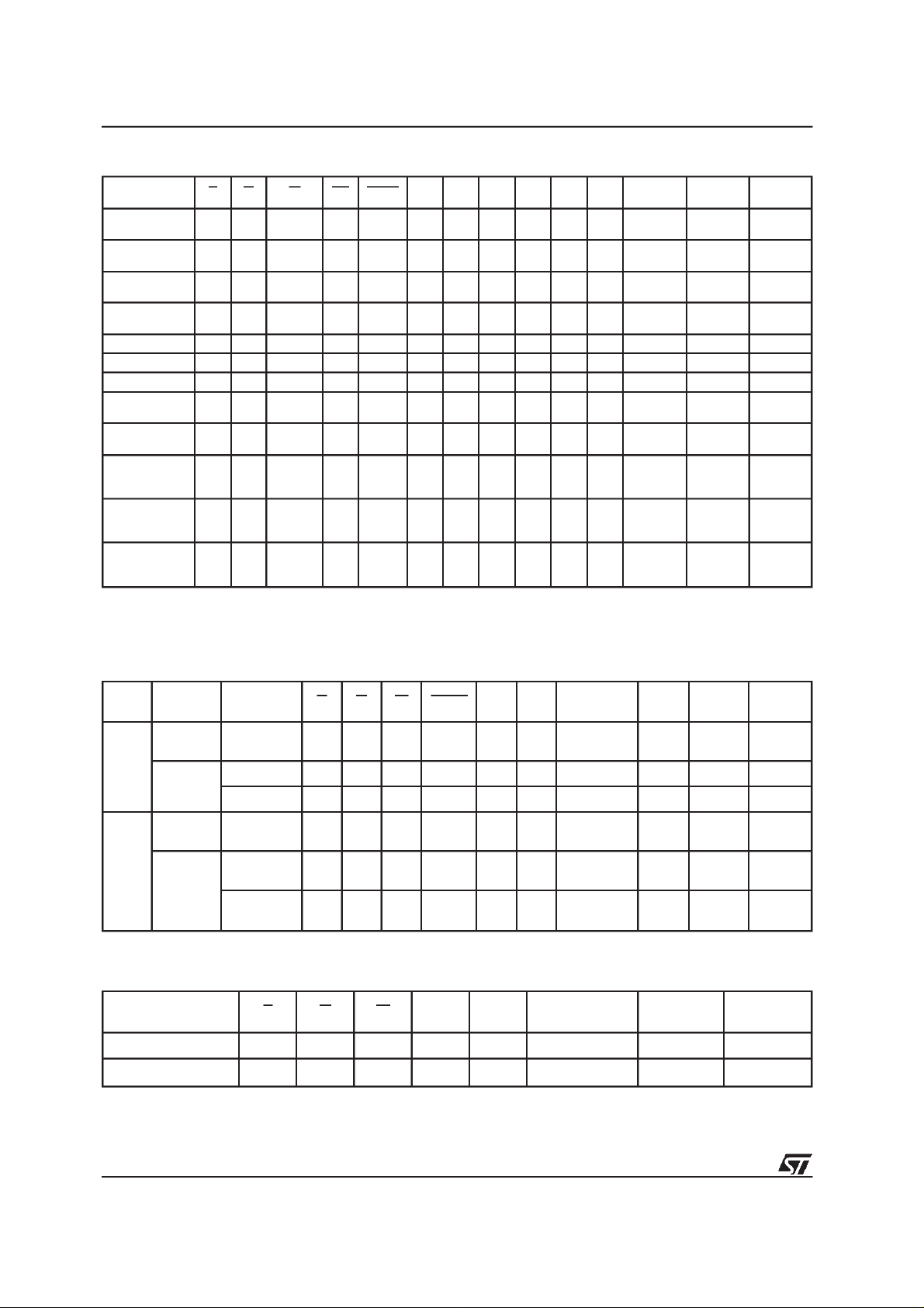
Table 4. User Bus Operations
(1)
Operation E G W RP BYTE A0 A1 A6 A9 A12 A15
Read Word V
Read Byte V
Write Word V
Write Byte V
Output Disable V
Standby V
ILVIL
ILVIL
ILVIH
ILVIH
ILVIH
IH
Reset X X X V
Block
Protection
Blocks
Unprotection
Block
Protection
(2,4)
Verify
Block
Unprotection
(2,4)
Verify
Block
Temporary
Unprotection
Notes: 1. X = V
2. Block Address must be givenon A12-A17bits.
3. See Table6.
VILVIDVILPulse V
(2,4)
VIDVIDVILPulse V
(4)
VILV
VILV
XX X V
or V
IL
IH
V
V
V
IH
IH
V
V
IH
IH
V
V
IL
IH
V
V
IL
IH
V
V
IH
IH
A0 A1 A6 A9 A12 A15
IH
V
A0 A1 A6 A9 A12 A15
IL
V
A0 A1 A6 A9 A12 A15 Data Input Data Input
IH
V
A0 A1 A6 A9 A12 A15
IL
X XXXXXX Hi-Z Hi-Z Hi-Z
XXVIHX XXXXXX Hi-Z Hi-Z Hi-Z
X XXXXXX Hi-Z Hi-Z Hi-Z
IL
XXXXVIDXX X X X
IH
XXXXVIDVIHV
IH
V
V
IL
IH
V
IL
IH
XVILVIHVILVIDA12 A15 X X
IH
V
XVILVIHVIHVIDA12 A15 X X
IH
X XXXXXX X X X
ID
4. Operation performed on programming equipment.
IH
DQ15
A–1
Data
Output
Address
Input
Address
Input
DQ8-
DQ14
Data
Output
Hi-Z
Hi-Z
DQ0-DQ7
Data
Output
Data
Output
Data
Input
Data
Input
XXX
Block
Protect
Status
Block
Protect
Status
(3)
(3)
Table5. ReadElectronic Signature (following AS instruction or with A9 = VID)
Org. Code Device E G W BYTE A0 A1
Word-
wide
Manufact.
Code
Device
Code
Manufact.
Code
M29F400T V
M29F400B V
VILV
V
IL
VILV
IL
VILV
IL
VILV
V
IL
V
IH
V
IH
V
IH
V
IH
VILVILDon’t Care 0 00h 20h
IH
V
IH
IH
IH
V
IH
VILVILDon’t Care
IL
Byte-
wide
Device
M29F400T V
IL
VILV
V
IH
V
IL
IH
Code
M29F400B V
IL
VILV
V
IH
V
IL
IH
Other
Addresses
VILDon’t Care 0 00h D5h
VILDon’t Care 0 00h D6h
VILDon’t Care
VILDon’t Care
DQ15
A–1
Don’t
Care
Don’t
Care
Don’t
Care
Table6. Read Block Protection with AS Instruction
Code E G W A0 A1 A12 - A17
Protected Block V
Unprotected Block V
IL
IL
V
IL
V
IL
V
IH
V
IH
V
IL
V
IL
V
IH
V
IH
BlockAddress Don’t Care 01h
BlockAddress Don’t Care 00h
Addresses
Other
DQ8 DQ14
DQ0 -
DQ7
Hi-Z 20h
Hi-Z D5h
Hi-Z D6h
DQ0 - DQ7
8/34
Page 9
M29F400T, M29F400B
INSTRUCTIONSAND COMMANDS
The Command Interface latches commands written to the memory. Instructions are made up from
one or more commandsto perform Read Memory
Array, Read Electronic Signature, ReadBlockProtection, Program, Block Erase, Chip Erase, Erase
Suspend and Erase Resume. Commands are
made of address and data sequences. The instructionsrequirefrom 1 to6 cycles,the firstor first
three of which are alwayswrite operations used to
initiatetheinstruction.They are followed by either
furtherwrite cycles to confirmthe first commandor
executethe commandimmediately. Commandsequencing must be followed exactly. Any invalid
combination of commands will reset the device to
Read Array. The increased number of cycles has
been chosen to assure maximum data security.
Instructions are initialised by twoinitial Coded cycleswhich unlock theCommand Interface.In addition, for Erase, instruction confirmation is again
preceded by the two Coded cycles.
StatusRegister Bits
P/E.C.statusis indicatedduringexecutionby Data
Polling on DQ7, detection of Toggle on DQ6 and
DQ2, or Error on DQ5 and Erase Timer DQ3 bits.
Any read attempt during Program or Erase commandexecutionwillautomatically output thesefive
StatusRegisterbits.The P/E.C.automatically sets
bits DQ2, DQ3, DQ5, DQ6 and DQ7. Other bits
(DQ0, DQ1 and DQ4) are reserved for future use
and should be masked. See Tables 9 and 10.
Data Polling Bit (DQ7). When Programming operations are in progress, this bit outputs the complement of the bit being programmed on DQ7.
DuringErase operation, it outputs a ’0’.After completionof the operation, DQ7 will outputthebit last
programmed or a ’1’ after erasing. Data Polling is
valid and only effective during P/E.C. operation,
that is after the fourth W pulse for programming or
after the sixth W pulse for erase. It must be performed at theaddress being programmed or at an
address within the block being erased. If all the
blocksselectedfor erasureare protected, DQ7will
be setto ’0’for about100µs, and thenreturn to the
previous addressed memory data value. See Figure 11for the Data Pollingflowchart and Figure 10
for the Data Polling waveforms. DQ7 will also flag
the Erase Suspend mode by switching from ’0’ to
’1’ at the start of the Erase Suspend. In order to
monitor DQ7 in the Erase Suspend mode an address within a block being erased must be provided. For a Read Operation in Erase Suspend
mode, DQ7 will output ’1’ if the read is attempted
onablockbeing erasedandthedatavalueon other
blocks. During Program operation in Erase SuspendMode, DQ7 will have the same behaviour as
in the normal program execution outside of the
suspend mode.
ToggleBit (DQ6). When Programming or Erasing
operations are in progress,successiveattemptsto
readDQ6will outputcomplementarydata.DQ6 will
toggle following toggling of either G, or E when G
is low. The operation is completed when two successivereadsyieldthe sameoutput data.The next
readwilloutputthe bitlastprogrammed ora’1’after
erasing. The toggle bit DQ6 is valid only during
P/E.C.operations, that is after the fourth W pulse
for programming or after the sixth W pulse for
Erase. If the blocks selected for erasure are protected, DQ6 will toggle for about 100µs and then
returnbackto Read. DQ6willbe setto’1’if a Read
operation is attemptedonan EraseSuspend block.
When erase is suspended DQ6 will toggle during
programming operations in a blockdifferent to the
block in Erase Suspend. Either E or G toggling will
cause DQ6 to toggle.See Figure 12 for Toggle Bit
flowchartand Figure 13 for Toggle Bit waveforms.
Table 7. Commands
Hex Code Command
00h Invalid/Reserved
10h Chip Erase Confirm
20h Reserved
30h Block Erase Resume/Confirm
80h Set-up Erase
90h
A0h Program
B0h Erase Suspend
F0h Read Array/Reset
Read Electronic Signature/
Block Protection Status
9/34
Page 10
M29F400T, M29F400B
Table 8. Instructions
(1)
Mne. Instr. Cyc. 1st Cyc. 2ndCyc. 3rdCyc. 4th Cyc. 5th Cyc. 6th Cyc. 7th Cyc.
(3,7)
RD
Read/Reset
(2,4)
Memory Array
Addr.
1+
Data F0h
Byte
(3,7)
Addr.
3+
Word 5555h 2AAAh 5555h
X
Read Memory Array until a new write cycle is initiated.
AAAAh 5555h AAAAh
Read Memory Array until a new write cycle
is initiated.
Data AAh 55h F0h
(4)
Auto Select 3+
AS
Addr.
(3,7)
Word 5555h 2AAAh 5555h
Read Electronic Signature or Block
Protection Status until a new write cycle is
initiated. See Note 5 and 6.
Byte AAAAh 5555h AAAAh
Data AAh 55h 90h
PG Program 4
BE Block Erase 6
Byte AAAAh 5555h AAAAh
(3,7)
Addr.
Word 5555h 2AAAh 5555h
Data AAh 55h A0h
Byte AAAAh 5555h AAAAh AAAAh 5555h
(3,7)
Addr.
Word 5555h 2AAAh 5555h 5555h 2AAAh
Program
Address
Program
Data
Read Data Polling or Toggle Bit
until Program completes.
Block
Address
Additional
Data AAh 55h 80h AAh 55h 30h 30h
CE Chip Erase 6
Addr.
Word 5555h 2AAAh 5555h 5555h 2AAAh 5555h
Byte AAAAh 5555h AAAAh AAAAh 5555h AAAAh
(3,7)
Data AAh 55h 80h AAh 55h 10h
(3,7)
(10) Erase
ES
Notes: 1. Commands not interpreted in this table will defaulttoread array mode.
Suspend
Erase
ER
Resume
2. Await of t
before startingany new operation (seeTable14 and Figure9).
3. X = Don’t Care.
4. The first cycles of the RD or AS instructions are followed by read operations. Any number of readcycles canoccur after
the command cycles.
5. SignatureAddress bits A0,A1 at V
Device code.
6. Block Protection Address: A0 atV
7. For Coded cycles address inputs A15-A17 are don’t care.
8. Optional, additional Blocks addresses must be entered within the erase timeout delayafter last write entry,
timeout status can be verified through DQ3 value (see Erase TimerBit DQ3 description).
When full command is entered, read DataPolling or Togglebit until Erase is completed or suspended.
9. Read Data Polling, Togglebits or RB until Erase completes.
10.During Erase Suspend,Readand DataProgram functions are allowedin blocks not being erased.
is necessary after a Read/Resetcommand if the memory was in an Erase or Program mode
PLYH
Addr.
1
Data B0h
(3,7)
Addr.
1
Data 30h
will output Manufacturer code (20h).Address bits A0 at VIHandA1 at VILwill output
IL
,A1atVIHand A12-A17 within the Blockwill output the Block Protection status.
IL
X
Read until Toggle stops, then read all the data needed from any
Block(s) not being erased then ResumeErase.
X
Read Data Polling or ToggleBits until Erase completes or Erase is
suspended another time
Block
Note 9
(8)
10/34
Page 11
M29F400T, M29F400B
Table9. Status RegisterBits
DQ Name Logic Level Definition Note
Erase Complete or erase
block in Erase Suspend
Program Complete or data
of non erase block during
Erase Suspend
Erase Complete or Erase
Suspend on currently
addressed block
Indicates the P/E.C. status, check during
Program or Erase, and on completion
before checking bits DQ5 for Program or
Erase Success.
data on DQ6 while Programming or Erase
operations are on-going. DQ6 remains at
constant level when P/E.C. operations are
completed or Erase Suspend is
acknowledged.
Data
7
Polling
6 ToggleBit
’1’
’0’ Erase On-going
DQ
DQ Program On-going
’-1-0-1-0-1-0-1-’ Erase or Program On-going Successive reads output complementary
DQ Program Complete
’-1-1-1-1-1-1-1-’
5 Error Bit
4 Reserved
Erase
3
TimeBit
2 ToggleBit
1 Reserved
0 Reserved
Note:
Logic level ’1’ is High, ’0’ is Low. -0-1-0-0-0-1-1-1-0- represent bit value in successive Read operations.
’1’ Program or Erase Error
’0’ Program or Erase On-going
’1’ Erase Timeout Period Expired
’0’
’-1-0-1-0-1-0-1-’
1
DQ
Erase Timeout Period
On-going
Chip Erase, Erase or Erase
Suspend on the currently
addressed block.
Erase Error due to the
currently addressed block
(when DQ5 = ’1’).
Program on-going, Erase
on-going on another block or
Erase Complete
Erase Suspend read on
non Erase Suspend block
This bit is set to ’1’ in the case of
Programming or Erase failure.
P/E.C. Erase operation has started. Only
possible command entry is Erase Suspend
(ES).
An additional block to be erased in parallel
can be entered to the P/E.C.
Indicates the erase status and allows to
identify the erased block
11/34
Page 12

M29F400T, M29F400B
Table 10. Polling and Toggle Bits
Mode DQ7 DQ6 DQ2
Program DQ7 Toggle 1
Erase 0 Toggle Note 1
Erase Suspend Read
(in Erase Suspend
block)
Erase Suspend Read
(outside Erase Suspend
block)
Erase Suspend Program DQ7 Toggle N/A
Note: 1. Toggle if the address is within a block being erased.
’1’ if the address is within a block not being erased.
1 1 Toggle
DQ7 DQ6 DQ2
Toggle Bit (DQ2). This toggle bit, together with
DQ6, can be used to determine the device status
duringthe Erase operations. It can alsobe used to
identify the block being erased. During Erase or
Erase Suspend a readfrom a block being erased
will cause DQ2 to toggle. A read from a block not
being erased will set DQ2 to ’1’during erase and
to DQ2during Erase Suspend. During Chip Erase
a read operation will cause DQ2 to toggle as all
blocks are being erased. DQ2 will be set to ’1’
duringprogram operation and whenerase iscomplete. After erase completion and if the error bit
DQ5 is set to ’1’,DQ2 will toggle if the faultyblock
is addressed.
ErrorBit (DQ5). Thisbit is set to ’1’ by the P/E.C.
when there is a failure of programming, block
erase, or chip erase that results in invalid data in
thememoryblock.Incase ofanerrorin blockerase
or program, the blockin whichthe error occuredor
to which the programmed data belongs, must be
discarded. The DQ5 failure condition will also appearif a usertriesto programa’1’to alocationthat
is previously programmed to’0’. Other Blocksmay
stillbeused.TheerrorbitresetsafteraRead/Reset
(RD) instruction. In case of success of Program or
Erase,the error bit will be set to ’0’.
Erase Timer Bit (DQ3). This bit is set to ’0’ by the
P/E.C. when the last block Erase command has
been entered to the Command Interface and it is
awaiting the Erase start. When the erase timeout
periodisfinished, after 80µsto120µs, DQ3returns
to ’1’.
CodedCycles
The twoCoded cycles unlock the Command Interface.They are followed by an input commandor a
confirmation command. The Coded cyclesconsist
of writing the data AAh at address AAAAh in the
Byte-wide configuration and at address 5555h in
the Word-wide configuration during the first cycle.
During the secondcycle the Coded cyclesconsist
of writing the data 55h at address 5555h in the
Byte-wide configuration and at address 2AAAh in
the Word-wideconfiguration. In theByte-wideconfigurationthe address linesA–1 to A14arevalid,in
Word-wide A0 toA14are valid,otheraddresslines
are ’don’t care’.The Coded cycles happen on first
and second cyclesof the command write oron the
fourth and fifth cycles.
Instructions
See Table8.
Read/Reset (RD) Instruction. The Read/Reset
instruction consists of one write cycle giving the
commandF0h.Itcanbeoptionallyprecededby the
twoCodedcycles.Subsequent readoperationswill
read the memory array addressed and output the
data read. A wait state of 10µs is necessaryafter
Read/Reset prior to any valid read if the memory
was in an Erase mode when the RD instruction is
given.
Auto Select (AS) Instruction. This instruction
uses the two Coded cycles followed by one write
cycle giving the command 90h to address AAAAh
in the Byte-wide configuration or address 5555h in
the Word-wide configuration for command set-up.
A subsequent read will output the manufacturer
code and the device code or the block protection
status depending on the levels of A0 and A1. The
manufacturer code, 20h, is output when the addresseslines A0 and A1 are Low,the device code,
D5h for Top Boot, D6h for Bottom Boot is output
whenA0 is High with A1 Low.
The AS instruction also allows access to the block
protectionstatus.AftergivingtheASinstruction,A0
is set to VILwith A1 at VIH, while A12-A17 define
the address of the block to be verified. A read in
these conditions will output a 01h if the block is
protectedand a 00h if the block is not protected.
Program (PG) Instruction. This instruction uses
four write cycles. Both for Byte-wide configuration
and for Word-wide configuration. The Program
command A0h is writtento address AAAAh in the
Byte-wide configuration or to address5555h in the
Word-wide configuration on the thirdcycleaftertwo
Codedcycles. Afourth write operation latches the
Addresson the fallingedgeof W or Eand the Data
to be written on the rising edge and starts the
P/E.C.Read operations outputthe StatusRegister
bits after the programming has started. Memory
programming is made only by writing’0’ in placeof
’1’.StatusbitsDQ6and DQ7determineif programmingis on-goingand DQ5allows verificationofany
possible error. Programming at an address not in
blocks being erased is also possible during erase
suspend. In this case, DQ2 will toggle at the address being programmed.
12/34
Page 13

M29F400T, M29F400B
Table 11. ACMeasurement Conditions
High Speed Standard
Input Rise and Fall Times ≤ 10ns ≤ 10ns
Input Pulse Voltages 0 to 3V 0.45V to 2.4V
Input and Output Timing Ref. Voltages 1.5V 0.8V and 2V
Figure 4. AC Testing InputOutput Waveform
High Speed
3V
1.5V
0V
Standard
2.4V
0.45V
Table 12. Capacitance
Symbol Parameter TestCondition Min Max Unit
C
IN
C
OUT
Note: 1. Sampled only,not 100% tested.
Input Capacitance VIN=0V 6 pF
Output Capacitance V
(1)
(TA=25°C,f = 1 MHz )
2.0V
0.8V
AI01275B
Figure5. AC Testing Load Circuit
1.3V
1N914
3.3kΩ
DEVICE
UNDER
TEST
C
L
CL= 30pF for High Speed
CL= 100pF for Standard
CLincludes JIG capacitance
=0V 12 pF
OUT
OUT
AI01276B
Block Erase (BE) Instruction. This instruction
uses a minimum of six write cycles. The Erase
Set-upcommand80h is written to address AAAAh
in the Byte-wide configuration or address5555h in
theWord-wideconfigurationon thirdcycleafterthe
two Codedcycles. The Block Erase Confirm command30his similarlywrittenon thesixthcycleafter
anothertwoCoded cycles. During the input of the
secondcommandan address withintheblocktobe
erasedis givenandlatchedinto the memory.Additional block Erase Confirm commands and block
addresses can be written subsequently to erase
other blocks in parallel, without further Coded cycles. The erase will start after the erase timeout
period (see Erase Timer Bit DQ3 description).
Thus, additional Erase Confirm commands for
other blocks must be given within this delay. The
inputof a newErase Confirm command will restart
the timeoutperiod. The status of the internal timer
can be monitoredthrough the level of DQ3, if DQ3
is ’0’ the Block Erase Command has been given
andthe timeoutis running, ifDQ3is’1’, thetimeout
has expired and the P/E.C.is erasingthe Block(s).
If the second command given is not an erase
confirm or if the Coded cycles are wrong, the
instructionaborts, and the device is reset to Read
Array. It isnot necessaryto programthe block with
00h as the P/E.C. will do this automatically before
to erasing to FFh. Read operations after the sixth
rising edge of W or E output the status register
status bits.
13/34
Page 14

M29F400T, M29F400B
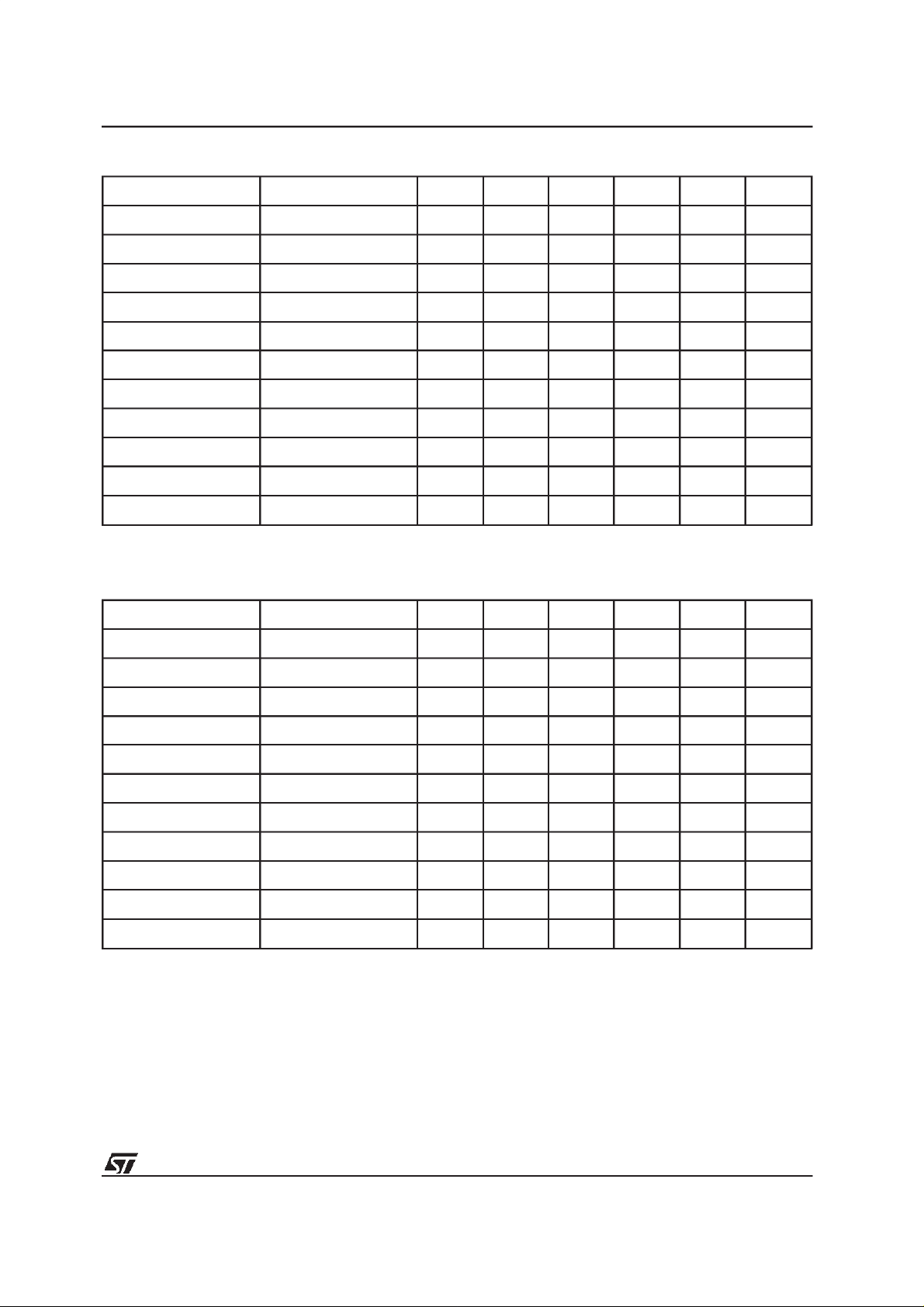
Table 13. DC Characteristics
(TA=0to70°C, –40 to 85°C or –40 to 125°C; VCC=5V±10%)
Symbol Parameter Test Condition Min Max Unit
I
I
LO
I
CC1
I
CC1
I
CC2
I
CC3
I
CC4
V
V
V
V
Input Leakage Current 0V≤V
LI
Output Leakage Current 0V≤V
Supply Current (Read) TTLByte E = VIL,G=VIH, f = 6MHz 20 mA
Supply Current (Read) TTLWord E = VIL,G=VIH, f = 6MHz 20 mA
Supply Current (Standby) TTL E = V
Supply Current (Standby) CMOS E = V
(1)
Supply Current (Program or Erase)
Input Low Voltage –0.5 0.8 V
IL
Input High Voltage 2 VCC+ 0.5 V
IH
Output Low Voltage IOL= 5.8mA 0.45 V
OL
Output High Voltage TTL IOH= –2.5mA 2.4 V
OH
Output High VoltageCMOS I
V
I
V
LKO
Note: 1. Sampled only,not 100% tested.
A9 Voltage(Electronic Signature) 11.0 12.0 V
ID
A9 Current (Electronic Signature) A9 = V
ID
Supply Voltage(Erase and
Program lock-out)
V
≤
IN
CC
V
≤
OUT
CC
IH
0.2V 100
±
CC
Byte program, Block or
Chip Erase in progress
= –100µAV
OH
ID
1
±
1
±
1mA
20 mA
–0.4V V
CC
100
3.2 4.2 V
A
µ
A
µ
A
µ
A
µ
Duringtheexecutionof theeraseby theP/E.C.,the
memoryaccepts only the Erase Suspend ES and
Read/Reset RD instructions. Data Polling bit DQ7
returns’0’ while the erasure is in progress and ’1’
when it has completed. The Toggle bit DQ2 and
DQ6 toggle during the eraseoperation. They stop
when erase is completed. After completion the
StatusRegisterbitDQ5returns’1’iftherehasbeen
an erase failure.In sucha situation, the Toggle bit
DQ2 can be used to determine which block is not
correctly erased. In the case of erase failure, a
Read/Reset RD instructionisnecessary in orderto
reset the P/E.C.
ChipErase(CE)Instruction. Thisinstructionuses
six write cycles. The Erase Set-up command 80h
is written to address AAAAh in the Byte-wideconfiguration or the address 5555h in the Word-wide
14/34
configuration on thethirdcycleafter the twoCoded
cycles. The Chip Erase Confirm command 10h is
similarlywrittenonthe sixth cycleafter anothertwo
Codedcycles.If thesecond command givenis not
an erase confirmor if the Codedcycles are wrong,
the instruction aborts and the device is reset to
ReadArray. It isnotnecessarytoprogramthearray
with00h firstastheP/E.C.willautomaticallydothis
beforeerasing it to FFh. Read operations after the
sixth rising edge of W or E output the Status
Registerbits. During the executionof theerase by
the P/E.C.,Data Pollingbit DQ7returns’0’,then ’1’
on completion. The Toggle bits DQ2 and DQ6
toggleduringerase operation andstopwhenerase
is completed. Aftercompletion the Status Register
bit DQ5 returns ’1’ if there has been an Erase
Failure.
Page 15

Table 14A. Read AC Characteristics
(TA=0to70°C, –40 to 85°C or –40 to 125°C)
Symbol Alt Parameter
t
t
AVAV
t
AVQV
(1)
t
ELQX
(2)
t
ELQV
(1)
t
GLQX
(2)
t
GLQV
t
EHQX
(1)
t
EHQZ
t
GHQX
(1)
t
GHQZ
t
AXQX
(1,3)
t
PLYH
t
PHEL
t
PLPX
t
ELBL
t
ELBH
t
BLQZ
t
BHQV
Notes: 1. Sampled only,not 100% tested.
t
2. G may be delayed by up to t
3. To be considered only if the Reset pulse is given while the memory is in Erase or Programmode.
Address Validto Next Address Valid
RC
t
Address Validto Output Valid
ACC
t
Chip Enable Low to Output Transition G = V
LZ
t
Chip Enable Low to Output Valid G = V
CE
t
Output Enable Low to Output Transition E = V
OLZ
t
Output Enable Low to Output Valid E = V
OE
t
Chip Enable High to Output Transition G = V
OH
t
Chip Enable High to Output Hi-Z G = V
HZ
t
Output Enable High to Output Transition E = V
OH
t
Output Enable High to Output Hi-Z E = V
DF
t
Address Transition to Output Transition
OH
t
RRB
RP Low to Read Mode 10 10 µs
READY
t
RP High to Chip Enable Low 50 50 ns
RH
t
RP Pulse Width 500 500 ns
RP
t
Chip Enable to BYTESwitching Low or
ELFL
t
High
ELFH
BYTESwitching Low to Output
t
FLQZ
High Z
BYTESwitching High to Output
t
FHQV
Valid
ELQV-tGLQV
afterthe falling edge of E without increasing t
Test
Condition
,
E=V
IL
G=V
IL
,
E=V
IL
G=V
IL
IL
IL
IL
IL
IL
IL
IL
IL
,
E=V
IL
G=V
IL
M29F400T, M29F400B
M29F400T / M29F400B
-55 -70
High Speed
Interface
Standard
Interface
Min Max Min Max
55 70 ns
55 70 ns
00ns
55 70 ns
00ns
30 30 ns
00ns
15 20 ns
00ns
15 20 ns
00ns
55ns
15 20 ns
30 30 ns
.
ELQV
Unit
15/34
Page 16

M29F400T, M29F400B
Table 14B. Read AC Characteristics
(TA=0to70°C, –40 to 85°C or –40 to 125°C)
Symbol Alt Parameter
t
t
AVAV
t
AVQV
(1)
t
ELQX
(2)
t
ELQV
(1)
t
GLQX
(2)
t
GLQV
t
EHQX
(1)
t
EHQZ
t
GHQX
(1)
t
GHQZ
t
AXQX
(1,3)
t
PLYH
t
PHEL
t
PLPX
t
ELBL
t
ELBH
t
BLQZ
t
BHQV
Notes: 1. Sampled only,not 100% tested.
t
2. G may be delayed by up to t
3. To be considered only if the Reset pulse is given while the memory is in Erase or Programmode.
Address Validto Next Address Valid
RC
t
Address Validto Output Valid
ACC
t
Chip Enable Low to Output Transition G = V
LZ
t
Chip Enable Low to Output Valid G = V
CE
t
Output Enable Low to Output Transition E = V
OLZ
t
Output Enable Low to Output Valid E = V
OE
t
Chip Enable High to Output Transition G = V
OH
t
Chip Enable High to Output Hi-Z G = V
HZ
t
Output Enable High to Output Transition E = V
OH
t
Output Enable High to Output Hi-Z E = V
DF
t
Address Transition to Output Transition
OH
t
RRB
RP Low to Read Mode 10 10 µs
READY
t
RP High to Chip Enable Low 50 50 ns
RH
t
RP Pulse Width 500 500 ns
RP
t
Chip Enable to BYTESwitching Low or
ELFL
t
High
ELFH
BYTESwitching Low to Output
t
FLQZ
High Z
BYTESwitching High to Output
t
FHQV
Valid
ELQV-tGLQV
afterthe falling edge of E without increasing t
Test
Condition
E=V
IL
G=V
IL
E=V
IL
G=V
IL
IL
IL
IL
IL
IL
IL
IL
IL
E=V
IL
G=V
IL
,
,
,
M29F400T / M29F400B
-90 -120
Standard
Interface
Standard
Interface
Unit
Min Max Min Max
90 120 ns
90 120 ns
00ns
90 120 ns
00ns
35 50 ns
00ns
20 30 ns
00ns
20 30 ns
00ns
55ns
20 30 ns
40 40 ns
.
ELQV
16/34
Page 17

Figure 6. Read Mode AC Waveforms
tEHQZ
tGHQZ
tGHQX
M29F400T, M29F400B
AI02092
VALID
tAVAV
VALID
tAVQV tAXQX
tELQV
tELQX tEHQX
tGLQV
tGLQX
tBHQV
tBLQZtELBL/tELBH
OUTPUT ENABLE DATAVALID
ADDRESS VALID
AND CHIP ENABLE
A0-A17/
A–1
E
G
DQ0-DQ7/
DQ8-DQ15
BYTE
Note: Write Enable (W) = High
17/34
Page 18

M29F400T, M29F400B
Table 15A. Write AC Characteristics, WriteEnable Controlled
(TA=0to70°C, –40 to 85°C or –40 to 125°C)
Symbol Alt Parameter
High Speed
Interface
Min Max Min Max
M29F400T / M29F400B
-55 -70
Standard
Interface
Unit
t
AVAV
t
ELWL
t
WLWH
t
DVWH
t
WHDX
t
WHEH
t
WHWL
t
AVWL
t
WLAX
t
GHWL
t
VCHEL
t
WHGL
t
PHPHH
t
PLPX
t
WHRL
t
PHWL
Notes: 1. Sample only,not 100% tested.
2. This timing is for Temporary Block Unprotection operation.
(1,2)
(1)
(1)
t
Address Valid to Next Address Valid 55 70 ns
WC
t
Chip Enable Low toWrite Enable Low 0 0 ns
CS
t
Write Enable Low to WriteEnable High 30 35 ns
WP
t
Input Valid to Write Enable High 25 30 ns
DS
t
Write Enable High to Input Transition 0 0 ns
DH
t
Write Enable High to Chip Enable High 0 0 ns
CH
t
Write Enable High to Write Enable Low 20 20 ns
WPH
t
Address Valid to Write Enable Low 0 0 ns
AS
t
Write Enable Low to Address Transition 45 45 ns
AH
Output Enable High to Write Enable Low 0 0 ns
t
VCSVCC
t
OEH
t
VIDR
t
RP
t
BUSY
t
RSP
High to Chip Enable Low 50 50 µs
Write Enable High to Output Enable Low 0 0 ns
RP Rise Time to V
ID
RP Pulse Width 500 500 ns
Program Erase Valid to RB Delay 30 30 ns
RP High to Write Enable Low 4 4 µs
500 500 ns
Erase Suspend (ES) Instruction. The Block
Eraseoperationmaybe suspended by thisinstruction which consists of writing the command B0h
withoutany specificaddress. No Coded cycles are
required. It permits reading of data from another
block and programming in another block while an
erase operation is in progress. Erase suspend is
accepted only during the Block Erase instruction
18/34
execution. Writing this command during Erase
timeout will, in addition to suspending the erase,
terminate the timeout. The Toggle bit DQ6 stops
togglingwhen theP/E.C.is suspended.TheToggle
bitswillstop togglingbetween0.1µsand 15µs after
the Erase Suspend (ES) command has been written. The device will then automatically be set to
Read Memory Array mode. When erase is sus-
Page 19

Table 15B. Write AC Characteristics, WriteEnable Controlled
(TA=0to70°C, –40 to 85°C or –40 to 125°C)
Symbol Alt Parameter
Min Max Min Max
M29F400T, M29F400B
M29F400T / M29F400B
-90 -120
Standard
Interface
Unit
Standard
Interface
t
AVAV
t
ELWL
t
WLWH
t
DVWH
t
WHDX
t
WHEH
t
WHWL
t
AVWL
t
WLAX
t
GHWL
t
VCHEL
t
WHGL
t
PHPHH
t
PLPX
t
WHRL
t
PHWL
Notes: 1. Sample only,not 100% tested.
2. This timing is for Temporary Block Unprotection operation.
(1,2)
(1)
(1)
t
Address Valid to Next Address Valid 90 120 ns
WC
t
Chip Enable Low toWrite Enable Low 0 0 ns
CS
t
Write Enable Low to WriteEnable High 45 50 ns
WP
t
Input Valid to Write Enable High 45 50 ns
DS
t
Write Enable High to Input Transition 0 0 ns
DH
t
Write Enable High to Chip Enable High 0 0 ns
CH
t
Write Enable High to Write Enable Low 20 20 ns
WPH
t
Address Valid to Write Enable Low 0 0 ns
AS
t
Write Enable Low to Address Transition 45 50 ns
AH
Output Enable High to Write Enable Low 0 0 ns
t
VCSVCC
t
OEH
t
VIDR
t
RP
t
BUSY
t
RSP
High to Chip Enable Low 50 50 µs
Write Enable High to Output Enable Low 0 0 ns
RP Rise Time to V
ID
RP Pulse Width 500 500 ns
Program Erase Valid to RB Delay 35 50 ns
RP High to Write Enable Low 4 4 µs
500 500 ns
pended, a Read from blocks being erased will
output DQ2 toggling and DQ6 at ’1’. A Read from
a block not being erasedreturnsvalid data. During
suspension the memory will respond only to the
Erase Resume ER and the Program PG instructions. A Program operation can be initiated during
erase suspend in one of the blocks not being
erased. It willresultinboth DQ2andDQ6 toggling
whenthedataisbeingprogrammed. ARead/Reset
commandwill definitively abort erasure and result
in invalid data in the blocks being erased.
Erase Resume (ER) Instruction. If an Erase
Suspend instruction was previously executed, the
erase operation may be resumed by giving the
command 30h, at any address, and without any
Codedcycles.
19/34
Page 20

M29F400T, M29F400B
Figure 7. WriteAC Waveforms, W Controlled
A0-A17/
A–1
tAVWL
E
tAVAV
VALID
tWLAX
tWHEH
tELWL
G
tWLWHtGHWL
W
tDVWH
DQ0-DQ7/
DQ8-DQ15
V
CC
tVCHEL
RB
Note: Address are latched on the falling edge of W, Data is latchedon the rising edge of W.
POWER SUPPLY
Power Up
ThememoryCommandInterfaceis resetonpower
up toRead Array. Either E or Wmust betied to V
IH
during Power Up to allow maximum security and
thepossibility towritea commandon the firstrising
edge of E and W. Any write cycle initiation is
blockedwhen Vcc is belowV
LKO
.
VALID
tWHRL
SupplyRails
Normal precautionsmust be taken for supply voltage decoupling; each device in a system should
havetheVCCrail decoupledwith a 0.1µF capacitor
close to the VCCand VSSpins. The PCB trace
widths should be sufficient to carry the VCCprogram and erase currents required.
tWHGL
tWHWL
tWHDX
AI01869C
20/34
Page 21

Table 16A. WriteAC Characteristics, Chip Enable Controlled
(TA=0to70°C, –40 to 85°C or –40 to 125°C)
Symbol Alt Parameter
M29F400T, M29F400B
M29F400T / M29F400B
-55 -70
High Speed
Interface
Min Max Min Max
Standard
Interface
Unit
t
AVAV
t
WLEL
t
ELEH
t
DVEH
t
EHDX
t
EHWH
t
EHEL
t
AVEL
t
ELAX
t
GHEL
t
VCHWL
t
EHGL
(1,2)
t
PHPHH
t
PLPX
(1)
t
EHRL
(1)
t
PHWL
Notes: 1. Sample only,not 100% tested.
2. This timing is for Temporary Block Unprotection operation.
t
WC
t
t
t
t
t
WH
t
CPH
t
t
t
VCS
t
OEH
t
VIDR
t
t
BUSY
t
RSP
Address Validto Next Address Valid 55 70 ns
Write Enable Low to Chip Enable Low 0 0 ns
WS
Chip Enable Low to Chip Enable High 30 35 ns
CP
Input Valid to Chip Enable High 25 30 ns
DS
Chip Enable High to Input Transition 0 0 ns
DH
Chip Enable High to Write Enable High 0 0 ns
Chip Enable High to Chip Enable Low 20 20 ns
Address Validto Chip Enable Low 0 0 ns
AS
Chip Enable Low to Address Transition 45 45 ns
AH
Output Enable High Chip Enable Low 0 0 ns
VCCHigh to Write Enable Low 50 50 µs
Chip Enable High to Output Enable Low 0 0 ns
RP Rise TIme to V
RP Pulse Width 500 500 ns
RP
ID
Program Erase Valid to RB Delay 30 30 ns
RP High to Write Enable Low 4 4 µs
500 500 ns
21/34
Page 22

M29F400T, M29F400B
Table 16B. WriteAC Characteristics, Chip Enable Controlled
(TA=0to70°C, –40 to 85°C or –40 to 125°C)
Symbol Alt Parameter
M29F400T / M29F400B
-90 -120
Standard
Interface
Standard
Interface
Min Max Min Max
Unit
t
AVAV
t
WLEL
t
ELEH
t
DVEH
t
EHDX
t
EHWH
t
EHEL
t
AVEL
t
ELAX
t
GHEL
t
VCHWL
t
EHGL
(1,2)
t
PHPHH
t
PLPX
(1)
t
EHRL
(1)
t
PHWL
Notes: 1. Sample only,not 100% tested.
2. This timing is for Temporary Block Unprotection operation.
t
WC
t
t
t
t
t
WH
t
CPH
t
t
t
VCS
t
OEH
t
VIDR
t
t
BUSY
t
RSP
Address Validto Next Address Valid 90 120 ns
Write Enable Low to Chip Enable Low 0 0 ns
WS
Chip Enable Low to Chip Enable High 45 50 ns
CP
Input Valid to Chip Enable High 45 50 ns
DS
Chip Enable High to Input Transition 0 0 ns
DH
Chip Enable High to Write Enable High 0 0 ns
Chip Enable High to Chip Enable Low 20 20 ns
Address Validto Chip Enable Low 0 0 ns
AS
Chip Enable Low to Address Transition 45 50 ns
AH
Output Enable High Chip Enable Low 0 0 ns
VCCHigh to Write Enable Low 50 50 µs
Chip Enable High to Output Enable Low 0 0 ns
RP Rise TIme to V
RP Pulse Width 500 500 ns
RP
ID
Program Erase Valid to RB Delay 35 50 ns
RP High to Write Enable Low 4 4 µs
500 500 ns
22/34
Page 23

Figure 8. WriteAC Waveforms, E Controlled
A0-A17/
A–1
tAVEL
W
M29F400T, M29F400B
tAVAV
VALID
tELAX
tEHWH
tWLEL
G
tELEHtGHEL
E
tDVEH
DQ0-DQ7/
DQ8-DQ15
V
CC
tVCHWL
RB
Note:
Address are latched on the falling edge of E, Data is latched on the rising edge of E.
Figure 9. Read and Write AC Characteristics, RP Related
VALID
tEHRL
tEHGL
tEHEL
tEHDX
AI01870C
E
W
RB
RP
tPHEL
tPHWL
tPLPX
tPHPHH
tPLYH
AI02091
23/34
Page 24

M29F400T, M29F400B
Table 17A. Data Polling and Toggle Bit AC Characteristics
(TA=0to70°C, –40 to 85°C or –40 to 125°C)
Symbol Parameter
t
WHQ7V
t
EHQ7V
t
Q7VQV
t
WHQV
t
Note: 1. All other timings are defined in Read AC Characteristics table.
Write Enable High to DQ7 Valid(Program, W Controlled) 10 2400 10 2400 µs
Write Enable High to DQ7 Valid(Chip Erase, WControlled) 1.0 30 1.0 30 sec
Chip Enable High to DQ7 Valid (Program, E Controlled) 10 2400 10 2400
Chip Enable High to DQ7 Valid (Chip Erase, E Controlled) 1.0 30 1.0 30 sec
Q7 Validto Output Valid (Data Polling) 30 30 ns
Write Enable High to OutputValid (Program) 10 2400 10 2400
Write Enable High to OutputValid (Chip Erase) 1.0 30 1.0 30 sec
Chip Enable High to Output Valid (Program) 10 2400 10 2400 µs
EHQV
Chip Enable High to Output Valid (Chip Erase) 1.0 30 1.0 30 sec
(1)
M29F400T / M29F400B
-55 -70
High Speed
Interface
Standard
Interface
Min Max Min Max
Unit
s
µ
s
µ
Table 17B. Data Polling and Toggle Bit AC Characteristics
(TA=0to70°C, –40 to 85°C or –40 to 125°C)
Symbol Parameter
t
WHQ7V
t
EHQ7V
t
Q7VQV
t
WHQV
t
Note: 1. All other timings are defined in Read AC Characteristics table.
Write Enable High to DQ7 Valid(Program, W Controlled) 10 2400 10 2400 µs
Write Enable High to DQ7 Valid(Chip Erase, WControlled) 1.0 30 1.0 30 sec
Chip Enable High to DQ7 Valid (Program, E Controlled) 10 2400 10 2400 µs
Chip Enable High to DQ7 Valid (Chip Erase, E Controlled) 1.0 30 1.0 30 sec
Q7 Validto Output Valid (Data Polling) 35 50 ns
Write Enable High to OutputValid (Program) 10 2400 10 2400 µs
Write Enable High to OutputValid (Chip Erase) 1.0 30 1.0 30 sec
Chip Enable High to Output Valid (Program) 10 2400 10 2400
EHQV
Chip Enable High to Output Valid (Chip Erase) 1.0 30 1.0 30 sec
(1)
M29F400T / M29F400B
-90 -120
Standard
Interface
Standard
Interface
Min Max Min Max
Unit
s
µ
24/34
Page 25

Figure 10. Data Polling DQ7 AC Waveforms
M29F400T, M29F400B
AI01872B
ARRAY
READ CYCLE
DATA OUTPUT VALID
ADDRESS (WITHIN BLOCKS)
tAVQV
tELQV
tEHQ7V
tGLQV
VALID
DQ7
tWHQ7V
VALID
tQ7VQV
IGNORE
DATA POLLING (LAST) CYCLE MEMORY
READ CYCLES
DATA POLLING
A0-A17/
A–1
PROGRAM
OR ERASE
CYCLE OF
LAST WRITE
E
G
W
DQ7
DQ0-DQ6/
DQ8-DQ15
INSTRUCTION
25/34
Page 26

M29F400T, M29F400B
Figure 11. Data Polling Flowchart
START
READ DQ5 & DQ7
at VALID ADDRESS
DQ7
DATA
NO
DQ5
READ DQ7
DQ7
DATA
FAIL PASS
=
=1
=
YES
NO
YES
YES
NO
Figure12. Data ToggleFlowchart
START
READ
DQ2, DQ5 & DQ6
DQ2, DQ6
=
TOGGLE
NO
DQ5
=1
READ DQ2, DQ6
DQ2, DQ6
=
TOGGLE
FAIL PASS
NO
YES
YES
NO
YES
AI01369
AI01873
Table18. Program, Erase Times and Program, Erase EnduranceCycles
(TA= 0 to 70°C; VCC=5V±10%or 5V ± 5%)
M29F400T / M29F400B
Parameter
Min Typ
Typical after
100k W/ECycles
Chip Erase (Preprogrammed) 1.2 1.7 sec
Chip Erase 4.3 4.4 sec
Boot Block Erase 0.6 sec
Parameter Block Erase 0.5 sec
Main Block (32Kb) Erase 0.9 sec
Main Block (64Kb) Erase 1.0 sec
Chip Program (Byte) 5.5 5.5 sec
Byte Program 11 11 µs
Word Program 20 20 µs
Program/Erase Cycles (per Block) 100,000 cycles
Unit
26/34
Page 27

Figure 13. Data Toggle DQ6, DQ2 AC Waveforms
M29F400T, M29F400B
AI01874B
VALID
tEHQV
tAVQV
tELQV
tGLQV
VALID
tWHQV
STOP TOGGLE
VALIDIGNORE
READ CYCLE
MEMORY ARRAY
READ CYCLE
DATA TOGGLE
A0-A17/
A–1
DATA
TOGGLE
READ CYCLE
OF ERASE
PROGRAM
CYCLE OF
LAST WRITE
E
G
W
DQ6,DQ2
DQ0-DQ1,DQ3-DQ5,DQ7/
DQ8-DQ15
INSTRUCTION
Note: All other timings are as a normal Read cycle.
27/34
Page 28

M29F400T, M29F400B
Figure 14. Block Protection Flowchart
BLOCK ADDRESS
Set-up
START
on A12-A17
W=V
IH
n=0
G, A9 = VID,
E=V
IL
Wait 4µs
W=V
IL
Protect
Verify
Wait 100µs
W=V
IH
E, G = V
IH
VERIFY BLOCK PROTECTION
A0, A6 = VIL;A1=VIH;A9=V
A12-A17 IDENTIFY BLOCK
E=V
IL
Wait 4µs
G=V
IL
Wait 60ns
VERIFY BLOCK
PROTECT STATUS
NO
DATA
=
01h
YES
ID
28/34
A9 = V
PASS
IH
++n
=25
A9 = V
FAIL
NO
YES
IH
AI01875E
Page 29

Figure 15. All Blocks Unprotecting Flowchart
M29F400T, M29F400B
START
PROTECT
ALL BLOCKS
n=0
W=V
IH
E, G, A9 = V
A12, A15 = V
Wait 10ms
E, G = V
E, A0 = VIL; A1, A6 = VIH;A9=V
A12-A17 IDENTIFY BLOCK
Wait 4µs
W=V
W=V
Wait 4µs
G=V
ID
IH
IL
IH
IH
IL
Set-up
Unprotect
Verify
ID
NEXT
BLOCK
Wait 60ns
VERIFY BLOCK
PROTECT STATUS
00h
YESNO
=
BLK.
A9 = V
DATA
++n
NO LAST
= 1000
YES
A9 = V
IH
FAIL PASS
NO
YES
IH
AI01876C
29/34
Page 30

M29F400T, M29F400B
ORDERINGINFORMATION SCHEME
Example: M29F400T -55 N 1 TR
Operating Voltage
F5V±10%
Array Matrix
T Top Boot
B Bottom Boot
Note: 1. Speed obtained withHighSpeed Measurement Conditions.
-55
-70 70ns
-90 90ns
-120 120ns
(1)
Speed
55ns
Package
N TSOP48
12 x 20mm
M SO44
Option
R Reverse
Pinout
TR Tape& Reel
Packing
Temp.Range
1 0 to 70 °C
6 –40 to 85 °C
3 –40 to 125 °C
M29F400T and M29F400Barereplacedrespectively bythe newversionM29F400BTandM29F400BB
Devicesare shipped from the factory with the memory content erased (to FFh).
Fora listof availableoptions(Speed,Package, etc...) or forfurtherinformationon anyaspectof thisdevice,
pleasecontact the STMicroelectronics Sales Office nearest to you.
30/34
Page 31

M29F400T, M29F400B
TSOP48 Normal Pinout - 48 lead Plastic Thin Small Outline, 12 x 20mm
Symb
Typ Min Max Typ Min Max
A 1.20 0.047
A1 0.05 0.15 0.002 0.006
A2 0.95 1.05 0.037 0.041
B 0.17 0.27 0.007 0.011
C 0.10 0.21 0.004 0.008
D 19.80 20.20 0.780 0.795
D1 18.30 18.50 0.720 0.728
E 11.90 12.10 0.469 0.476
e 0.50 - - 0.020 - -
L 0.50 0.70 0.020 0.028
α
N48 48
CP 0.10 0.004
mm inches
0
°
5
°
0
°
5
°
Drawing is not to scale.
1N
E
N/2
D1
D
DIE
TSOP-a
A2
e
B
A
CP
C
LA1 α
31/34
Page 32

M29F400T, M29F400B
TSOP48 Reverse Pinout - 48 lead Plastic Thin Small Outline, 12 x 20mm
Symb
Typ Min Max Typ Min Max
A 1.20 0.047
A1 0.05 0.15 0.002 0.006
A2 0.95 1.05 0.037 0.041
B 0.17 0.27 0.007 0.011
C 0.10 0.21 0.004 0.008
D 19.80 20.20 0.780 0.795
D1 18.30 18.50 0.720 0.728
E 11.90 12.10 0.469 0.476
e 0.50 – – 0.020 – –
L 0.50 0.70 0.020 0.028
α
N48 48
CP 0.10 0.004
mm inches
0
°
5
°
0
°
5
°
Drawing is not to scale.
32/34
1N
E
N/2
D1
D
DIE
TSOP-b
A2
e
B
A
CP
C
LA1 α
Page 33

M29F400T, M29F400B
SO44 - 44 lead Plastic Small Outline, 525 mils body width
Symb
Typ Min Max Typ Min Max
A 2.42 2.62 0.095 0.103
A1 0.22 0.23 0.009 0.010
A2 2.25 2.35 0.089 0.093
B 0.50 0.020
C 0.10 0.25 0.004 0.010
D 28.10 28.30 1.106 1.114
E 13.20 13.40 0.520 0.528
e 1.27 – – 0.050 – –
H 15.90 16.10 0.626 0.634
L 0.80 – – 0.031 – –
α
N44 44
CP 0.10 0.004
3
°
mm inches
3
°
Drawing is not to scale.
A2
A
C
B
e
CP
D
N
E
H
1
LA1 α
SO-b
33/34
Page 34

M29F400T, M29F400B
Information furnished is believed to be accurate and reliable. However, STMicroelectronics assumes no responsibility for the consequences
of use ofsuch information nor for any infringement ofpatents or other rights of third parties which mayresult from itsuse. No license is granted
by implication or otherwise under any patent or patent rights of STMicroelectronics. Specifications mentioned in this publicationare subjectto
change without notice. This publication supersedes and replaces all information previously supplied. STMicroelectronics products are not
authorized for use as critical components in life support devices orsystems without express written approval of STMicroelectronics.
The ST logo is a registered trademark of STMicroelectronics
1999STMicroelectronics - AllRights Reserved
All other names are the property of their respective owners.
Australia - Brazil- China - Finland - France - Germany - Hong Kong - India - Italy - Japan - Malaysia - Malta - Morocco -
Singapore - Spain - Sweden- Switzerland- United Kingdom - U.S.A.
STMicroelectronics GROUP OF COMPANIES
http://www.st.com
34/34
 Loading...