

Page 1
查询29F102BB供应商
1 Mbit (64Kb x16, Boot Block) Single Supply Flash Memory
FEATURES SUMMARY
■ SINGLE 5V±10% SUPPLY VOLTAGE for
PROGRAM, ERASE and READ
OPERATIONS
■ ACCESS TIME: 35ns
■ PROGRAMMING TIME
– 8µs per Word typical
■ 5 MEMORY BLOCKS
– 1 Boot Block (Bottom Location)
– 2 Parameter and 2 Main Blocks
■ PROGRAM/ERASE CONTROLLER
– Embedded Word Program algorithm
– Embedded Multi-Block/Chip Erase
algorithm
– Status Register Polling and Toggle Bits
■ ERASE SUSPEND and RESUME MODES
– Read and Program another Block during
Erase Suspend
■ UNLOCK BYPASS PROGRAM COMMAND
– Faster Production/Batch Programming
■ TEMPORARY BLOCK UNPROTECTION
MODE
■ LOW POWER CONSUMPTION
– Standby and Automatic Standby
■ 100,000 PROGRAM/ERASE CYCLES per
BLOCK
■ M28F102 COMPATIBLE
– Pin-out and Read Mode
■ 20 YEARS DATA RETENTION
– Defectivity below 1 ppm/year
■ ELECTRONIC SIGNATURE
– Manufacturer Code: 0020h
– Bottom Device Code M29F102BB: 0097h
■ PACKAGES
– Compliant with Lead-Free Soldering
Processes
– Lead-Free Versions
M29F102BB
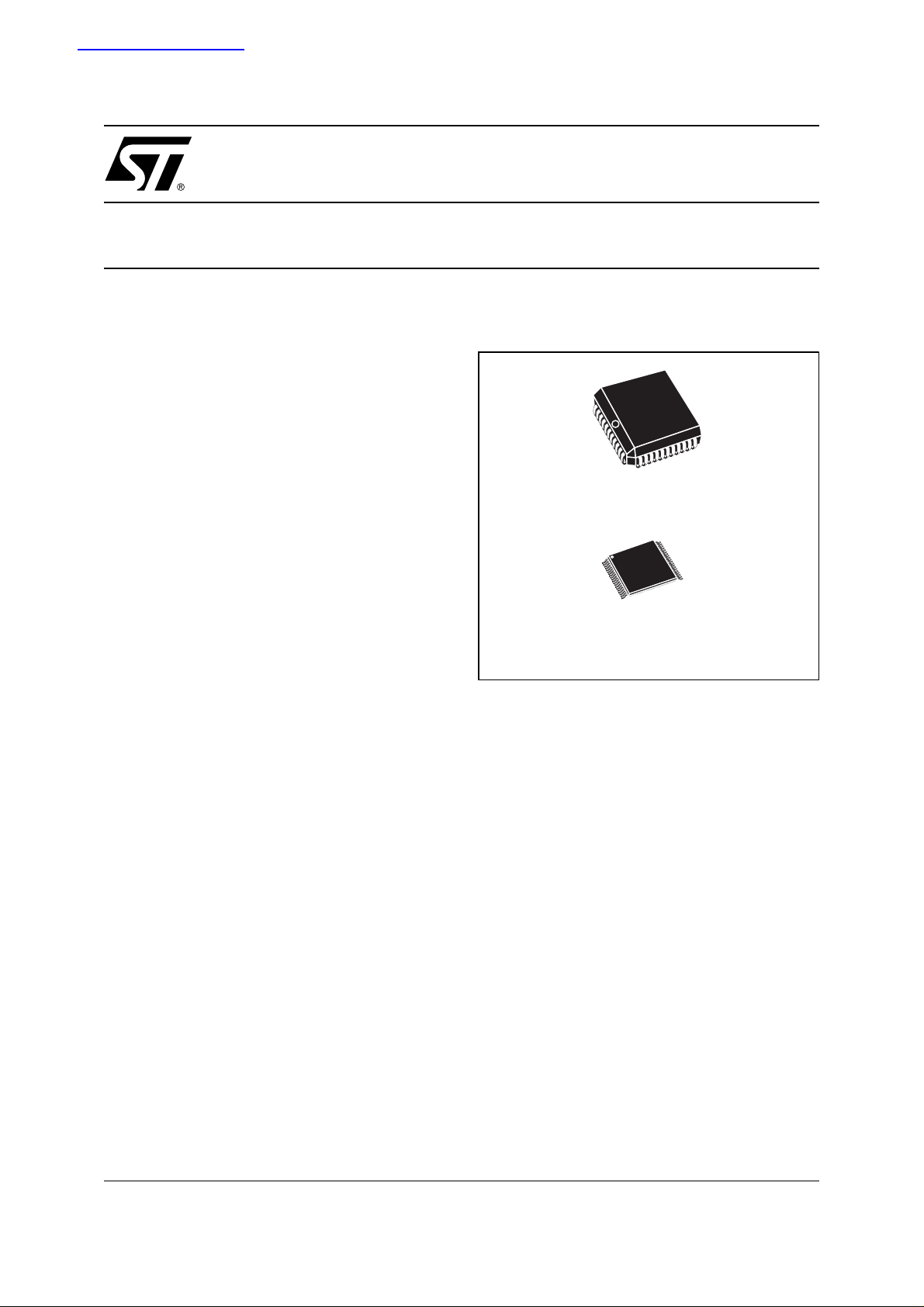
Figure 1. Package
PLCC44 (K)
TSOP40 (N)
10 x 14mm
1/24November 2004
Page 2

M29F102BB
TABLE OF CONTENTS
FEATURES SUMMARY . . . . . . . . . . . . . . . . . . . . . . . . . . . . . . . . . . . . . . . . . . . . . . . . . . . . . . . . . . . . . 1
Figure 1. Package. . . . . . . . . . . . . . . . . . . . . . . . . . . . . . . . . . . . . . . . . . . . . . . . . . . . . . . . . . . . . . . 1
SUMMARY DESCRIPTION. . . . . . . . . . . . . . . . . . . . . . . . . . . . . . . . . . . . . . . . . . . . . . . . . . . . . . . . . . . 4
Figure 2. Logic Diagram . . . . . . . . . . . . . . . . . . . . . . . . . . . . . . . . . . . . . . . . . . . . . . . . . . . . . . . . . . 4
Table 1. Signal Names . . . . . . . . . . . . . . . . . . . . . . . . . . . . . . . . . . . . . . . . . . . . . . . . . . . . . . . . . . 4
Table 2. Bottom Boot Block Addresses, M29F102BB . . . . . . . . . . . . . . . . . . . . . . . . . . . . . . . . . . . 4
Figure 3. PLCC Connections . . . . . . . . . . . . . . . . . . . . . . . . . . . . . . . . . . . . . . . . . . . . . . . . . . . . . . 5
Figure 4. TSOP Connections . . . . . . . . . . . . . . . . . . . . . . . . . . . . . . . . . . . . . . . . . . . . . . . . . . . . . . 5
SIGNAL DESCRIPTIONS . . . . . . . . . . . . . . . . . . . . . . . . . . . . . . . . . . . . . . . . . . . . . . . . . . . . . . . . . . . . 6
Address Inputs (A0-A15). . . . . . . . . . . . . . . . . . . . . . . . . . . . . . . . . . . . . . . . . . . . . . . . . . . . . . . . . . 6
Data Inputs/Outputs (DQ0-DQ15). . . . . . . . . . . . . . . . . . . . . . . . . . . . . . . . . . . . . . . . . . . . . . . . . . . 6
Chip Enable (E
Output Enable (G
Write Enable (W
Reset/Block Temporary Unprotect (RP
V
Supply Voltage. . . . . . . . . . . . . . . . . . . . . . . . . . . . . . . . . . . . . . . . . . . . . . . . . . . . . . . . . . . . . . 6
CC
Vss Ground.. . . . . . . . . . . . . . . . . . . . . . . . . . . . . . . . . . . . . . . . . . . . . . . . . . . . . . . . . . . . . . . . . . . . 6
). . . . . . . . . . . . . . . . . . . . . . . . . . . . . . . . . . . . . . . . . . . . . . . . . . . . . . . . . . . . . . . . . 6
). . . . . . . . . . . . . . . . . . . . . . . . . . . . . . . . . . . . . . . . . . . . . . . . . . . . . . . . . . . . . . . 6
). . . . . . . . . . . . . . . . . . . . . . . . . . . . . . . . . . . . . . . . . . . . . . . . . . . . . . . . . . . . . . . .6
).. . . . . . . . . . . . . . . . . . . . . . . . . . . . . . . . . . . . . . . . . . . . . . 6
BUS OPERATIONS. . . . . . . . . . . . . . . . . . . . . . . . . . . . . . . . . . . . . . . . . . . . . . . . . . . . . . . . . . . . . . . . . 7
Bus Read. . . . . . . . . . . . . . . . . . . . . . . . . . . . . . . . . . . . . . . . . . . . . . . . . . . . . . . . . . . . . . . . . . . . . . 7
Bus Write. . . . . . . . . . . . . . . . . . . . . . . . . . . . . . . . . . . . . . . . . . . . . . . . . . . . . . . . . . . . . . . . . . . . . . 7
Output Disable. . . . . . . . . . . . . . . . . . . . . . . . . . . . . . . . . . . . . . . . . . . . . . . . . . . . . . . . . . . . . . . . . . 7
Standby. . . . . . . . . . . . . . . . . . . . . . . . . . . . . . . . . . . . . . . . . . . . . . . . . . . . . . . . . . . . . . . . . . . . . . . 7
Automatic Standby. . . . . . . . . . . . . . . . . . . . . . . . . . . . . . . . . . . . . . . . . . . . . . . . . . . . . . . . . . . . . . . 7
Special Bus Operations . . . . . . . . . . . . . . . . . . . . . . . . . . . . . . . . . . . . . . . . . . . . . . . . . . . . . . . . . 7
Electronic Signature. . . . . . . . . . . . . . . . . . . . . . . . . . . . . . . . . . . . . . . . . . . . . . . . . . . . . . . . . . . . . . 7
Block Protection and Blocks Unprotection. . . . . . . . . . . . . . . . . . . . . . . . . . . . . . . . . . . . . . . . . . . . .7
Table 3. Bus Operations . . . . . . . . . . . . . . . . . . . . . . . . . . . . . . . . . . . . . . . . . . . . . . . . . . . . . . . . . 7
COMMAND INTERFACE . . . . . . . . . . . . . . . . . . . . . . . . . . . . . . . . . . . . . . . . . . . . . . . . . . . . . . . . . . . . 8
Read/Reset Command. . . . . . . . . . . . . . . . . . . . . . . . . . . . . . . . . . . . . . . . . . . . . . . . . . . . . . . . . . . . 8
Auto Select Command. . . . . . . . . . . . . . . . . . . . . . . . . . . . . . . . . . . . . . . . . . . . . . . . . . . . . . . . . . . . 8
Program Command. . . . . . . . . . . . . . . . . . . . . . . . . . . . . . . . . . . . . . . . . . . . . . . . . . . . . . . . . . . . . . 8
Unlock Bypass Command. . . . . . . . . . . . . . . . . . . . . . . . . . . . . . . . . . . . . . . . . . . . . . . . . . . . . . . . . 8
Unlock Bypass Program Command. . . . . . . . . . . . . . . . . . . . . . . . . . . . . . . . . . . . . . . . . . . . . . . . . . 8
Unlock Bypass Reset Command. . . . . . . . . . . . . . . . . . . . . . . . . . . . . . . . . . . . . . . . . . . . . . . . . . . . 8
Chip Erase Command. . . . . . . . . . . . . . . . . . . . . . . . . . . . . . . . . . . . . . . . . . . . . . . . . . . . . . . . . . . . 9
Block Erase Command.. . . . . . . . . . . . . . . . . . . . . . . . . . . . . . . . . . . . . . . . . . . . . . . . . . . . . . . . . . . 9
Erase Suspend Command. . . . . . . . . . . . . . . . . . . . . . . . . . . . . . . . . . . . . . . . . . . . . . . . . . . . . . . . . 9
Erase Resume Command. . . . . . . . . . . . . . . . . . . . . . . . . . . . . . . . . . . . . . . . . . . . . . . . . . . . . . . . . 9
Table 4. Commands . . . . . . . . . . . . . . . . . . . . . . . . . . . . . . . . . . . . . . . . . . . . . . . . . . . . . . . . . . . 10
2/24
Page 3

M29F102BB
Table 5. Program, Erase Times and Program, Erase Endurance Cycles (TA = 0 to 70°C). . . . . . 10
STATUS REGISTER . . . . . . . . . . . . . . . . . . . . . . . . . . . . . . . . . . . . . . . . . . . . . . . . . . . . . . . . . . . . . . . 11
Data Polling Bit (DQ7). . . . . . . . . . . . . . . . . . . . . . . . . . . . . . . . . . . . . . . . . . . . . . . . . . . . . . . . . . . 11
Toggle Bit (DQ6).. . . . . . . . . . . . . . . . . . . . . . . . . . . . . . . . . . . . . . . . . . . . . . . . . . . . . . . . . . . . . . . 11
Error Bit (DQ5). . . . . . . . . . . . . . . . . . . . . . . . . . . . . . . . . . . . . . . . . . . . . . . . . . . . . . . . . . . . . . . . . 11
Erase Timer Bit (DQ3). . . . . . . . . . . . . . . . . . . . . . . . . . . . . . . . . . . . . . . . . . . . . . . . . . . . . . . . . . . 11
Alternative Toggle Bit (DQ2).. . . . . . . . . . . . . . . . . . . . . . . . . . . . . . . . . . . . . . . . . . . . . . . . . . . . . . 11
Table 6. Status Register Bits . . . . . . . . . . . . . . . . . . . . . . . . . . . . . . . . . . . . . . . . . . . . . . . . . . . . . 12
Figure 5. Data Polling Flowchart. . . . . . . . . . . . . . . . . . . . . . . . . . . . . . . . . . . . . . . . . . . . . . . . . . . 12
Figure 6. Data Toggle Flowchart. . . . . . . . . . . . . . . . . . . . . . . . . . . . . . . . . . . . . . . . . . . . . . . . . . . 12
MAXIMUM RATINGS . . . . . . . . . . . . . . . . . . . . . . . . . . . . . . . . . . . . . . . . . . . . . . . . . . . . . . . . . . . . . . 13
Table 7. Absolute Maximum Ratings (1) . . . . . . . . . . . . . . . . . . . . . . . . . . . . . . . . . . . . . . . . . . . . 13
DC AND AC PARAMETERS. . . . . . . . . . . . . . . . . . . . . . . . . . . . . . . . . . . . . . . . . . . . . . . . . . . . . . . . . 14
Table 8. Operating and AC Measurement Conditions. . . . . . . . . . . . . . . . . . . . . . . . . . . . . . . . . . 14
Figure 7. AC Testing Input Output Waveform. . . . . . . . . . . . . . . . . . . . . . . . . . . . . . . . . . . . . . . . . 14
Figure 8. AC Testing Load Circuit. . . . . . . . . . . . . . . . . . . . . . . . . . . . . . . . . . . . . . . . . . . . . . . . . . 14
Table 9. Capacitance (TA = 25 °C, f = 1 MHz) . . . . . . . . . . . . . . . . . . . . . . . . . . . . . . . . . . . . . . . 14
Table 10. DC Characteristics (T
Table 11. Read AC Characteristics (TA = 0 to 70°C) . . . . . . . . . . . . . . . . . . . . . . . . . . . . . . . . . . . 16
Figure 9. Read Mode AC Waveforms. . . . . . . . . . . . . . . . . . . . . . . . . . . . . . . . . . . . . . . . . . . . . . . 16
Table 12. Write AC Characteristics, Write Enable Controlled (TA = 0 to 70 °C) . . . . . . . . . . . . . . . 17
Figure 10.Write AC Waveforms, Write Enable Controlled. . . . . . . . . . . . . . . . . . . . . . . . . . . . . . . . 17
Table 13. Write AC Characteristics, Chip Enable Controlled (TA = 0 to 70 °C) . . . . . . . . . . . . . . . 18
Figure 11.Write AC Waveforms, Chip Enable Controlled . . . . . . . . . . . . . . . . . . . . . . . . . . . . . . . . 18
Table 14. Reset/Block Temporary Unprotect AC Characteristics (T
Figure 12.Reset/Block Temporary Unprotect AC Waveforms. . . . . . . . . . . . . . . . . . . . . . . . . . . . . 19
= 0 to 70°C) . . . . . . . . . . . . . . . . . . . . . . . . . . . . . . . . . . . . . . . . 15
A
= 0 to 70°C). . . . . . . . . . . . . 19
A
PACKAGE MECHANICAL . . . . . . . . . . . . . . . . . . . . . . . . . . . . . . . . . . . . . . . . . . . . . . . . . . . . . . . . . . 20
Figure 13.PLCC44 - 44 lead Plastic Leaded Chip Carrier, Package Outline . . . . . . . . . . . . . . . . . 20
Table 15. PLCC44 - 44 lead Plastic Leaded Chip Carrier, Package Mechanical Data . . . . . . . . . . 20
Figure 14.TSOP40 - 40 lead Plastic Thin Small Outline, 10 x 14mm, Package Outline . . . . . . . . . 21
Table 16. PTSOP40 - 40 lead Plastic Thin Small Outline, 10 x 14mm, Package Mechanical Data 21
ORDERING INFORMATION SCHEME. . . . . . . . . . . . . . . . . . . . . . . . . . . . . . . . . . . . . . . . . . . . . . . . . 22
Table 17. Ordering Information Scheme . . . . . . . . . . . . . . . . . . . . . . . . . . . . . . . . . . . . . . . . . . . . . 22
REVISION HISTORY. . . . . . . . . . . . . . . . . . . . . . . . . . . . . . . . . . . . . . . . . . . . . . . . . . . . . . . . . . . . . . . 23
Table 18. Revision History. . . . . . . . . . . . . . . . . . . . . . . . . . . . . . . . . . . . . . . . . . . . . . . . . . . . . . . . 23
3/24
Page 4

M29F102BB
SUMMARY DESCRIPTION
The M29F102BB is a 1 Mbit (64Kb x16) non-volatile memory that c an be read, erased and r eprogrammed. These operations can be performed
using a single 5V supply. On power-up the memory defaults to i ts R ead m ode wh er e it c an b e re ad
in the same way as a ROM or EPROM.
The memory is divided into blocks that can be
erased independently s o i t is po ss ible to preserve
valid data while old data is erased. Each block can
be protected independen tly to prevent accidental
Program or Erase com mands from modifying the
memory. Program and Erase co mmands are written to the Command Int erface of the memo ry. An
on-chip Program/Erase Controller simplifies the
process of programming or erasing the memory by
taking care of all of the special operations that are
required to update the memory contents. The end
of a program or erase operation ca n be detected
and any error conditions ide nti fie d. T he co mma nd
set required to control the memory is consistent
with JEDEC standards.
The blocks in the memo ry are asymmet rically arranged, see Table 2., Bottom Boot Block Address-
es, M29F102BB. Th e first 32 Kwords have been
divided into four additional blocks. The 8 Kword
Boot Block can be used for small initialization code
to start the microproces sor, the two 4 Kword Parameter Blocks can be used for parameter storage
and the remaining 16 Kwords are a small Main
Block where the application may be stored.
Chip Enable, Output Enable and Write Enable signals control the bus operation of the memory.
They allow simple connection to most microprocessors, often without additional logic.
The memory is offered in PLCC44 and TSOP40
(10 x 14mm) packages. In addition to the standard
version, the packages are also avail able in Leadfree version, in compliance with JEDEC Std JSTD-020B, the ST ECOPACK 7191395 Specification, and the RoHS (Restriction of Hazardous Substances) di rective. A ll package s are compli ant with
Lead-free soldering processes.
The memory is supplied with all the bits erased
(set to ’1’).
Figure 2. Logic Diagram
V
CC
16
A0-A15
W
E
G
RP
M29F102BB
V
SS
Table 1. Signal Names
A0-A15 Address Inputs
DQ0-DQ15 Data Inputs/Outputs
E
G
W
RP
V
CC
V
SS
NC Not Connected Inter na lly
Chip Enable
Output Enable
Write Enable
Reset/Block Temporary Unprotect
Supply Voltage
Ground
16
DQ0-DQ15
AI02130C
Table 2. Bottom Boot Block Addresses, M29F102BB
# Size (KWords) Address Range
4 32 8000h-FFFFh
3 16 4000h-7FFFh
2 4 3000h-3FFFh
1 4 2000h-2FFFh
0 8 0000h-1FFFh
4/24
Page 5

Figure 3. PLCC Connections Figure 4. TSOP Connections
M29F102BB
DQ12
DQ11
DQ10
DQ9
DQ8
V
SS
NC
DQ6
DQ5
DQ4
12
DQ13
DQ14
DQ3
DQ2
DQ15
RP
E
M29F102BB
23
G
DQ1
DQ0
A9
A10
CC
W
V
NC
44
1
NC
A15
A14
34
A13
A12
A11
A10
A9
V
SS
NC
A8DQ7
A7
A6
A5
A11
A12
A13
A14
A15
NC
V
CC
RP
DQ15
DQ14
DQ13
DQ12
A3
NC
A0
A1
A2
A4
AI02131C
DQ11
DQ10
DQ9
DQ8
1
W
10
M29F102BB
11
E
20 21
40
31
30
AI02132C
V
SS
A8
A7
A6
A5
A4
A3
A2
A1
A0
G
DQ0
DQ1
DQ2
DQ3
DQ4
DQ5
DQ6
DQ7
V
SS
5/24
Page 6

M29F102BB
SIGNAL DESCRIPTIONS
See Figure 2., Logic Diagram, and Table
1., Signal Names, for a brief overview of the sig-
nals connected to this device.
Address Inputs (A0-A15). The Address Inputs
select the cells in the memory array to access during Bus Read operations. During Bus Write operations they control the commands sent to the
Command Interface of the internal state machine.
Data Inputs/Outputs (DQ0-DQ15). The Data Inputs/Outputs output the data stored at the selected
address during a Bus Read operation. During Bus
Write operations DQ0-DQ7 represent the commands sent to the Command Interface of the internal state machine; the Comma nd Interface does
not use DQ8-DQ15 to decode the commands.
Chip Enable (E
the memory, allowing Bus Read and Bus Write operations to be performed. When Chip Enable is
High, V
IH
Output Enable (G
trols the Bus Read operation of the memory.
Write Enable (W
the Bus Write operation of the memory’s Command Interface.
Reset/Block Temporary Un protect (RP
set/Block Temporary Unprotect pin can be used to
apply a Hardware Reset to the memory or to temporarily unprotect al l blocks that have been protected.
A Hardware Reset is achieved by holding Reset/
Block Temporary Unp rotect Low, V
. After Reset/Block Temporary Unprotect
t
PLPX
goes High, V
). The Chip Enable, E, activates
, all other pins are ignored.
). The Output Enable, G, con-
). The Write Enabl e, W, controls
IL
, the memory will be ready fo r Bus
IH
). The Re-
, for at least
Read and Bus Write operations after t
or t
, whichever occurs last. See Table
PLYH
PHEL
13., Write AC Characteristics, Chip Enable Controlled (TA = 0 to 70 °C) and Figure 12., Reset/
Block Temporary Unprotect AC Waveforms.
Holding RP
at VID will temporarily unprotect the
protected blocks in the memory. Program and
Erase operations on all blocks will be possible.
The transition from V
t
PHPHH
.
to VID must be slower than
IH
Reset/Block Temporary Unprotect can be left unconnected. A weak internal pull-up resistor ensures that the memory always operates correctly.
Supply Voltage. The VCC Supply Voltage
V
CC
supplies the power for all operations (Read, Program, Erase etc.).
The Command Interface is disabled when the V
CC
Supply Voltage is le ss than the Lockout Vo ltage,
. This prevents Bus Write operations from ac-
V
LKO
cidentally damaging the data during power up,
power down and power surges. If the Program/
Erase Controller is programming or erasing during
this time then the operation aborts and the memory contents being altered will be invalid.
A 0.1µF capacito r should be connected between
the V
Supply Voltage pin and the VSS Ground
CC
pin to decouple the current surges from the power
supply. The PCB track widths must be sufficient to
carry the currents required during program and
erase operations, I
Vss Ground. The V
.
CC3
Ground is the reference
SS
for all voltage measurements.
6/24
Page 7
BUS OPERATIONS
There are five standard bus operations that control
the device. These are Bus Read, Bus Writ e, Output Disable, Standby and Automatic Standby. See
Table 3., Bus Operations, for a summary. Ty pi cal-
ly glitches of less than 5ns on Chip Enable or Write
Enable are ignored by the m emo ry and do not affect bus operations.
Bus Read. Bus Read operations read from the
memory cells, or specific registers in the Command Interface. A valid Bus Read operation involves setting the desired address on the Address
Inputs, applying a Low s ig nal, V
and Output Enable and keeping Write Enable
High, V
. The Data Inputs/Outputs will ou tpu t the
IH
value, see Figure 9., Read Mode AC Wavefor ms,
and Table 11., Read AC Characteristics (TA = 0 to
70°C), for details of wh en t he o utpu t be comes val-
id.
Bus Write. Bus Write operations write to the
Command Interface. A v alid Bus Write operati on
begins by setting the desired address on the Address Inputs. The Ad dress Inputs are latched b y
the Command Interface on the falling edge of Chip
Enable or Write Enable, whichever occurs last.
The Data Inputs/Outputs ar e latched by the Com mand Interface on the rising ed ge of Chip Enab le
or Write Enable, whichever occurs first. Output Enable must remain High, V
IH
Write operation. See Figures 10 and 11, Write AC
Waveforms, and Tables 12 and 13, Write AC
Characteristics, for details of the timing requirements.
Output Disable. The Data Inputs/Outpu ts are in
the high impedance state when Output Enable is
High, V
.
IH
Standby. When Chip Enable is High, V
memory enters Standby mode and the Data Inputs/Outputs pins are placed in the high-impedance state. To reduce the Su pply Current to the
, to Chip Enable
IL
, during the whole Bus
, the
IH
M29F102BB
Standby Supply Current, I
be held within V
± 0.2V. For the Standby current
CC
level see Table 10., DC Characteristics (T
70°C).
During program or eras e operations the memory
will continue to use the Program/Erase Supply
Current, I
, for Program or Erase operations un-
CC3
til the operation completes.
Automatic Standby. If CMOS levels (V
are used to drive the bus and the bus is inactive for
150ns or more the memory enters Automatic
Standby where the interna l Supply Current is reduced to the Standby Supply Current, I
Data Inputs/Outputs will still output data if a Bus
Read operation is in progress.
Special Bus Operations
Additional bus operations can be performed to
read the Electronic Signature and also to apply
and remove Block Protection. These bus operations are intended for us e by progr ammin g equip ment and are not usually used in applications.
They require V
to be applied to some pins.
ID
Electronic Signature. The memory has two
codes, the manufacturer code and the device
code, that can be read to identify the memory.
These codes can b e read b y apply ing the sig nals
listed in Table 3., Bus Operat ion s.
Block Protection and Blocks Unprotection. Each
block can be separately protected against accidental Program or Erase. Protected blocks can be
unprotected to allow data to be changed.
There are two methods available for protecting
and unprotecting the b locks, one for use on programming equipment and t he other for in-system
use. For further information refer to Application
Note AN1122, Applying Protectio n and Unpr otection to M29 Series Flash.
, Chip Enable should
CC2
CC
CC2
= 0 to
A
± 0.2V)
. The
Table 3. Bus Operations
Operation E G W Address Inputs
Bus Read
Bus Write
Output Disable X
Standby
Read Manufacturer
Code
Read Device Code
Note: 1. X = VIL or VIH.
Data
Inputs/Outputs
V
IL
V
IL
V
IH
V
IL
V
IL
V
IL
V
IH
V
IH
X X X Hi-Z
V
IL
V
IL
V
V
V
V
V
Cell Address Data Output
IH
Command Address Data Input
IL
X Hi-Z
IH
A0 = VIL, A1 = VIL, A9 = VID,
IH
Others V
A0 = VIH, A1 = VIL, A9 = VID,
IH
Others V
IL
IL
or V
or V
IH
IH
0020h
0097h
7/24
Page 8

M29F102BB
COMMAND INTERFACE
All Bus Write operations to the memory are interpreted by the Command Interface. Commands
consist of one or more sequential Bus Write operations. Failure to observe a valid sequence of Bus
Write operation s will result in the memory return ing to Read mode. The long command sequences
are imposed to maximize data security.
The commands are summarized in Table
4., Commands. Refer to Table 4. in conjunction
with the text descriptions below.
Read/Reset Command. The Read/Reset com-
mand returns the memory to its Read mode where
it behaves lik e a ROM or EPROM. I t also resets
the errors in the Status Register. Either one or
three Bus Write o perations can be us ed to issue
the Read/Reset command.
If the Read/Reset command is issued during a
Block Erase operation or following a Programming
or Erase error then the memory will take up to 10
to abort. During the abort period no valid data can
be read from the memory. Issu ing a Read/Reset
command during a Block Erase operation will
leave invalid data in the memory.
Auto Select Command. The Auto Select command is used to read t he Manu facturer Code, the
Device Code and the Block Protection Status.
Three consecutive Bus Write operations are required to issue the Auto Sel ect command. Once
the Auto Select comman d is issued the memory
remains in Auto Sele ct mode until another command is issued.
From the Auto Select mode the Manufacturer
Code can be read using a Bus Read operation
with A0 = V
may be set to either V
and A1 = VIL. The other address bits
IL
or VIH. The Manufacturer
IL
Code for STMicroelectronics is 0020h.
The Device Code ca n be read using a Bu s Read
operation with A0 = V
address bits may be s et to either V
and A1 = VIL. The other
IH
or VIH. The
IL
Device Code for the M29F102BB is 0097h.
The Block Protectio n Statu s of ea ch block c an be
read using a Bus Read ope ration with A0 = V
A1 = V
, and A12-A15 s pecifying the addr ess of
IH
the block. The other address bits may be set to either V
or VIH. If the addressed block is protected
IL
then 01h is output on Data Inputs/Outputs
DQ0-DQ7, otherwise 00h is output.
Program Command. The Program command
can be used to program a value to one address in
the memory array at a time. The command requires four Bus Write operations, the final write operation latches the address and data in the internal
state machine and starts the Program/Erase Controller.
µs
IL
If the address falls in a protect ed block then the
Program command is ignored, the data remains
unchanged. The Status Register is never read and
no error condition is given.
During the program operation th e memory will ig nore all commands. It is no t possib le to is sue any
command to abort or pause the operation. Typical
program times are given in Table 5.. Bus Read operations during the p rogram operation will output
the Status Register on the Data Inputs/Outputs.
See the section on the Status Register for more
details.
After the program operation has completed the
memory will return to the Read mode, unless an
error has occurred. When an error occurs the
memory will continue to output the Statu s Register. A Read/Reset command must be issued to reset the error condition and return to Read mode.
Note that the Program command cannot change a
bit set at ’0’ back t o ’1’. One of the Erase Commands must be used to set all the bits in a block or
in the whole memory from ’0’ to ’1’.
Unlock Bypass Command. The Unlock Bypass
command is used in conjunction with the Unlock
Bypass Program command to program the memory. When the access time to the device is long (as
with some EPROM programmers) considerable
time saving can be made by using these commands. Three Bu s Write operations are r equired
to issue the Unlock Bypass command.
Once the Unlock Bypass c ommand has been issued the memory will only accept the Unlock Bypass Program com mand and the Unlock B ypass
Reset command. The memory can be read as if in
Read mode.
Unlock Bypass Program Command. The Unlock Bypass Program command can be used to
program one address in memory at a time. The
command requires t wo Bus Write oper ations, the
final write operati on lat ches the a ddress and d ata
in the internal state machine and starts the Program/Erase Controller.
,
The Program operation us ing the Unlock Bypass
Program command behaves identically to the Program operation using the Program command. A
protected block cannot be progra mme d; the op eration cannot be aborted and the Status Register is
read. Errors must be reset using th e Read/Reset
command, which leav es the device in Unlock Bypass Mode. See the Program command for details
on the behavior.
Unlock Bypass Reset Command. The Unlock
Bypass Reset comm and can b e used to return to
Read/Reset mode from Unlock Bypass Mode.
Two Bus Write operations are required to issue the
Unlock Bypass Reset command.
8/24
Page 9

M29F102BB
Chip Erase Command. The Chip Erase com-
mand can be used to erase the entire chip. Six Bus
Write operations are required to issue the Chip
Erase Command and start the Program/Erase
Controller.
If any blocks are protected then these are ignored
and all the other blocks are erased. If all of the
blocks are protected the Chip Erase operation appears to start but will terminate within about 100µs,
leaving the data unc hanged . No er ror con dition is
given when protected blocks are ignored.
During the erase operation the memory will ignore
all commands. It is not possible to issue any command to abort the operation. Typical chip erase
times are given in T able 5.. All Bus Read operations during the Chip Erase operation will output
the Status Register on the Data Inputs/Outputs.
See the section on the Status Register for more
details.
After the Chip Erase o per at ion has c om ple ted the
memory will return to the Read Mode, unless an
error has occurred. When an error occurs the
memory will continue to output the Statu s Register. A Read/Reset command must be issued to reset the error condition and return to Read Mode.
The Chip Erase Command sets all of the bits in unprotected blocks of the memory to ’1’. All previous
data is lost.
Block Erase Command. The Block Erase command can be used to erase a l ist of one or more
blocks. Six Bus W rite operations are required to
select the first block in the list. Each additional
block in the list can be select ed by repeating the
sixth Bus Write operation using the address of the
additional block. The Bl ock Er as e op erati on starts
the Program/Erase Controller about 50µs after the
last Bus Write operation. Once the Program/Erase
Controller starts it is not possible to select any
more blocks. Each additional block must therefore
be selected within 50µs of the last block. The 50µs
timer restarts when an additional block is selected.
The Status Register can be read after the sixth
Bus Write operation. See the Status Register for
details on how to identify if the Program/Erase
Controller has started the Block Erase operation.
If any selected blocks are protected then these are
ignored and all the other selected blocks are
erased. If all of the sel ected blocks are pr otected
the Block Erase operation appears to start but will
terminate within about 100µs, leaving the data un-
changed. No error condition is given when protected blocks are ignored.
During the Block Eras e o perat ion the memory will
ignore all comman ds except the Erase Suspe nd
and Read/Reset commands . Typical block erase
times are given in Tab le 5.. All Bus Read operations during the B lock Erase op eration wil l output
the Status Register on the Data Inputs/Outputs.
See the section on the Status Register for more
details.
After the Block Erase operation has completed the
memory will return to the Read Mode, unless an
error has occurred. When an error occurs the
memory will continue to output the Statu s Register. A Read/Reset command must be issued to reset the error condition and return to Read mode.
The Block Erase Comma nd sets all of the bits in
the unprotected selected blocks to ’1’. All previous
data in the selected blocks is lost.
Erase Suspend Command. The Erase Suspend
Command may be used to tempor arily suspend a
Block Erase operatio n and return the memory to
Read mode. The command requires one Bus
Write operation.
The Program/Erase Control ler will sus pend with in
15µs of the E rase Suspend Command being issued. Once the Program/Erase Controller has
stopped the memory will be set to Read mode and
the Erase will be suspended. If the Erase Suspend
command is issued during the period when the
memory is waiting for an additiona l block (before
the Program/Erase Controller starts) then the
Erase is suspende d i mme di atel y and will start immediately when the Eras e Resume Command is
issued. It will not be possib le to select an y further
blocks for erasure after the Erase Resume.
During Erase Suspend i t is possible to Read and
Program cells in blocks that are not being erased;
both Read and Program operations behave as
normal on these bloc ks. Re adi ng fro m b lock s t hat
are being erased will output the Status Register. It
is also possible to enter the Auto Select mode: the
memory wil l behav e as in t he Auto Select mo de on
all blocks until a Read/Reset command returns the
memory to Erase Suspend mode.
Erase Resume Command. The Erase Resume
command must be used to restart the Program/
Erase Controller from Erase Suspend. An erase
can be suspended and resumed more than once.
9/24
Page 10

M29F102BB
Table 4. Commands
Bus Write Operations
Command
1X F0
Read/Reset
3555 AA2AA 55 X F0
Auto Select 3 555 AA 2AA 55 555 90
Program 4 555 AA 2AA 55 555 A0 PA PD
Unlock Bypass 3 555 AA 2AA 55 555 20
Unlock Bypass
Program
2 X A0 PA PD
Unlock Bypass Reset 2 X 90 X 00
Chip Erase 6 555 AA 2AA 55 555 80 555 AA 2AA 55 555 10
Block Erase 6+ 555 AA 2AA 55 555 80 555 AA 2AA 55 BA 30
Erase Suspend 1 X B0
Erase Resume 1 X 30
Note: 1. X Don’t Care, PA Program Address, PD Program Data, BA Any address in the Block.
2. All values in the table are in hexadecimal.
3. The Command Interface only uses address bits A0-A10 and DQ0-DQ7 to verify the commands, the upper address bits and the
upper data bits are Don’t Care.
4. Read/Reset.
5. After a Read/Reset command, read the memory as normal until another command is issued.
6. Auto Select.
7. After an Auto Select command, read Manufacturer ID, Device ID or Block Protection Status.
8. Program, Unlock Bypass Program, Chip Erase, Block Erase.
9. After these commands read the Status Register until the Program/Erase Controller completes and the memory returns to Read
Mode. Add additional Blocks during Block Erase Command with additional Bus Write Operations until t he Timeout Bit is set.
10. Unlock Bypass.
11. After the Unlock Bypass command iss ue Unlock Bypass Program or Unlock Bypass Reset commands.
12. Unlock Bypass Reset.
13. After the Unlock Bypass Reset comman d read the memory as normal until another command is issued.
14. Erase Suspend.
15. After the Erase Suspend comma nd read non- erasing memory blocks as normal, issue Auto Select and Progr am commands on nonerasing blocks as normal.
16. E rase Resume.
17. After the Erase Resume command the suspended Erase operation resumes, read the St atus Register until the Pro gram/Erase Controller completes and the memory returns to Read Mode.
1st 2nd 3rd 4th 5th 6th
Length
Addr Data Addr Data Addr Data Addr Data Addr Data Addr Data
Table 5. Program, Erase Times and Program, Erase Endurance Cycles (TA = 0 to 70°C)
Parameter Min
Typ
(1)
Chip Erase (All bits in the memory set to ‘0’) 0.6 0.6 s
Chip Erase 1.3 1.3 6 s
Block Erase (32 KWords) 0.6 0.6 4 s
Program 8 8 150 µs
Chip Program 0.6 0.6 2.5 s
Program/Erase Cycles (per Block) 100,000 cycles
Note: 1. TA = 25°C, VCC = 5V.
10/24
Typical after
100k W/E Cycles
(1)
Max Unit
Page 11

STATUS REGISTER
Bus Read operations from any address always
read the Status Register during Program and
Erase operations. It is also read during Erase Suspend when an address within a block being erased
is accessed.
The bits in the Status R egi st er are s umm ar iz ed in
Table 6., Status Register Bits.
Data Polling Bit (DQ7). The Da ta Poll ing Bit c an
be used to identify whether the Program/Erase
Controller has successfully completed its operation or if it has respond ed to an Erase Suspend.
The Data Polling Bit is output on DQ7 whe n the
Status Register is read.
During Program operations the Data Polling Bit
outputs the complement of the bit being programmed to DQ7. After successful completion of
the Program operation the memory returns to
Read mode and Bus Read operations from the address just programm ed output DQ7, not its complement.
During Erase operations the Data Polli ng Bit outputs ’0’, the complement of the erased state of
DQ7. After su ccess ful co mpl etion of t he Er ase o peration the memory returns to Read Mode.
In Erase Suspend mode the Data Polli ng Bit will
output a ’1’ during a Bus Rea d operation withi n a
block being erased. The Data Polling Bit will
change from a ’0’ to a ’1’ when the Program/Erase
Controller has suspended the Erase operation.
Figure 5., Data Polli ng Flowcha rt, give s an ex am-
ple of how to use the Data Po lli ng Bit . A Va li d Ad dress is the address being programmed or an
address within the block being erased.
Toggle Bit (DQ6). The Toggle Bit can be used to
identify whether the Program/Erase Controller has
successfully completed its operation or if it has responded to an Erase Suspend. The To ggle Bit is
output on DQ6 when the Status Register is read.
During Program and Er ase oper ations the Togg le
Bit changes from ’0’ to ’1 ’ to ’0’, etc., with succes sive Bus Read operations at any address. After
successful completion of the operation the memory returns to Read mode.
During Erase Suspend mode the Toggle Bit will
output when addressing a cell within a block being
erased. The Toggle Bit will stop toggling when the
Program/Erase Controller has suspended the
Erase operation.
Figure 6., Data Togg le F lo wch ar t, g iv es an exam -
ple of how to use the Data Toggle Bit.
M29F102BB
Error Bit (DQ5). The Error Bit can be used to
identify errors detected by the Program/Erase
Controller. The Error Bit is set to ’1’ when a Program, Block Erase or Chip Erase operation fails to
write the correct data to the memory. If the Error
Bit is set a Read/Reset command mus t be issu ed
before other comma nds are issued. The Error bit
is output on DQ5 when the Status Register is read.
Note that the Program command cannot change a
bit set at ’0’ back to ’1’ and attempting to do so may
or may not set DQ5 at ‘1’. I n both cases, a su ccessive Bus Read operation will show the bit is still ‘0’.
One of the Erase comma nds m ust b e use d to s et
all the bits in a block or in the whole memory from
’0’ to ’1’.
Erase Timer Bi t (DQ3). The Erase Timer B it can
be used to identify the start of Program/Erase
Controller operation during a Block Erase command. Once the Program/Erase Controller starts
erasing the Erase Timer Bit is set to ’1’. Before the
Program/Erase Cont roller starts the Erase Timer
Bit is set to ’0’ and additiona l blocks t o be erased
may be written to the Command Interface. The
Erase Timer Bit is output on DQ3 when the Status
Register is read.
Alternative Toggle Bit (DQ2). The Alternative
Toggle Bit can be u sed to monitor the Program/
Erase controller d uring Eras e operations. The Alternative Toggle Bit is output on DQ2 when the
Status Register is read.
During Chip Erase and Block Erase operations the
Toggle Bit changes from ’0 ’ to ’1’ to ’0’, etc., wi th
successive Bus Rea d operations from ad dresses
within the blocks being erased. Once the operation
completes the memory returns to Read mode.
During Erase Suspend the Alternative Toggle Bit
changes from ’0’ to ’1’ to ’0’, etc. with successive
Bus Read operations from addresses within the
blocks being erased . Bus Read operations to addresses within blocks not b ei ng e rase d wi ll output
the memory cell data as if in Read mode.
After an Erase o per at ion th at ca us es th e Er ror B it
to be set the Alternative Toggle Bit can be used to
identify which block or blocks have caused the error. The Alternative Toggle Bit changes from ’0’ to
’1’ to ’0’, etc. with successive Bus Read Operations from addresses with in blocks that have not
erased correctly. Th e Alternative Toggle B it does
not change if the addressed block has erased correctly.
11/24
Page 12

M29F102BB
Table 6. Status Register Bits
Operation Address DQ7 DQ6 DQ5 DQ3 DQ2
Program Any Address DQ7
Program During Erase Suspend Any Address DQ7
Program Error Any Address DQ7
Chip Erase Any Address 0 Toggle 0 1 Toggle
Erasing Block 0 Toggle 0 0 Toggle
Block Erase before timeout
Non-Erasing Block 0 Toggle 0 0 No To gg le
Erasing Block 0 Toggle 0 1 Toggle
Block Erase
Non-Erasing Block 0 Toggle 0 1 No To gg le
Erasing Block 1 No Toggle 0 – Toggle
Erase Suspend
Non-Erasing Block Data read as normal
Good Block Address 0 Toggle 1 1 No Toggle
Erase Error
Faulty Block Address 0 Toggle 1 1 Toggle
Note: 1. Unspecified data bits should be ignored.
Figure 5. Data Polling Flowchart Figure 6. Data Toggle Flowchart
Toggle 0 – –
Toggle 0 – –
Toggle 1 – –
START
READ DQ5 & DQ7
at VALID ADDRESS
DQ7
DATA
NO
DQ5
READ DQ7
at VALID ADDRESS
DQ7
DATA
FAIL PASS
= 1
YES
=
NO
YES
YES
=
NO
AI03598
START
READ
DQ5 & DQ6
READ DQ6
DQ6
=
TOGGLE
YES
NO
DQ5
= 1
YES
READ DQ6
TWICE
DQ6
=
TOGGLE
YES
FAIL PASS
NO
NO
AI01370B
12/24
Page 13

MAXIMUM RATINGS
Stressing the device above the ra ting l isted in the
Absolute Maximum Ratin gs table ma y cause per manent damage to the device. Expos ure to Ab so lute Maximum Rating conditions for extended
periods may affect device reliability. These are
stress ratings only and operation of th e device at
M29F102BB
these or any other conditions above those indicated in the Operating sections of this specification is
not implied. Refer also to the STMicroelectronics
SURE Program and o ther relevant quality documents.
Table 7. Absolute Maximum Ratings
(1)
Symbol Parameter Value Unit
T
A
T
BIAS
T
STG
T
LEAD
(2)
V
IO
V
CC
V
ID
Note: 1. Except for the rating "Operating Temperature Range", stresses above those listed in Table 7. ,Absolute Max imum Rat ings (1 ) may
cause permanent damage to the device. Thes e are str ess ratin gs only and oper at ion of the device at thes e or any ot her condi tio ns
above those indicated in the Operating sections of this specification is not implied. Exposure to Absolute Maximum Rating conditions for extended periods may affect dev ice reliability. Refer also to the S TMicroelectronics SURE Progr am and other relevant quality documents.
2. Minimum Voltage may undershoot to –2V during transition and for less than 20ns during transitions.
3. Compliant with the JEDEC Std J-STD-020B (for small body, Sn-Pb or Pb assembly), the ST ECOPACK
and the European directive on Restr i ctions on Hazardous Substances (RoHS) 2002/95/EU.
Ambient Operatin g Temperature 0 to 70 °C
Temperature Under Bias –50 to 125 °C
Storage Temperature –65 to 150 °C
Lead Temperature during Soldering
(3)
Input or Output Voltage –0.6 to 6 V
Supply Voltage –0.6 to 6 V
Identification Voltage –0.6 to 13.5 V
®
7191395 specification,
13/24
Page 14

M29F102BB
DC AND AC PARAMETERS
This section summ arizes the operating measurement conditions, and th e DC and AC c haracteris tics of the device. The parameters in the DC and
AC characteristics Tables that follow, are derived
from tests performed under the Measurement
Table 8. Operating and AC Measurement Conditions
Parameter
Conditions summarized in Table 9, Operating and
AC Measurement Conditions. Designers should
check that the operating conditi ons in their circuit
match the operating conditions when relying on
the quoted parameters.
M29F102BB Unit
Min Max
Load Capacitance (C
)
L
30 pF
Input Rise and Fall Times 10 ns
Input Pulse Voltages 0 3 V
Input and Output Timing Ref. Voltages 1.5 V
Figure 7. AC Testing Input Output Waveform Figure 8. AC Testing Load Circuit
1.3V
3V
0V
1.5V
AI01417
DEVICE
UNDER
TEST
CL includes JIG capacitance
1N914
3.3kΩ
CL = 30pF
OUT
AI02979
Table 9. Capacitance (T
= 25 °C, f = 1 MHz)
A
Symbol Parame te r Test Condition Min Max Unit
V
V
IN
OUT
= 0V
= 0V
6pF
12 pF
C
IN
C
OUT
Note: Sampled only, not 100% tested.
Input Capacitance
Output Capacitance
14/24
Page 15

Table 10. DC Characteristics (TA = 0 to 70°C)
Symbol Parameter Test Condition Min
I
LI
I
LR1
I
LR2
I
I
CC1
I
CC2
LO
(1)
Input Leakage Current
RP Leakage Current High
RP Leakage Current Low
Output Leakage Current
Supply Current (Read)
Supply Current (Standby)
0V ≤ V
0V ≤ V
E
= VIL, G = VIH, f = 6MHz
E
≤ V
IN
CC
RP
= V
CC
RP
= V
SS
≤ V
OUT
= VCC ±0.2V,
CC
RP = VCC ±0.2V
M29F102BB
(3)
Typ
–0.2 –10 µA
620mA
30 100 µA
Max Unit
±1 µA
±1 µA
±1 µA
CC3
V
V
V
V
OH
V
I
ID
V
LKO
Note: 1. Excluding the RP input.
2. Sampled only, not 100% tested.
3. T
Erase)
Input Low Voltage –0.5 0.8 V
IL
Input High Voltage 2
IH
Output Low Voltage
OL
Output High Voltage
Identification Voltage 11.5 12.5 V
ID
Identification Current
Program/Erase Lockout
(2)
Supply Voltage
= 25°C, VCC = 5V
A
Supply Current (Program/
(2)
I
Program/Erase
Controller active
I
= 5.8mA
OL
I
= –100µA VCC –0.4
OH
A9 = V
ID
20 mA
V
+0.5
CC
0.45 V
100 µA
3.2 4.2 V
V
V
15/24
Page 16

M29F102BB
Table 11. Read AC Characteristics (TA = 0 to 70°C)
Symbol Alt Parameter Test Condition
35 45 5 0 / 55 70
= VIL,
(1)
t
AVAV
(1)
t
AVQV
(2)
t
ELQX
(1)
t
ELQV
(2)
t
GLQX
(1)
t
GLQV
(2)
t
EHQZ
(2)
t
GHQZ
t
EHQX
t
GHQX
t
AXQX
Note: 1. This timing refers to a Load Capacitance (CL) of 30pF. If CL is higher, add 1.5ns for each extra 10pF .
2. Sampled only, not 100% tested.
Address Valid to Next Address
t
RC
Valid
t
Address Valid to Output Valid
ACC
Chip Enable Low to Output
t
LZ
Transition
t
Chip Enable Low to Output Valid
CE
Output Enable Low to Output
t
OLZ
Transition
Output Enable Low to Output
t
OE
Valid
t
Chip Enable High to Output Hi-Z
HZ
Output Enable High to Output Hi-
t
DF
Z
Chip Enable, Output Enable or
t
Address Transition to Output
OH
Transition
E
G
= V
E
= VIL,
G
= V
= V
G
G
= V
= V
E
= V
E
G
= V
= V
E
Min35455070ns
IL
Max35455070ns
IL
Min0000ns
IL
Max35455070ns
IL
Min0000ns
IL
Max20202030ns
IL
Max15151820ns
IL
Max15151820ns
IL
Min0000ns
M29F102BB
Unit
Figure 9. Read Mode AC Waveforms
A0-A15
tAVQV tAXQX
E
G
DQ0-DQ15
tAVAV
VALID
tELQV
tELQX tEHQZ
tGLQX tGHQX
tGLQV
tGHQZ
VALID
tEHQX
AI02980
16/24
Page 17

Table 12. Write AC Characteristics, Write Enable Controlled (TA = 0 to 70 °C)
Symbol Alt Parameter
t
AVAV
t
ELWL
t
WLWH
t
DVWH
t
WHDX
t
WHEH
t
WHWL
t
AVWL
t
WLAX
t
GHWL
t
WHGL
t
VCHEL
t
Address Valid to Next Address Valid Min 35 45 50 70 ns
WC
t
Chip Enable Low to Write Enable LowMin0000ns
CS
t
Write Enable Low to Write Enable High Min 35 40 40 45 ns
WP
t
Input Valid to Write Enab le High Min 20 25 25 30 ns
DS
t
Write Enable High to Input TransitionMin0000ns
DH
t
Write Enable High to Chip Enable HighMin0000ns
CH
t
Write Enable High to Write Enable Low Min 20 20 20 20 ns
WPH
t
Address Valid to Write Enable Low Min0000ns
AS
t
Write Enable Low to Address Transition Min 35 40 40 45 ns
AH
Output Enable High to Write Enable LowMin0000ns
t
Write Enable High to Output Enable LowMin0000ns
OEH
t
VCSVCC
High to Chip Enable Low
35 45 50 / 55 70
Min50505050µs
M29F102BB
M29F102BB
Unit
Figure 10. Write AC Waveforms, Write Enable Controlled
tAVAV
A0-A15
E
G
W
DQ0-DQ15
V
CC
tAVWL
tELWL
tVCHEL
VALID
tWLWHtGHWL
tDVWH
tWLAX
tWHEH
tWHGL
tWHWL
tWHDX
VALID
AI02119
17/24
Page 18

M29F102BB
Table 13. Write AC Characteristics, Chip Enable Controlled (TA = 0 to 70 °C)
Symbol Alt Parameter
t
AVAV
t
WLEL
t
ELEH
t
DVEH
t
EHDX
t
EHWH
t
EHEL
t
AVEL
t
ELAX
t
GHEL
t
EHGL
t
VCHWL
t
Address Valid to Next Address Valid Min 35 45 50 70 ns
WC
t
Write Enable Low to Chip Enable LowMin0000ns
WS
t
Chip Enable Low to Chip Enable High Min 35 40 40 45 ns
CP
t
Input Valid to Chip Enable High Min 20 25 25 30 ns
DS
t
Chip Enable High to Input TransitionMin0000ns
DH
t
Chip Enable High to Write Enable HighMin0000ns
WH
t
Chip Enable High to Chip Enable Low Min 20 20 20 20 ns
CPH
t
Address Valid to Chip Enable Low Min0000ns
AS
t
Chip Enable Low to Address Transition Min 35 40 40 45 ns
AH
Output Enable High Chip Enable LowMin0000ns
t
Chip Enable High to Output Enable LowMin0000ns
OEH
t
VCSVCC
High to Write Enable Low
35 45 50 / 55 70
Min50505050µs
M29F102BB
Unit
Figure 11. Write AC Waveforms, Chip Enable Controlled
tAVAV
A0-A15
W
G
E
DQ0-DQ15
V
CC
tAVEL
tWLEL
tVCHWL
VALID
tELEHtGHEL
tDVEH
tELAX
tEHWH
tEHGL
tEHEL
tEHDX
VALID
AI02120
18/24
Page 19

Table 14. Reset/Block Temporary Unprotect AC Characteristics (TA = 0 to 70°C)
Symbol Alt Parameter
(1)
t
PHWL
t
PHEL
(1)
t
PHGL
t
PLPX
(1)
t
PLYH
(1)
t
PHPHH
Note: 1. Sampled only, not 100% tested.
t
t
t
READY
t
VIDR
RP High to Write Enable Low, Chip Enable
RH
Low, Output Enable Low
RP Pulse Width Min 500 500 500 ns
RP
RP Low to Read Mode Max 10 10 10 µs
RP Rise Time to V
ID
Min505050ns
Min 500 500 500 ns
M29F102BB
50 70 90
Figure 12. Reset/Block Temporary Unprotect AC Waveforms
E, G
W,
tPHWL, tPHEL, tPHGL
RP
tPLPX
tPHPHH
tPLYH
M29F102BB
Unit
AI02943
19/24
Page 20

M29F102BB
PACKAGE MECHANICAL
Figure 13. PLCC44 - 44 lead Plastic Leaded Chip Carrier, Package Outline
E3
Note: Drawing is not to scale.
D
D1
1 N
E1 E
D3
D2
E2
A1
c
B1
e
B
A2
A
CP
PLCC-B
Table 15. PLCC44 - 44 lead Plastic Leaded Chip Carrier, Package Mechanical Data
Symbol
Typ Min Max Typ Min Max
A 4.200 4.570 0.1654 0.1799
A1 2.290 3.040 0.0902 0.1197
A2 3.650 3.700 0.1437 0.1457
B 0.331 0.533 0.0130 0.0210
B1 0.661 0.812 0.0260 0.0320
CP 0.101 0.0040
c 0.510 0.0201
D 17.400 17.650 0.6850 0.6949
D1 16.510 16.662 0.6500 0.6560
D2 14.990 16.000 0.5902 0.6299
D3 12.700 – – 0.5000 – –
E 17.400 17.650 0.6850 0.6949
E1 16.510 16.660 0.6500 0.6559
E2 14.990 16.000 0.5902 0.6299
E3 12.700 – – 0.5000 – –
e 1.270 – – 0.0500 – –
N44 44
millimeters inches
20/24
Page 21

Figure 14. TSOP40 - 40 lead Plastic Thin Small Outline, 10 x 14mm, Package Outline
A2
1 N
e
E
B
N/2
M29F102BB
D1
D
DIE
A
CP
C
TSOP-a
Note: Drawing is not to scale.
LA1 α
Table 16. PTSOP40 - 40 lead Plastic Thin Small Outline, 10 x 14mm, Package Mechanical Data
Symbol
Typ Min Max Typ Min Max
A1.200.0472
A1 0.05 0.15 0.0020 0.0059
A2 0.95 1.05 0.0374 0.0413
B 0.17 0.27 0.0067 0.0106
C 0.10 0.21 0.0039 0.0083
D 13.80 14.20 0.5433 0.5591
D1 12.30 12.50 0.4843 0.4921
E 9.90 10.10 0.3898 0.3976
e 0.50 – – 0.0197 – –
L 0.50 0.70 0.0197 0.0276
α 0° 5° 0° 5°
N40 40
CP 0.10 0.0039
millimeters inches
21/24
Page 22

M29F102BB
ORDERING INFORMATION SCHEME
Table 17. Ordering Information Scheme
Example: M29F102BB 50 N 1 T
Device Type
M29
Operating Voltage
F = VCC = 5V ± 10%
Device Function
102BB = 1 Mbit (64Kb x16), Bottom Boot Block
Speed
35 = 35ns
45 = 45 ns
50 = 50 ns
55 = 55 ns
70 = 70 ns
Package
K = PLCC44
N = TSOP40:10 x 14mm
Temperature Range
1 = 0 to 70 °C
Option
T = Tape & Reel Packing
F = Lead-free and RoHS Package, Tape & Reel Packing
Note: The last two characters of th e ordering cod e may be r eplaced by a letter code for preprogr ammed
parts, otherwise devices are shipped from the factory with the memory content bits erased to ‘1’.
For a list of avai la ble opt ion s (Spe ed, Pac k age , et c... ) or for fu r ther i nfo rm ati on o n a ny aspec t o f th is de vice, please contact the ST Sales Office nearest to you.
22/24
Page 23

REVISION HISTORY
Table 18. Revision History
Date Version Revision Details
July 1999 1.0 First Issue
New document template
28-Jul-00 2.0
30-Nov-2004 3.0
Status Register bit DQ5 clarification
Data Polling Flowchart diagram change (Figure 5.)
Data Toggle Flowchart diagram change ( Figure 6.)
Document restructured.
PLCC44 and TSOP40 Lead-free options added: SUMMARY DESCRIPTION, SIGNAL
DESCRIPTIONS updated with Lead-free packages, T
7., Absolute Maximum Ratings (1) and Lead-free option added in Table 17., Ordering
Information Scheme.
parameter added in Table
LEAD
M29F102BB
23/24
Page 24

M29F102BB
Information furnished is be lieved to be a ccur ate and reli able. Howe ver, STMicroele ctronic s assu mes no r esponsib ilit y for th e consequences
of use of such information nor for any infrin gement of patent s or other rights of third parties which ma y result from it s use. No license is granted
by implication or otherwi se under any patent or patent rig hts of STMicroelectronics. Specifica tions mentioned in this publication are subject
to change without not ice. This pub licat ion su persed es and repl aces all in format ion previou sly su pplie d. STMicroele c tronic s prod ucts ar e no t
authorized for use as critical compone nts in life support devices or systems without exp ress written approval of STMicroelectronics.
The ST logo is a registered trademark of STMicroelectronics.
ECOPACK is a registered trademark of STMicroelectronics.
All other names are the property of their respective owners
© 2004 STMicroelectronics - All rights reserved
Australia - Belgium - Brazil - Canada - China - Czech Republic - Finland - France - Germany - Hong Kong - India - Israel - It aly - Japan -
Malaysia - Malta - Morocco - Singapore - Spain - Sweden - Switzerland - United Kingdom - United States of America
STMicroelectronics group of companies
www.st.com
24/24
 Loading...