

Page 1
1 Mbit (128Kb x8 or 64Kb x16, Boot Block)
5V ± 10% SUPPLYVOLTAGEfor PROGRAM,
ERASEand READOPERATIONS
FASTACCESSTIME: 70ns
FASTPROGRAMMING TIME
–10µs by Byte / 16µs by Word typical
PROGRAM/ERASE CONTROLLER(P/E.C.)
– Program Byte-by-Byteor Word-by-Word
– StatusRegister bits and Ready/Busy Output
MEMORYBLOCKS
– Boot Block (Top or Bottom location)
– Parameterand Main blocks
BLOCK, MULTI-BLOCKand CHIPERASE
MULTI-BLOCKPROTECTION/TEMPORARY
UNPROTECTION MODES
ERASESUSPEND and RESUMEMODES
– Read and Program anotherBlockduring
Erase Suspend
LOW POWER CONSUMPTION
– Stand-byand Automatic Stand-by
100,000 PROGRAM/ERASECYCLESper
BLOCK
20 YEARSDATARETENTION
– Defectivity below 1ppm/year
ELECTRONICSIGNATURE
– ManufacturerCode: 0020h
– Device Code, M29F100T:00D0h
– Device Code, M29F100B:00D1h
DESCRIPTION
The M29F100 is a non-volatile memory that may
beerasedelectricallyat theblock or chiplevel and
programmedin-systemona Byte-by-Byteor Wordby-Word basis using only a single 5V V
For Program and Erase operations the necessary
high voltages are generatedinternally. The device
can also be programmed in standard programmers.
Thearraymatrixorganisationallowseach blockto
be erased and reprogrammed without affecting
otherblocks. Blockscan be protectedagainst programing and erase on programming equipment,
and temporarily unprotected to make changes in
the application. Each block can be programmed
and erased over100,000 cycles.
CC
supply.
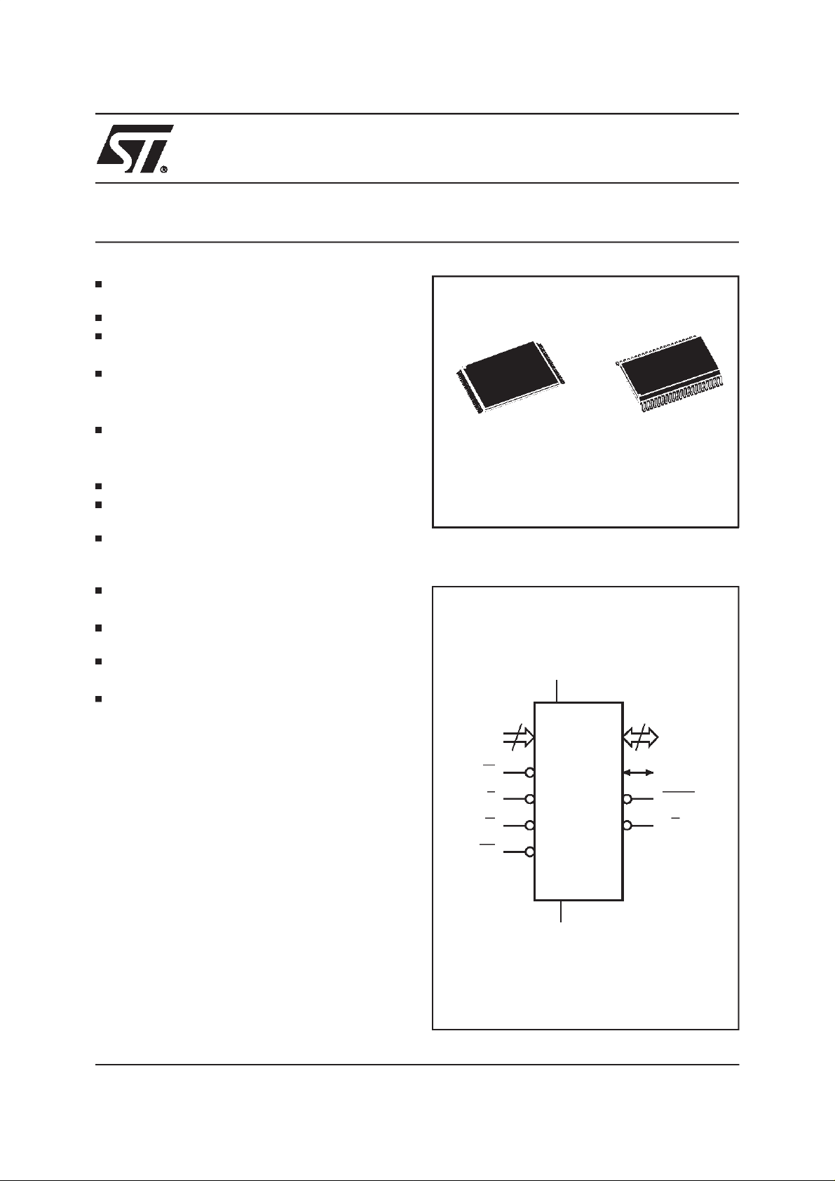
M29F100T
M29F100B
Single Supply Flash Memory
44
1
12 x 20 mm
Figure1. LogicDiagram
V
CC
16
A0-A15
W
E
G
RP
M29F100T
M29F100B
V
SS
SO44 (M)TSOP48 (N)
15
DQ0-DQ14
DQ15A–1
BYTE
RB
AI01974
July 1998 1/30
Page 2
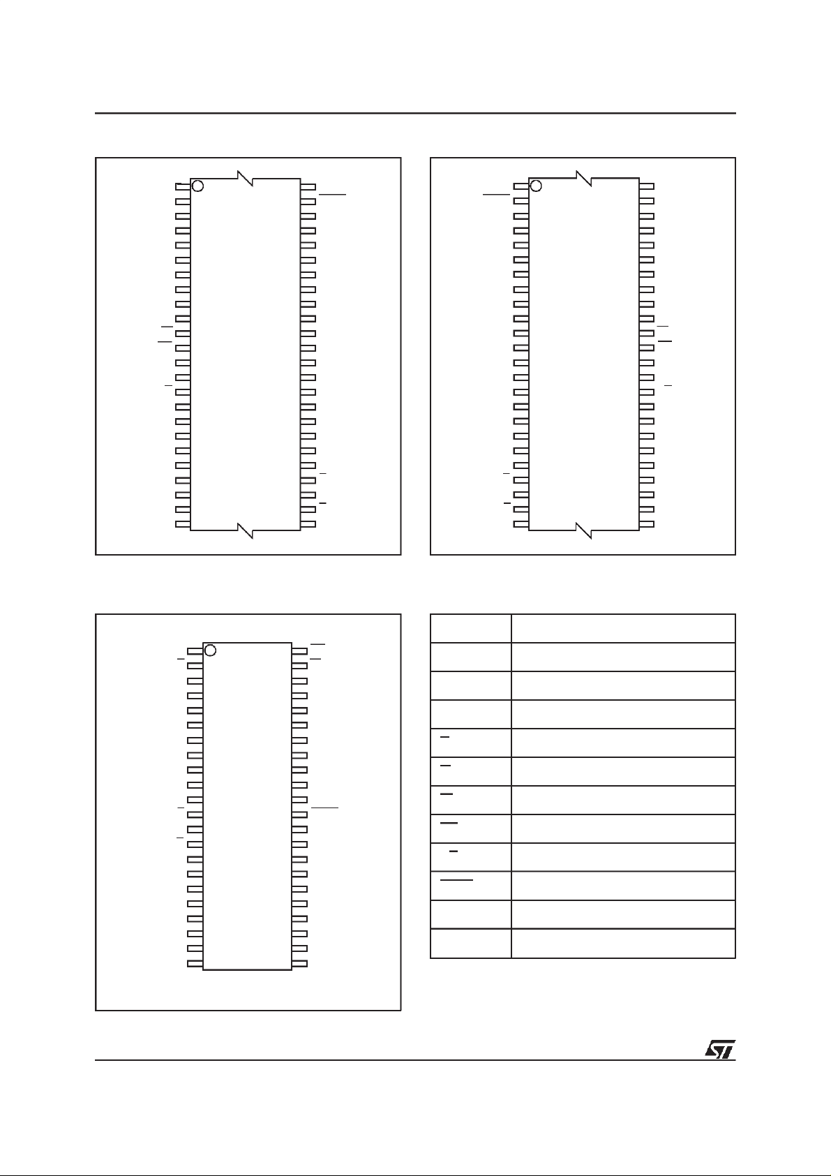
M29F100T, M29F100B
Figure2A. TSOPPin Connections
A15
1
A14
A13
A12
A11
A10 DQ14
A9
A8
NC
NC
W
RP
NC
NC
RB
NC
NC
A7
A6
A5
A4
A3
A2
A1
M29F100T
12
M29F100B
13
(Normal)
24 25
48
37
36
AI01975
NC
BYTE
V
SS
DQ15A–1
DQ7
DQ6
DQ13
DQ5
DQ12
DQ4
V
CC
DQ11
DQ3
DQ10
DQ2
DQ9
DQ1
DQ8
DQ0
G
V
SS
E
A0
Figure2B. TSOPReverse PinConnections
NC
BYTE
V
SS
DQ15A–1
DQ7
DQ14
DQ6
DQ13
DQ5
DQ12
DQ4
V
CC
DQ11
DQ3
DQ10
DQ2
DQ9
DQ1
DQ8
DQ0
V
SS
A0
1
M29F100T
12
M29F100B
13
(Reverse)
G
E
24 25
AI01976
48
37
36
A15
A14
A13
A12
A11
A10
A9
A8
NC
NC
W
RP
NC
NC
RB
NC
NC
A7
A6
A5
A4
A3
A2
A1
Warning: NC = Not Connected. Warning: NC = Not Connected.
Figure2C. SO Pin Connections
Table 1. Signal Names
A0-A15 Address Inputs
NC RP
1
2
3
NC A8
A7
4
5
A6
6
A5
A4
7
A3
8
A2
9
A1
10
A0
11
M29F100T
M29F100B
12
13
14
15
16
17DQ1
18
19
20
21
V
SS
DQ0
DQ8
DQ9
DQ10
DQ3
DQ11
E
G
44
43
42
41
40
39
38
37
36
35
34
33
32
31
30
29
28
27
26
25
24
2322
AI01977
WRB
A9
A10
A11
A12
A13
A14
A15
NC
BYTE
V
SS
DQ15A–1
DQ7
DQ14
DQ6
DQ13
DQ5DQ2
DQ12
DQ4
V
CC
DQ0-DQ7 Data Input/Outputs, Command Inputs
DQ8-DQ14 Data Input/Outputs
DQ15A–1 Data Input/Outputor AddressInput
E Chip Enable
G Output Enable
W Write Enable
RP Reset / Block TemporaryUnprotect
RB Ready/Busy Output
BYTE Byte/Word Organisation
V
CC
V
SS
Supply Voltage
Ground
Warning: NC = Not Connected.
2/30
Page 3
M29F100T, M29F100B
Table 2. Absolute Maximum Ratings
Symbol Parameter Value Unit
T
A
T
BIAS
T
STG
(2)
V
IO
V
CC
V
(A9, E, G, RP)
Notes: 1. Except for therating ”Operating Temperature Range”, stressesabove those listedin theTable ”AbsoluteMaximum Ratings”
may cause permanent damage to thedevice. These are stress ratings only and operation of the device at these or any other
conditions above those indicated in the Operatingsections of this specification is not implied.Exposure to Absolute Maximum
Rating conditions for extended periods may affectdevice reliability.Refer also tothe STMicroelectronics SURE Programand other
relevant quality documents.
2. Minimum Voltagemay undershoot to –2V during transitionand for less than 20ns.
3. Depends on range.
Ambient Operating Temperature
Temperature Under Bias –50 to 125
Storage Temperature –65 to 150
Input or Output Voltages –0.6to 7 V
Supply Voltage –0.6to 7 V
(2)
A9, E, G, RP Voltage –0.6to 13.5 V
DESCRIPTION(Cont’d)
Instructionsfor Read/Reset, Auto Select for read-
ing the Electronic Signature or Block Protection
status,Programming,BlockandChipErase,Erase
Suspend and Resume are written to the device in
cyclesofcommandstoa CommandInterfaceusing
standardmicroprocessorwrite timings.
Thedevice is offered in TSOP48(12 x 20mm)and
SO44packages.Both normal and reversepinouts
are available for the TSOP48package.
Organisation
The M29F100 is organisedas 128Kb x8 or 64Kb
x16 bits selectable by the BYTE signal. When
BYTE is Low the Byte-wide x8 organisation is
selectedand the address lines are DQ15A–1and
A0-A15. The Data Input/Outputsignal DQ15A–1
actsas addresslineA–1which selectsthe loweror
upper Byte of the memory word for output on
DQ0-DQ7,DQ8-DQ14remainat Highimpedance.
WhenBYTEis Highthe memoryusesthe address
inputs A0-A15 and the Data Input/Outputs DQ0DQ15.Memory controlisprovided by ChipEnable
E, OutputEnable G andWrite EnableW inputs.
AReset/BlockTemporaryUnprotection RPtri-level
input providesa hardware reset whenpulled Low,
andwhenheldHigh(atV
)temporarily unprotects
ID
blocks previously protected allowing them to be
programedanderased.EraseandProgramoperations are controlled by an internal Program/Erase
Controller(P/E.C.).StatusRegister data outputon
DQ7providesa Data Pollingsignal, and DQ6and
DQ2provideTogglesignals to indicatethe stateof
(1)
(3)
–40 to 125
C
°
C
°
C
°
the P/E.C operations. A Ready/Busy RB output
indicatesthe completionof theinternalalgorithms.
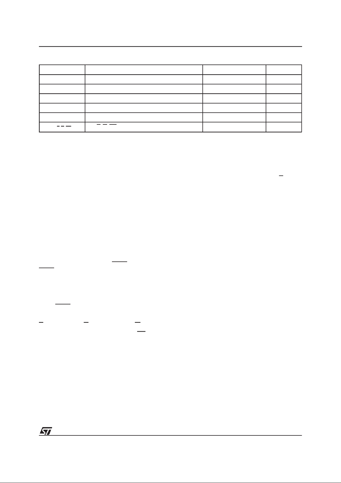
MemoryBlocks
Thedevicesfeatureasymmetrically blocked architectureprovidingsystemmemory integration.Both
M29F100Tand M29F100B devices have an array
of 5 blocks, one Boot Block of 16 KBytes or 8
KWords, two Parameter Blocks of 8 KBytes or 4
KWords, one Main Block of 32 KBytes or 16
KWordsand one Main Blocks of 64 KBytesor 32
KWords.TheM29F100Thas the Boot Blockat the
top of the memory add ress space and the
M29F100B locates the Boot Block starting at the
bottom. The memory maps are showed in Figure
3. Each block can be erased separately,any combination of blocks can be specified for multi-block
eraseor the entire chipmay beerased. The Erase
operations are managed automatically by the
P/E.C. The block erase operation can be suspended in order to read from or program to any
blocknot being ersased, and then resumed.
Block protection provides additional data security.
Each block can be separately protected or unprotectedagainst Program or Erase on programming
equipment.All previouslyprotected blocks can be
temporarilyunprotectedin the application.
Bus Operations
The following operations can be performed using
theappropriatebus cycles:Read(Array,Electronic
Signature, Block Protection Status), Write command, Output Disable,Standby,Reset, Block Protection, Unprotection, Protection Verify,
Unprotection Verify and Block Temporary Unprotection.See Tables4 and 5.
3/30
Page 4
M29F100T, M29F100B
Figure3. MemoryMap and Block Address Table(x8)
M29F100B
64K MAIN BLOCK
32K MAIN BLOCK
8K PARAMETER BLOCK
8K PARAMETER BLOCK
16K BOOT BLOCK
AI01978
1FFFFh
1C000h
1BFFFh
1A000h
19FFFh
18000h
17FFFh
10000h
0FFFFh
00000h
M29F100T
16K BOOTBLOCK
8K PARAMETER BLOCK
8K PARAMETER BLOCK
32K MAIN BLOCK
64K MAIN BLOCK
1FFFFh
10000h
0FFFFh
08000h
07FFFh
06000h
05FFFh
04000h
03FFFh
00000h
Table 3A. M29F100T Block AddressTable
Address Range (x8) Address Range (x16) A15 A14 A13 A12
00000h-0FFFFh 0000h-7FFFh 0 X X X
10000h-17FFFh 8000h-BFFFh 1 0 X X
18000h-19FFFh C000h-CFFFh 1 1 0 0
1A000h-1BFFFh D000h-DFFFh 1 1 0 1
1C000h-1FFFFh E000h-FFFFh 1 1 1 X
Table 3B. M29F100B BlockAddress Table
Address Range (x8) Address Range (x16) A15 A14 A13 A12
00000h-03FFFh 0000h-1FFFh 0 0 0 X
04000h-05FFFh 2000h-2FFFh 0 0 1 0
06000h-07FFFh 3000h-3FFFh 0 0 1 1
08000h-0FFFFh 4000h-7FFFh 0 1 X X
10000h-1FFFFh 8000h-FFFFh 1 X X X
4/30
Page 5

M29F100T, M29F100B
CommandInterface
Instructions,made up of commands written in cycles,can be givento theProgram/EraseController
through a Command Interface (C.I.). For added
dataprotection,program or erase executionstarts
after4 or 6 cycles.The first,second,fourthandfifth
cycles are used to input Coded cycles to the C.I.
This Coded sequence is the same for all Program/Erase Controller instructions. The ’Command’itself and its confirmation,when applicable,
are given on the third, fourth or sixth cycles. Any
incorrectcommand or any improper command sequencewill resetthe deviceto ReadArray mode.
Instructions
Seven instructions are defined to perform Read
Array, Auto Select(to readtheElectronicSignature
or BlockProtectionStatus),Program,Block Erase,
Chip Erase, Erase Suspend and Erase Resume.
The internal P/E.C. automatically handles all timing and verification of the Program and Erase
operations.The Status Register Data Polling, Toggle, Error bits and the RB output may be read at
anytime, duringprogramming or erase,to monitor
the progress of the operation.
Instructionsare composedof up to six cycles.The
first two cycles input a Coded sequence to the
CommandInterfacewhich iscommontoall instructions (see Table 8). The third cycle inputs the
instruction set-up command. Subsequent cycles
outputthe addressed data,ElectronicSignatureor
Block Protection Status for Read operations. In
orderto giveadditionaldataprotection,the instructionsfor Programand Blockor Chip Erase require
furthercommandinputs.ForaPrograminstruction,
the fourth command cycle inputs the address and
data to be programmed. For an Erase instruction
(Block or Chip), the fourth and fifth cycles input a
furtherCoded sequence before the Eraseconfirm
commandon thesixth cycle. Erasure of a memory
blockmaybesuspended,inordertoreaddatafrom
anotherblock or to programdata in anotherblock,
and then resumed.
When power is first applied or if V
, the command interface is reset to Read
V
LKO
falls below
CC
Array.
SIGNALDESCRIPTIONS
See Figure 1 and Table1.
AddressInputs (A0-A15).The addressinputs for
thememoryarrayarelatchedduringa write operation on the falling edge of Chip Enable E or Write
EnableW. In Word-wide organisationthe address
lines are A0-A15, in Byte-wide organisation
DQ15A–1acts as an additionalLSB address line.
WhenA9 is raisedto V
, eithera Read Electronic
ID
Signature Manufacturer or Device Code, Block
Protection Status or a Write Block Protection or
Block Unprotection is enabled depending on the
combinationof levelson A0,A1,A6, A12 and A15.
Data Input/Outputs (DQ0-DQ7). These Inputs/Outputsare used in theByte-wide and Wordwide organisat ions. The input is data to be
programmed in the memory array or a command
to be written to the C.I. Both are latched on the
rising edge of Chip Enable E or Write Enable W.
The output is data from the Memory Array, the
Electronic Signature Manufacturer or Device
codes, the Block Protection Status or the Status
registerData Polling bit DQ7, the Toggle Bits DQ6
and DQ2, the Errorbit DQ5 or the Erase Timer bit
DQ3. Outputs are valid when Chip Enable E and
Output Enable G are active. The output is high
impedance when the chip is deselected or the
outputsaredisabledandwhenRPis at aLowlevel.
Data Input/Outputs (DQ8-DQ14and DQ15A–1).
These Inputs/Outputsare additionally used in the
Word-wideorganisation.WhenBYTEis HighDQ8DQ14 and DQ15A–1 act as the MSB of the Data
Inputor Output,functioningas describedfor DQ0DQ7 above, and DQ8-DQ15 are ’don’t care’ for
commandinputs or statusoutputs. When BYTEis
Low,DQ8-DQ14are highimpedance,DQ15A–1is
theAddress A–1 input.
Chip Enable (E). The Chip Enable input activates
the memory control logic, input buffers, decoders
andsenseamplifiers.E Highdeselectsthememory
andreducesthepower consumptiontothestandby
level. E can also be used to control writing to the
commandregister and to the memory array,while
Wremainsat a low level.TheChip Enablemustbe
forcedto V
duringthe Block Unprotectionopera-
ID
tion.
OutputEnable (G). TheOutput Enable gates the
outputs through the data buffers during a read
operation. When G is High the outputs are High
impedance. G must be forced to V
level during
ID
BlockProtectionand Unprotection operations.
WriteEnable(W). This inputcontrols writingto the
CommandRegisterand Addressand Datalatches.
Byte/Word Organization Select (BYTE). The
BYTEinput selects the outputconfigurationfor the
device: Byte-wide (x8) mode or Word-wide (x16)
mode. When BYTEis Low,the Byte-widemode is
selectedand the data is read and programmedon
DQ0-DQ7. In this mode, DQ8-DQ14 are at high
impedance and DQ15A–1 is the LSB address.
When BYTE is High, the Word-wide mode is selected and the data is read and programmed on
DQ0-DQ15.
5/30
Page 6

M29F100T, M29F100B
Ready/Busy Output (RB). Ready/Busy is an
open-drainoutputandgivestheinternalstateof the
P/E.C. of the device.When RB is Low, the device
is Busy with a Program or Erase operation and it
will not accept any additional program or erase
instructionsexcept the Erase Suspendinstruction.
WhenRBis High,the deviceis readyforany Read,
Program or Erase operation. The RB will also be
Highwhen the memoryis putin EraseSuspendor
Standbymodes.
Reset/Block Temporary Unprotect Input (RP).
The RP Input provides hardware reset and protected block(s) temporary unprotection functions.
Reset of the memory is acheived by pullingRP to
for at least 500ns. When the reset pulse is
V
IL
given,if thememoryis in Read or Standbymodes,
it will be availablefor new operationsin 50nsafter
the rising edge of RP. If the memory is in Erase,
Erase Suspend or Program modes the reset will
take 10µs during which the RB signal will be held
.Theendof thememoryresetwillbeindicated
atV
IL
by the rising edge of RB. A hardware reset during
anEraseor Programoperationwillcorruptthe data
beingprogrammedor the sector(s)being erased.
Temporary block unprotection is made by holding
RP at V
. In this condition previously protected
ID
blockscan be programmed or erased. The transitionof RP fromV
When RP is returned from V
toVIDmust slowerthan500ns.
IH
to VIHall blocks
ID
temporarilyunprotectedwill be again protected.
V
Supply Voltage. The power supply for all
CC
operations(Read, Programand Erase).
V
Ground. VSSis the reference for all voltage
SS
measurements.
DEVICEOPERATIONS
See Tables 4, 5 and 6.
Read. Read operations are used to output the
contents of the Memory Array,the ElectronicSignature,theStatusRegisteror the BlockProtection
Status.Both Chip Enable E and Output Enable G
must be low in order to read the output of the
memory.
Write.Writeoperationsareused to giveInstruction
Commandsto thememoryor tolatch input datato
beprogrammed.Awrite operationisinitiatedwhen
Chip Enable E is Low and Write Enable W is Low
withOutput Enable G High.Addressesare latched
onthe fallingedge ofWorEwhicheveroccurslast.
CommandsandInputDataarelatchedontherising
edgeof W or E whichever occurs first.
OutputDisable.The dataoutputsare highimpedancewhen the OutputEnableG is High with Write
EnableW High.
Standby. The memory is in standby when Chip
EnableE is High and theP/E.C.is idle. Thepower
consumption is reduced to the standbylevel and
the outputs are high impedance, independent of
the Output Enable G or WriteEnable W inputs.
AutomaticStandby. After 150ns of bus inactivity
and when CMOS levels are drivingthe addresses,
the chip automatically enters a pseudo-standby
modewhere consumptionis reducedto the CMOS
standbyvalue, while outputsstill drive the bus.
ElectronicSignature. Two codes identifying the
manufacturer andthe devicecan bereadfrom the
memory. The manufacturer’s code for STMicroelectronicsis20h,the devicecodeis D0hfor the
M29F100T(Top Boot) and D1h forthe M29F100B
(Bottom Boot). These codes allow programming
equipment or applicationsto automatically match
their interface to the characteristics of the
M29F100.The ElectronicSignatureis output by a
Read operationwhen the voltageapplied to A9 is
and addressinput A1 is Low.The manufac-
at V
ID
turer code is output when the Address input A0 is
Low and the device code when this input is High.
Other Address inputs are ignored. The codes are
output on DQ0-DQ7.
TheElectronic Signaturecan alsobe read, without
raisingA9to V
, bygivingthe memorythe Instruc-
ID
tion AS. If the Byte-wide configuration is selected
thecodesare output onDQ0-DQ7withDQ8-DQ14
at High impedance; if the Word-wide configuration
isselectedthe codes are output onDQ0-DQ7with
DQ8-DQ15at 00h.
Block Protection. Each block can be separately
protected against Program or Erase on programming equipment. Block protection provides additional data security, as it disables all program or
eraseoperations.Thismodeis activatedwhenboth
A9 and G are raised to V
and an address in the
ID
blockis appliedon A12-A15.The BlockProtection
algorithmis showninFigure14. Blockprotectionis
initiatedon the edge of W falling to V
a delayof 100µs,the edge of W rising to V
. Thenafter
IL
IH
ends
theprotectionoperations.Blockprotectionverifyis
achievedby bringingG, E, A0andA6toV
, while W is atVIHandA9atVID. Underthese
toV
IH
andA1
IL
conditions,reading the data outputwill yield 01h if
the block defined by the inputs on A12-A15 is
protected.Any attempt to programor erase a protectedblock will be ignored by the device.
6/30
Page 7
M29F100T, M29F100B
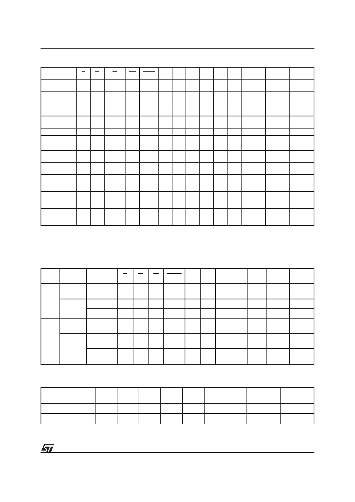
Table 4. User Bus Operations
(1)
Operation E G W RP BYTE A0 A1 A6 A9 A12 A15
Read Word V
Read Byte V
Write Word V
Write Byte V
Output Disable V
Standby V
ILVIL
ILVIL
ILVIH
ILVIH
ILVIH
IH
Reset X X X V
Block
Protection
Blocks
Unprotection
Block
Protection
Verify
Block
Unprotection
Verify
Block
Temporary
Unprotection
Notes: 1. X = V
(2,4) V
(2,4)
(2,4)
ILVIDVIL
(4)VIDVIDVIL
VILV
VILV
XX X V
or V
IL
2. Block Address must be given on A12-A15 bits.
3. See Table6.
4. Operation performed onprogramming equipment.
IH
V
V
V
IH
IH
V
V
IH
IH
V
V
IL
IH
V
V
IL
IH
V
V
IH
IH
A0 A1 A6 A9 A12 A15
IH
V
A0 A1 A6 A9 A12 A15
IL
V
A0 A1 A6 A9 A12 A15 Data Input Data Input
IH
V
A0 A1 A6 A9 A12 A15
IL
X X X X X X X Hi-Z Hi-Z Hi-Z
XXVIHX X X X X X X Hi-Z Hi-Z Hi-Z
X X X X X X X Hi-Z Hi-Z Hi-Z
IL
Pulse V
Pulse V
V
IL
IH
V
IL
IH
XXXXVIDXX X X X
IH
XXXXVIDVIHV
IH
V
XVILVIHVILVIDA12 A15 X X
IH
V
XVILVIHVIHVIDA12 A15 X X
IH
X XXXXXX X X X
ID
DQ15
A–1
Data
Output
Address
Input
Address
Input
XXX
IH
DQ8-
DQ14
Data
Output
Hi-Z
Hi-Z
DQ0-DQ7
Data
Output
Data
Output
Data
Input
Data
Input
Block
Protect
(3)
Status
Block
Protect
(3)
Status
Table 5. Read ElectronicSignature (followingAS instructionor with A9 = VID)
Org. Code Device E G W BYTE A0 A1
Word-
wide
Manufact.
Code
Device
Code
Manufact.
Code
M29F100T V
M29F100B V
V
VILV
IL
VILV
IL
VILV
IL
V
VILV
IL
V
IH
V
IH
V
IH
V
IH
VILVILDon’t Care 0 00h 20h
IH
V
IH
IH
IL
IH
V
IH
VILVILDon’t Care
Byte-
wide
Device
M29F100T V
IL
VILV
V
IH
V
IL
IH
Code
M29F100B V
IL
VILV
V
IH
V
IL
IH
Other
Addresses
VILDon’t Care 0 00h D0h
VILDon’t Care 0 00h D1h
VILDon’t Care
VILDon’t Care
DQ15
A–1
Don’t
Care
Don’t
Care
Don’t
Care
Table 6. Read Block Protectionwith AS Instruction
Code E G W A0 A1 A12 - A15
Protected Block V
Unprotected Block V
IL
IL
V
V
V
IL
IL
IH
V
IH
V
IL
V
IL
V
V
Block Address Don’t Care 01h
IH
Block Address Don’t Care 00h
IH
Addresses
Other
DQ8 DQ14
DQ0 -
DQ7
Hi-Z 20h
Hi-Z D0h
Hi-Z D1h
DQ0 - DQ7
7/30
Page 8
M29F100T, M29F100B
Block Temporary Unprotection. Any previously
protectedblock can be temporarilyunprotectedin
orderto changestoreddata.Thetemporaryunprotection mode is activated by bringing RP to V
ID
During the temporary unprotection mode the previously protected blocks are unprotected. A block
can be selected and data can be modified by
executingtheEraseorPrograminstructionwiththe
RPsignal heldat V
. When RPis returnedto VIH,
ID
all the previously protected blocks are again protected.
Block Unprotection. All protectedblocks can be
unprotected on programming equipmentto allow
updating of bit contents. All blocks must first be
protectedbefore the unprotectionoperation.Block
unprotectionis activated when A9, G and E are at
and A12, A15 at VIH. The Block Unprotection
V
ID
algorithm is shown in Figure 15. Unprotection is
initiatedbytheedgeofW fallingtoV
.Aftera delay
IL
of 10ms, the unprotection operation will end. Unprotectionverifyis achievedby bringingGand E to
whileA0 is at VIL, A6 and A1 are atVIHandA9
V
IL
remains at V
. In these conditions, reading the
ID
outputdata willyield 00h if theblock definedby the
inputsA12-A15hasbeen succesfullyunprotected.
Eachblock mustbeseparatelyverified bygivingits
address in order to ensure that it has beenunprotected.
INSTRUCTIONS AND COMMANDS
The Command Interface latches commands written to the memory. Instructionsare madeup from
one or more commands to perform Read Memory
Array, ReadElectronicSignature,ReadBlock Protection, Program, Block Erase, Chip Erase, Erase
Suspend and Erase Resume. Commands are
made of address and data sequences. The instructionsrequirefrom 1 to 6 cycles,thefirstor first
threeof whichare alwayswrite operationsusedto
initiatethe instruction. They are followed by either
furtherwrite cycles toconfirmthe first command or
executethe commandimmediately. Commandsequencing must be followed exactly. Any invalid
combinationof commands will reset the device to
Read Array. The increased number of cycles has
been chosen to assure maximum data security.
Instructionsare initialised by twoinitial Coded cycleswhich unlockthe CommandInterface.In addition, for Erase, instruction confirmation is again
precededby the two Coded cycles.
Status RegisterBits
P/E.C.statusis indicatedduring executionbyData
Polling on DQ7, detectionof Toggleon DQ6 and
DQ2, or Error on DQ5 and Erase Timer DQ3 bits.
Any read attempt during Program or Erase commandexecutionwill automaticallyoutputthesefive
StatusRegisterbits.The P/E.C.automaticallysets
.
bits DQ2, DQ3, DQ5, DQ6 and DQ7. Other bits
(DQ0, DQ1 and DQ4) are reserved for future use
and should be masked. See Tables9 and 10.
Data Polling Bit (DQ7). When Programmingoperations are in progress, this bit outputs the complement of the bit being programmed on DQ7.
DuringEraseoperation,it outputsa ’0’.After completionof the operation,DQ7will outputthe bit last
programmedor a ’1’ after erasing. Data Polling is
valid and only effective during P/E.C. operation,
that is after the fourth W pulse for programmingor
after the sixth W pulse for erase. It must be performedat the address being programmedor at an
address within the block being erased. If all the
blocksselectedfor erasureare protected,DQ7 will
beset to ’0’for about100µs, andthenreturnto the
previous addressed memorydata value. See Figure11forthe Data Polling flowchart and Figure10
for the Data Polling waveforms. DQ7 will also flag
the Erase Suspend mode by switching from ’0’ to
’1’ at the start of the Erase Suspend. In order to
monitor DQ7 in the Erase Suspend mode an address within a block being erased must be provided. For a Read Operation in Erase Suspend
mode, DQ7 will output ’1’ if the read is attempted
onablockbeingerasedandthedatavalueon other
blocks. During Program operation in Erase SuspendMode, DQ7 will have the same behaviouras
in the normal program execution outside of the
suspendmode.
Table 7. Commands
Hex Code Command
00h Invalid/Reserved
10h Chip Erase Confirm
20h Reserved
30h Block Erase Resume/Confirm
80h Set-up Erase
90h
A0h Program
B0h EraseSuspend
F0h Read Array/Reset
Read Electronic Signature/
Block Protection Status
8/30
Page 9
M29F100T, M29F100B
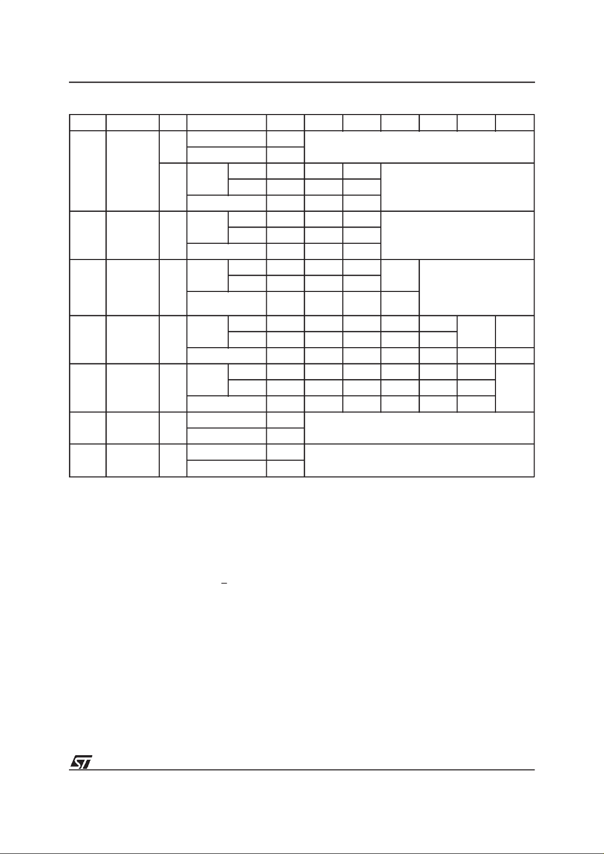
Table 8. Instructions
(1)
Mne. Instr. Cyc. 1st Cyc. 2nd Cyc. 3rd Cyc. 4th Cyc. 5th Cyc. 6th Cyc. 7th Cyc.
RD
(2,4)
Read/Reset
MemoryArray
(3,7)
Addr.
1+
Data F0h
Byte AAAAh 5555h AAAAh
(3,7)
Addr.
3+
Word 5555h 2AAAh 5555h
X
Read Memory Array until a new write cycle is initiated.
ReadMemory Array until a new write cycle
isinitiated.
Data AAh 55h F0h
(4)
AutoSelect 3+
AS
Addr.
(3,7)
Word 5555h 2AAAh 5555h
ReadElectronic Signatureor Block
Protection Status until a new writecycle is
initiated. See Note 5 and6.
Byte AAAAh 5555h AAAAh
Data AAh 55h 90h
PG Program 4
BE BlockErase 6
Byte AAAAh 5555h AAAAh
(3,7)
Addr.
Word 5555h 2AAAh 5555h
Data AAh 55h A0h
Byte AAAAh 5555h AAAAh AAAAh 5555h
(3,7)
Addr.
Word 5555h 2AAAh 5555h 5555h 2AAAh
Program
Address
Program
Data
Read Data Polling or ToggleBit
until Program completes.
Block
Address
Additional
Block
Data AAh 55h 80h AAh 55h 30h 30h
CE Chip Erase 6
Addr.
Word 5555h 2AAAh 5555h 5555h 2AAAh 5555h
Byte AAAAh 5555h AAAAh AAAAh 5555h AAAAh
(3,7)
Data AAh 55h 80h AAh 55h 10h
(3,7)
ES
Notes: 1. Commands not interpreted in this table will default to read array mode.
Suspend
Erase
ER
Resume
2. Await of t
before starting any new operation (see Table14 and Figure 9).
3. X= Don’t Care.
4. The first cycles of the RD or AS instructions are followed by read operations.Any number of readcycles can occur after
the command cycles.
5. SignatureAddress bits A0,A1 at V
Device code.
6. Block Protection Address: A0 at V
7. ForCoded cycles address inputs A15is don’t care.
8. Optional,additional Blocks addresses must be entered within the erasetimeout delay after last writeentry,
timeout status can be verified through DQ3 value (see EraseTimerBit DQ3 description).
When full command is entered, read Data Polling or Togglebit until Erase is completed or suspended.
9. Read Data Polling, Togglebits or RB until Erase completes.
10.During Erase Suspend, Read and Data Programfunctions are allowed in blocks not being erased.
is necessary after a Read/Reset command if the memory was in an Erase or Program mode
PLYH
Erase
(10)
Addr.
1
Data B0h
(3,7)
Addr.
1
Data 30h
will output Manufacturer code (20h). Address bits A0 at VIHandA1 at VILwill output
IL
,A1atVIHand A12-A15 within the Block will output the Block Protection status.
IL
X
Read until Togglestops, then read all the data needed from any
Block(s) not being erased then Resume Erase.
X
Read Data Polling or ToggleBits until Erase completes or Erase is
suspended another time
(8)
Note 9
9/30
Page 10

M29F100T, M29F100B
Table 9. Status Register Bits
DQ Name Logic Level Definition Note
’1’
Data
7
Polling
’0’ Erase On-going
DQ
DQ Program On-going
Erase Complete or erase
block in Erase Suspend
Program Complete or data
of non erase block during
Erase Suspend
Indicates the P/E.C. status, check during
Program or Erase, and on completion
before checking bits DQ5 for Program or
Erase Success.
6 ToggleBit
5 Error Bit
4 Reserved
Erase
3
Time Bit
2 ToggleBit
’-1-0-1-0-1-0-1-’ Erase or Program On-going Successive reads output complementary
DQ Program Complete
’-1-1-1-1-1-1-1-’
’1’ Program or Erase Error
’0’ Program or Erase On-going
’1’ Erase TimeoutPeriod Expired
’0’
’-1-0-1-0-1-0-1-’
1
DQ
Erase Complete or Erase
Suspend on currently
addressed block
Erase TimeoutPeriod
On-going
Chip Erase, Erase or Erase
Suspend on the currently
addressed block.
Erase Error due to the
currently addressed block
(when DQ5 = ’1’).
Program on-going, Erase
on-going on another block or
Erase Complete
Erase Suspend read on
non Erase Suspend block
data on DQ6 while Programming or Erase
operations are on-going. DQ6 remains at
constant level when P/E.C. operations are
completed or Erase Suspend is
acknowledged.
This bitis set to ’1’in the case of
Programming or Erase failure.
P/E.C. Erase operation has started. Only
possible command entry is Erase Suspend
(ES).
An additionalblock to be erased in parallel
can be entered to the P/E.C.
Indicates the erase status and allows to
identify the erased block
1 Reserved
0 Reserved
Notes: Logic level ’1’is High, ’0’ is Low. -0-1-0-0-0-1-1-1-0- represent bit value in successive Read operations.
Toggle Bit (DQ6). WhenProgrammingor Erasing
operationsare in progress,successiveattemptsto
readDQ6willoutputcomplementarydata.DQ6will
toggle followingtoggling of either G, or E when G
is low. The operation is completed when two successivereadsyield thesameoutputdata.Thenext
readwilloutputthe bitlastprogrammedora’1’after
erasing. The toggle bit DQ6 is valid only during
P/E.C. operations,thatis after the fourth W pulse
Erase. If the blocks selected for erasure are protected, DQ6 will toggle for about 100µs and then
returnback toRead. DQ6will besetto ’1’if aRead
operationisattemptedonan EraseSuspendblock.
When erase is suspended DQ6 will toggle during
programming operations in a blockdifferentto the
blockin EraseSuspend.EitherE or G togglingwill
causeDQ6 to toggle. SeeFigure 12 for ToggleBit
flowchartand Figure 13 for ToggleBit waveforms.
for programming or after the sixth W pulse for
10/30
Page 11

M29F100T, M29F100B
Table 10. Polling and Toggle Bits
Mode DQ7 DQ6 DQ2
Program DQ7 Toggle 1
Erase 0 Toggle Note 1
Erase Suspend Read
(in EraseSuspend
block)
Erase Suspend Read
(outside Erase Suspend
block)
Erase Suspend Program DQ7 Toggle N/A
Note: 1. Toggle if the address is within a block being erased.
’1’ if the address is within a block not being erased.
1 1 Toggle
DQ7 DQ6 DQ2
Toggle Bit (DQ2). This toggle bit, together with
DQ6, can be used to determine the device status
duringthe Eraseoperations.It can also beusedto
identify the block being erased. During Erase or
Erase Suspenda read from a block being erased
will cause DQ2 to toggle. A read from a block not
being erased will set DQ2 to ’1’ during erase and
to DQ2 during Erase Suspend.During Chip Erase
a read operation will cause DQ2 to toggle as all
blocks are being erased. DQ2 will be set to ’1’
duringprogram operationand when erase is complete. After erase completion and if the error bit
DQ5 is set to ’1’, DQ2 will toggle if the faulty block
is addressed.
ErrorBit (DQ5). This bit is set to ’1’by the P/E.C.
when there is a failure of programming, block
erase, or chip erase that results in invaliddata in
thememoryblock.In caseofanerrorin blockerase
or program,the blockin whichtheerroroccuredor
to which the programmed data belongs, must be
discarded. The DQ5 failurecondition will also appearif a usertries to programa’1’ toa locationthat
ispreviouslyprogrammedto ’0’.OtherBlocksmay
stillbeused.Theerrorbit resetsafteraRead/Reset
(RD)instruction. In caseof successof Programor
Erase,the errorbit will be set to ’0’.
Erase Timer Bit (DQ3). This bit is set to ’0’ by the
P/E.C. when the last block Erase command has
been entered to the Command Interface and it is
awaiting the Erase start. When the erase timeout
periodis finished,after80µsto 120µs,DQ3returns
to ’1’.
Coded Cycles
Thetwo Coded cyclesunlockthe CommandInterface.Theyare followed by an input commandor a
confirmationcommand.The Coded cycles consist
of writing the data AAh at address AAAAh in the
Byte-wide configuration and at address 5555h in
the Word-wide configuration during the first cycle.
Duringthe second cycle the Coded cycles consist
of writing the data 55h at address 5555h in the
Byte-wideconfiguration and at address 2AAAh in
theWord-wideconfiguration.In theByte-wideconfigurationtheaddresslines A–1 to A14are valid,in
Word-wideA0 to A14 arevalid,otheraddresslines
are’don’t care’. The Coded cycleshappenon first
andsecondcyclesof thecommandwrite or on the
fourthand fifth cycles.
Instructions
SeeTable8.
Read/Reset (RD) Instruction. The Read/Reset
instruction consists of one write cycle giving the
commandF0h. It can beoptionallyprecededbythe
twoCodedcycles.Subsequentreadoperationswill
read the memory array addressed and output the
data read. A wait state of 10µs is necessaryafter
Read/Resetprior to any valid read if the memory
was in an Erase mode when the RD instruction is
given.
Auto Select (AS) Instruction. This instruction
uses the two Coded cycles followed by one write
cycle giving the command 90h to address AAAAh
in the Byte-wide configurationor address5555hin
the Word-wide configuration for command set-up.
A subsequent read will output the manufacturer
code and the device code or the block protection
status dependingon the levels of A0 and A1. The
manufacturer code, 20h, is output when the addresseslinesA0 andA1are Low,thedevice code,
D0h for Top Boot, D1h for Bottom Boot is output
whenA0 isHigh with A1 Low.
TheAS instructionalso allows access to the block
protectionstatus.After givingtheASinstruction,A0
is set to V
with A1 at VIH, while A12-A15 define
IL
the address of the block to be verified. A read in
these conditions will output a 01h if the block is
protectedand a 00h if the block is not protected.
Program (PG) Instruction. This instruction uses
four write cycles. Both for Byte-wide configuration
and for Word-wide configuration. The Program
commandA0h is written to addressAAAAh in the
Byte-wideconfigurationor toaddress 5555h inthe
Word-wideconfigurationonthe thirdcycleaftertwo
Codedcycles. A fourth write operationlatches the
Addresson the fallingedge of W orE and the Data
to be written on the rising edge and starts the
P/E.C.Readoperationsoutput the StatusRegister
bits after the programming has started. Memory
programmingis madeonlyby writing ’0’ in placeof
’1’.StatusbitsDQ6andDQ7determineif programmingison-goingandDQ5 allowsverificationofany
possible error. Programming at an address not in
blocks being erased is also possible during erase
suspend. In this case, DQ2 will toggle at the addressbeing programmed.
11/30
Page 12

M29F100T, M29F100B
Table 11. ACMeasurementConditions
High Speed Standard
Input Rise and Fall Times
Input Pulse Voltages 0 to 3V 0.45V to 2.4V
Input and Output TimingRef. Voltages 1.5V 0.8V and 2V
≤
10ns
≤
10ns
Figure4. AC TestingInput Output Waveform
High Speed
3V
1.5V
0V
Standard
2.4V
0.45V
Table 12. Capacitance
Symbol Parameter TestCondition Min Max Unit
C
IN
C
OUT
Note: 1. Sampled only, not 100% tested.
Input Capacitance VIN=0V 6 pF
Output Capacitance V
(1)
(TA=25°C, f = 1 MHz )
2.0V
0.8V
AI01275B
Figure5. AC TestingLoad Circuit
1.3V
1N914
3.3kΩ
DEVICE
UNDER
TEST
C
L
CL= 30pF for High Speed
CL= 100pF for Standard
CLincludes JIG capacitance
=0V 12 pF
OUT
OUT
AI01276B
Block Erase (BE) Instruction. This instruction
uses a minimum of six write cycles. The Erase
Set-upcommand80h iswritten to addressAAAAh
in the Byte-wideconfigurationor address5555h in
theWord-wideconfigurationon thirdcycleafter the
two Coded cycles. The Block EraseConfirm command30his similarlywrittenonthesixth cycleafter
anothertwo Coded cycles. During the input of the
secondcommandanaddresswithintheblocktobe
erasedis given andlatched intothe memory.Additional block Erase Confirm commands and block
addresses can be written subsequently to erase
other blocks in parallel,without further Coded cycles. The erase will start after the erase timeout
period (see Erase Timer Bit DQ3 description).
12/30
Thus, additional Erase Confirm commands for
other blocks must be given within this delay. The
inputof a newErase Confirm commandwill restart
the timeout period.The status of the internal timer
canbe monitoredthrough the level of DQ3,if DQ3
is ’0’ the Block Erase Command has been given
andthe timeoutis running,ifDQ3is ’1’, the timeout
hasexpired and theP/E.C.is erasingtheBlock(s).
If the second command given is not an erase
confirm or if the Coded cycles are wrong, the
instructionaborts, and the device is reset toRead
Array. It is notnecessary toprogram the blockwith
00h as the P/E.C. will do this automaticallybefore
to erasing to FFh. Read operations after the sixth
rising edge of W or E output the status register
statusbits.
Page 13

M29F100T, M29F100B
Table 13. DC Characteristics
=0 to 70°C, –40 to 85°C or–40 to 125°C; VCC=5V±10%)
(T
A
Symbol Parameter Test Condition Min Max Unit
I
I
LO
I
CC1
I
CC1
I
CC2
I
CC3
I
CC4
V
V
V
V
V
I
V
LKO
Note: 1. Sampled only, not 100% tested.
Input Leakage Current 0V ≤ VIN≤ V
LI
Output Leakage Current 0V ≤ V
Supply Current (Read) TTL Byte E = VIL,G=VIH, f = 6MHz 20 mA
Supply Current (Read) TTL Word E = VIL,G=VIH, f = 6MHz 20 mA
Supply Current (Standby) TTL E = V
Supply Current (Standby) CMOS E = V
(1)
Supply Current (Program or Erase)
Input Low Voltage –0.5 0.8 V
IL
Input High Voltage 2 VCC+ 0.5 V
IH
Output Low Voltage IOL= 5.8mA 0.45 V
OL
Output High Voltage TTL IOH= –2.5mA 2.4 V
OH
Output High VoltageCMOS I
A9 Voltage (Electronic Signature) 11.0 12.0 V
ID
A9 Current (Electronic Signature) A9 = V
ID
Supply Voltage(Erase and
Program lock-out)
CC
≤ V
OUT
CC
IH
0.2V 100
±
CC
Byte program, Block or
Chip Erase in progress
= –100µAV
OH
ID
±1 µA
±1 µA
1mA
20 mA
–0.4V V
CC
100
3.2 4.2 V
A
µ
A
µ
Duringtheexecutionof theeraseby theP/E.C.,the
memoryaccepts only the Erase Suspend ES and
Read/ResetRD instructions. Data Polling bit DQ7
returns’0’ while the erasureis in progress and’1’
when it has completed. The Toggle bit DQ2 and
DQ6 toggle during the erase operation. They stop
when erase is completed. After completion the
StatusRegisterbitDQ5returns’1’iftherehasbeen
an erase failure. In sucha situation,the Togglebit
DQ2 can be used to determine which block is not
correctly erased. In the case of erase failure, a
Read/ResetRDinstructionis necessaryin orderto
resetthe P/E.C.
ChipErase(CE)Instruction.Thisinstructionuses
six writecycles. The Erase Set-up command 80h
is written to address AAAAh in the Byte-wideconfiguration or the address 5555h in the Word-wide
configurationonthe thirdcycleafter thetwoCoded
cycles. The Chip Erase Confirm command 10h is
similarly writtenon thesixth cycleafter anothertwo
Codedcycles. If thesecondcommand given is not
aneraseconfirm or if the Coded cyclesarewrong,
the instruction aborts and the device is reset to
ReadArray.Itisnotnecessarytoprogramthearray
with00h firstas theP/E.C.will automaticallydothis
beforeerasingit to FFh. Readoperationsafter the
sixth rising edge of W or E output the Status
Registerbits. Duringtheexecutionof the erase by
theP/E.C.,Data PollingbitDQ7returns’0’, then ’1’
on completion. The Toggle bits DQ2 and DQ6
toggleduringeraseoperationandstopwhenerase
iscompleted.Aftercompletionthe StatusRegister
bit DQ5 returns ’1’ if there has been an Erase
Failure.
13/30
Page 14

M29F100T, M29F100B
Table 14. Read AC Characteristics
=0 to 70°C, –40 to 85°C or–40 to 125°C)
(T
A
M29F100T / M29F100B
-70 -90 -120
Symbol Alt Parameter TestCondition
Address Validto
(1)
(2)
(1)
(2)
(1)
(1)
(1,3)
t
RC
t
ACC
t
LZ
t
CE
t
OLZ
t
OE
t
OH
t
HZ
t
OH
t
DF
t
OH
t
RRB
t
READY
t
RH
t
RP
t
ELFL
t
ELFH
t
AVAV
t
AVQV
t
ELQX
t
ELQV
t
GLQX
t
GLQV
t
EHQX
t
EHQZ
t
GHQX
t
GHQZ
t
AXQX
t
PLYH
t
PHEL
t
PLPX
t
ELBL
t
ELBH
Next Address Valid
Address Validto
Output Valid
Chip Enable Low to
Output Transition
Chip Enable Low to
Output Valid
Output Enable Low
to Output Transition
Output Enable Low
to Output Valid
Chip Enable High to
Output Transition
Chip Enable High to
Output Hi-Z
Output Enable High
to Output Transition
Output Enable High
to Output Hi-Z
Address Transition to
Output Transition
RP Low to Read
Mode
RP High to Chip
Enable Low
RP Pulse Width 500 500 500 ns
Chip Enable to BYTE
Switching Low or
High
E=V
E=V
G=V
G=V
G=V
G=V
E=V
,G=V
IL
,G=V
IL
E=V
E=V
E=V
E=V
,G=V
IL
IL
IL
IL
IL
IL
IL
IL
IL
IL
IL
IL
BYTE Switching Low
t
BLQZtFLQZ
to Output
High Z
BYTE Switching
t
BHQVtFHQV
High to Output
Valid
Notes: 1. Sampled only,not 100% tested.
2. G maybe delayed by up to t
3. To be considered only if the Reset pulse is given while the memory is in Erase or Program mode.
ELQV-tGLQV
afterthe falling edge of E without increasing t
=5V±5% VCC=5V±10% VCC=5V±10%
V
CC
High Speed
Interface
Min Max Min Max Min Max
70 90 120 ns
70 90 120 ns
000ns
70 90 120 ns
000ns
30 35 50 ns
000ns
20 20 30 ns
000ns
20 20 30 ns
000ns
10 10 10
50 50 50 ns
555ns
30 40 40 ns
30 40 40 ns
Standard
Interface
.
ELQV
Standard
Interface
Unit
s
µ
14/30
Page 15

Figure 6. ReadMode AC Waveforms
tEHQZ
tGHQZ
tGHQX
M29F100T, M29F100B
AI01979B
VALID
tAVAV
VALID
tAVQV tAXQX
tELQV
tELQX tEHQX
tGLQV
tGLQX
tBLQZtELBL/tELBH
OUTPUT ENABLE DATA VALID
ADDRESS VALID
AND CHIP ENABLE
A0-A15/
A–1
E
G
DQ0-DQ7/
DQ8-DQ15
BYTE
WriteEnable (W) = High
Note:
15/30
Page 16

M29F100T, M29F100B
Table 15. Write AC Characteristics,WriteEnable Controlled
=0 to 70°C, –40 to 85°C or–40 to 125°C)
(T
A
-70 -90 -120
Symbol Alt Parameter
=5V±5% VCC=5V±10% VCC=5V±10%
V
CC
High Speed
Interface
Min Max Min Max Min Max
M29F100T / M29F100B
Standard
Interface
Unit
Standard
Interface
t
AVAV
t
ELWL
t
WLWH
t
DVWH
t
WHDX
t
WHEH
t
WHWL
t
AVWL
t
WLAX
t
GHWL
t
VCHEL
t
WHGL
t
PHPHH
t
PLPX
t
WHRL
t
PHWL
Notes: 1. Sample only, not 100% tested.
2. This timing is for TemporaryBlock Unprotection operation.
(1,2)
(1)
(1)
t
Address Validto Next Address Valid 70 90 120 ns
WC
Chip Enable Low to WriteEnable
t
CS
Low
Write Enable Low to Write Enable
t
WP
High
t
Input Valid to Write Enable High 30 45 50 ns
DS
Write Enable High to Input
t
DH
Transition
Write Enable High to Chip Enable
t
CH
High
Write Enable High to Write Enable
t
WPH
Low
t
Address Validto Write Enable Low 0 0 0 ns
AS
Write Enable Low to Address
t
AH
Transition
Output Enable High to Write
Enable Low
t
VCSVCC
t
OEH
t
VIDR
t
RP
t
BUSY
t
RSP
High to Chip Enable Low 50 50 50
Write Enable High to Output
Enable Low
RP Rise Timeto V
ID
RP Pulse Width 500 500 500 ns
Program Erase Validto RB Delay 30 35 50 ns
RP High to Write Enable Low 4 4 4 µs
000ns
35 45 50 ns
000ns
000ns
20 20 20 ns
45 45 50 ns
000ns
s
µ
000ns
500 500 500 ns
Erase Suspend (ES) Instruction. Th e Block
Eraseoperationmay besuspendedbythisinstruction which consists of writing the command B0h
withoutany specificaddress. No Coded cyclesare
required. It permits reading of data from another
block and programming in another block while an
erase operation is in progress. Erase suspend is
accepted only during the Block Erase instruction
execution. Writing this command during Erase
16/30
timeout will, in addition to suspending the erase,
terminate the timeout. The Toggle bit DQ6 stops
togglingwhentheP/E.C.is suspended.TheToggle
bitswill stoptogglingbetween0.1µsand 15µsafter
the Erase Suspend (ES) command has been written. The device will then automatically be set to
Read Memory Array mode. When erase is suspended, a Read from blocks being erased will
output DQ2 togglingand DQ6 at ’1’. A Read from
Page 17

Figure7. WriteAC Waveforms,W Controlled
A0-A15/
A–1
tAVWL
E
M29F100T, M29F100B
tAVAV
VALID
tWLAX
tWHEH
tELWL
G
tWLWHtGHWL
W
tDVWH
DQ0-DQ7/
DQ8-DQ15
V
CC
tVCHEL
RB
Note: Address are latched onthe falling edge of W, Datais latched on the rising edge ofW.
a blocknot beingerased returnsvalid data.During
suspension the memory will respond only to the
Erase Resume ER and the Program PG instructions. A Program operation can be initiatedduring
erase suspend in one of the blocks not being
erased. It will result in bothDQ2andDQ6toggling
whenthedatais beingprogrammed.ARead/Reset
commandwill definitively abort erasure and result
in invalid data in the blocks being erased.
EraseResume(ER)Instruction. Ifan EraseSuspend instruction was previously executed, the
erase operation may be resumed by giving the
command 30h, at any address, and without any
Codedcycles.
VALID
tWHRL
POWERSUPPLY
PowerUp
ThememoryCommandInterfaceis reset onpower
uptoRead Array.EitherE or Wmust be tiedto V
during Power Up to allow maximum security and
thepossibilityto writea commandonthefirst rising
edge of E and W. Any write cycle initiation is
blockedwhen Vcc is below V
SupplyRails
Normalprecautionsmust be taken for supplyvoltage decoupling; each device in a system should
havethe V
CC
close to the V
widths should be sufficient to carry the V
gramand erasecurrents required.
tWHGL
tWHWL
tWHDX
AI01980B
.
LKO
raildecoupledwith a 0.1µF capacitor
and VSSpins. The PCB trace
CC
CC
pro-
IH
17/30
Page 18

M29F100T, M29F100B
Table 16. Write AC Characteristics,Chip Enable Controlled
=0 to 70°C, –40 to 85°C or–40 to 125°C)
(T
A
-70 -90 -120
Symbol Alt Parameter
Address Valid to Next Address
t
AVAV
t
WLEL
t
ELEH
t
DVEH
t
EHDX
t
WC
Valid
Write Enable Low to Chip
t
WS
Enable Low
Chip Enable Low to ChipEnable
t
CP
High
t
Input Validto Chip Enable High 30 45 50 ns
DS
Chip Enable High to Input
t
DH
Transition
=5V±5% VCC=5V±10% VCC=5V±10%
V
CC
High Speed
Interface
Min Max Min Max Min Max
70 90 120 ns
000ns
35 45 50 ns
000ns
M29F100T / M29F100B
Standard
Interface
Unit
Standard
Interface
Chip Enable High to Write
t
EHWH
t
EHEL
t
AVEL
t
ELAX
t
GHEL
t
VCHWL
t
EHGL
(1,2)
t
PHPHH
t
PLPX
(1)
t
EHRL
(1)
t
PHWL
Notes: 1. Sample only, not 100% tested.
2. This timing is for TemporaryBlock Unprotection operation.
t
WH
t
CPH
t
t
t
VCS
t
OEH
t
VIDR
t
t
BUSY
t
RSP
Enable High
Chip Enable High to Chip
Enable Low
Address Valid to Chip Enable
AS
Low
Chip Enable Low to Address
AH
Transition
Output Enable High Chip
Enable Low
VCCHigh to Write Enable Low 50 50 50 µs
Chip Enable High to Output
Enable Low
RP Rise TIme to V
RP Pulse Width 500 500 500 ns
RP
ID
Program Erase Validto RB
Delay
RP High to Write Enable Low 4 4 4
000ns
20 20 20 ns
000ns
45 45 50 ns
000ns
000ns
500 500 500 ns
30 35 50 ns
s
µ
18/30
Page 19

Figure8. WriteAC Waveforms,E Controlled
A0-A15/
A–1
tAVEL
W
M29F100T, M29F100B
tAVAV
VALID
tELAX
tEHWH
tWLEL
G
tELEHtGHEL
E
tDVEH
DQ0-DQ7/
DQ8-DQ15
V
CC
tVCHWL
RB
Note: Address are latched onthe falling edge of E, Data is latchedon the rising edge of E.
VALID
tEHRL
Figure9. Readand WriteAC Characteristics,RP Related
tEHGL
tEHEL
tEHDX
AI01981B
E
W
RB
RP
tPHEL
tPHWL
tPLPX
tPHPHH
tPLYH
AI02091
19/30
Page 20

M29F100T, M29F100B
Table 17. Data Polling and Toggle Bit AC Characteristics
(TA=0 to 70°C, –40 to 85°C or–40 to 125°C)
-70 -90 -120
Symbol Parameter
Write Enable High to DQ7 Valid
t
WHQ7V
(Program, W Controlled)
Write Enable High to DQ7 Valid
(Chip Erase, W Controlled)
Chip Enable High toDQ7 Valid
t
EHQ7V
(Program, E Controlled)
Chip Enable High toDQ7 Valid
(Chip Erase, E Controlled)
t
Q7VQV
Q7 Validto Output Valid(Data
Polling)
Write Enable High to Output Valid
t
WHQV
(Program)
Write Enable High to Output Valid
(Chip Erase)
Chip Enable High toOutput Valid
t
EHQV
(Program)
Chip Enable High toOutput Valid
(Chip Erase)
Note: 1. All other timings are defined in Read ACCharacteristics table.
=5V±5% VCC=5V±10% VCC=5V±10%
V
CC
High Speed
Interface
Min Max Min Max Min Max
10 2400 10 2400 10 2400
1.0 30 1.0 30 1.0 30 sec
10 2400 10 2400 10 2400 µs
1.0 30 1.0 30 1.0 30 sec
30 35 50 ns
10 2400 10 2400 10 2400
1.0 30 1.0 30 1.0 30 sec
10 2400 10 2400 10 2400 µs
1.0 30 1.0 30 1.0 30 sec
(1)
M29F100T / M29F100B
Standard
Interface
Standard
Interface
Unit
µ
µ
s
s
20/30
Page 21

Figure10. DataPolling DQ7 AC Waveforms
M29F100T, M29F100B
AI01982B
ARRAY
READ CYCLE
DATA OUTPUT VALID
ADDRESS (WITHIN BLOCKS)
tAVQV
tELQV
tEHQ7V
tGLQV
VALID
DQ7
tWHQ7V
VALID
tQ7VQV
IGNORE
DATA POLLING (LAST) CYCLE MEMORY
READ CYCLES
DATA POLLING
A0-A15/
A–1
PROGRAM
OR ERASE
CYCLE OF
LAST WRITE
E
G
W
DQ7
DQ0-DQ6/
DQ8-DQ15
INSTRUCTION
21/30
Page 22

M29F100T, M29F100B
Figure 11. DataPolling Flowchart
START
READ DQ5 &
at VALID ADDRESS
NO
READ DQ7
DQ7
DQ7
DATA
DQ5
DQ7
DATA
FAIL PASS
=
=1
=
YES
YES
NO
YES
NO
Figure 12. Data Toggle Flowchart
START
READ
DQ2, DQ5 & DQ6
DQ6
YES
YES
DQ6
YES
NO
NO
DQ2,
=
TOGGLE
NO
DQ5
=1
READ DQ2, DQ6
DQ2,
=
TOGGLE
FAIL PASS
AI01369
AI01873
Table 18. Program, Erase Times and Program, Erase Endurance Cycles
= 0 to 70°C; VCC=5V±10% or 5V ± 5%)
(T
A
M29F100T / M29F100B
Parameter
Min Typ
Typical after
100k W/E Cycles
Chip Erase (Preprogrammed) 0.4 0.6 sec
Chip Erase 1.5 1.7 sec
Boot Block Erase 0.6 sec
Parameter Block Erase 0.5 sec
Main Block (32Kb) Erase 0.9 sec
Main Block (64Kb) Erase 1.0 sec
Chip Program (Byte) 1.4 1.4 sec
Byte Program 11 11
Word Program 20 20
Program/Erase Cycles (per Block) 100,000 cycles
Unit
s
µ
s
µ
22/30
Page 23

Figure13. DataToggle DQ6, DQ2AC Waveforms
M29F100T, M29F100B
AI01983B
VALID
tEHQV
tAVQV
tELQV
tGLQV
VALID
tWHQV
STOP TOGGLE
VALID
IGNORE
READ CYCLE
MEMORY ARRAY
READ CYCLE
DATA TOGGLE
A0-A15/
A–1
DATA
TOGGLE
READ CYCLE
OF ERASE
PROGRAM
CYCLE OF
LAST WRITE
DQ0-DQ1,DQ3-DQ5,DQ7/
E
G
W
DQ6,DQ2
DQ8-DQ15
INSTRUCTION
All other timings are as a norm al Read cycle.
Note:
23/30
Page 24

M29F100T, M29F100B
Figure 14. Block Protection Flowchart
Set-up
Protect
Verify
VERIFY BLOCK
A0, A6 = VIL;A1=VIH;A9=VID
A12-A15 IDENTIFY BLOCK
START
BLOCK
on A12-A15
W=V
n=0
G, A9 = VID,
E=V
Wait 4µs
W=V
Wait 100µs
W=V
E, G = V
ADDRESS
IH
IL
IL
IH
IH
PROTECTION
E=V
IL
Wait 4µs
G=V
IL
Wait 60ns
VERIFY
DATA
=
01h
A9 = V
PASS
BLOCK
NO
YES
IH
PROTECT STATUS
++n
=25
A9 = V
FAIL
NO
YES
IH
AI01984C
24/30
Page 25

Figure15. AllBlocks UnprotectingFlowchart
M29F100T, M29F100B
E, A0 = VIL; A1, A6 = VIH;A9=V
A12-A15 IDENTIFY BLOCK
START
PROTECT
ALL BLOCKS
n=0
W=V
IH
E, G, A9 = V
A12, A15 = V
Wait 4µs
W=V
IL
Wait 10ms
W=V
IH
E, G = V
Set-up
ID
IH
Unprotect
IH
ID
Verify
NEXT
BLOCK
Wait 4µs
G=V
IL
Wait 60ns
BLOCK
VERIFY
PROTECT STATUS
00h
YESNO
=
DATA
++n
NO
= 1000
YES
A9 = V
IH
FAIL PASS
LAST
BLK.
A9 = V
NO
YES
IH
AI01985D
25/30
Page 26

M29F100T, M29F100B
ORDERING INFORMATION SCHEME
Example: M29F100T -70 X N 1 TR
Operating Voltage
F5V
Array Matrix
T TopBoot
B Bottom Boot
Speed
-70 70ns
-90 90ns
-120 120ns
Power Supplies
blank V
XV
CC
CC
±
±
10%
5%
Package
N TSOP48
12 x 20mm
M SO44
Option
R Reverse
Pinout
TR Tape & Reel
Packing
Temp. Range
1 0 to 70°C
6 –40 to 85°C
3 –40 to 125°C
Devicesare shipped from the factory with the memory contenterased (to FFh).
Fora list ofavailableoptions(Speed,Package,etc...)or for furtherinformationon anyaspect of thisdevice,
pleasecontactthe STMicroelectronics Sales Officenearest to you.
26/30
Page 27

M29F100T, M29F100B
TSOP48 Normal Pinout - 48 lead Plastic Thin Small Outline, 12 x 20mm
Symb
Typ Min Max Typ Min Max
A 1.20 0.047
A1 0.05 0.15 0.002 0.006
A2 0.95 1.05 0.037 0.041
B 0.17 0.27 0.007 0.011
C 0.10 0.21 0.004 0.008
D 19.80 20.20 0.780 0.795
D1 18.30 18.50 0.720 0.728
E 11.90 12.10 0.469 0.476
e 0.50 - - 0.020 - L 0.50 0.70 0.020 0.028
α
N48 48
CP 0.10 0.004
mm inches
0
°
5
°
0
°
5
°
Drawing is not to scale.
1N
E
N/2
D1
D
DIE
TSOP-a
A2
e
B
A
CP
C
LA1 α
27/30
Page 28

M29F100T, M29F100B
TSOP48Reverse Pinout - 48 lead Plastic Thin Small Outline, 12 x 20mm
Symb
Typ Min Max Typ Min Max
A 1.20 0.047
A1 0.05 0.15 0.002 0.006
A2 0.95 1.05 0.037 0.041
B 0.17 0.27 0.007 0.011
C 0.10 0.21 0.004 0.008
D 19.80 20.20 0.780 0.795
D1 18.30 18.50 0.720 0.728
E 11.90 12.10 0.469 0.476
e 0.50 – – 0.020 – –
L 0.50 0.70 0.020 0.028
α
N48 48
CP 0.10 0.004
mm inches
0
°
5
°
0
°
5
°
Drawing is not to scale.
1N
E
N/2
D1
D
DIE
TSOP-b
A2
e
B
A
CP
C
LA1 α
28/30
Page 29

M29F100T, M29F100B
SO44 - 44 lead Plastic Small Outline, 525 mils body width
Symb
Typ Min Max Typ Min Max
A 2.42 2.62 0.095 0.103
A1 0.22 0.23 0.009 0.010
A2 2.25 2.35 0.089 0.093
B 0.50 0.020
C 0.10 0.25 0.004 0.010
D 28.10 28.30 1.106 1.114
E 13.20 13.40 0.520 0.528
e 1.27 0.050
H 15.90 16.10 0.626 0.634
L 0.80 0.031
α
N44 44
CP 0.10 0.004
3
°
mm inches
3
°
Drawing is not to scale.
A2
A
C
B
e
CP
D
N
E
H
1
LA1 α
SO-b
29/30
Page 30

M29F100T, M29F100B
Information furnished is believed to be accurate and reliable. However, STMicroelectronics assumes no responsibility for the consequences
ofuse ofsuch information nor for any infringement of patents or otherrightsof third parties whichmay result from its use. No license is granted
by implicationor otherwise under any patent or patent rights of STMicroelectronics. Specificationsmentioned in this publication are subject to
change without notice. This publication supersedes and replaces all information previously supplied. STMicroelectronics products are not
authorized for use as critical componentsin life support devices or systems without express writtenapproval of STMicroelectronics.
The ST logois a registeredtrademark of STMicroelectronics
1998 STMicroelectronics - All Rights Reserved
Australia - Brazil - Canada- China- France- Germany - Italy - Japan - Korea - Malaysia - Malta - Mexico - Morocco - The Netherlands -
Singapore - Spain - Sweden- Switzerland - Taiwan - Thailand - United Kingdom - U.S.A.
STMicroelectronics GROUP OF COMPANIES
30/30
 Loading...