

Page 1
查询M29F002BB120K1供应商
2 Mbit (256Kb x8, Boot Block) Single Supply Flash Memory
■ SINGLE 5V ± 10% SUPPLY VOLTAGE for
PROGRAM, ERAS E and READ O PER AT IONS
■ ACCESS TIME: 45 ns
■ PROGRAMMING TIME
– 8 µs by Byte typical
■ 7 MEMORY BLOCKS
– 1 Boot Block (Top or Bottom Location)
– 2 Parameter and 4 Main Blocks
■ PROGRAM/ERA SE CON T ROL LER
– Embedded Byte Program algorithm
– Embedded Multi-Block/Chip Erase algorithm
– Status Register Polling and Toggle Bits
■ ERASE SUSPEND and RESUME MODES
– Read and Program another Block during
Erase Suspend
■ UNLOCK BYPASS PROGRAM COMMAND
– Faster Production/Batch Programming
■ TEMPORARY BLOCK UNPROTECTION
MODE
■ LOW POWER CONSUMPTION
– Standby and Automatic Standby
■ 100,000 PROGRAM/ER ASE CYCL ES per
BLOCK
■ 20 YEARS DATA RETENTION
– Defectivity below 1 ppm/year
■ ELECTRONIC SIGNATURE
– Manufacturer Code: 20h
– Top Device Code M29F002BT: B0h
– Top Device Code M29F002BNT: B0h
– Bottom Device Code M29F002BB: 34h
– Bottom Device Code M29F002BNB: 34h
M29F002BT, M29F002BNT
M29F002BB, M29F002BNB
PLCC32 (K)
32
1
PDIP32 (P)
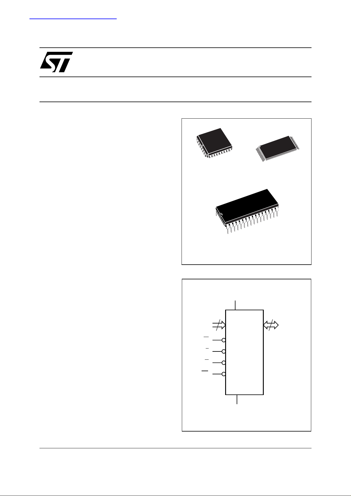
Figure 1. Logic Diagram
V
CC
18
A0-A17
W
E
G
RP
M29F002BT
M29F002BB
M29F002BNT
M29F002BNB
TSOP32 (N)
8 x 20mm
8
DQ0-DQ7
V
SS
AI02957B
1/22April 2002
Page 2
M29F002BT, M29F002BB, M29F002BNT, M29F002BNB
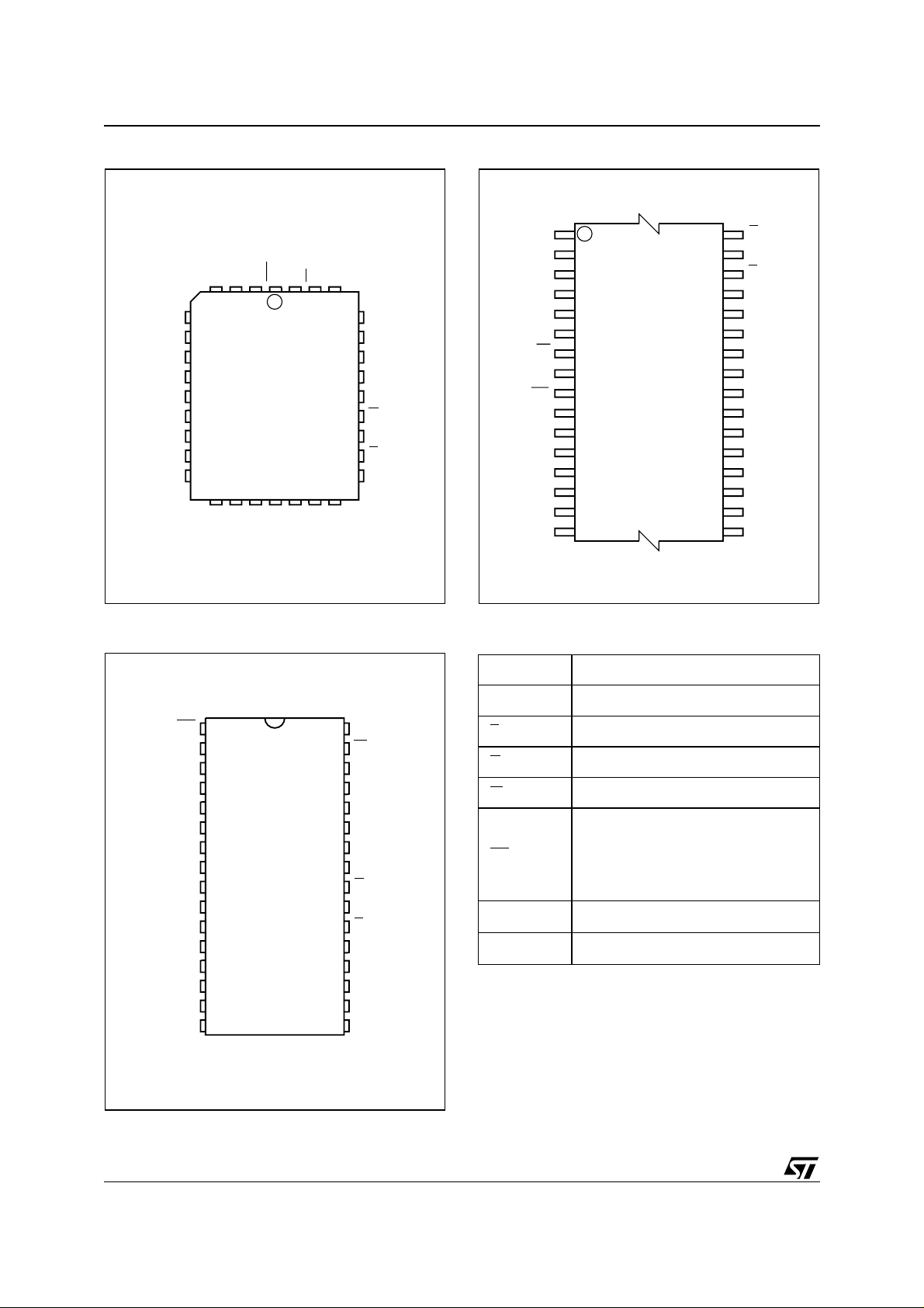
Figure 2. PLCC Connections
A16
A7
A6
A5
A4
A3
A2
A1
A0
DQ0
A12
9
M29F002BNB
DQ1
RP
A15
V
32
1
M29F002BT
M29F002BB
17
SS
V
DQ2
DQ3
DQ4
CC
W
DQ5
A17
25
DQ6
A14
A13
A8
A9
A11
G
A10
E
DQ7
AI02959B
Figure 3. TSOP Connections
A11 G
A9
A8
A13
A14
A17
V
CC
RP
A16
A15
A12
A7
A6
A5
A4 A3
1
W
8
M29F002BT
M29F002BB
9
16 17
32
25
24
AI02958
A10
E
DQ7
DQ6
DQ5
DQ4
DQ3
V
SS
DQ2
DQ1
DQ0
A0
A1
A2
Figure 4. PDIP Connections
1
RP V
2
3
A15
4
A12
5
A7
6
A6
M29F002BT
7
A5
M29F002BB
8
A4
A3
A2
A1
A0
DQ0
DQ2
SS
M29F002BNT
9
10
11
12
13
14
15
16
32
31
30
29
28
27
26
25
24
23
22
21
20
19
18
17
AI02960
CC
WA16
A17
A14
A13
A8
A9
A11
G
A10
E
DQ7
DQ6
DQ5DQ1
DQ4
DQ3V
Table 1. Signal Names
A0-A17 Address Inputs
DQ0-DQ7 Data Inputs/Outputs
E
G
W
RP
V
V
CC
SS
Chip Enable
Output Enable
Write Enable
M29F002BT, M29F002BB:
Reset/Block Temporary Unprotect
M29F002BNT, M29F002BNB:
Not Connected Internally
Supply Voltage
Ground
2/22
Page 3
M29F002BT, M29F002BB, M29F 002BNT, M29F002BNB
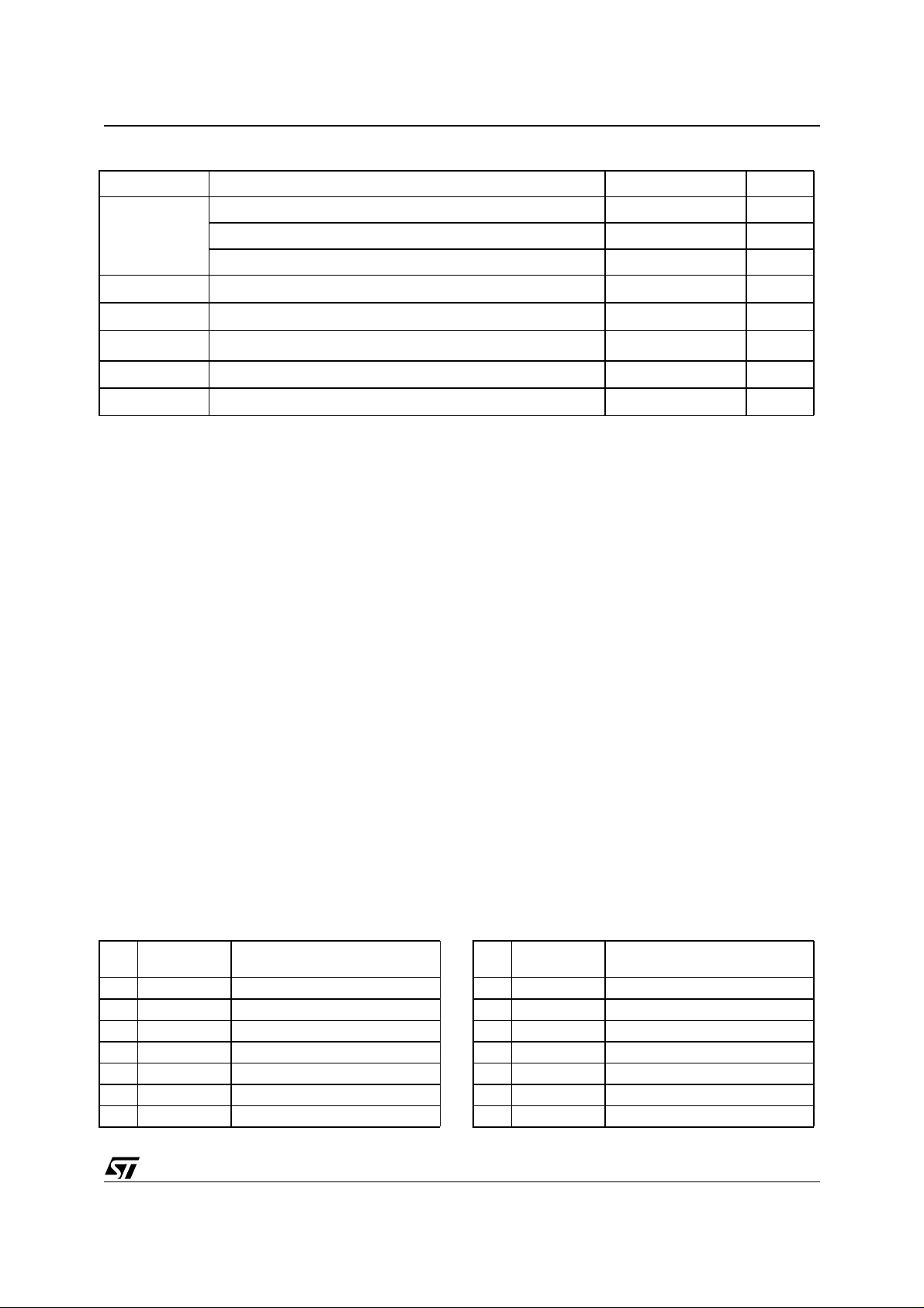
Table 2. Absolute Maximum Ratings
Symbol Parameter Value Unit
Ambient Operating Temperature (Temperature Range Option 1) 0 to 70 °C
T
A
T
BIAS
T
STG
(2)
V
IO
V
CC
V
ID
Note: 1. Except for the rating "Operating T em perature Range", stres ses above t hose listed in the Table "Abs ol ute Maximum Ratings" may
cause permanent damage to the device. These are stress ratings only and operation of the device at these or any other conditions
above those indica ted in the Operating sections of this specification i s not impli ed. Exposure to Abs ol ute Maximum Rating conditions for extended periods may affect device reliability. Refer also to the STMicroelectronics SURE Program and other relevant quality docume nts.
2. Mini m um Voltage may undershoot to –2 V during transition and for less than 20ns during transitions.
Ambient Operating Temperature (Temperature Range Option 6) –40 to 85 °C
Ambient Operating Temperature (Temperature Range Option 3) –40 to 125 °C
Temperature Under Bias –50 to 125 °C
Storage Temperature –65 to 150 °C
Input or Output Voltage –0.6 to 6 V
Supply Voltage –0.6 to 6 V
Identification Voltage –0.6 to 13.5 V
SUMMARY DESCRIPTION
The M29F002B is a 2 Mbit (256Kb x8) non-volatile
memory that can be read, erased and reprogrammed. These operations can be performed using a single 5V supply. On power-up the memory
defaults to its Read mode where it can be read in
the same way as a ROM or EPROM. The
M29F002B is fully backward com patible with the
M29F002.
The memory is divided into blocks that can be
erased independently so it is pos sible to pres erve
val i d da t a whi l e o l d da t a is erased . Ea c h b l oc k ca n
be protected independently to prev ent accidental
Program or Erase commands from modifying the
memory. Program and Erase com m ands are written to the Command Interface of t he memory . An
on-chip Program/Erase Controller simplifies the
process of programming or erasing the memory by
taking care of all of the special operations that are
required to update the memory contents. The end
(1)
of a program or erase operation can be detected
and any error conditions identified. The command
set required to control the memory is consistent
with JEDEC standards.
The blocks in the memory are asymmetrically arranged, see Tables 3A and 3B, Block Addresses .
The first or last 64 Kbyte s have bee n divided into
four additional blocks. The 16 Kbyte Boot Block
can be used for small initialization code to start the
microprocessor, the two 8 Kbyte Parameter
Blocks can b e us ed for parameter storage and the
remaining 32K is a small Main Block where the application may be stored.
Chip Enable, Output Enable and Write Enable signals control the bus operation of the memory.
They allow simple conn ection to most microprocessors, often without additional logic.
The memory is offered in TSOP32 (8 x 20mm),
PLCC32 and PDIP packages and it is supplied
with all the bits erased (set to ’1’).
Table 3. Top Boot Block Addresses,
M29F002BT, M29F002BNT
#
6 16 3C000h-3FFFFh
5 8 3A000h-3BFFFh
4 8 38000h-39FFFh
3 32 30000h-37FFFh
2 64 20000h-2FFFFh
1 64 10000h-1FFFFh
0 64 00000h-0FFFFh
Size
(Kbytes)
Address Range
Table 4. Bottom Boot Block Addresses,
M29F002BB
#
6 64 30000h-3FFFFh
5 64 20000h-2FFFFh
4 64 10000h-1FFFFh
3 32 08000h-0FFFFh
2 8 06000h-07FFFh
1 8 04000h-05FFFh
0 16 00000h-03FFFh
Size
(Kbytes)
Address Range
3/22
Page 4

M29F002BT, M29F002BB, M29F002BNT, M29F002BNB
SIGNAL DESCRIPTIONS
See Figure 1, Logic Diagram, and Table 1, Sign al
Names, for a brief overview of the signals connected to this device.
Address Inputs (A0-A17). The Address Inputs
select the cells i n the memory array to a ccess during Bus Read operations. During Bus Write operations they control the commands sent to the
Command Interface of the internal state machine.
Data Inputs/Outputs (DQ0-DQ7). The Data Inputs/Outputs output the data stored at the selected
address during a Bus Read operation. During Bus
Write operations they represent the commands
sent to the Command Interface of the internal state
machine.
Chip Enable (E
). The Chip Enable, E, activates
the memory, allowing Bus Read and Bus Write operations to be performed. When Chip Enable is
High, V
Output Enable (G
, all other pins are ignored.
IH
). The Output Enable, G, con-
trols the Bus Read operation of the memory.
Write Enable (W
). The Write Enable, W, controls
the Bus Write operation of the memory’s Command Interf a c e .
Reset/Block Temporary Unprotect (RP
). The Re-
set/Block Temporary Unprotect pin can be used to
apply a Hardware Reset to the memory or to temporarily unprotect all blocks that have been protected. On the M29F002BNT the pin is not
connected internally and this feature is not available.
A Hardware Reset is achieved by holding Reset/
Block Temporary Unprotect Low, V
t
. After Reset/Block Temporary Unprotect
PLPX
goes High, V
, the memory will be ready for Bus
IH
Read and Bus Write operations after t
or t
, whichever occurs last. See Table 15 and
PLYH
, for at least
IL
PHEL
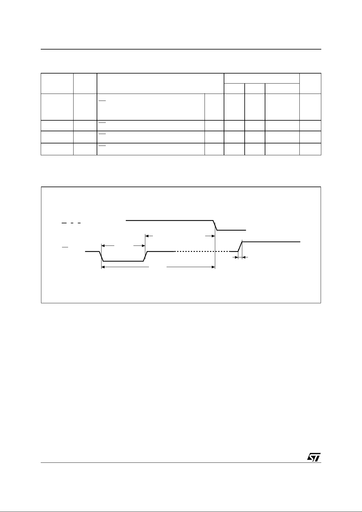
Figure 12, Reset/Temporary Unprotect AC Characteristics for more details.
Holding RP
at VID will temporarily unprotect the
protected blocks in the memory. Program and
Erase operations on all blocks will be possible.
The transition from V
t
PHPHH
.
to VID must be slower than
IH
Reset/Block Temporary Unprotect can be left unconnected. A weak internal pull-up resistor ensures that the memory always operates correctly.
V
Supply Voltage. The VCC Supply Voltage
CC
supplies the power for all operations (Read, Program, Erase etc.).
The Command Interface is disabled when the V
CC
Supply Voltage is less than the L ockout Voltage,
. This prevents Bus Write operations from ac-
V
LKO
cidentally damaging the data during power up,
power down and power surges. If the Program/
Erase Controller is programming or erasing during
this time then the operation aborts and the memory contents being altered will be invalid.
A 0.1µF capacitor should be connected between
the V
Supply Voltage pin and the VSS Ground
CC
pin to decouple the current surges from the power
supply. The PCB track widths must be sufficient to
carry the currents required during program and
erase operations, I
V
Ground. The VSS Ground is the reference for
SS
CC4
.
all voltage measurements.
4/22
Page 5
M29F002BT, M29F002BB, M29F 002BNT, M29F002BNB
BUS OPERATIONS
There are five standard bus operations that control
the device. These are Bus Read, Bus Wri te, Output Disable, Standby and Automatic Standby. See
Table 5, Bus Operations, for a summary. Typically
glitches of less than 5ns on Chip Enabl e o r Write
Enable are ignored by t he mem ory and do not affect bus operations.
Bus Read. Bus Read operations read from the
memory cells, or specific registers in the Command Interface. A valid Bus Read operation involves setting the desired address on the Address
Inputs, applying a Low sig nal, V
, to Chip Enable
IL
and Output Enable and keeping Write Enable
High, V
. The Data Inputs/Outputs will output the
IH
value, see Figure 9, Rea d Mode AC Wav eforms,
and Table 12, Read AC Characteristics, for details
of when the output becomes valid.
Bus Write. Bus Write operations write to the
Command Interface. A valid Bus Write operation
begins by setting the desire d address on t he Address Inputs. The Address Inputs are latched by
the Command Interface on the falling edge of Chip
Enable or Write Enable, whichever occurs last.
The Data Inputs/Outputs a re latched by the Command Interface on the rising edge of Chip Enable
or Write Enable, whichever occurs first. Output Enable must remain High, V
, during the whole Bus
IH
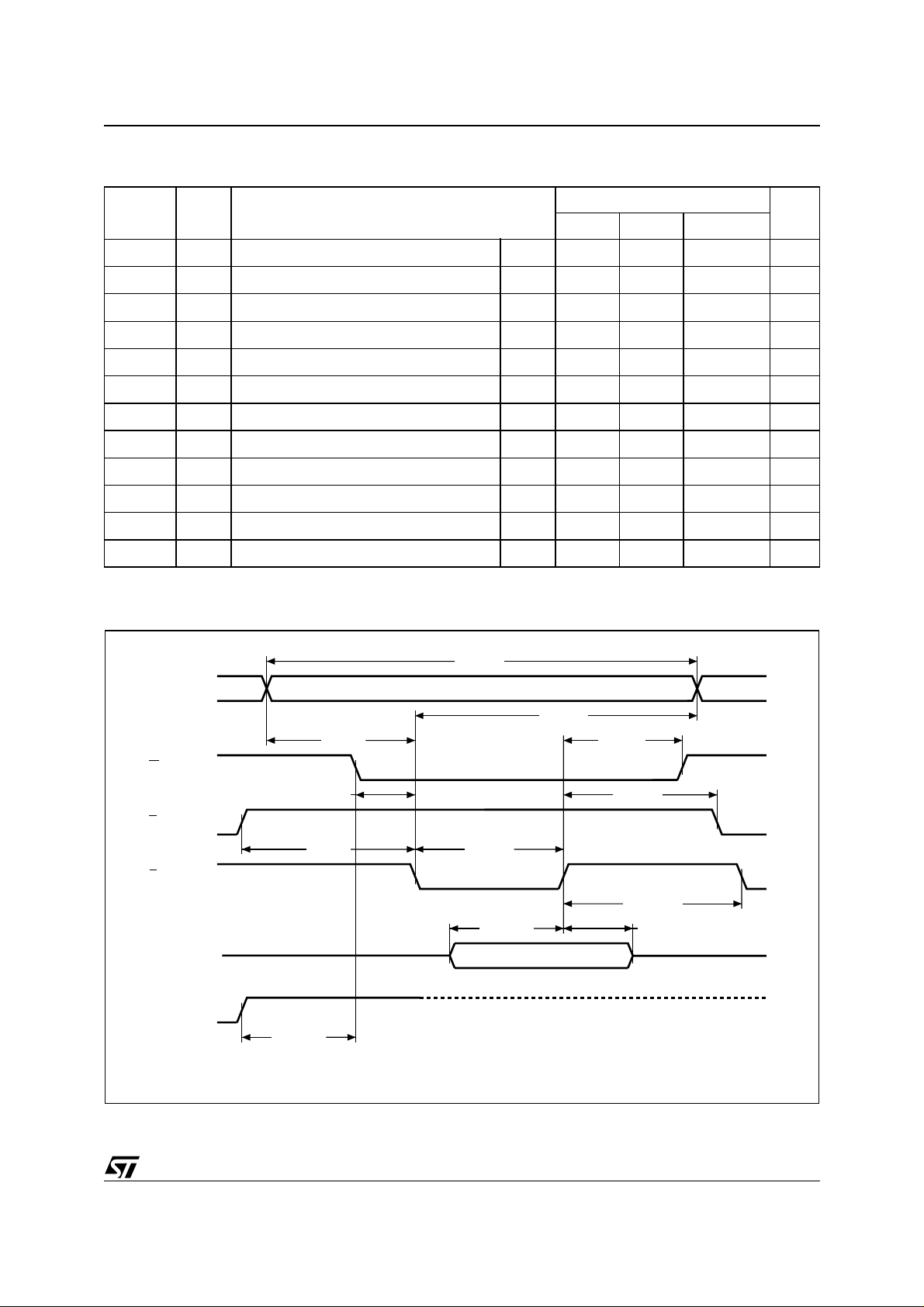
Write operation. See Figures 10 and 11, Write AC
Waveforms, and Tables 13 and 14, Write AC
Characteristics, for details of the timing requirements.
Output Disa bl e . The Data Inputs/Outputs are in
the high impedance s tate when Output Enable is
High, V
Standby. When Chip Enable is High, V
.
IH
, the
IH
Data Inputs/Outputs pins are placed in the highimpedance state and the Supply Current is reduced to the Standby level.
When Chip Enable is at V
reduced to the TTL Standby Supply Current, I
the Supply Current is
IH
CC2
To further reduce the Supply Current to the CMOS
Standby Supply Current, I
be held within V
± 0.2V. For Standby current
CC
, Chip Enable should
CC3
levels see Table 11, DC Characteristics.
During program or erase operations the memory
will continue to use the Program/Erase Supply
Current, I
, for Program or Erase operations un-
CC4
til the operation completes.
Automatic Standby. If CMOS levels (V
± 0.2V)
CC
are used to drive the bus and the bus is inactive for
150ns or more the memory enters Automatic
Standby where the internal Supply Current is reduced to the CMOS Standby Supply Current, I
CC3
The Data In puts/Outputs will s till output data if a
Bus Read operation is in progress.
Special Bus Operations
Additional bus operations can be performed to
read the Electronic Signature and also to apply
and remove Block Protec tion. These bus operations are intended for use by programming equipment and are not usually used in applications.
They require V
to be applied to some pins.
ID
Electronic Signature. The memory has two
codes, the manufacturer code and the device
code, that can be read to identify the memory.
These codes can be read by applying t he signals
listed in Table 5, Bus Operations.
Block Protection and Blocks Unprotection. Each
block can be separately protected against accidental Program or Erase. Protected blocks can be
unprotected to allow data to be changed.
There are two methods available for protecting
and unprotecting the blocks, one for use on programming equipment and the other for in-system
use. For further information refer to Application
Note AN1122, Applying P rotection and Unp rotection to M29 Series Flash.
.
.
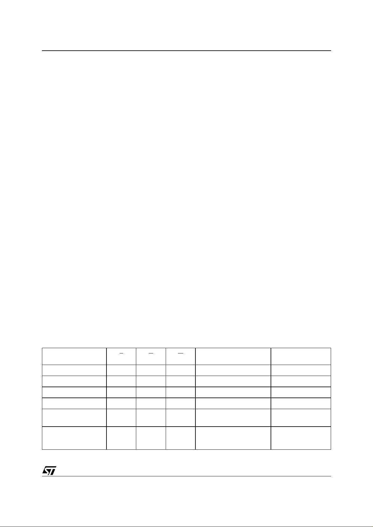
Table 5. Bus Operations
Operation E G W Add ress Inputs
Bus Read
Bus Write
Output Disable X
Standby
Read Manufacturer
Code
Read Device Code
Note: X = VIL or VIH.
Data
Inputs/Outp uts
V
IL
V
IL
V
IH
V
IL
V
IL
V
IL
V
IH
V
IH
X X X Hi-Z
V
IL
V
IL
V
V
V
V
V
Cell Address Data Output
IH
Command Address Data Input
IL
X Hi-Z
IH
A0 = VIL, A1 = VIL, A9 = VID,
IH
Others V
A0 = VIH, A1 = VIL, A9 = VID,
IH
Others V
IL
IL
or V
or V
IH
IH
B0h (M29F002BT)
B0h (M29F002BNT)
34h (M29F002BB)
20h
5/22
Page 6

M29F002BT, M29F002BB, M29F002BNT, M29F002BNB
COMMAND INTERFACE
All Bus Write operations t o the me mory are in terpreted by the Command Interface. Commands
consist of one or more sequential Bus Write operations. Failure to observe a valid sequence of Bus
Write operations will result in the memory returning to Read mode. The long command sequences
are imposed to maximize data security.
The commands are summarized in Table 6, Commands. Refer to Table 6 in conjunction with the
text descriptions below.
Read/Reset Command. The Read/Reset command returns the memory to its Read mode where
it behaves like a ROM or EPROM. It also resets
the errors in the Status Register. Either one or
three Bus Write operations can be u sed to issue
the Read/Reset command.
If the Read/Reset command is issued during a
Block Erase operation or following a Programming
or Erase error then the memory will take upto 10
µs
to abort. During the abort period no valid data can
be read from the mem ory. Issuing a Read/Reset
command during a Block Erase operation will
leave invalid data in the memory.
Auto Select Command. The Auto Select command is used to read the Manufacturer C ode, t he
Device Code and the Block Protection Status.
Three consecutive Bus Write operations are required to issue the Auto Select command. Once
the Auto Select comma nd is issued the memory
remains in Auto Select mode unt il another command is issued.
From the Auto Select mode the Manufacturer
Code can be read using a Bus Read operation
with A0 = V
may be set to either V
and A1 = VIL. The other address bits
IL
or VIH. The Manufa cturer
IL
Code for STMicroelectronics is 20h.
The Device Code can be read using a B us Read
operation with A0 = V
address bits may be set to e ither V
and A1 = VIL. The other
IH
or VIH. The
IL
Device Code for the M29F002BT is B0h, the
M29F002BNT is B0h and the M29F002BB is 34h.
The Block Protecti on St at us of e ac h bl ock can be
read using a Bus Rea d operation with A0 = V
A1 = V
, and A13-A17 specifying the address of
IH
IL
the block. The other address bits may be set to either V
or VIH. If the addressed block is protected
IL
then 01h is output on the Data Inputs/Outputs, otherwise 00h is output.
Program Command. The Program command
can be used to program a value to one address in
the memory array at a time. The command requires four Bus Write operations, the final write operation latches the address and data in the internal
state machine and starts the Program/Erase Controller.
If the address falls in a pro tected block then the
Program command is ignored, the data remains
unchanged. The Status Register is never read and
no error condition is given.
During the program operat ion the memo ry will ignore all commands. I t is n ot poss ible t o iss ue any
command to abort or pause the operation. Typical
program times are given in Table 7. Bus Read operations during the program o peration will output
the Status Register on the Data Inputs/Outputs.
See the section on the S tatus Register for more
details.
After the program operation has completed the
memory will return to the Read mode, unle ss an
error has occurred. When an error occurs the
memory will continue to output the Status Register. A Read/Reset command must be issued to reset the error condition and return to Read mode.
Note that the Program command cannot change a
bit set at ’0’ bac k to ’1’. One of the E rase Commands must be used to set all the bits in a block or
in the whole memory from ’0’ to ’1’.
Unlock Bypass Command. The Unlock Bypass
command is used in conjunction with the Unlock
Bypass Program command to program the memory. When the access time to the device is long (as
with some EPROM programmers) considerable
time saving can be made by using these commands. Three Bus Write operations are requ ired
to issue the Unlock Bypass command.
Once the Unlock Bypas s command has bee n issued the memory will only accept the Unloc k Bypass Program command and the Unlock Bypass
Reset command. The memory can be read as if in
Read mode.
Unlock Bypass Program Command. The Unlock Bypass Prog ram command can be u sed to
program one address in memory at a time. The
command requires two B us Write operations, the
final write operation latches the address and data
in the internal stat e machine and starts th e Program/Erase Controller.
,
The Program operation using the Unlock Bypass
Program command behaves identically to the Program operation using the Program command. A
protected block cannot be programmed; the operation cannot be aborted and the Status Register is
read. Errors must be reset using the Read/Re set
command, which l eaves the d evice in Unlo ck Bypass Mode. See the Program command for details
on the behavior.
6/22
Page 7
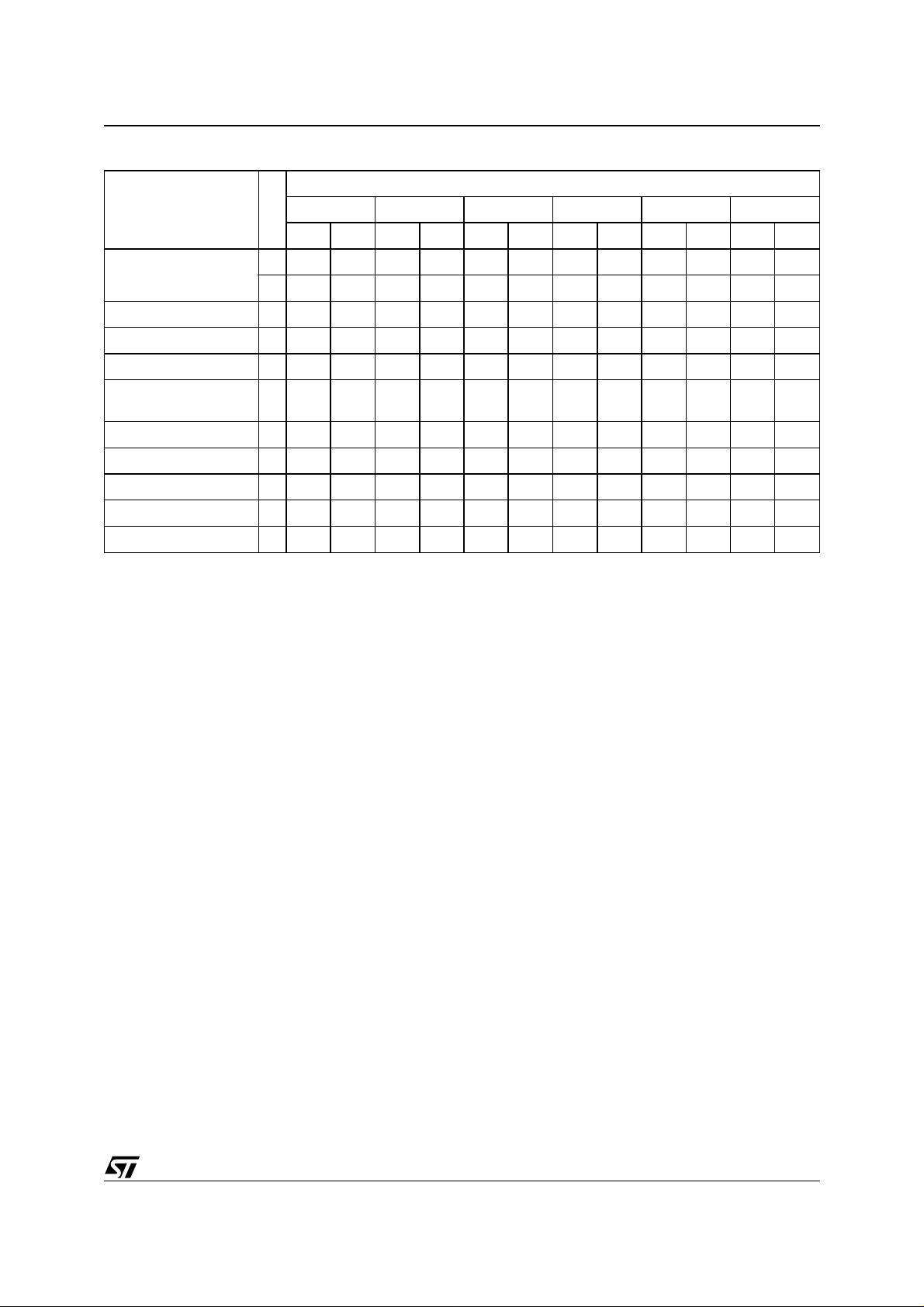
M29F002BT, M29F002BB, M29F 002BNT, M29F002BNB
Table 6. Commands
Bus Write Operations
Command
Read/Reset
Auto Select 3 555 AA 2AA 55 555 90
Program 4 555 AA 2AA 55 555 A0 PA PD
Unlock Bypass 3 555 AA 2AA 55 555 20
Unlock Bypass
Program
Unlock Bypass Reset 2 X 90 X 00
Chip Erase 6 555 AA 2AA 55 555 80 555 AA 2AA 55 555 10
Block Erase 6+ 555 AA 2AA 55 555 80 555 AA 2AA 55 BA 30
Erase Suspend 1 X B0
Erase Resume 1 X 30
Note: X Don’t Care, PA Program Address, PD Program Data, BA Any address in the Block.
All values in the table are in hexadecimal.
The Comman d Interface onl y uses address bi ts A 0-A10 to verify the commands , t he upper address bits are Don’ t C are.
Read/Re set. After a Read/Reset command, read the memory as normal until another command is issued.
Auto Select. After an Auto S el ect command, read Manufacturer ID, Device ID or Block Prot ection Status.
Program, Unlock Bypass Pr o g ram, Chip Erase, Block Eras e. After these comm ands rea d the S tatus Regist er until the P rogram /Erase
Controller completes a nd the memory ret urns to Read Mod e. Add additio nal Blocks durin g B l ock Erase Comm and with additional Bus Write
Operation s until the Time out Bit is set.
Unlock Bypass. After the Unlock Bypass command issue Unlock Bypass Program or Unlock Bypass Reset commands.
Unlock Bypass Reset. After the Unlock Bypass Reset command read the memory as normal until another command is issued.
Erase Suspend. After the Erase Suspend command read non-erasing memory blocks as normal, issue Auto Select and Program commands
on non-era sing blocks as normal.
Erase Resume. A fte r th e Er as e Res ume com man d th e sus pe nded Eras e o perat ion re sumes , re ad the Stat us R eg ister unt il t he Prog ram/
Erase Cont roller completes and the memory retur ns to Read Mode.
1X F0
3 555 AA 2AA 55 X F0
2X A0PAPD
1st 2nd 3rd 4th 5th 6th
Length
Addr Data Addr Data Addr Data Addr Data Addr Data Addr Data
Unlock Bypass Reset Command. The Unlock
Bypass Reset command can be used to return t o
Read/Reset mode from Unlock Bypass Mode.
Two Bus Write operations are required to issue the
Unlock Bypass Reset command.
Chip Erase Command. The Chip Erase command can be used to erase the entire chip. Six Bus
Write operations are required to issue the Chip
Erase Command and start the Program/Erase
Controller.
If any blocks are protected then these are ignored
and all the other blocks are erased. If all of the
blocks are protect e d th e Chip Erase op erat i on ap-
pears to start but will terminate within about 100µs,
leaving the data unchanged. No error condition is
given when protected blocks are ignored.
During the erase operation the memory will ignore
all commands. It is not possible to issue any command to abort the operation. Typical chip erase
times are given in Table 7. All Bus Read operations during the Chip E rase operation will output
the Status Register on the Data Inputs/Outputs.
See the section on the S tatus Register for more
details.
After the Chip Erase operation has completed t he
memory will return to the Read Mode, unle ss an
error has occurred. When an error occurs the
memory will continue to output the Status Register. A Read/Reset command must be issued to reset the error condition and return to Read Mode.
The Chip Erase Command sets all of the bits in unprotected blocks of the memory to ’1’. All previous
data is lost.
7/22
Page 8
M29F002BT, M29F002BB, M29F002BNT, M29F002BNB
Block Erase Command. The Block Erase com-
mand can be use d to erase a list of one or more
blocks. Six Bus Write operations are required to
select the first block in the list. Each additional
block in the list can be selected by repeating the
sixth Bus Write operation using the address of the
additional block. The Block Erase operation starts
the Program/Erase Controller about 50µs after the
last Bus Write operation. Once the Program/Erase
Controller starts it is not possible to select any
more blocks. Each additional block must therefore
be selected within 50µs of the last block. The 50µs
timer restarts when an additional block is selected.
The Status Register can be read after the sixth
Bus Write operation. See the Status Register for
details on how to identify if the Program/Erase
Controller has started the Block Erase operation.
If any selected blocks are protected then these are
ignored and all the other selected blocks are
erased. If all of the selected blocks are p rotected
the Block Erase operation appears to start but will
terminate within about 100µs, leaving the data unchanged. No error condition is given when protected blocks are ignored.
During the Block Erase operation the me mory wi ll
ignore all commands except the Erase Susp end
and Read/Reset commands. Typical block erase
times are given in Table 7. All Bus Read operations during the B lock E rase o peration will ou tput
the Status Register on the Data Inputs/Outputs.
See the section on the S tatus Register for more
details.
After the Block Erase operation has completed the
memory will return to the Read Mode, unle ss an
error has occurred. When an error occurs the
memory will continue to output the Status Regis-
ter. A Read/Reset command must be issued to reset the error condition and return to Read mode.
The Block Erase Command sets all of the bits in
the unprotected selected blocks to ’1’. All previous
data in the selected blocks is lost.
Erase Suspend Command. The Erase Suspend
Command may be used to temporarily suspend a
Block Erase operation and return the memory to
Read mode. The command requires one Bus
Write operation.
The Program/Erase Controller will sus pend within
15µs of the Erase Suspend Command being issued. Once the Program/Erase Controller has
stopped the memory will be set to Read mode and
the Erase will be suspended. If the Erase Suspend
command is issued during the period when the
memory is waiting for an additional block (before
the Program/Erase Controller starts) then the
Erase is suspended immediate ly and wi ll start immediately when the Erase Resume Comm and is
issued. It will not be possible to select any further
blocks for erasure after the Erase Resume.
During Erase Suspend it is possible to Read and
Program cells in blocks that are not being erased;
both Read and Program operations behave as
normal on these blocks. Reading from blocks that
are being erased will output the Status Register. It
is also possible to enter the Auto Select mode: the
memory will behave as in the Auto Select mode on
all blocks until a Read/Reset command returns the
memory to Erase Suspend mode.
Erase Resume Command. The Erase Resume
command must be used to restart the Program/
Erase Controller from Erase Suspend. An erase
can be suspended and resumed more than once.
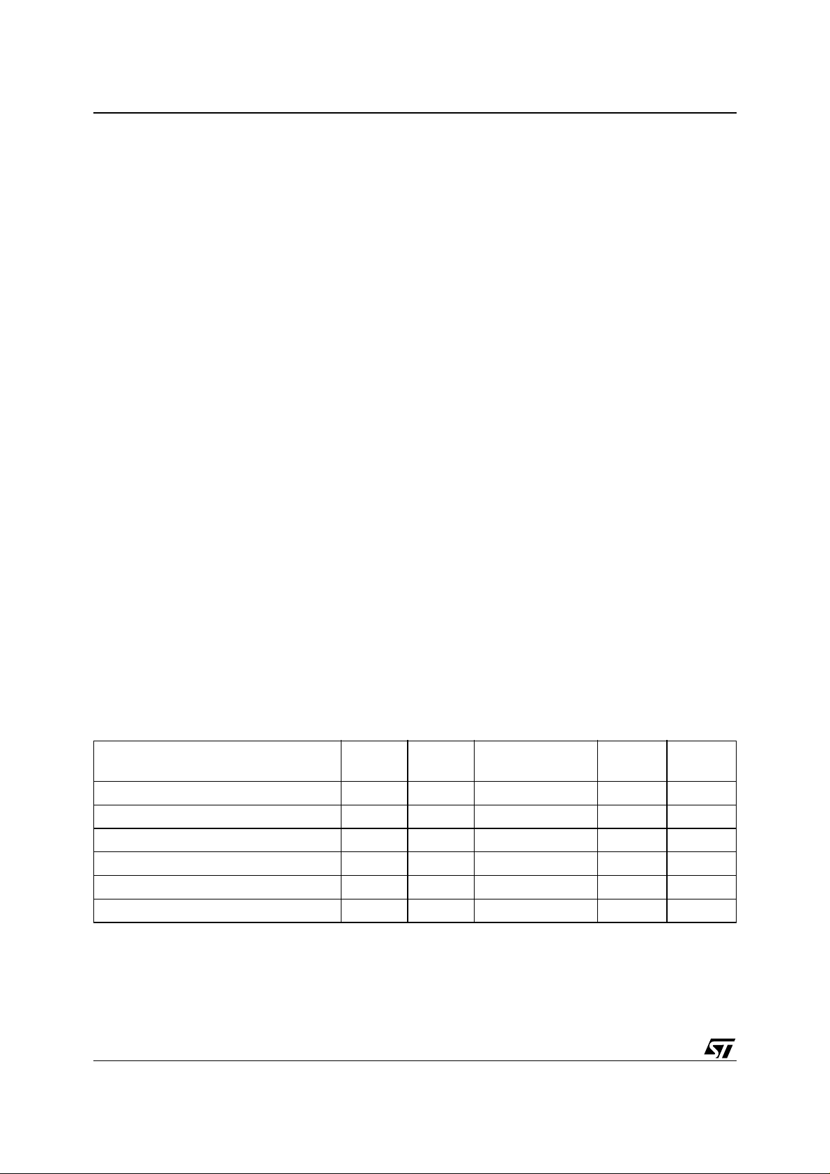
Table 7. Program, Erase Times and Progra m , Erase Endurance Cycles
= 0 to 70°C, –40 to 85°C or –40 to 125°C)
(T
A
Parameter Min
Chip Erase (All bits in the memory set to ‘0’) 0.8 0.8 sec
Chip Erase 2.5 2.5 10 sec
Block Erase (64 Kbytes) 0.6 0.6 4 sec
Program 8 8 150 µs
Chip Program 2.3 2.3 9 sec
Program/Erase Cycles (per Block) 100,000 cycles
Note: 1. TA = 25 °C, VCC = 5V.
8/22
Typ
(1)
Typical after
100k W/E Cycles
(1)
Max Unit
Page 9
M29F002BT, M29F002BB, M29F 002BNT, M29F002BNB
STATUS REGISTER
Bus Read operations from any address always
read the Status Register during Program and
Erase operations. It is also read during Erase Suspend when an address within a block being erased
is accessed.
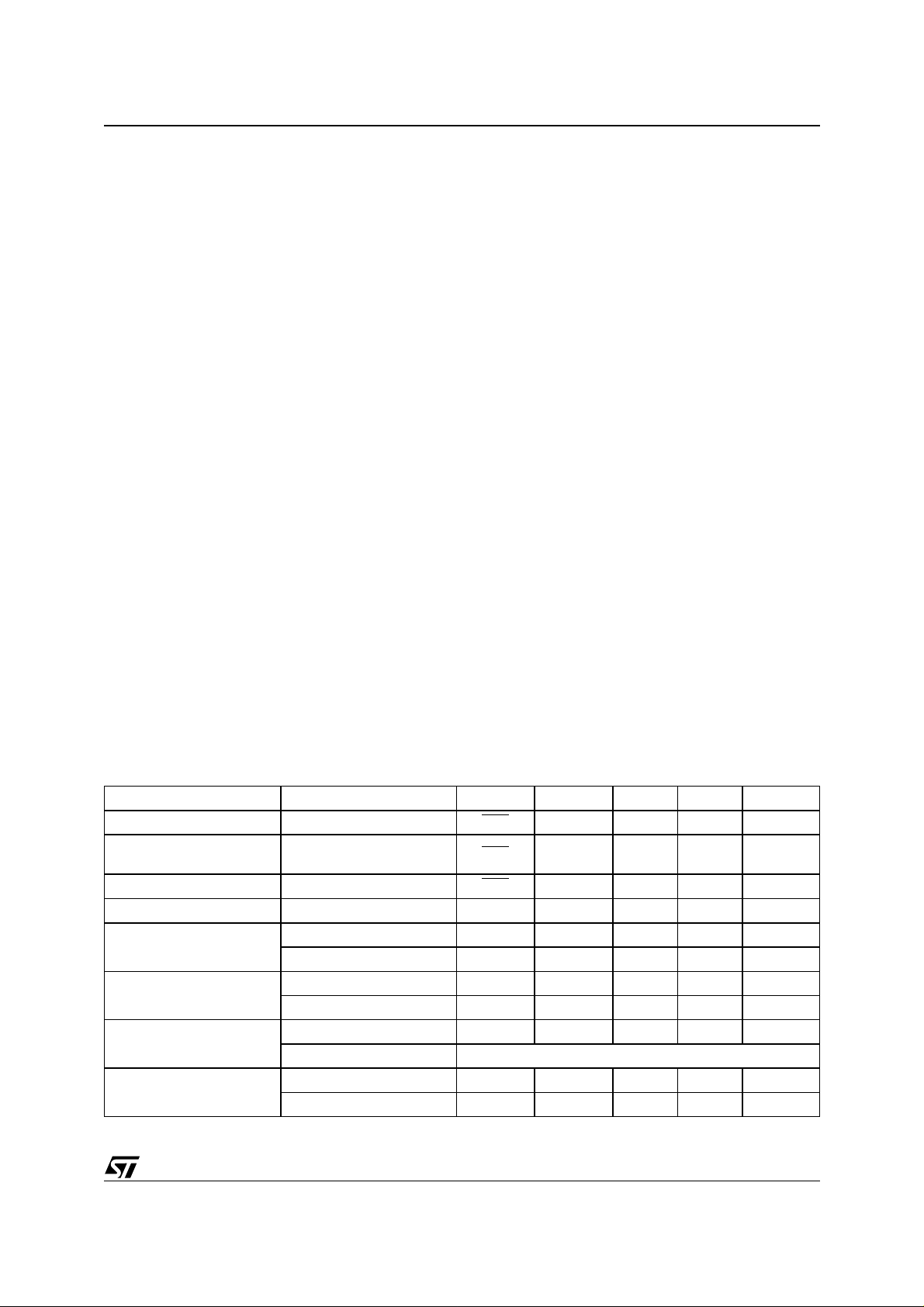
The bits in the Status Register are summarized in
Table 8, Status Register Bits.
Data Polling Bit (DQ7). The Data Polling Bit can
be used to identify whether the Program/Erase
Controller has successfully completed its operation or if it has responded to an Erase Suspend.
The Data Polling Bit is output on DQ7 when the
Status Register is read.
During Program operations the Data Polling Bit
outputs the complement of the bit being programmed to DQ7. After successful completion of
the Program operation the memory returns to
Read mode and Bus Read operations from the address just programmed o utput DQ7, not its complement.
During Er ase ope rations the Data Polling Bit ou t-
puts ’0’, the complement of the erased state of
DQ7. After successful completion of the Erase operation the memory returns to Read Mode.
In Erase Suspend mode the Data Polling Bit will
output a ’1’ during a Bus Read operation within a
block being erased. The Data Polling Bit will
change from a ’0’ to a ’1’ when the Program/Erase
Controller has suspended the Erase operation.
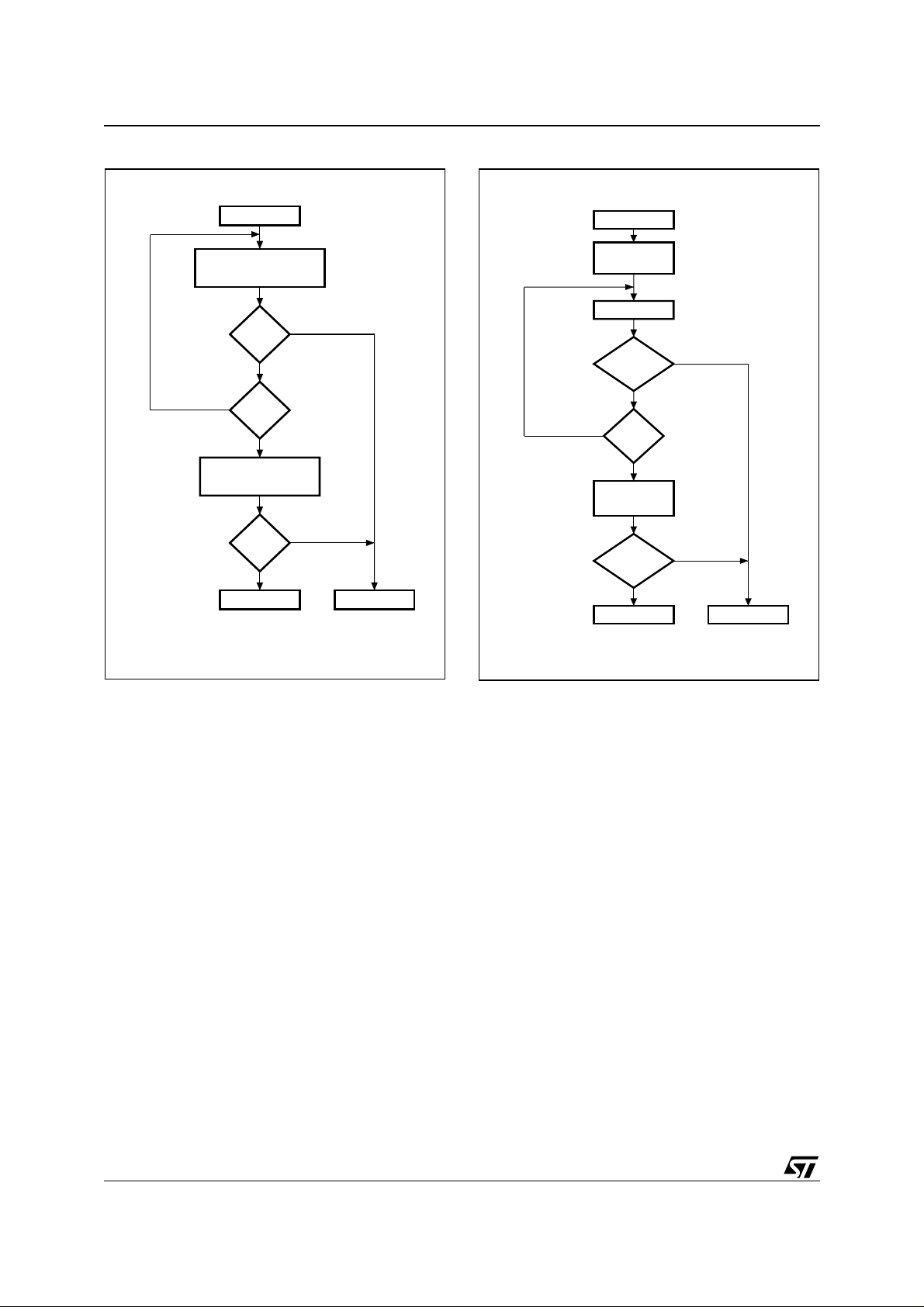
Figure 5, Data Polling Flowchart, gives an example of how to use the Data Polling Bit. A Valid Address is the address being programmed or an
address within the block being erased.
Toggle Bit (DQ6). The Togg le Bit can be used to
identify whether the Program/Erase Controller has
successfully completed its operation or if it has responded to an Erase Suspen d. The Toggle Bit is
output on DQ6 when the Status Register is read.
During Program and Erase operations the Toggle
Bit changes from ’0’ to ’ 1’ to ’ 0’, et c., with su ccessive Bus Read operations at any address. After
successful completion of the operation the memory returns to Read mode.
During Erase Suspend mode the Toggle Bit will
output when addressing a cell within a block being
erased. The Toggle Bit will stop toggling when the
Program/Erase Controller has suspended the
Erase operation.
Figure 6, Data Toggle Flowchart, g ives an example of how to use the Data Toggle Bit.
Error Bit (DQ5). The Error Bit can be used to
identify errors detected by the Program/Erase
Controller. The Error B it is set to ’1’ when a Program, Block Erase or Chip Erase operation fails to
write the correct data to the memory. If the Error
Bit is set a Read/Rese t command must be issued
before other commands are issued. The E rror bit
is output on DQ5 when the Status Register is read.
Note that the Program command cannot change a
bit set at ’0’ back to ’1’ and attempting to do so may
or may not set DQ5 at ’1’. In both cases, a successive Bus Read operation will show the bit is still ’0’.
One of the Erase commands must be used to set
all the bits in a block or in the whole memory from
’0’ to ’1’.
Table 8. Status Register Bits
Operation Address DQ7 DQ6 DQ5 DQ3 DQ2
Program Any Address DQ7
Program During Erase
Suspend
Program Error Any Address DQ7
Chip Erase Any Address 0 Toggle 0 1 Toggle
Block Erase before timeout
Block Erase
Erase Suspend
Erase Error
Note: Unspecifi ed data bits should be ignore d.
Any Address DQ7
Erasing Block 0 Toggle 0 0 Toggle
Non-Erasing Block 0 Toggle 0 0 No Toggle
Erasing Block 0 Toggle 0 1 Toggle
Non-Erasing Block 0 Toggle 0 1 No Toggle
Erasing Block 1 No Toggle 0 – Toggle
Non-Erasing Block Data read as normal
Good Block Address 0 Toggle 1 1 No Toggle
Faulty Block Address 0 Toggle 1 1 Toggle
Toggle 0 ––
Toggle 0 – –
Toggle 1 – –
9/22
Page 10
M29F002BT, M29F002BB, M29F002BNT, M29F002BNB
Figure 5. Dat a Po ll i ng Fl o wc h a rt
START
READ DQ5 & DQ7
at VALID ADDRESS
DQ7
DATA
NO
DQ5
READ DQ7
at VALID ADDRESS
DQ7
DATA
FAIL PASS
= 1
YES
=
NO
YES
YES
=
NO
AI03598
Figure 6. Dat a Toggle Flowcha rt
START
READ
DQ5 & DQ6
READ DQ6
DQ6
=
TOGGLE
NO
DQ5
= 1
READ DQ6
TWICE
DQ6
=
TOGGLE
FAIL PASS
NO
YES
YES
NO
YES
AI01370B
Erase Timer Bit (DQ3). The Erase Timer Bit can
be used to identify the start of Program/Erase
Controller operation during a Block Erase command. Once the Program/Erase Controller starts
erasing the Erase Timer Bit is set to ’1’. Before the
Program/Erase Controller starts the Erase Timer
Bit is set to ’0’ and additional block s to be erased
may be written to the Command Interface. The
Erase Timer Bit is output on DQ3 when the Status
Register is read.
Alternative Toggle Bit (DQ2). The Alternative
Toggle Bit can be used to monitor the Program/
Erase controller during Erase operations. The Alternative Toggle Bit is output on DQ2 when the
Status Register is read.
During Chip Erase and Block Erase operations the
Toggle Bit changes from ’0’ to ’1’ to ’0’, etc., with
successive Bus Read operations from addresses
10/22
within the blocks being erased. Once t he operatio n
completes the memory returns to Read mode.
During Erase Suspend the Alternative Toggle Bit
changes from ’0’ to ’1’ to ’0’, etc. with successive
Bus Read operations from addresses within the
blocks being erased. Bus Read operations to addresses within blocks not being erased will ou tput
the memory cell data as if in Read mode.
After an Erase operation that c auses t he Error Bit
to be set the Alternative Toggle Bit can be used to
identify which block or blocks have caused the error. The Alternative Toggle Bit changes from ’0’ to
’1’ to ’0’, etc. with successive Bus Re ad Operations from addresses within blocks that have not
erased correctly. The Alternative Togg le Bit does
not change if the addressed block has erased correctly.
Page 11
M29F002BT, M29F002BB, M29F 002BNT, M29F002BNB
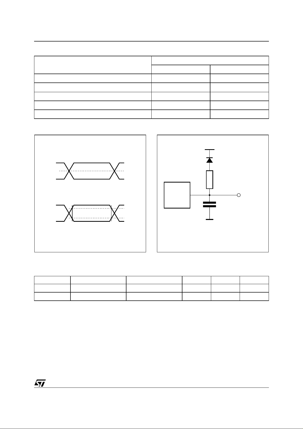
Table 9. AC Measurement Conditions
Parameter
45 / 55 70 / 90 / 120
AC Test Conditions High Speed Standard
M29F002B
Load Capacitance (C
Input Rise and Fall Times
)
L
30pF 100pF
10ns
≤
10ns
≤
Input Pulse Voltages 0 to 3V 0.45 to 2.4V
Input and Output Timing Ref. Voltages 1.5V 0.8V and 2V
Figure 7. AC Testing Input Output Waveform
High Speed
3V
1.5V
0V
Standard
2.4V
0.45V
2.0V
0.8V
AI01275B
Figure 8. AC Tes t i ng Load Circuit
1.3V
1N914
3.3kΩ
DEVICE
UNDER
TEST
CL = 30pF or 100pF
OUT
CL includes JIG capacitance
Table 10. Capacitance
(T
= 25 °C, f = 1 MHz)
A
Symbol Parameter Test Condition Min Max Unit
V
V
IN
OUT
= 0V
= 0V
6pF
12 pF
C
IN
C
OUT
Note: Sampled on l y, not 100% tested.
Input Capacitance
Output Capacitance
AI03027
11/22
Page 12
M29F002BT, M29F002BB, M29F002BNT, M29F002BNB
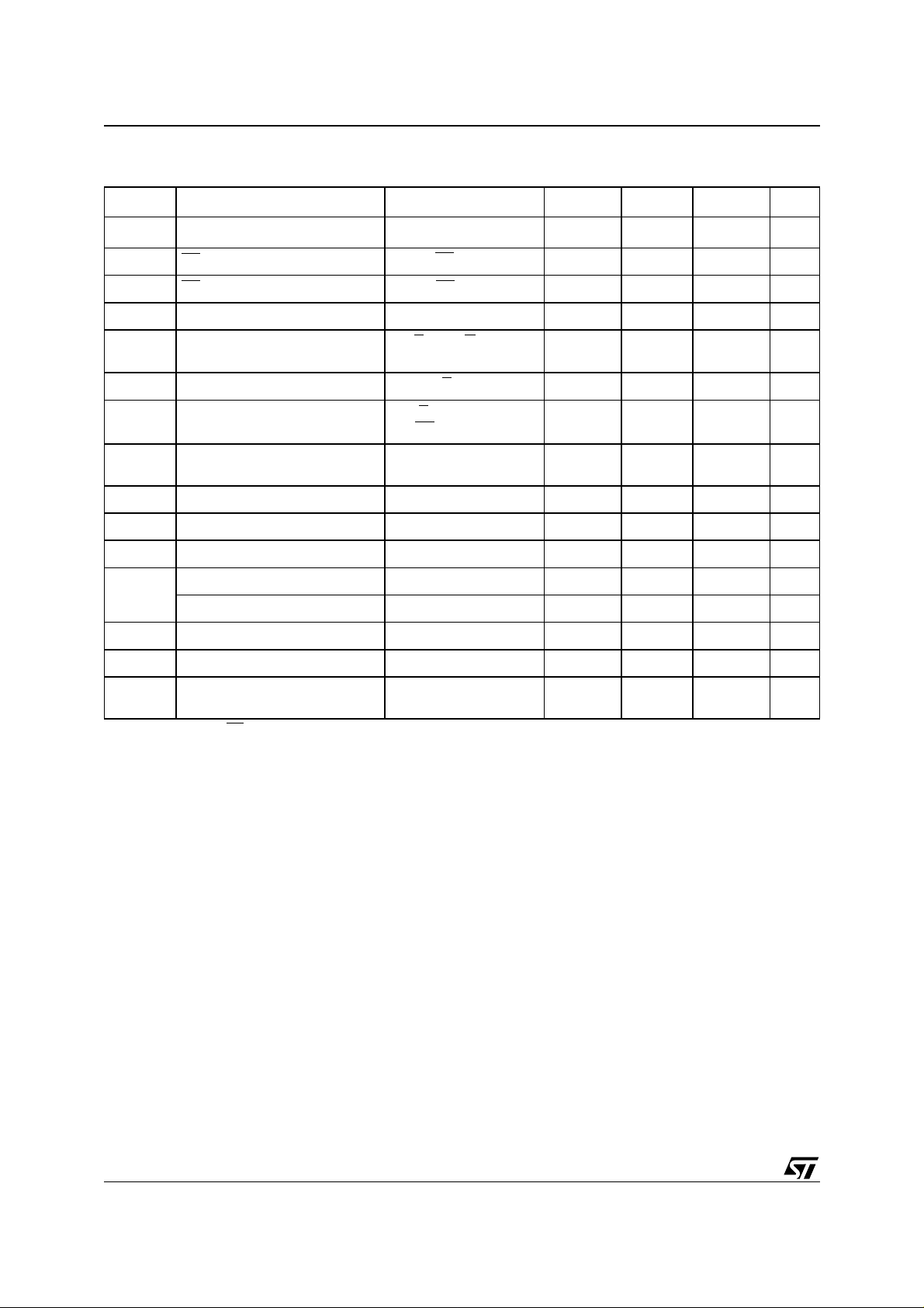
Table 11. DC Characteristics
(T
= 0 to 70°C, –40 to 85°C or –40 to 125°C)
A
Symbol Parameter Test Condition Min
(1)
I
LI
I
LR1
I
LR2
I
LO
I
CC1
I
CC2
I
CC3
Input Leakage Current
RP Leakage Current High
RP Leakage Current Low
Output Leakage Curren t
Supply Current (Read)
Supply Current (Standby) TTL
Supply Current (Standby) CMOS
0V ≤ V
0V ≤ V
E
≤ V
IN
RP
= V
CC
RP
= V
SS
≤ V
OUT
= VIL, G = VIH,
f = 6MHz
E
= V
IH
E
= VCC ±0.2V,
RP
= VCC ±0.2V
CC
CC
Typ
(3)
Max Unit
±1 µA
±1 µA
–0.2 –10 µA
±1 µA
515mA
1mA
30 100 µA
(2)
I
CC4
V
V
V
Supply Current (Program/Eras e)
Input Low Voltage –0.5 0.8 V
IL
Input High Voltage 2
IH
Output Low Voltage
OL
Output High Voltage TTL
V
OH
V
I
V
LKO
Note: 1. Excludi ng the RP i nput.
Output High Voltage CMOS
Identification Voltage 11.5 12.5 V
ID
Identification Current
ID
Program/Erase Lockout Supply
(2)
Voltage
2. Sampled only, not 100% tested.
3. T
= 25°C, VCC = 5V.
A
Program/Erase
Controller active
I
= 5.8mA
OL
I
= –12.5mA
OH
I
= –100µA VCC –0.4
OH
A9 = V
ID
20 mA
V
+0.5
CC
0.45 V
2.4 V
100 µA
3.2 4.2 V
V
V
12/22
Page 13
M29F002BT, M29F002BB, M29F 002BNT, M29F002BNB
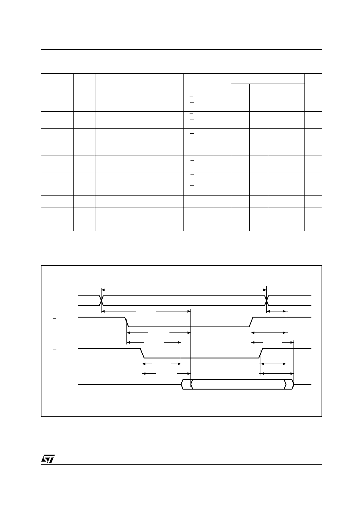
Table 12. Read AC Characteristics
(TA = 0 to 70°C, –40 to 85°C or –40 to 125°C)
Symbol Alt Parameter Test Condition
E
= VIL,
G
= V
E
= VIL,
G
= V
= V
G
G
= V
= V
E
E
= V
G
= V
E
= V
IL
IL
IL
IL
IL
IL
IL
IL
(1)
t
Address Valid to Next Address Valid
RC
t
Address Valid to Output Valid
ACC
Chip Enable Low to Output
t
LZ
Transition
t
Chip Enable Low to Output Valid
CE
Output Enable Low to Output
t
OLZ
Transition
t
Output Enable Low to Output Valid
OE
t
Chip Enable High to Output Hi-Z
HZ
t
Output Enable High to Output Hi-Z
DF
Chip Enable, Output Enable or
t
Address Transition to Output
OH
Transition
t
AVAV
t
AVQV
(1)
t
ELQX
t
ELQV
(1)
t
GLQX
t
GLQV
(1)
t
EHQZ
t
GHQZ
t
EHQX
t
GHQX
t
AXQX
Note: 1. Sampled only, not 100% tested.
M29F002B
Unit
45 55 70 / 90 / 120
Min 45 55 70 ns
Max 45 55 70 ns
Min 0 0 0 ns
Max 45 55 70 ns
Min 0 0 0 ns
Max 25 30 30 ns
Max 15 18 20 ns
Max 15 18 20 ns
Min 0 0 0 ns
Figure 9. Read Mode AC Waveforms
A0-A17
tAVQV tAXQX
E
G
DQ0-DQ7
tAVAV
VALID
tELQV tEHQX
tELQX tEHQZ
tGLQX tGHQX
tGLQV
tGHQZ
VALID
AI02961
13/22
Page 14
M29F002BT, M29F002BB, M29F002BNT, M29F002BNB
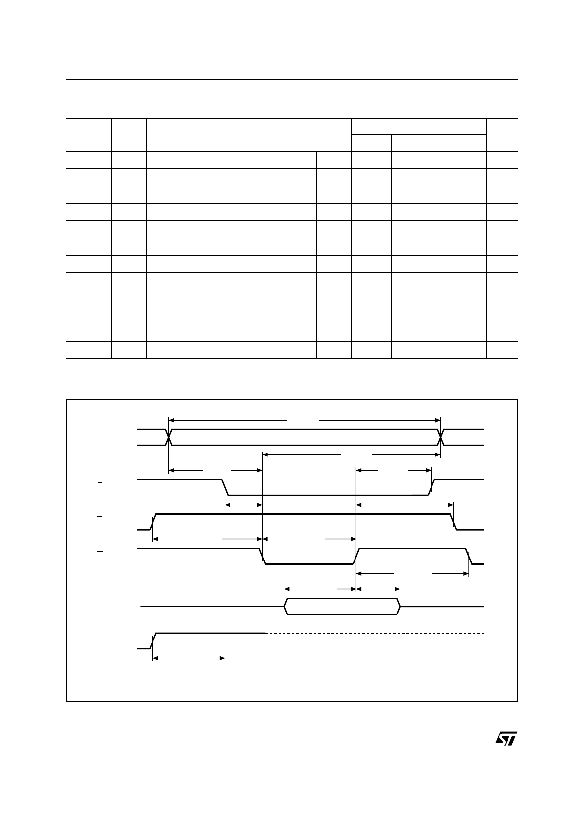
Table 13. Write AC Characteristics, Write Enable Controlled
(T
= 0 to 70°C, –40 to 85°C or –40 to 125°C)
A
Symbol Alt Parameter
t
AVAV
t
ELWL
t
WLWH
t
DVWH
t
WHDX
t
WHEH
t
WHWL
t
AVWL
t
WLAX
t
GHWL
t
WHGL
t
VCHEL
t
Address Valid to Next Address Valid Min 45 55 70 ns
WC
t
Chip Enable Low to Write Enable Low Min 0 0 0 ns
CS
t
Write Enable Low to Write Enable High Min 40 40 45 ns
WP
t
Input Valid to Write Enable High Min 25 25 30 ns
DS
t
Write Enable High to Input Transition Min 0 0 0 ns
DH
t
Write Enable High to Chip Enable High Min 0 0 0 ns
CH
t
Write Enable High to Write Enable Low Min 20 20 20 ns
WPH
t
Address Valid to Write Enable Low Min 0 0 0 ns
AS
t
Write Enable Low to Address Transition Min 40 40 45 ns
AH
Output Enable High to Write Enable Low Min 0 0 0 ns
t
Write Enable High to Output Enable Low Min 0 0 0 ns
OEH
t
VCSVCC
High to Chip Enable Low
Min 50 50 50 µs
M29F002B
Unit
45 55 70 / 90 / 120
Figure 10. Write AC Waveforms, Write Enable Controlled
tAVAV
A0-A17
E
G
W
DQ0-DQ7
V
CC
tAVWL
tELWL
tVCHEL
VALID
tWLWHtGHWL
tDVWH
tWLAX
tWHEH
tWHGL
tWHWL
tWHDX
VALID
AI02083
14/22
Page 15
M29F002BT, M29F002BB, M29F 002BNT, M29F002BNB
Table 14. Write AC Characteristics, Chip Enable Controlled
(T
= 0 to 70°C, –40 to 85°C or –40 to 125°C)
A
Symbol Alt Parameter
t
AVAV
t
WLEL
t
ELEH
t
DVEH
t
EHDX
t
EHWH
t
EHEL
t
AVEL
t
ELAX
t
GHEL
t
EHGL
t
VCHWL
t
Address Valid to Next Address Valid Min 45 55 70 ns
WC
t
Write Enable Low to Chip Enable Low Min 0 0 0 ns
WS
t
Chip Enable Low to Chip Enable High Min 40 40 45 ns
CP
t
Input Valid to Chip Enable High Min 25 25 30 ns
DS
t
Chip Enable High to Input Transition Min 0 0 0 ns
DH
t
Chip Enable High to Write Enable High Min 0 0 0 ns
WH
t
Chip Enable High to Chip Enable Low Min 20 20 20 ns
CPH
t
Address Valid to Chip Enable Low Min 0 0 0 ns
AS
t
Chip Enable Low to Address Transition Min 40 40 45 ns
AH
Output Enable High Chip Enable Low Min 0 0 0 ns
t
Chip Enable High to Output Enable Low Min 0 0 0 ns
OEH
t
VCSVCC
High to Write Enable Low
Min 50 50 50 µs
M29F002B
Unit
45 55 70 / 90 / 120
Figure 11. Write AC Waveforms, Chip Enable Controlled
tAVAV
A0-A17
W
G
E
DQ0-DQ7
V
CC
tAVEL
tWLEL
tVCHWL
VALID
tELEHtGHEL
tDVEH
tELAX
tEHWH
tEHGL
tEHEL
tEHDX
VALID
AI02084
15/22
Page 16
M29F002BT, M29F002BB, M29F002BNT, M29F002BNB
Table 15. Reset/Block Temporary Unprotect AC Characteristics
(TA = 0 to 70°C, –40 to 85°C or –40 to 125°C)
Symbol Alt Parameter
(1)
t
PHWL
t
PHEL
(1)
t
PHGL
t
PLPX
(1)
t
PLYH
t
PHPHH
Note: 1. Sampled only, not 100% tested.
t
(1)
READY
t
Figure 12. Reset/Block Temporary Unprotect AC Waveforms
RP High to Write Enable Low, Chip Enable
t
RH
Low, Output Enable Low
t
RP Pulse Width Min 500 500 500 ns
RP
Min 50 50 50 ns
RP Low to Read Mode Max 10 10 10 µs
RP Rise Time to V
VIDR
ID
Min 500 500 500 ns
M29F002B
Unit
45 55 70 / 90 / 120
W,
RP
E, G
tPHWL, tPHEL, tPHGL
tPLPX
tPHPHH
tPLYH
AI02943
16/22
Page 17

M29F002BT, M29F002BB, M29F 002BNT, M29F002BNB
Table 16. Ordering Information Scheme
Example: M29F002BB 45 N 1 T
Device Type
M29
Operating Voltage
F = V
Device Function
002B = 2 Mbit (256Kb x8), Boot Block
Array Matrix
T = Top Boot
B = Bottom Boot
NT = Top Boot, No Reset/Block Temporary Unprotect pin
NB = Bottom Boot, No Reset/Block Temporary Unprotect pin
Speed
45 = 45 ns
55 = 55 ns
70 = 70 ns
90 = 90 ns
120 = 120 ns
= 5V ± 10%
CC
Package
K = PLCC32
N = TSOP32: 8 x 20 mm
P = PDIP32
Temperature Range
1 = 0 to 70 °C
6 = –40 to 85 °C
3 = –40 to 125 °C
Option
T = Tape & Reel Packing
Note: The last two characters o f the ordering code m ay be replaced by a letter code for preprogramm ed
parts, otherwise devices are shipped from the factory with the memory content bits erased to ’1’.
For a list of available options (Speed, Pac kage, etc...) or for furthe r information on any aspect of this device, please contact the ST Sales Office nearest to you.
17/22
Page 18

M29F002BT, M29F002BB, M29F002BNT, M29F002BNB
Table 17. Revision History
Date Rev. Revision Details
July 1999 -01 First Issue
Chip Erase Max. specification added (Table 7)
Block Erase Max. specification added (Table 7)
07-Oct-1999 -02
28-Jul-2000 -03
22-Apr-2002 -04
Program Max. specification added (Table 7)
Chip Program Max. specification added (Table 7)
and I
I
CC1
I
Test Condition changed (Table 11)
CC3
Typ. specification added (Table 11)
CC3
New document template
Document type: from Preliminary Data to Data Sheet
Status Register bit DQ5 clarification
Data Polling Flowchart diagram change (Figure 5)
Data Toggle Flowchart diagram change (Figure 6)
M29F002BNB device added
PLCC32 package mechanica l data modified
18/22
Page 19
M29F002BT, M29F002BB, M29F 002BNT, M29F002BNB
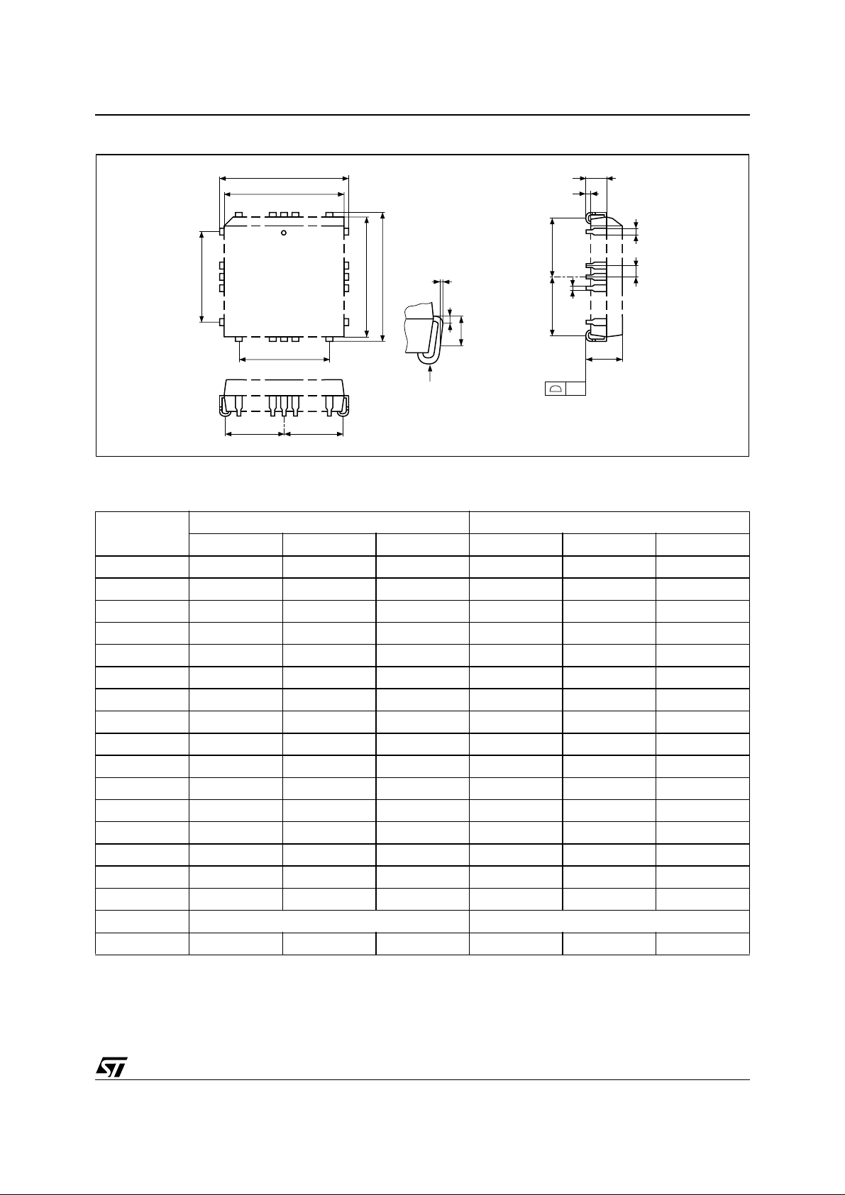
PLCC32 – 32 lead Plastic Leaded Chip Carrier, Package Outline
E3
Note: Drawing is not to scale.
D
D1
1 N
D3
D2 D2
E1 E
F
0.51 (.020)
1.14 (.045)
R
A1
A2
B1
E2
e
B
E2
A
CP
PLCC-A
PLCC32 – 32 lead Plastic Leaded Chip Carrier, Package Mechanical Data
Symbol
Typ Min Max Typ Min Max
A 3.18 3.56 0.125 0.140
A1 1.53 2.41 0.060 0.095
A2 0.38 – 0. 015 –
B 0.33 0.53 0.013 0.021
B1 0.66 0.81 0.026 0.032
CP 0.10 0.004
D 12.32 12.57 0.485 0.495
D1 11.35 11.51 0.447 0.453
D2 4.78 5.66 0.188 0.223
D3 7.62 – – 0.300 – –
E 14.86 15.11 0.585 0.595
E1 13.89 14.05 0.547 0.553
E2 6.05 6.93 0.238 0.273
E3 1 0.16 – – 0.400 – –
e 1.27 – – 0.050 – –
F 0.00 0.13 0.000 0.005
N32 32
R 0.89 – – 0.035 – –
millimeters inches
19/22
Page 20
M29F002BT, M29F002BB, M29F002BNT, M29F002BNB
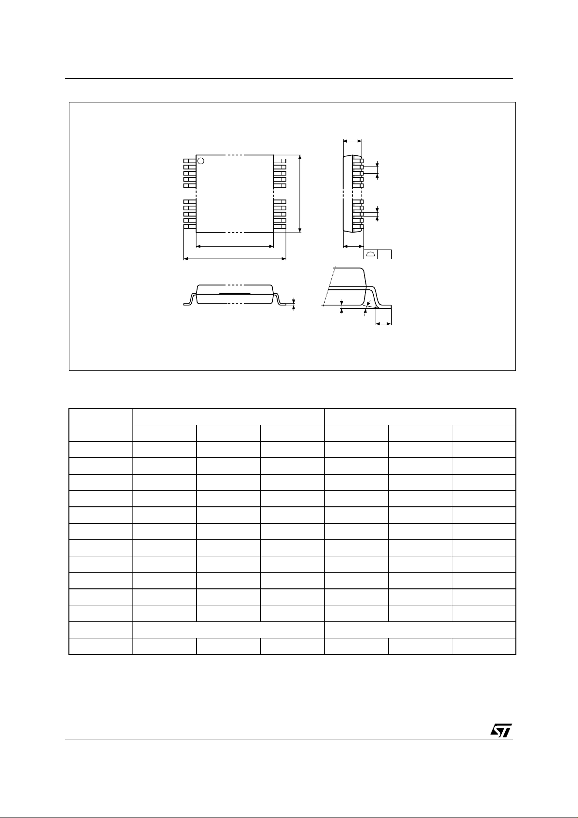
TSOP32 – 32 lead Plastic Thin Small Outline, 8 x 20mm, Packag e Outline
A2
Note: Drawing is not to scale.
1 N
N/2
TSOP-a
D1
D
DIE
E
A
C
e
B
CP
LA1 α
TSOP32 – 32 lead Plastic Thin Small Outline, 8 x 20mm, Packag e Mechanical Data
Symbol
Typ Min Max Typ Min Max
A 1.20 0.0472
millimeters inches
20/22
A1 0.05 0.15 0.0020 0.0059
A2 0.95 1.05 0.0374 0.0413
B 0.15 0.27 0.0059 0.0106
C 0.10 0.21 0.0039 0.0083
D 19.80 20.20 0.7795 0.7953
D1 18.30 18.50 0.7205 0.7283
E 7.90 8.10 0.3110 0.3189
e 0.50 – – 0.0197 – –
L 0.50 0.70 0.0197 0.0276
α
0° 5° 0° 5°
N32 32
CP 0.10 0.0039
Page 21
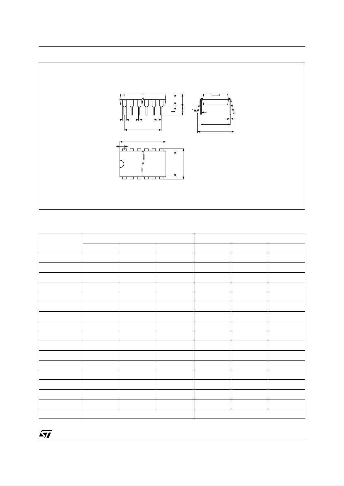
M29F002BT, M29F002BB, M29F 002BNT, M29F002BNB
PDIP32 - 32 lead Plastic DIP, 600 mils width, Package Outline
A2
A1AL
B1 B e1
D2
D
S
N
E1 E
1
Note: 1. Drawing is not to scale.
α
C
eA
eB
PDIP
PDIP32 - 32 lead Plastic DIP, 600 mils width, Package Mechanical Data
Symb.
Typ. Min. Max. Typ. Min. Max.
A – 5.08 – 0.2000
A1 0.38 – 0.0150 –
A2 3.56 4.06 0.1402 0.1598
B 0.38 0 .51 0.0150 0.0201
mm inches
B1 1.52 – – 0.0598 – –
C 0.20 0.30 0.0079 0.0118
D 41.78 42.04 1.6449 1.6551
D2 3 8.10 – – 1.5000 – –
E 15.24 – – 0.6000 – –
E1 13.59 13.84 0.5350 0.5449
e1 2.54 – – 0.1 000 – –
eA 15.24 – – 0.6000 – –
eB 15.24 17.78 0.6000 0.7000
L 3.18 3.43 0.1252 0.1350
S 1.78 2 .03 0.0701 0.0799
α
0° 10° 0° 10°
N32 32
21/22
Page 22

M29F002BT, M29F002BB, M29F002BNT, M29F002BNB
Information furnishe d is bel i eved to be accurate and reliable. However, STMicroelectroni cs assumes no responsibility for the consequences
of use of such information nor for any infringement of patents or other rights of third parties which may result from its use. No license is granted
by implic ation or otherwise unde r any patent or patent rights of STMicroelectronics. Speci fications me ntioned in th i s publication are subject
to change without notice. This publication supersedes and replaces all information previously supplied. STMicroelectronics produ ct s are not
authorized for use as crit i cal component s in l i fe support dev i ces or systems without expre ss written appr oval of STMicro el ectronics.
The ST log o i s registered trademark of STM i croelectronics
All other nam es are the property of their respective owners
© 2002 STMicroelectronics - All Rights Reserved
STMicroelectronics group of companies
Austra lia - Brazil - Canada - China - Finland - France - Germ any - Hong Kong -
India - Israel - Italy - Japan - Malaysi a - M al ta - Morocco - Singapore - Spai n - Sweden - Switz erland - United Kingdom - United States.
www.st.com
22/22
 Loading...