

Page 1

1/50March 2003
M28R400CT
M28R400CB
4 Mbit (256Kb x16, Boot Block)
1.8V Supply Flash Memory
FEATURES SUMMARY
■ SUPPLY VOLTAGE
–V
DD
= 1.65V to 2.2V Core Power Supply
–V
DDQ
= 1.65V to 2.2V for Input/Output
–V
PP
= 12V for fast Program (optional)
■ ACCESS TIMES: 90ns, 120ns
■ PROGRAMMING TIME
– 10µs typic al
– Double Word Programming Option
■ COMMON FLASH INTERFACE
– 64 bit Security Code
■ MEMORY BLOCKS
– Parameter Blo cks (Top or Bottom location)
– Main Blocks
■ BLOCK LOCKING
– All blocks locked at Power Up
– Any combination of blocks can be locked
–WP
for Block Lock-Down
■ SECURITY
– 64 bit user Programmable OTP cells
– 64 bit unique device identifier
– One Parameter Block Permanently Lockable
■ AUTOMATIC STAND-BY MODE
■ PROGRAM and ERASE SUSPEND
■ 100,000 PROGRAM/ER ASE CYCL ES per
BLOCK
■ ELECTRONIC SIGNATURE
– Manufacturer Code: 20h
– Top Device Code, M28R400CT: 882Ah
– Bottom Device Code, M28R400CB: 882Bh
Figure 1. Packages
FBGA
TFBGA46 (ZB)
6.39 x 6.37mm
Page 2

M28R400CT, M28R400CB
2/50
TABLE OF CONTENTS
SUMMARY DESCRIPTION. . . . . . . . . . . . . . . . . . . . . . . . . . . . . . . . . . . . . . . . . . . . . . . . . . . . . . . . . . . 5
Figure 2. Logic Diagram . . . . . . . . . . . . . . . . . . . . . . . . . . . . . . . . . . . . . . . . . . . . . . . . . . . . . . . . . . 5
Table 1. Signal Names . . . . . . . . . . . . . . . . . . . . . . . . . . . . . . . . . . . . . . . . . . . . . . . . . . . . . . . . . . . 5
Figure 3. TFBGA Connections (Top view through package). . . . . . . . . . . . . . . . . . . . . . . . . . . . . . . 6
Figure 4. Block Addresses. . . . . . . . . . . . . . . . . . . . . . . . . . . . . . . . . . . . . . . . . . . . . . . . . . . . . . . . . 7
Figure 5. Security Block Memory Map. . . . . . . . . . . . . . . . . . . . . . . . . . . . . . . . . . . . . . . . . . . . . . . . 7
SIGNAL DESCRIPTIONS . . . . . . . . . . . . . . . . . . . . . . . . . . . . . . . . . . . . . . . . . . . . . . . . . . . . . . . . . . . . 8
Address Inputs (A0-A17). . . . . . . . . . . . . . . . . . . . . . . . . . . . . . . . . . . . . . . . . . . . . . . . . . . . . . . . . . 8
Data Input/Output (DQ0-DQ15). . . . . . . . . . . . . . . . . . . . . . . . . . . . . . . . . . . . . . . . . . . . . . . . . . . . . 8
Chip Enable (E). . . . . . . . . . . . . . . . . . . . . . . . . . . . . . . . . . . . . . . . . . . . . . . . . . . . . . . . . . . . . . . . . 8
Output Enable (G). . . . . . . . . . . . . . . . . . . . . . . . . . . . . . . . . . . . . . . . . . . . . . . . . . . . . . . . . . . . . . . 8
Write Enable (W). . . . . . . . . . . . . . . . . . . . . . . . . . . . . . . . . . . . . . . . . . . . . . . . . . . . . . . . . . . . . . . . 8
Write Protect (WP). . . . . . . . . . . . . . . . . . . . . . . . . . . . . . . . . . . . . . . . . . . . . . . . . . . . . . . . . . . . . . .8
Reset (RP). . . . . . . . . . . . . . . . . . . . . . . . . . . . . . . . . . . . . . . . . . . . . . . . . . . . . . . . . . . . . . . . . . . . . 8
V
DD
Supply Voltage (1.65V to 2.2V) . . . . . . . . . . . . . . . . . . . . . . . . . . . . . . . . . . . . . . . . . . . . . . . . .8
V
DDQ
Supply Voltage (1.65V to 2.2V). . . . . . . . . . . . . . . . . . . . . . . . . . . . . . . . . . . . . . . . . . . . . . . . 8
V
PP
Program Supply Voltage . . . . . . . . . . . . . . . . . . . . . . . . . . . . . . . . . . . . . . . . . . . . . . . . . . . . . . 8
V
SS
Ground. . . . . . . . . . . . . . . . . . . . . . . . . . . . . . . . . . . . . . . . . . . . . . . . . . . . . . . . . . . . . . . . . . . . 8
BUS OPERATIONS. . . . . . . . . . . . . . . . . . . . . . . . . . . . . . . . . . . . . . . . . . . . . . . . . . . . . . . . . . . . . . . . . 9
Read.. . . . . . . . . . . . . . . . . . . . . . . . . . . . . . . . . . . . . . . . . . . . . . . . . . . . . . . . . . . . . . . . . . . . . . . . . 9
Write.. . . . . . . . . . . . . . . . . . . . . . . . . . . . . . . . . . . . . . . . . . . . . . . . . . . . . . . . . . . . . . . . . . . . . . . . . 9
Output Disable. . . . . . . . . . . . . . . . . . . . . . . . . . . . . . . . . . . . . . . . . . . . . . . . . . . . . . . . . . . . . . . . . . 9
Standby. . . . . . . . . . . . . . . . . . . . . . . . . . . . . . . . . . . . . . . . . . . . . . . . . . . . . . . . . . . . . . . . . . . . . . . 9
Automatic Standby. . . . . . . . . . . . . . . . . . . . . . . . . . . . . . . . . . . . . . . . . . . . . . . . . . . . . . . . . . . . . . . 9
Reset. . . . . . . . . . . . . . . . . . . . . . . . . . . . . . . . . . . . . . . . . . . . . . . . . . . . . . . . . . . . . . . . . . . . . . . . . 9
Read Electronic Signature Comma nd . . . . . . . . . . . . . . . . . . . . . . . . . . . . . . . . . . . . . . . . . . . . . . . 10
Table 2. Bus Operations . . . . . . . . . . . . . . . . . . . . . . . . . . . . . . . . . . . . . . . . . . . . . . . . . . . . . . . . . . 9
COMMAND INTERFACE . . . . . . . . . . . . . . . . . . . . . . . . . . . . . . . . . . . . . . . . . . . . . . . . . . . . . . . . . . . 10
Read Memory Array Command. . . . . . . . . . . . . . . . . . . . . . . . . . . . . . . . . . . . . . . . . . . . . . . . . . . .10
Read Status Register Command. . . . . . . . . . . . . . . . . . . . . . . . . . . . . . . . . . . . . . . . . . . . . . . . . . .10
Read Electronic Signature Comma nd . . . . . . . . . . . . . . . . . . . . . . . . . . . . . . . . . . . . . . . . . . . . . . . 10
Read CFI Query Command. . . . . . . . . . . . . . . . . . . . . . . . . . . . . . . . . . . . . . . . . . . . . . . . . . . . . . . 10
Block Erase Command . . . . . . . . . . . . . . . . . . . . . . . . . . . . . . . . . . . . . . . . . . . . . . . . . . . . . . . . . . 10
Chip Erase Command. . . . . . . . . . . . . . . . . . . . . . . . . . . . . . . . . . . . . . . . . . . . . . . . . . . . . . . . . . . 10
Program Command. . . . . . . . . . . . . . . . . . . . . . . . . . . . . . . . . . . . . . . . . . . . . . . . . . . . . . . . . . . . . 11
Double Word Program Command . . . . . . . . . . . . . . . . . . . . . . . . . . . . . . . . . . . . . . . . . . . . . . . . . . 11
Clear Status Register Command. . . . . . . . . . . . . . . . . . . . . . . . . . . . . . . . . . . . . . . . . . . . . . . . . . . 11
Program/Erase Suspend Comm and . . . . . . . . . . . . . . . . . . . . . . . . . . . . . . . . . . . . . . . . . . . . . . . . 11
Program/Erase Resume Command . . . . . . . . . . . . . . . . . . . . . . . . . . . . . . . . . . . . . . . . . . . . . . . . 11
Protection Register Program Command . . . . . . . . . . . . . . . . . . . . . . . . . . . . . . . . . . . . . . . . . . . . . 12
Block Lock-Down Command. . . . . . . . . . . . . . . . . . . . . . . . . . . . . . . . . . . . . . . . . . . . . . . . . . . . . . 12
Page 3

3/50
M28R400CT, M28R400CB
Table 3. Commands . . . . . . . . . . . . . . . . . . . . . . . . . . . . . . . . . . . . . . . . . . . . . . . . . . . . . . . . . . . . 13
Table 4. Read Electronic Signature. . . . . . . . . . . . . . . . . . . . . . . . . . . . . . . . . . . . . . . . . . . . . . . . . 14
Table 5. Read Block Lock Signature . . . . . . . . . . . . . . . . . . . . . . . . . . . . . . . . . . . . . . . . . . . . . . . .14
Table 6. Read Protection Register and Lock Register . . . . . . . . . . . . . . . . . . . . . . . . . . . . . . . . . . 14
Table 7. Program, Erase Times and Program/Erase Endu rance Cycles . . . . . . . . . . . . . . . . . . . . 15
BLOCK LOCKING. . . . . . . . . . . . . . . . . . . . . . . . . . . . . . . . . . . . . . . . . . . . . . . . . . . . . . . . . . . . . . . . . 16
Reading a Block’s Lock Status . . . . . . . . . . . . . . . . . . . . . . . . . . . . . . . . . . . . . . . . . . . . . . . . . . . . 16
Locked State . . . . . . . . . . . . . . . . . . . . . . . . . . . . . . . . . . . . . . . . . . . . . . . . . . . . . . . . . . . . . . . . . . 16
Unlocked State . . . . . . . . . . . . . . . . . . . . . . . . . . . . . . . . . . . . . . . . . . . . . . . . . . . . . . . . . . . . . . . . 16
Lock-Down State. . . . . . . . . . . . . . . . . . . . . . . . . . . . . . . . . . . . . . . . . . . . . . . . . . . . . . . . . . . . . . . 16
Locking Operations During Erase Suspend . . . . . . . . . . . . . . . . . . . . . . . . . . . . . . . . . . . . . . . . . . 16
Table 8. Block Lock Status . . . . . . . . . . . . . . . . . . . . . . . . . . . . . . . . . . . . . . . . . . . . . . . . . . . . . . . 17
Table 9. Protection Status. . . . . . . . . . . . . . . . . . . . . . . . . . . . . . . . . . . . . . . . . . . . . . . . . . . . . . . . 17
STATUS REGISTER . . . . . . . . . . . . . . . . . . . . . . . . . . . . . . . . . . . . . . . . . . . . . . . . . . . . . . . . . . . . . . . 18
Program/Erase Controller Sta tus (Bit 7) . . . . . . . . . . . . . . . . . . . . . . . . . . . . . . . . . . . . . . . . . . . . .18
Erase Suspend Status (Bit 6) . . . . . . . . . . . . . . . . . . . . . . . . . . . . . . . . . . . . . . . . . . . . . . . . . . . . . 18
Erase Status (Bit 5) . . . . . . . . . . . . . . . . . . . . . . . . . . . . . . . . . . . . . . . . . . . . . . . . . . . . . . . . . . . . . 18
Program Status (Bit 4). . . . . . . . . . . . . . . . . . . . . . . . . . . . . . . . . . . . . . . . . . . . . . . . . . . . . . . . . . . 18
V
PP
Status (Bit 3). . . . . . . . . . . . . . . . . . . . . . . . . . . . . . . . . . . . . . . . . . . . . . . . . . . . . . . . . . . . . . . 18
Program Suspend Status (Bit 2) . . . . . . . . . . . . . . . . . . . . . . . . . . . . . . . . . . . . . . . . . . . . . . . . . . . 18
Block Protection Status (Bit 1). . . . . . . . . . . . . . . . . . . . . . . . . . . . . . . . . . . . . . . . . . . . . . . . . . . . . 19
Reserved (Bit 0). . . . . . . . . . . . . . . . . . . . . . . . . . . . . . . . . . . . . . . . . . . . . . . . . . . . . . . . . . . . . . . . 1 9
Table 10. Status Register Bits. . . . . . . . . . . . . . . . . . . . . . . . . . . . . . . . . . . . . . . . . . . . . . . . . . . . . 19
MAXIMUM RATING. . . . . . . . . . . . . . . . . . . . . . . . . . . . . . . . . . . . . . . . . . . . . . . . . . . . . . . . . . . . . . . . 20
Table 11. Absolute Maximum Ratings. . . . . . . . . . . . . . . . . . . . . . . . . . . . . . . . . . . . . . . . . . . . . . . 20
DC and AC PARAMETERS . . . . . . . . . . . . . . . . . . . . . . . . . . . . . . . . . . . . . . . . . . . . . . . . . . . . . . . . . 21
Table 12. Operating and AC Measurement Conditions. . . . . . . . . . . . . . . . . . . . . . . . . . . . . . . . . . 21
Figure 6. AC Measurement I/O Waveform . . . . . . . . . . . . . . . . . . . . . . . . . . . . . . . . . . . . . . . . . . . 21
Figure 7. AC Measurement Load Circuit . . . . . . . . . . . . . . . . . . . . . . . . . . . . . . . . . . . . . . . . . . . . . 21
Table 13. Capacitance. . . . . . . . . . . . . . . . . . . . . . . . . . . . . . . . . . . . . . . . . . . . . . . . . . . . . . . . . . . 21
Table 14. DC Characteristics. . . . . . . . . . . . . . . . . . . . . . . . . . . . . . . . . . . . . . . . . . . . . . . . . . . . . . 22
Figure 8. Re ad AC Waveforms . . . . . . . . . . . . . . . . . . . . . . . . . . . . . . . . . . . . . . . . . . . . . . . . . . . . 23
Table 15. Read AC Characteristics . . . . . . . . . . . . . . . . . . . . . . . . . . . . . . . . . . . . . . . . . . . . . . . . . 23
Figure 9. Write AC Waveforms, Write Enable Controlled . . . . . . . . . . . . . . . . . . . . . . . . . . . . . . . . 24
Table 16. Write AC Characteristics, Write Enable Controlled . . . . . . . . . . . . . . . . . . . . . . . . . . . . . 25
Figure 10. Write AC Waveforms, Ch ip Enable Controlled. . . . . . . . . . . . . . . . . . . . . . . . . . . . . . . . 26
Table 17. Write AC Characteristics, Ch ip Enable Controlled . . . . . . . . . . . . . . . . . . . . . . . . . . . . . 27
Figure 11. Power-Up and Reset AC Waveforms. . . . . . . . . . . . . . . . . . . . . . . . . . . . . . . . . . . . . . . 28
Table 18. Power-Up and Reset AC Characteristics . . . . . . . . . . . . . . . . . . . . . . . . . . . . . . . . . . . . 28
Page 4

M28R400CT, M28R400CB
4/50
PACKAGE MECHANICAL . . . . . . . . . . . . . . . . . . . . . . . . . . . . . . . . . . . . . . . . . . . . . . . . . . . . . . . . . . 29
Figure 12. TFBGA46 6.39x6.37mm - 8x6 ball array, 0.75 mm pitch, Bottom View Package Outline29
Table 19. TFBGA46 6.39x6.37mm - 8x6 ball array, 0.75 mm pitch, Package Mechanical Data. . . 29
Figure 13. TFBGA46 Daisy Chain - Package Connections (Top view through package) . . . . . . . . 30
Figure 14. TFBGA46 Daisy Chain - PCB Connections proposal (Top view through package). . . . 30
PART NUMBERING . . . . . . . . . . . . . . . . . . . . . . . . . . . . . . . . . . . . . . . . . . . . . . . . . . . . . . . . . . . . . . . 31
Table 20. Ordering Information Scheme . . . . . . . . . . . . . . . . . . . . . . . . . . . . . . . . . . . . . . . . . . . . . 31
Table 21. Daisy Chain Ordering Scheme . . . . . . . . . . . . . . . . . . . . . . . . . . . . . . . . . . . . . . . . . . . . 31
APPENDIX A. BLOCK ADDRESS T ABLES . . . . . . . . . . . . . . . . . . . . . . . . . . . . . . . . . . . . . . . . . . . . 32
Table 22. Top Boot Block Addresses, M28R400CT . . . . . . . . . . . . . . . . . . . . . . . . . . . . . . . . . . . . 32
Table 23. Bottom Boot Block Addresses, M28R400CB . . . . . . . . . . . . . . . . . . . . . . . . . . . . . . . . . 32
APPENDIX B. COMMON FLASH INTERFACE (CFI) . . . . . . . . . . . . . . . . . . . . . . . . . . . . . . . . . . . . . 33
Table 24. Query Structure Overvie w . . . . . . . . . . . . . . . . . . . . . . . . . . . . . . . . . . . . . . . . . . . . . . . .33
Table 25. CFI Query Identification String . . . . . . . . . . . . . . . . . . . . . . . . . . . . . . . . . . . . . . . . . . . .33
Table 26. CFI Query System Interface Information. . . . . . . . . . . . . . . . . . . . . . . . . . . . . . . . . . . . . 34
Table 27. Device Geometry Definition. . . . . . . . . . . . . . . . . . . . . . . . . . . . . . . . . . . . . . . . . . . . . . .35
Table 28. Primary Algorithm-Specific Extended Query Table . . . . . . . . . . . . . . . . . . . . . . . . . . . . . 36
Table 29. Security Code Area . . . . . . . . . . . . . . . . . . . . . . . . . . . . . . . . . . . . . . . . . . . . . . . . . . . . . 37
APPENDIX C. FLOWCHARTS AND PSEUDO CODES. . . . . . . . . . . . . . . . . . . . . . . . . . . . . . . . . . . . 38
Figure 15. Program Flowchart and Pseudo Code . . . . . . . . . . . . . . . . . . . . . . . . . . . . . . . . . . . . . . 38
Figure 16. Double Word Program Flowchart and Pseudo Code . . . . . . . . . . . . . . . . . . . . . . . . . . . 39
Figure 17. Program Suspend & Resume Flowchart and Pseudo Code . . . . . . . . . . . . . . . . . . . . . 40
Figure 18. Block Erase Flowchart and Pseudo Code . . . . . . . . . . . . . . . . . . . . . . . . . . . . . . . . . . . 41
Figure 19. Erase Suspend & Resume Flowchart and Pseudo Code. . . . . . . . . . . . . . . . . . . . . . . . 42
Figure 20. Locking Operations Flowchart and Pseudo Code . . . . . . . . . . . . . . . . . . . . . . . . . . . . . 43
Figure 21. Protection Register Program Flowchart and Pseudo Code . . . . . . . . . . . . . . . . . . . . . . 44
APPENDIX D. COMMAND INTERFACE AND PROGRAM/ERASE CONTROLLER STATE . . . . . . . 45
Table 30. Write State Machine Current/Next, sheet 1 of 2. . . . . . . . . . . . . . . . . . . . . . . . . . . . . . . . 45
Table 31. Write State Machine Current/Next, sheet 2 of 2. . . . . . . . . . . . . . . . . . . . . . . . . . . . . . . . 47
REVISION HISTORY. . . . . . . . . . . . . . . . . . . . . . . . . . . . . . . . . . . . . . . . . . . . . . . . . . . . . . . . . . . . . . . 49
Table 32. Document Revision History. . . . . . . . . . . . . . . . . . . . . . . . . . . . . . . . . . . . . . . . . . . . . . .49
Page 5
5/50
M28R400CT, M28R400CB
SUMMARY DESCRIPTION
The M28R400C is a 4 Mbit (256Kbit x 16) non-volatile Flash memory that can be erased electrically
at the block level and programmed in-system on a
Word-by-Word basis. These operations can be
performed using a single low voltage (1.65 to
2.2V) supply. V
DDQ
allows to drive the I/O pin
down to 1.65V. An optional 12V V
PP
power supply
is provided to speed up customer programming.
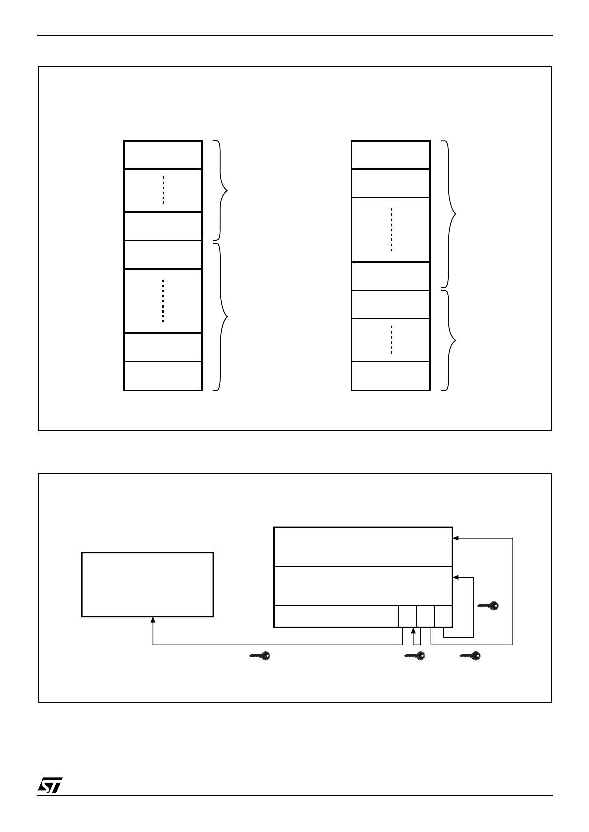
The device features an asymmetrical blocked ar-
chitecture. The M28R400C has an array of 15
blocks: 8 Parameter Blocks of 4 KWord and 7
Main Blocks of 32 KWord. M28R400CT has the
Parameter Blocks at the top of the memory address space while the M28R400CB locates the
Parameter Blocks starting from the bottom. The
memory maps are s hown in Figure 4, Block Addresses.
The M28R400C features an instant, individual
block locking scheme that allo ws any block to be
locked or unlocked with no latency, enabling instant code and data protection. All blocks have
three levels of protection. They can be locked and
locked-down individually preventing any accidental programming or erasure. There is an additional
hardware protection against program and block
erase. When V
PP
≤ V
PPLK
all blocks are p rotected
against program or block erase. All blocks are
locked at power-up.
Each block can be erased separately. Erase can
be suspended in order to perform either read or
program in any other block and then resumed.
Program can be suspended to read data in any
other block and then resumed. Each block can be
programmed and erased over 100,000 cycles.
The device includes a 128 b it Protection Regi ster
and a Security Block to increase the protection of
a system design. The Protection Register is divided into two 64 bit segments, the first one contains
a unique device number writte n by ST, while the
second one is one-time-programm able by the user. The user programmable segm ent can be permanently protected. The Security Block,
parameter block 0, can be perman ently protected
by the user. Figure 5, shows the Security Block
Memory Ma p.
Program and Erase c ommands are written to the
Command Interface of the memory. An on-chip
Program/Erase Controller takes care of the timings necessary for program and erase operations.
The end of a program or erase operation can be
detected and any error conditions identified. The
command set required to control the memory is
consistent with JEDEC standards.
The memory is offered in a TFBGA46 (0.75mm
pitch) package and is supplied with all the bits
erased (set to ’1’).
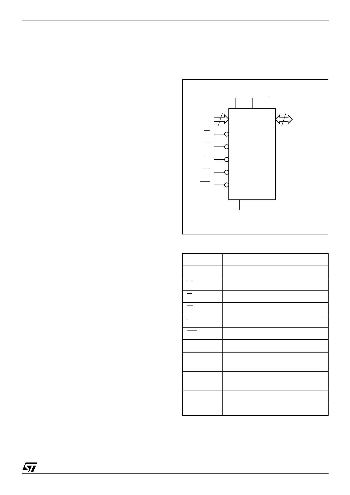
Figure 2. Logic Diagram
Table 1. Signal Names
A0-A17 Address Inputs
DQ0-DQ15 Data Input/Output
E
Chip Enable
G
Output Enable
W
Write Enable
RP
Reset
WP
Write Protect
V
DD
Core Power Supply
V
DDQ
Power Supply for
Input/Output
V
PP
Optional Supply Voltage for
Fast Program & Erase
V
SS
Ground
NC Not Connected Internally
AI04392
18
A0-A17
W
DQ0-DQ15
V
DD
M28R400CT
M28R400CB
E
V
SS
16
G
RP
WP
V
DDQVPP
Page 6
M28R400CT, M28R400CB
6/50
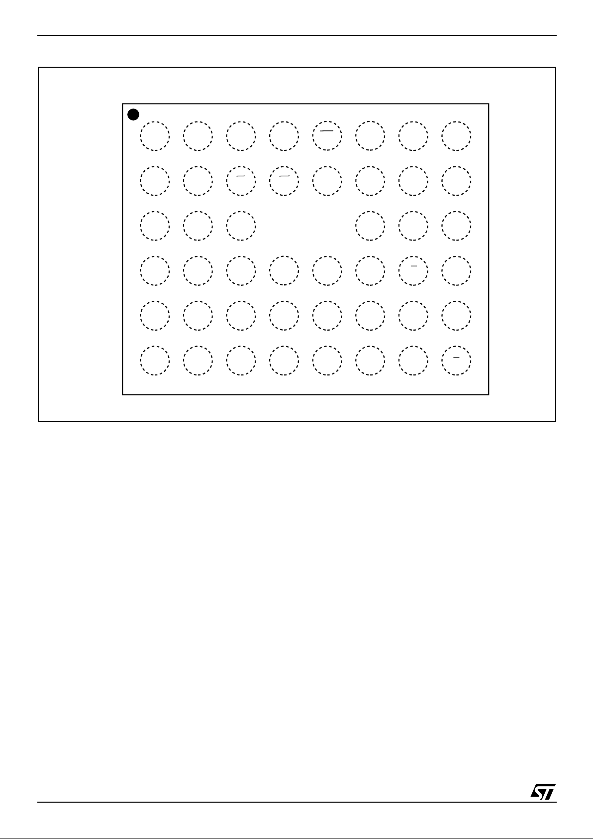
Figure 3. TFBGA Connections (Top view through package)
AI04142
C
B
A
87654321
E
D
F
A4
A7V
PP
A8A11
A13
A0EDQ8DQ5DQ14A16
V
SS
DQ0DQ9DQ3DQ6
DQ15
V
DDQ
DQ1DQ10V
DD
DQ7V
SS
DQ2
A2
A5A17WA10
A14
A1A3A6A9A12A15
RP NC
DQ4
DQ13
G
DQ12
DQ11
WP NC
Page 7
7/50
M28R400CT, M28R400CB
Figure 4. Block Addresses
Note: Also see Appe ndi x A, Tables 22 and 23 for a f ul l l isting of the B l ock Addresses.
Figure 5. Security Block Memory Map
AI04393
4 KWords
3FFFF
3F000
32 KWords
0FFFF
08000
32 KWords
07FFF
00000
M28R400CT
Top Boot Block Addresses
4 KWords
38FFF
38000
32 KWords
30000
37FFF
Total of 8
4 KWord Blocks
Total of 7
32 KWord Blocks
4 KWords
3FFFF
38000
32 KWords
32 KWords
00FFF
00000
M28R400CB
Bottom Boot Block Addresses
4 KWords
37FFF
0FFFF
32 KWords
30000
08000
Total of 7
32 KWord Blocks
Total of 8
4 KWord Blocks
07FFF
07000
AI03523
Parameter Block # 0
User Programmable OTP
Unique device number
Protection Register Lock 2 1 0
88h
85h
84h
81h
80h
Page 8

M28R400CT, M28R400CB
8/50
SIGNAL DESCRIPTIONS
See Figure 2 Logic Diagram and Table 1,Signal
Names, for a brief overview of the signals connected to this device.
Address Inputs (A0-A17). The Address Inputs
select the cell s in the memory arra y to access during Bus Read operations. During Bus Write operations they control the commands sent to the
Command Interface of the internal state machine.
Data Input/Output (DQ0-DQ15). The Data I/O
outputs the data stored at the selected address
during a Bus Read operation or inputs a command
or the data to be programmed durin g a Write Bus
operation.
Chip Enable (E
). The Chip Enable input acti-
vates the memory control logic, input buffers, decoders and sense amplifiers. When Chip Enable is
at V
IL
and Reset is at VIH the device is in active
mode. When Chi p E nable is at V
IH
the memory is
deselected, the outputs are high im pedance and
the power consumption is reduced to the stand-by
level.
Output Enable (G
). The Output Enable controls
data outputs during the Bus Read operation of the
memory.
Write Enable (W
). The Write Enable controls the
Bus Write operation of the memory’s Command
Interface. The data and address inputs are latched
on the rising edge of Chip Enable, E, or Write Enable, W
, whichever occurs first.
Write Protect (WP
). Write Protect is an input
that gives an additional hardware protection for
each block. When Write Protect is at V
IL
, the Loc kDown is enabled and the protection status of the
block cannot be changed. When Write Protect is at
V
IH
, the Lock-Down is disabled and the block can
be locked or unlocked. (refer to Table 6, Read Protection Register and Protection Register Lock).
Reset (RP
). The Reset input provides a hard-
ware reset of the mem ory. When Reset is at V
IL
,
the memory is in reset mode: the outputs are high
impedance and the current consumption is minimized. After Reset all blocks are in the Locked
state. When Reset is at V
IH
, the device is in normal
operation. Exiting reset mode the device enters
read array mode, but a negative transition of Chip
Enable or a c hange of the address is require d to
ensure valid data outputs.
V
DD
Supply Vol tag e (1 . 65 V to 2.2V) . V
DD
provides the power supply to the i nternal core of
the memory device. It is the main power supply for
all operations (Read, Program and Erase).
V
DDQ
Supply Voltage (1.65V to 2.2 V). V
DDQ
provides the power supply to the I/O pins and enables all Outputs to be powered independently
from V
DD
. V
DDQ
can be tied to VDD or can use a
separate supply.
V
PP
Program Supply Voltage. VPP is both a
control input and a power supply pin. The two
functions are selected by the voltage range applied to the pin. The Supply Voltage V
DD
and the
Program Supply Voltage V
PP
can be applied in
any order.
If V
PP
is kept in a low voltage range (0V to 3.6V)
V
PP
is seen as a control input. In this case a volt-
age lower than V
PPLK
gives protection against pro-
gram or block erase, while V
PP
> V
PP1
enables
these functions (see Table 14, DC Characteristics
for the relevant values). V
PP
is only sampled at the
beginning of a program or bloc k erase; a change
in its value after the operation has started does not
have any effect and program or erase operations
continue.
If V
PP
is in the range 11.4V to 12.6V it acts as a
power supply pin. In this condition V
PP
must be
stable until the Program/Erase al gorithm is completed (see Table 16 and 17).
V
SS
Ground. VSS is the ref erence for all voltage
measurements.
Note: Each device in a system should have
V
DD, VDDQ
and VPP decoupled with a 0.1µF ca-
pacitor close to the pin. See Figure 7, AC Measurement Load Circu it. The PCB trace widths
should be sufficient to carry the required V
PP
program and erase currents.
Page 9
9/50
M28R400CT, M28R400CB
BUS OPERATIONS
There are six standard bus operations that control
the device. These are B us Read, Bus Wri te, Output Disable, Standby, Automatic Standby and Reset. See Table 2, Bus Operations, for a summary.
Typically glitches of less than 5ns on Chip Enable
or Write Enable are ignored by the memory and do
not affect bus operations.
Read. Read Bus operations are used to ou tput
the contents of the Memory Array, the Electr onic
Signature, the Status Register and the Common
Flash Interface. Both Chip Enable and Output Enable must be at V
IL
in order to perform a read operation. The Chip Enable in put should b e used to
enable the device. Out put E nable s houl d be us ed
to gate data onto the output. The data read depends on the previous command written to the
memory (see Command Interface section). See
Figure 8, Read Mode AC Wa veforms, and Table
15, Read AC Characteristics, for details of when
the output becomes valid.
Read mode is the default state of the device when
exiting Reset or after power-up.
Write. Bus Write operations write Comm ands to
the memory or latch Input Data to be programmed.
A write operation is initiated when Chip Enable
and Write Enable are at V
IL
with Output Enable at
V
IH
. Commands, Input Data and Addresses are
latched on the rising edge of Write Enable or Chip
Enable, whichever occurs first.
See Figures 9 and 10, Write A C Wav eforms, and
Tables 16 and 17, Write AC Characteristics, for
details of the timing requirements.
Output Disable. The data outputs are high impedance when the Output Enable is at V
IH
.
Standby. S tandby disables m ost of the internal
circuitry allowing a substantial reduction of the current consumption. The memory is in stand-by
when Chip Enable is at V
IH
and the devic e is in
read mode. The power consumption is reduced to
the stand-by level and t he outputs are set to high
impedance, independently from the Output Enable
or Write Enable inputs. If Chip En able switches to
V
IH
during a program or erase operat ion, the de-
vice enters Standby mode when finished.
Automatic Standby. Automatic Standby pro-
vides a low power consumption state during Read
mode. Following a read operation, the device enters Automatic Standby after 150ns of bus inactivity even if Chip Enable is Low, V
IL
, and the supply
current is reduced to I
DD1
. The data Inputs/Outputs will still output data if a bus Read operation is
in progress.
Reset. During Reset mode when Output Enable
is Low, V
IL
, the memory is deselected and the outputs are high impedance. The memory is in Reset
mode when Reset is at V
IL
. The power consumption is reduced to the Standby level, independently
from the Chip Enable, Output Enable or Write Enable inputs. If Reset is pulled to V
SS
during a Program or Erase, this operation is aborted and the
memory content is no longer valid.
Table 2. Bus Operations
Note: X = VIL or VIH, V
PPH
= 12V ± 5%.
Operation E G W RP WP
V
PP
DQ0-DQ15
Bus Read
V
IL
V
IL
V
IH
V
IH
X Don’t Care Data Output
Bus Write
V
IL
V
IH
V
IL
V
IH
X
V
DD
or V
PPH
Data Input
Output Disable
V
IL
V
IH
V
IH
V
IH
X Don’t Care Hi-Z
Standby
V
IH
XX
V
IH
X Don’t Care Hi-Z
Reset X X X
V
IL
X Don’t Care Hi-Z
Page 10

M28R400CT, M28R400CB
10/50
COMMAND INTERFACE
All Bus Write operations to the memory are in terpreted by the Command Interface. Commands
consist of one or more sequential Bus Write operations. An internal Program/Erase Controller handles all timings and verifies the correct execution
of the Program and Erase commands. The Program/Erase Controller provides a S tatus Register
whose output may be read at any time during, to
monitor the progress of the operation, or t he Program/Erase states. See Appendix D, Table 30,
Write State Machine Current/Next, for a summary
of the Command Interface.
The Command Interface is reset to Read mode
when power is first applied, when exiting from Reset or whenever V
DD
is lower than V
LKO
. Command sequences must be followed exactly. Any
invalid combination of commands will reset the device to Read mode. Refer to Table 3, Commands,
in conjunction with the text descriptions below.
Read Memory Array Command
The Read command returns the memory to its
Read mode. One Bus Write cycle is required to issue the Read Memory Array command and return
the memory to Read mode . Subsequent read operations will read the addressed loc ation and output the data. When a device Reset occurs, the
memory defaults to Read mode.
Read Status Register Command
The Status Register indicates when a program or
erase operation is complete and the success or
failure of the operation itself. Issue a Read Status
Register command to rea d the Status Register’s
contents. Subsequent Bus Read operations read
the Status Register at any address , until another
command is issued. See Table 10, Status Register
Bits, for details on the definitions of the bits.
The Read Status Register command may be issued at any time, even during a Program/Erase
operation. Any Read attempt during a Program/
Erase operation will automatically outp ut the content of the Status Register.
Read Electronic Signature Command
The Read Electronic Signature command reads
the Manufacturer and Device Codes and the Block
Locking Status, or the Protection Register.
The Read Electronic Signature command consists
of one write cycle, a subsequent read will output
the Manufacturer Code, the Device Code, the
Block Lock and Lock-Down Status, or the Protection and Lock Register. See Tables 4, 5 and 6 for
the valid address.
Read CFI Query Command
The Read Query Command is used t o read data
from the Common Flash Interface (CFI ) Memory
Area, allowing programming equipment or appli-
cations to automatically match their interface to
the characteristics of the device. One Bus Write
cycle is required to issue the Read Query Command. Once the command is issued subsequent
Bus Read operations read from the Common
Flash Interface Memory Area. See Appendix B,
Common Flash Inte rface, Tables 2 4, 25, 26, 27,
28 and 29 for details on the information contained
in the Common Flash Interface memory area.
Block Erase Command
The Block Erase c ommand can be used to erase
a block. It sets all the bits within the selected block
to ’1’. A ll previous data in t he block is lost. If t he
block is protected then the Erase operation will
abort, the data in the block will not be changed and
the Status Register will output the error.
Two Bus Write cycles are required to issue the
command.
■ The first bus cycle sets up the Erase command.
■ The second latches the block address in the
internal state machine and starts the Program/
Erase Controller.
If the second bus cycle is not Write Erase Confirm
(D0h), Status Register bits b4 and b5 are s et and
the command aborts.
Erase aborts if Reset turns to V
IL
. As data integrity
cannot be guaranteed when the Erase operation is
aborted, the block must be erased again.
During Erase operations the memory will accept
the Read Status Register com mand and th e Program/Erase Suspend command, all other commands will be ignored. Typical Erase times are
given in Table 7, Program, Erase Times and Program/Erase Endurance Cycles.
See Appendix C, Figure 18, Block Erase Flowchart and Pseudo Code, for a suggested flowchart
for using the Block Erase command.
Chip Erase Command
The Chip Erase command can be used to erase
the entire chip. It sets all of the bits in unprotected
blocks of the memory to ’1’. All previous data is
lost. Two Bus Write operations are requ ired to issue the Chip Erase Command.
■ The first bus cycle sets up the Chip Erase
command.
■ The second confirms the Chip Erase command
and starts the Program/Erase Controller.
The command can be issued to any address. If
any blocks are protec ted then these are ignored
and all the other blocks are erased. If all of the
blocks are protected the Chip Erase op erat i on appears to start but wi ll terminate, leaving the data
unchanged. No error condition is gi ven when protected blocks are ignored.
Page 11

11/50
M28R400CT, M28R400CB
During the erase o peration th e memory w ill only
accept the Read Status Register command. All
other commands will be ignored, including the
Erase Suspend com mand. It is no t possible to issue any command to abort the operation.
Chip Erase commands should be limited to a maximum of 100 Program/Erase cycles. After 100 Program/Erase cycles the internal algorithm will still
operate properly but some degradation in performance may oc c ur.
Typical chip erase times are given in Table 7.
Program Command
The memory array can be programmed word-byword. Two bus write cycles are required to issue
the Program Command.
■ The first bus cycle sets up the Program
command.
■ The second latches the Address and the Data to
be written and starts the Program/Erase
Controller.
During Program operations the memory will accept the Read Status Register command and the
Program/Erase Suspend command. Typical Program times are given in Tab le 7, P rogram, Erase
Times and Program/Erase Endurance Cycles.
Programming aborts if Res et goes to V
IL
. As data
integrity cannot be guaranteed when the program
operation is aborted, the block containing the
memory location must be erased and reprogrammed.
See Appendix C, Figure 15, Program Flowchart
and Pseudo Code, for t he flowchart for using t he
Program command.
Double Word Program Command
This feature is offered to improve the programming
throughput, writing a page of two adjacent words
in parallel.The two words m ust differ only for the
address A0. Program m ing s hould not be attempted when V
PP
is not at V
PPH
. The command can be
executed if V
PP
is below V
PPH
but the result is not
guaranteed.
Three bus write cycles are necessary to issue the
Double Word Program command.
■ The first bus cycle sets up the Double Word
Program Command.
■ The second bus cycle latches the Address and
the Data of the first word to be written.
■ The third bus cycle latches the Address and the
Data of the second word to be written and starts
the Program/Erase Controller.
Read operations output the Status Register content after the programming has started. Programming aborts if Reset goe s to V
IL
. As data integrity
cannot be guaranteed when the program opera-
tion is aborted, the block containin g the memory
location must be erased and reprogrammed.
See Appendix C, Figure 16, Double Word Program Flowchart and Pseudo Code, for the flowchart for using the Double Word Program
command.
Clear Status Register Command
The Clear Status Register com m and can be used
to reset bits 1, 3, 4 and 5 in the Status Register to
‘0’. One bus write cycle is required to issue the
Clear Status Register command.
The bits in the Status Register do not automatically return to ‘0’ when a new Program or Erase command is issued. The error bits in the Status
Register should be cleared before attempting a
new Program or Erase command.
Program/Erase Suspend Command
The Program/Erase Suspend command is used to
pause a Program or Erase operation. One bus
write cycle is required to issue the Program/Erase
command and pause the Program/Erase controller.
During Program/Erase Suspend the Command Interface will accept the Program/Erase Resume,
Read Array, Read Status Register, Read Electronic Signature and Read CFI Query commands. Additionally, if the suspend operation was Erase then
the Program, Block Lock, Block Lock-Down or
Protection Program commands will also be accepted. The block being erased may be protected
by issuing the Block Protect, Block Lock or Protection Program commands. When the Program/
Erase Resume com mand is issued the operation
will complete. Only the blocks not being erased
may be read or programmed correctly.
During a Program/Erase Suspend, the device can
be placed in a pseudo-standby mode by taking
Chip Ena ble to V
IH
. Program/Erase is aborted if
Reset turns to V
IL
.
See Appendix C, Figure 17 , Program Suspend &
Resume Flowchart and Pseudo Code, and Figure
19, Erase Suspend & Resume Flowchart and
Pseudo Code for flowcharts for using the Program/
Erase Suspend command.
Program/Er ase Resu me Command
The Program/Erase Resume command can be
used to restart the Program/Erase Controller after
a Program/Erase Suspend operation has paused
it. One Bus Write cycle is required to issue the
command. Once the command is issued subsequent Bus Read operations read the Status Register.
See Appendix C, Figure 17 , Program Suspend &
Resume Flowchart and Pseudo Code, and Figure
19, Erase Suspend & Resume Flowchart and
Page 12

M28R400CT, M28R400CB
12/50
Pseudo Code for flowcharts for using the Program/
Erase Resume command.
Prot ection Register Program Command
The Protection Register Program command is
used to Program the 64 bit user One-Time-Programmable (OTP) segment of the Protection Register. The segment is programmed 16 bits at a
time. When shipped all bits in the segment are set
to ‘1’. The user can only program the bits to ‘0’.
Two write cycles are required to issue the Pro tec-
tion Register Program command.
■ The first bus cycle sets up the Protection
Register Program command.
■ The second latches the Address and the Data to
be written to the Protection Register and starts
the Program/Erase Controller.
Read operations output the Status Register content after the programming has started.
The segment can be protected by programming bit
1 of the Protection Lock Register. Bit 1 of the Protection Lock Register protects bit 2 of the Protection Lock Register. Programming bit 2 of the
Protection Lock Register will result in a permanent
protection of the Security Block (see Figure 5, Security Block Memory Map). Attempting to program
a previously protected Protection Register will result in a Status Register error. The protection of
the Protection Register a nd/or the Security Block
is not reversible.
The Protection Register Program cannot be suspended. See Appendix C, Figure 21, Protection
Register Program Flowchart and Pseudo Code,
for the flowchart for using th e Protection Regi ster
Program command.
Block Lock Command
The Block Lock command is used to lock a block
and prevent Program or Erase operations from
changing the data in it. All blocks are locked at
power-up or reset.
Two Bus Write cycles are required to issue the
Block Lock command.
■ The first bus cycle sets up the Block Lock
command.
■ The second Bus Write cycle latches the block
address.
The lock status c an be monitored for eac h block
using the Read Electronic Signature command.
Table. 9 shows the protection status after issuing
a Block Lock command.
The Block Lock bit s are volatile, once set they remain set until a hardware reset or power-down/
power-up. They are cleared by a Blocks Unlock
command. Refer to the section, Block Locking, for
a detailed explanation.
Block Unlock Command
The Blocks Unlock comm and is used to unlock a
block, allowing the block to be programmed or
erased. Two Bus Write cy cles are required to issue the Blocks Unlock command.
■ The first bus cycle sets up the Block Unlock
command.
■ The second Bus Write cycle latches the block
address.
The lock status c an be monitored for eac h block
using the Read Electronic Signature command.
Table. 9 shows the protection status after issuing
a Block Unlock command. Refer to the section,
Block Locking, for a detailed explanation.
Block Lock-Down Command
A locked block cannot be Programmed or Erased,
or have its protection status changed wh en WP
is
low, V
IL
. When WP is high, V
IH,
the Lock-Down
function is disabled and the locked bloc ks can be
individually unlocked by the Block Unlock command.
Two Bus Write cycles are required to issue the
Block Lock-Down command.
■ The first bus cycle sets up the Block Lock
command.
■ The second Bus Write cycle latches the block
address.
The lock status c an be monitored for eac h block
using the Read Electronic Signature command.
Locked-Down blocks revert to the locked (and not
locked-down) state when the device is reset on
power-down. Table. 9 shows the protection status
after issuing a Block Lock-Down co mmand. Refer
to the section, Block Locking, for a detailed explanation.
Page 13
13/50
M28R400CT, M28R400CB
Table 3. Commands
Note: 1. X = Don’t Care.
2. The signature addresses ar e l i st ed in Tables 4, 5 and 6.
3. Addr 1 and Addr 2 must be consecu tive Addres ses differ i ng only for A0.
Commands
No. of
Cycles
Bus Write Operations
1st Cycle 2nd Cycle 3nd Cycle
Bus
Op.
Addr Data
Bus
Op.
Addr Data
Bus
Op.
Addr Data
Read Memory Array 1+ Write X FFh
Read
Read
Addr
Data
Read Status Register 1+ Write X 70h
Read
X
Status
Register
Read Electronic Signature 1+ Write X 90h
Read
Signature
Addr
(2)
Signature
Read CFI Query 1+ Write 55h 98h Read CFI Addr Query
Block Erase 2 Write X 20h Write
Block
Addr
D0h
Chip Erase 2 Write X 80h Write X D0h
Program 2 Write X
40h or
10h
Write Addr
Data
Input
Double Word Pr ogram
(3)
3 Write X 30h Write Addr 1
Data
Input
Write Addr 2
Data
Input
Clear Status Register 1 Write X 50h
Program/E rase Suspend 1 W rite X B 0h
Program/Erase Resume 1 Wr ite X D0h
Block Lock 2 Write X 60h Write
Block
Address
01h
Block Unlock 2 Write X 60h Write
Block
Address
D0h
Block Lock-Down 2 Write X 60h Write
Block
Address
2Fh
Protection Register
Program
2 Write X C0h Write
Address
Data
Input
Page 14
M28R400CT, M28R400CB
14/50
Table 4. Read Electronic Signature
Note: RP = VIH.
Table 5. Read Block Lock Signature
Note: 1. A Lo ck ed-Down Block can be locked "DQ0 = 1" or unlock ed "DQ0 = 0"; see Block Lock i ng section.
Table 6. Read Protection Register and Lock Register
Code Device E G W A0 A1 A2-A7 A8-A17 D Q0-DQ7 DQ8-DQ15
Manufacture.
Code
V
IL
V
IL
V
IH
V
IL
V
IL
0 Don’t Care 20h 00h
Device Code
M28R400CT
V
IL
V
IL
V
IH
V
IH
V
IL
0 Don’t Care 2Ah 88h
M28R400CB
V
IL
V
IL
V
IH
V
IH
V
IL
0 Don’t Care 2Bh 88h
Block Status E
G W A0 A1 A2-A7 A8-A11 A12-A17 DQ0 DQ1 DQ2-DQ15
Locked Block
V
IL
V
IL
V
IHVIL
V
IH
0 Don’t Care Block Address 1 0 00h
Unlocked Block
V
IL
V
IL
V
IHVIL
V
IH
0 Don’t Care Block Address 0 0 00h
Locked-Down
Block
V
IL
V
IL
V
IHVIL
V
IH
0 Don’t Care Block Address
X
(1)
1 00h
Word E
G W A0-A7 A8-A17 DQ0 DQ1 DQ2 DQ3-DQ7 DQ8-DQ15
Lock
V
IL
VILV
IH
80h Don’t Care 0
OTP Prot.
data
Security
prot. data
00h 00h
Unique ID 0
V
IL
VILV
IH
81h Don’t Care ID data ID data ID data ID data ID data
Unique ID 1
V
IL
VILV
IH
82h Don’t Care ID data ID data ID data ID data ID data
Unique ID 2
V
IL
VILV
IH
83h Don’t Care ID data ID data ID data ID data ID data
Unique ID 3
V
IL
VILV
IH
84h Don’t Care ID data ID data ID data ID data ID data
OTP 0
V
IL
VILV
IH
85h Don’t Care OTP data OTP data OTP data OTP data OTP data
OTP 1
V
IL
VILV
IH
86h Don’t Care OTP data OTP data OTP data OTP data OTP data
OTP 2
V
IL
VILV
IH
87h Don’t Care OTP data OTP data OTP data OTP data OTP data
OTP 3
V
IL
VILV
IH
88h Don’t Care OTP data OTP data OTP data OTP data OTP data
Page 15
15/50
M28R400CT, M28R400CB
Table 7. Program, Erase Times and Program/Erase Endura nce Cycles
Parameter Test Conditions
M28R400C
Unit
Min Typ Max
Word Program
V
PP
= V
DD
10 200 µs
Double Word Program
V
PP
= 12V ±5%
10 200 µs
Main Block Program
V
PP
= 12V ±5%
0.16 5 s
V
PP
= V
DD
0.32 5 s
Parameter Block Program
V
PP
= 12V ±5%
0.02 4 s
V
PP
= V
DD
0.04 4 s
Main Block Erase
V
PP
= 12V ±5%
110 s
V
PP
= V
DD
110 s
Chip Erase (preprogrammed)
V
PP
= 12V ±5%
210 s
V
PP
= V
DD
210 s
Chip Program
V
PP
= 12V ±5%
1.25 s
V
PP
= V
DD
25 s
Parameter Block Erase
V
PP
= 12V ±5%
0.8 10 s
V
PP
= V
DD
0.8 10 s
Program/Erase Cycles (per Block) 100,000 cycles
Page 16

M28R400CT, M28R400CB
16/50
BLOCK LOCKING
The M28R400C features an instant, individual
block locking scheme that allo ws any block to be
locked or unlocked with no latency. This locking
scheme has three levels of protection.
■ Lock/Unlock - this first level allows software-
only control of block locking.
■ Lock-Down - this second level requires
hardware interaction before locking can be
changed.
■ V
PP
≤ V
PPLK
- the third level offers a hardware
protection against program and block erase on
all blocks.
The lock status of each block can be set to
Locked, Unlocked, and Lock- Down. Table 9, defines all of the possible protection states (WP
,
DQ1, DQ0), and Appendi x C, Figure 20, shows a
flowchart for the locking operations.
Reading a Block’s Lock Status
The lock status of every block can be read in the
Read Electronic Signature mode of the device. To
enter this mode write 90h to the device. Subsequent reads at the address specified in Table 5,
will output the lock statu s of that block. The lock
status is represented by DQ0 and DQ1. DQ0 indicates the Block Lock/Unlock status an d is set by
the Lock command and cleared by the Unlock
command. It is also automatically set when en tering Lock-Down. DQ1 indicates the Lock-Down status and is set by the Lock-Down command. It
cannot be cleared by software, only by a hardware
reset or power-down.
The following sections explain the operation of the
locking system.
Locked State
The default status of all blocks on power-up or after a hardware reset is L ocked (states (0,0,1) or
(1,0,1)). Locked blocks are fully protected from
any program or erase. Any program or erase operations attempted on a locked block will return an
error in the Status Register. The Status of a
Locked block can be changed to Unlocked or
Lock-Down using the appropriate software commands. An Unlocked block can be Locked by issuing the Lock command.
Unlocked State
Unlocked blocks (states (0,0,0), (1,0,0) (1,1,0)),
can be programmed or erased. All unlocked
blocks return to the Locked state a fter a hardware
reset or when the device is powered-down. The
status of an unlocked block can be changed to
Locked or Locked-Down using the appropriate
software commands. A locked block can be unlocked by issuing the Unlock command.
Lock-Down State
Blocks that are Locked-Down (state (0,1,x))are
protected from program and erase operat ions (as
for Locked blocks) but their lock status cannot be
changed using software commands alone. A
Locked or Unlocked block can be Locked-Down by
issuing the Lock-Down command. Locked-Down
blocks revert to the Locked state when the device
is reset or powered-down.
The Lock-Down function is depen dent on t he WP
input pin. When WP=0 (VIL), the blocks in the
Lock-Down state (0,1,x) are protected from program, erase and protection status changes. When
WP
=1 (VIH) the Lock-Down function is disabled
(1,1,1) and Locked-Down blocks can be individually unlocked to the (1,1,0) state by issuing the
software command, where they can be erased and
programmed. These blocks can then be relocked
(1,1,1) and unlocked (1,1,0) as desired while WP
remains high. When WP is low , blocks that were
previously Locked-Down return to the Lock-Down
state (0,1,x) regardless of any changes made
while WP
was high. Device reset or power-down
resets all blocks , including those in Lock-Down, to
the Locked state.
Locking Operations During Erase Suspend
Changes to block lock status can be performed
during an erase suspend by using the standard
locking command sequences to unlock, lock or
lock-down a block. This is useful in the case when
another block needs to be updated while an erase
operation is in progress.
To change block locking during an erase operation, first write the Erase Suspend command, then
check the status register until it indicates that the
erase operation has been suspended. Nex t write
the desired Lock com mand sequence to a block
and the protection status will be changed. After
completing any desired lock, read, or program operations, resume the erase operation with the
Erase Resume command.
If a block is locked or locked-down during an erase
suspend of the same block, the locking status bits
will be changed immediately , but when the eras e
is resumed, the erase operation will complete.
Locking operations cannot be perform ed during a
program suspend. Refer to Appendix D, Command Interface and Program/Erase Controller
State, for detailed information on which commands are valid during erase suspend.
Page 17

17/50
M28R400CT, M28R400CB
Table 8. Block Lock Status
Table 9. Protection Status
Note: 1. The prote ct i on status i s defined by the write prot ect pin and by DQ 1 (‘1’ for a l ocked-down block) and DQ0 (‘1’ for a locked block)
as read in the Read Electr oni c Signature command with A1 = V
IH
and A0 = VIL.
2. All blocks are locke d at power-up, so the default configuration i s 001 or 101 according to WP
status.
3. A WP
transition to VIH on a locked block will res t or e the previous DQ0 value, giving a 111 or 110.
Item Address Data
Block Lock Configuration
xx002
LOCK
Block is Unlocked DQ0=0
Block is Locked DQ0=1
Block is Locked-Down DQ1=1
Current
Protection Status
(1)
(WP, DQ1, DQ0)
Next Protection Status
(1)
(WP, DQ1, DQ0)
Current State
Program/Erase
Allowed
After
Block Lock
Command
After
Block Unlock
Command
After Block
Lock-Down
Command
After
WP
transition
1,0,0 yes 1,0,1 1,0,0 1,1,1 0,0,0
1,0,1
(2)
no 1,0,1 1,0,0 1,1,1 0,0,1
1,1,0 yes 1,1,1 1,1,0 1,1,1 0,1,1
1,1,1 no 1,1,1 1,1,0 1,1,1 0,1,1
0,0,0 yes 0,0,1 0,0,0 0,1,1 1,0,0
0,0,1
(2)
no 0,0,1 0,0,0 0,1,1 1,0,1
0,1,1 no 0,1,1 0,1,1 0,1,1
1,1,1 or 1,1,0
(3)
Page 18

M28R400CT, M28R400CB
18/50
STATUS REGISTER
The Status Register provides information on the
current or previous Program or Erase operation.
The various bits convey information and errors on
the operation. To read the Status register the
Read Status Register command can be issued, refer to Read Status Register Command section. To
output the contents, the Status Register is latched
on the falling edge of the Chip Enable or Output
Enable signals, and can be read until Chip Enable
or Output Enable returns to V
IH
. Either Chip Enable or Output Enable must be toggled t o update
the latched data.
Bus Read operations from any address always
read the Status Register during Program and
Erase operations.
The bits in the Status Register are summari zed in
Table 10, Status Register Bits. Refer to Tabl e 10
in conjunction with the following text descriptions.
Program/Erase Controller Status (Bit 7). The P rogra m/Erase Controller Status bit indicates whether
the Program/Erase Controller is active or inactive.
When the Program/Erase Controller S tatus bit is
Low (set to ‘0’), the Program/Erase Controller is
active; when the bit is High (set to ‘1’), the Program/Erase Controller is inactive, and the device
is ready to process a new command.
The Program/Erase Controller Status is Low immediately after a Program/Erase Suspend command is issued until the Program/Erase Controller
pauses. After the Program/Erase Controller pauses the bit is High .
During Program, Erase, o perations the Program/
Erase Controller Status bit can be polled to find the
end of the operation. Other bits in the Status Register should not be tested until the Program/Erase
Controller completes the operation and the bit is
High.
After the Program/Erase Controller completes its
operation the Erase Status, Prog ram Status, V
PP
Status and Block Lock Status bits should be tested
for errors.
Erase Suspend Status (Bit 6). The Erase Suspend Status bit indicates that an Erase operation
has been suspended or is going to be suspended.
When the Erase Suspend Status bit is High (set to
‘1’), a Program/Erase Suspend command has
been issued and the memory is waiting for a Program/Erase Resume command.
The Erase Suspend Status should only be considered valid when the Program/Erase Controller Status bit is High (Program/Erase Controller inactive).
Bit 7 is set within 30µs of the Program/Erase Suspend command being issued therefore the memory may still complete the operation rather than
entering the Suspend mode.
When a Program/Erase Re sume command is issued the Erase Suspend Status bit returns Low.
Erase Status (Bit 5). The Erase Status bit can be
used to identify if the me mory has failed to verify
that the block has erased correctly. When the
Erase Status bit is High (set to ‘1’), the Program/
Erase Controller has applied the m aximum number of pulses to the block and still failed to verify
that the block has erased correctly. The Erase Status bit should be read once the Program/Erase
Controller Status bit is High (Program/Erase Controller inactive).
Once set High, the Erase Status bit can only be reset Low by a Clear Status Register command or a
hardware reset. If set High it should be reset before a new Program or Erase command is issued,
otherwise the new command will appear to fail.
Program Status (Bit 4). The Program Status bit
is used to identify a Program failure. When the
Program Status bit is High (set to ‘1’), the Program/Erase Controller has applied the maximum
number of pulses to the byte and still failed to verify that it has programmed correctly. The Program
Status bit should be read once the Program/Erase
Controller Status bit is High (Program/Erase Controller inactive).
Once set High, the Program Status bit can only be
reset Low by a Clear Status Register command or
a hardware reset. If set High it should be reset before a new command is issued, otherwise the new
command will appear to fail.
V
PP
Status (Bit 3). The VPP Status bit can be
used to identify an invali d voltage on the V
PP
pin
during Program and Erase operations. The V
PP
pin is only sampled at the beginning of a Program
or Erase operation. Indeterminate results can occur if V
PP
becomes invalid during an operation.
When the V
PP
Status bit is Low (set to ‘0’), the volt-
age on the V
PP
pin was sampled at a valid voltage;
when the V
PP
Status bit is High (set to ‘1’), the V
PP
pin has a voltage that is below the VPP Lockout
Voltage, V
PPLK
, program and block erase opera-
tions cannot be performed.
Once set High, the V
PP
Status bit can only be reset
Low by a Clear Status Register command or a
hardware reset. If set High it should be reset before a new Program or Erase command is issued,
otherwise the new command will appear to fail.
Program Suspend Status (Bit 2). The Program
Suspend Status bit indicates that a Program operation has been suspended. When the Program
Suspend Status bit is High (set to ‘1’), a Program/
Erase Suspend command has been issued and
the memory is waiting for a Program/Erase Resume command. The Program Suspend Status
should only be considered valid when the Pro-
Page 19

19/50
M28R400CT, M28R400CB
gram/Erase Controller Status bit is High (Program/
Erase Controller inactive). Bit 2 is set wi thin 5µs of
the Program/Erase Suspend command being issued therefore the memory may s till complete the
operation rather than entering the Suspend mode.
When a Program/Erase Re sume command is issued the Program Suspend Status bit returns Low.
Block Protection Status (Bit 1). The Block Protection Status bit can be used to identify if a Program or Erase operation has tried to modify the
contents of a locked block.
When the Block Protection Status bit is High (set
to ‘1’), a Program or Erase operation has been attempted on a locked block.
Once set High, the Block Protection Status bit can
only be reset Low by a Clear Status Register command or a hardware reset. If set High it should be
reset before a new command is issued, otherwise
the new command will appear to fail.
Reserved (Bit 0). Bit 0 of the Status Register is
reserved. Its value must be masked.
Note: Refer to Appendix C, Flowcharts and
Pseudo Codes, for using the Status Register.
Table 10. Status Register Bits
Note: Logic level ’1’ is High, ’0’ is Low.
Bit Name Logic Level Definition
7 P/E.C. Status
’1’ Ready
’0’ Busy
6 Erase Suspend Status
’1’ Suspended
’0’ In progress or Completed
5 Erase Status
’1’ Erase Error
’0’ Erase Success
4 Program Status
’1’ Program Error
’0’ Program Succ ess
3
V
PP
Status
’1’
V
PP
Invalid, Abort
’0’
V
PP
OK
2 Program Suspend Status
’1’ Suspended
’0’ In Progress or Completed
1 Block Protection Status
’1’ Program/Erase on protected Block, Abort
’0’ No operation to protected blocks
0 Reserved
Page 20

M28R400CT, M28R400CB
20/50
MAXIMUM RATI N G
Stressing the de vice above the rating l isted in t he
Absolute Maximum Ratings t able may cause permanent damage to the device. T hese are stress
ratings only and operation of the device at t hese or
any other conditions ab ove thos e indicated i n the
Operating sections of this spec ification is not im-
plied. Exposure to Absolute Maximum Rating conditions for extended periods may affect device
reliability. Refer also to the STMicroelectronics
SURE Program and other relevant quality documents.
Table 11. Absolute Maximum Ratings
Note: 1. Depends on range.
Symbol Parameter
Value
Unit
Min Max
T
A
Ambient Operating Temperature
(1)
– 40 85 °C
T
BIAS
Temperature Under Bias – 40 125 °C
T
STG
Storage Temperat ure – 5 5 155 °C
V
IO
Input or Output Voltage – 0.5
V
DDQ
+ 0.5
V
V
DD
, V
DDQ
Supply Voltage – 0.5 2.7 V
V
PP
Program Voltage – 0.5 13 V
t
VPPH
Time for VPP at V
PPH
100 hours
Page 21

21/50
M28R400CT, M28R400CB
DC AND AC PARAMETERS
This section summarizes t he operating and measurement conditions, and the DC and AC characteristics of the device. The parameters i n the DC
and AC characteristics Tables that follow, are derived from tests performed under the Measure-
ment Conditions summarized in Table 12,
Operating and AC Meas urement Conditions. Designers should check that the operating conditions
in their circuit match the measurement conditions
when relying on the quoted parameters.
Table 12. Operating and AC Measurement Conditions
Figure 6. AC Measurement I/O Waveform Figure 7. AC Measurement Load Circuit
Table 13. Capacitance
Note: Sam pled only, not 100% tested.
Parameter
M28R400CT, M28R400CB
Units90 120
MinMaxMinMax
V
DD
Supply Voltage
1.7 2.0 1.65 2.2 V
V
DDQ
Supply Voltage (V
DDQ
≤ V
DD
)
1.7 2.0 1.65 2.2 V
Ambient Operating Tem peratur e – 40 85 – 40 85 °C
Load Capacitance (C
L
)
30 30 pF
Input Rise and Fall Times 10 10 ns
Input Pulse Voltages
0 to V
DDQ
0 to V
DDQ
V
Input and Output Timing Ref. Voltages
V
DDQ
/2 V
DDQ
/2
V
AI00610
V
DDQ
0V
V
DDQ
/2
AI00609C
V
DDQ
CL
CL includes JIG capacitance
25kΩ
DEVICE
UNDER
TEST
0.1µF
V
DD
0.1µF
V
DDQ
25kΩ
Symbol Parameter Test Condition Min Max Unit
C
IN
Input Capacitance
V
IN
= 0V
6pF
C
OUT
Output Capacitance
V
OUT
= 0V
12 pF
Page 22

M28R400CT, M28R400CB
22/50
Table 14. DC Characteristics
Symbol Parameter Test Condition Min Typ Max Unit
I
LI
Input Leakage Current
0V≤ V
IN
≤ V
DDQ
±1 µA
I
LO
Output Leakage Current
0V
≤
V
OUT
≤V
DDQ
±10 µA
I
DD
Supply Current (Read)
E
= VSS, G = VIH, f = 5MHz
10 20 mA
I
DD1
Supply Current (Stand-by or
Automatic Stand-by)
E
= V
DDQ
± 0.2V,
RP
= V
DDQ
± 0.2V
15 50 µA
I
DD2
Supply Current
(Reset)
RP
= VSS ± 0.2V
15 50 µA
I
DD3
Supply Current (Program)
Program in progress
V
PP
= 12V ± 5%
10 20 mA
Program in progress
V
PP
= V
DD
10 20 mA
I
DD4
Supply Current (Erase)
Erase in progress
V
PP
= 12V ± 5%
520mA
Erase in progress
V
PP
= V
DD
520mA
I
DD5
Supply Current
(Program/Erase Suspend)
E
= V
DDQ
± 0.2V,
Erase suspended
50 µA
I
PP
Program Current
(Read or Stand-by)
V
PP
> V
DD
400 µA
I
PP1
Program Current
(Read or Stand-by)
V
PP
≤ V
DD
5µA
I
PP2
Program Current (Reset)
RP
= VSS ± 0.2V
5µA
I
PP3
Program Current (Program)
Program in progress
V
PP
= 12V ± 5%
10 mA
Program in progress
V
PP
= V
DD
5µA
I
PP4
Program Current (Erase)
Erase in progress
V
PP
= 12V ± 5%
10 mA
Erase in progress
V
PP
= V
DD
5µA
V
IL
Input Low Voltage –0.5 0.4 V
V
IH
Input High Voltage
V
DDQ
–0.4 V
DDQ
+0.4
V
V
OL
Output Low Voltage
I
OL
= 100µA, VDD = V
DD
min,
V
DDQ
= V
DDQ
min
0.1 V
V
OH
Output High Voltage
I
OH
= –100µA, VDD = V
DD
min,
V
DDQ
= V
DDQ
min
V
DDQ
–0.1
V
V
PP1
Program Voltage (Program or
Erase operations)
1.65 2.2 V
V
PPH
Program Voltage
(Program or Erase
operations)
11.4 12.6 V
V
PPLK
Program Voltage
(Program and Erase lock-out)
1V
V
LKO
VDD Supply Voltage (Program
and Erase lock-out)
2V
Page 23

23/50
M28R400CT, M28R400CB
Figure 8. Read AC Waveforms
Table 15. Read AC Characteristics
Note: 1. Sampled only, not 100% tested.
2. G
may be delayed by up to t
ELQV
- t
GLQV
after the fa l ling edge of E without increasing t
ELQV
.
Symbol Alt Parameter
M28R400C
Unit
90 120
t
AVAV
t
RC
Address Valid to Next Address Valid Min 90 120 ns
t
AVQV
t
ACC
Address Valid to Output Valid Max 90 120 ns
t
AXQX
(1)
t
OH
Address Transition to Output Transition Min 0 0 ns
t
EHQX
(1)
t
OH
Chip Enable High to Output Transition Min 0 0 ns
t
EHQZ
(1)
t
HZ
Chip Enable High to Output Hi-Z Max 25 30 ns
t
ELQV
(2)
t
CE
Chip Enable Low to Output Valid Max 90 120 ns
t
ELQX
(1)
t
LZ
Chip Enable Low to Output Transition Min 0 0 ns
t
GHQX
(1)
t
OH
Output Enable High to Output Transition Min 0 0 ns
t
GHQZ
(1)
t
DF
Output Enable High to Output Hi-Z Max 25 30 ns
t
GLQV
(2)
t
OE
Output Enable Low to Output Valid Max 30 35 ns
t
GLQX
(1)
t
OLZ
Output Enable Low to Output Transition Min 0 0 ns
DQ0-DQ15
AI04144b
VALID
A0-A17
E
tAXQX
tAVAV
VALID
tAVQV
tELQV
tELQX
tGLQV
tGLQX
ADDR. VALID
CHIP ENABLE
OUTPUTS
ENABLED
DATA VALID STANDBY
G
tGHQX
tGHQZ
tEHQX
tEHQZ
Page 24

M28R400CT, M28R400CB
24/50
Figure 9. Write AC Waveforms, Write Enable Con trolled
E
G
W
DQ0-DQ15 COMMAND CMD or DATA
STATUS REGISTER
V
PP
VALIDA0-A17
tAVAV
tQVVPL
tAVWH
tWHAX
PROGRAM OR ERASE
tELWL tWHEH
tWHDX
tDVWH
tWLWH
tWHWL
tVPHWH
SET-UP COMMAND CONFIRM COMMAND
OR DATA INPUT
STATUS REGISTER
READ
1st POLLING
tELQV
AI04145b
tWPHWH
WP
tWHGL
tQVWPL
tWHEL
Page 25

25/50
M28R400CT, M28R400CB
Table 16. Write AC Characteristics, Write Enable Controlled
Note: 1. Sampled only, not 100% tested.
2. Applicable if V
PP
is seen as a logic input (VPP < 2.2V ).
Symbol Alt Parameter
M28R400C
Unit
90 120
t
AVAV
t
WC
Write Cycle Time Min 90 120 ns
t
AVWH
t
AS
Address Valid to Write Enable High Min 50 50 ns
t
DVWH
t
DS
Data Valid to Write Enable High Min 50 50 ns
t
ELWL
t
CS
Chip Enable Low to Write Enable Low Min 0 0 ns
t
ELQV
Chip Enable Low to Output Valid Min 90 120 ns
t
QVVPL
(1,2)
Output Valid to VPP Low
Min 0 0 ns
t
QVWPL
Output Valid to Write Protect Low Min 0 0 ns
t
VPHWH
(1)
t
VPS
VPP High to Write Enable High
Min 200 200 ns
t
WHAX
t
AH
Write Enable High to Address Transition Min 0 0 ns
t
WHDX
t
DH
Write Enable High to Data Transition Min 0 0 ns
t
WHEH
t
CH
Write Enable High to Chip Enable High Min 0 0 ns
t
WHEL
Write Enable High to Chip Enable Low Min 30 30 ns
t
WHGL
Write Enable High to Output Enable Low Min 30 30 ns
t
WHWL
t
WPH
Write Enable High to Write Enable Low Min 30 30 ns
t
WLWH
t
WP
Write Enable Low to Write Enable High Min 50 50 ns
t
WPHWH
Write Protect High to Write Enable High Min 50 50 ns
Page 26

M28R400CT, M28R400CB
26/50
Figure 10. Write AC Waveforms, Chip Enable Controlled
E
G
DQ0-DQ15 COMMAND
CMD or DATA STATUS REGISTER
V
PP
VALIDA0-A17
tAVAV
tQVVPL
tAVEH
tEHAX
PROGRAM OR ERASE
tWLEL tEHWH
tEHDX
tDVEH
tELEH
tEHEL
tVPHEH
POWER-UP AND
SET-UP COMMAND
CONFIRM COMMAND
OR DATA INPUT
STATUS REGISTER
READ
1st POLLING
tELQV
AI04146b
W
tWPHEH
WP
tEHGL
tQVWPL
Page 27

27/50
M28R400CT, M28R400CB
Table 17. Write AC Characteristics, Chip Enable Controlled
Note: 1. Sampled only, not 100% tested.
2. Applicable if V
PP
is seen as a logic input (VPP < 2.2V ).
Symbol Alt Parameter
M28R400C
Unit
90 120
t
AVAV
t
WC
Write Cycle Time Min 90 120 ns
t
AVEH
t
AS
Address Valid to Chip Enable High Min 50 50 ns
t
DVEH
t
DS
Data Valid to Chip Enable High Min 50 50 ns
t
EHAX
t
AH
Chip Enable High to Address Transition Min 0 0 ns
t
EHDX
t
DH
Chip Enable High to Data Transition Min 0 0 ns
t
EHEL
t
CPH
Chip Enable High to Chip Enable Low Min 30 30 ns
t
EHGL
Chip Enable High to Output Enable Low Min 30 30 ns
t
EHWH
t
WH
Chip Enable High to Write Enable High Min 0 0 ns
t
ELEH
t
CP
Chip Enable Low to Chip Enable High Min 50 50 ns
t
ELQV
Chip Enable Low to Output Valid Min 90 120 ns
t
QVVPL
(1,2)
Output Valid to VPP Low
Min 0 0 ns
t
QVWPL
Data Valid to Write Protect Low Min 0 0 ns
t
VPHEH
(1)
t
VPS
VPP High to Chip Enable High
Min 200 200 ns
t
WLEL
t
CS
Write Enable Low to Chip Enable Low Min 0 0 ns
t
WPHEH
Write Protect High to Chip Enable High Min 50 50 ns
Page 28

M28R400CT, M28R400CB
28/50
Figure 11. Power-Up and Reset AC Waveforms
Table 18. Power-Up and Reset AC Characteristics
Note: 1. T he device Reset is possible but no t guaranteed if t
PLPH
< 100ns.
2. Sampled only, not 100% tested.
3. It is important to ass ert RP
in order to al l ow proper CP U i ni tializat i on during power up or reset.
Symbol Parameter Test Condition
M28R400C
Unit
90 120
t
PHWL
t
PHEL
t
PHGL
Reset High to Write Enable Low, Chip Enable Low,
Output Enable Low
During
Program and
Erase
Min 50 50 µs
others Min 30 30 ns
t
PLPH
(1,2)
Reset Low to Reset High Min 100 100 ns
t
VDHPH
(3)
Supply Voltages High to Reset High Min 50 50 µs
AI03537b
W,
RP
tPHWL
tPHEL
tPHGL
E, G
VDD, VDDQ
tVDHPH
tPHWL
tPHEL
tPHGL
tPLPH
Power-Up Reset
Page 29

29/50
M28R400CT, M28R400CB
PACKAGE MECHANICAL
Figure 12. TFBGA46 6.39x6.37mm - 8x6 ball array, 0.75 mm pitch, Bottom View Package Outline
Note: Drawing is not to scale.
Table 19. TFBGA46 6.39x6.37mm - 8x6 ball array, 0.75 mm pitch, Package Mecha nical Data
Symbol
millimeters inches
Typ Min Max Typ Min Max
A 1.200 0.0472
A1 0.200 0.0079
A2 1.000 0.0394
b 0.400 0.350 0.450 0.0157 0.0138 0.0177
D 6.390 6.290 6.490 0.2516 0.2476 0.2555
D1 5.250 – – 0.2067 – –
ddd 0.100 0.0039
E 6.370 6.270 6.470 0.25 08 0.2469 0.2547
e 0.750 – – 0.0295 – –
E1 3.750 – – 0.14 76 – –
FD 0.570 – – 0.02 24 – –
FE 1.310 – – 0.0516 – –
SD 0.375 – – 0.0148 – –
SE 0.375 – – 0.01 48 – –
E1E
D1
D
b
A2
A1
A
BGA-Z13
ddd
e
e
FD
FE
SD
SE
BALL "A1"
Page 30

M28R400CT, M28R400CB
30/50
Figure 13. TFBGA46 Daisy Chain - Package Connections (Top view through packa ge)
Figure 14. TFBGA46 Daisy Chain - PCB Connections proposal (Top view through package)
AI03860
C
B
A
87654321
E
D
F
AI03861
C
B
A
87654321
E
D
F
START
POINT
END
POINT
Page 31

31/50
M28R400CT, M28R400CB
PART NUMBERING
Table 20. Ordering Information Scheme
Table 21. Daisy Chain Ordering Scheme
Note:Devices are shipped from the factory with the memory content bits erased to ’1’. For a list of available
options (Speed, Package, etc.) or for further information on any aspect of this device, please contact
the ST Sales Office nearest to you.
Example: M28R400CT 120 ZB 6 T
Device Type
M28
Operating Voltage
R = V
DD
= 1.65V to 2.2V; V
DDQ
= 1.65V or 2.2V
Device Function
400C = 4 Mbit (256Kb x16), Boot Block
Array Matrix
T = Top Boot
B = Bottom Boot
Speed
90 = 90ns
120 = 120ns
Package
ZB = TFBGA46: 0.75mm pitch
Temperature Range
1 = 0 to 70 °C
6 = –40 to 85 °C
Option
T = Tape & Reel Packing
Example: M28R400C -ZB T
Device Type
M28R400C
Daisy Chain
-ZB = TFBGA46: 0.75 mm pitch
Option
T = Tape & Reel Packing
Page 32

M28R400CT, M28R400CB
32/50
APPENDIX A. BLOCK ADDRESS T ABLES
Table 22. Top Boot Block Addresses,
M28R400CT
Table 23. Bottom Boot Block Addresses,
M28R400CB
#
Size
(KWord)
Address Range
0 4 3F000-3FFFF
1 4 3E000-3EFFF
2 4 3D000-3DFFF
3 4 3C000-3CFFF
4 4 3B000-3BFFF
5 4 3A000-3AFFF
6 4 39000-39FFF
7 4 38000-38FFF
8 32 30000-37FFF
9 32 28000-2FFFF
10 32 20000-27FFF
11 32 18000-1FFFF
12 32 10000-17FFF
13 32 08000-0FFFF
14 32 00000-07FFF
#
Size
(KWord)
Address Range
14 32 38000-3FFFF
13 32 30000-37FFF
12 32 28000-2FFFF
11 32 20000-27FFF
10 32 18000-1FFFF
9 32 10000-17FFF
8 32 08000-0FFFF
7 4 07000-07FFF
6 4 06000-06FFF
5 4 05000-05FFF
4 4 04000-04FFF
3 4 03000-03FFF
2 4 02000-02FFF
1 4 01000-01FFF
0 4 00000-00FFF
Page 33

33/50
M28R400CT, M28R400CB
APPENDIX B. COMMON FLASH INTERFACE (CFI)
The Common Flash Interface is a JEDEC approved, standardized data structure that can be
read from the Flash memory device. It allows a
system software to query the de vic e to determine
various electrical and timing parameters, density
information and function s supported by t he memory. The system can interface easily with the device, enabling the software to upgrade itself when
necessary.
When the CFI Query Co mmand (RCFI) is issued
the device enters CFI Que ry mode and the data
structure is read from the memory. Tables 24 , 25,
26, 27, 28 and 29 show the addresses used to retrieve the data.
The CFI data structure also contains a security
area where a 64 bit unique security number is written (see Table 29, Security Code area). This area
can be accessed only in Read mode by the final
user. It is impossible to c hange the se curity number after it has been written by ST. Issue a Read
command to return to Read mode.
Table 24. Query Structure Overview
Note: Query data are always presented on the lowest order data outputs.
Table 25. CFI Query Identification String
Note: Query data are always presented on the lowest order data outputs (DQ7-DQ0) only. DQ8-DQ15 are ‘0’.
Offset Sub-section Name Description
00h Reserved Reserved for algorithm-specific information
10h CFI Query Identification String Command set ID and algorithm data offset
1Bh System Interface Information Device timing & voltage information
27h Device Geometry Definition Flash device layout
P Primary Algorithm-specific Extended Query table
Additional information specific to the Primary
Algorithm (optional)
A Alternate Algorithm-specific Extended Query table
Additional information specific to the Alternate
Algorithm (optional)
Offset Data Description Value
00h 0020h Manufacturer Code ST
01h
882Ah
882Bh
Device Code
Top
Bottom
02h-0Fh reserved Reserved
10h 0051h "Q"
11h 0052h Query Unique ASCII String "QRY" "R"
12h 0059h "Y"
13h 0003h
Primary Algorithm Command Set and Control Interface ID code 16 bit ID code
defining a specific algorithm
Intel
compatible
14h 0000h
15h 0035h
Address for Primary Algorithm extended Query table (see Table 27) P = 35h
16h 0000h
17h 0000h
Alternate Vendor Command Set and Control Interface ID Code second vendor specified algorithm supported (0000h means none exists)
NA
18h 0000h
19h 0000h
Address for Alternate Algorithm extended Query table
(0000h means none exists)
NA
1Ah 0000h
Page 34

M28R400CT, M28R400CB
34/50
Table 26. CFI Query System Interface Informatio n
Offset Data Description Value
1Bh 0017h
V
DD
Logic Supply Minimum Program/Erase or Write voltage
bit 7 to 4 BCD value in volts
bit 3 to 0 BCD value in 100 mV
1.7V
1Ch 0022h
V
DD
Logic Supply Maximum Program/Erase or Write voltage
bit 7 to 4 BCD value in volts
bit 3 to 0 BCD value in 100 mV
2.2V
1Dh 00B4h
V
PP
[Programming] Supply Minimum Program/Erase voltage
bit 7 to 4 HEX value in volts
bit 3 to 0 BCD value in 100 mV
11.4V
1Eh 00C6h
V
PP
[Programming] Supply Maximum Program/Erase voltage
bit 7 to 4 HEX value in volts
bit 3 to 0 BCD value in 100 mV
12.6V
1Fh 0004h
Typical time-out per single word program = 2
n
µs
16µs
20h 0004h
Typical time-out for Double Word Program = 2
n
µs
16µs
21h 000Ah
Typical time-out per individual block erase = 2
n
ms
1s
22h 000Ch
Typical time-out for full chip erase = 2
n
ms
4s
23h 0005h
Maximum time-out for word program = 2
n
times typical
512µs
24h 0005h
Maximum time-out for Double Word Program = 2
n
times typical
512µs
25h 0003h
Maximum time-out per individual block erase = 2
n
times typical
8s
26h 0003h
Maximum time-out for chip erase = 2
n
times typical
32s
Page 35

35/50
M28R400CT, M28R400CB
Table 27. Device Geometry Definition
Offset Word
Mode
Data Description Value
27h 0013h
Device Size = 2
n
in number of bytes
512 MByte
28h
29h
0001h
0000h
Flash Device Interface Code description
x16
Async.
2Ah
2Bh
0002h
0000h
Maximum number of bytes in multi-byte program or page = 2
n
4
2Ch 0002h
Number of Erase Block Regions within the device.
It specifies the number of regions within the device containing contiguous
Erase Blocks of the same size.
2
M28R400CT
2Dh
2Eh
0006h
0000h
Region 1 Information
Number of identical-size erase block = 0006h+1
7
2Fh
30h
0000h
0001h
Region 1 Information
Block size in Region 1 = 0100h * 256 byte
64 KByte
31h
32h
0007h
0000h
Region 2 Information
Number of identical-size erase block = 0007h+1
8
33h
34h
0020h
0000h
Region 2 Information
Block size in Region 2 = 0020h * 256 byte
8 KByte
M28R400CB
2Dh
2Eh
0007h
0000h
Region 1 Information
Number of identical-size erase block = 0007h+1
8
2Fh
30h
0020h
0000h
Region 1 Information
Block size in Region 1 = 0020h * 256 byte
8 KByte
31h
32h
0006h
0000h
Region 2 Information
Number of identical-size erase block = 0006h+1
7
33h
34h
0000h
0001h
Region 2 Information
Block size in Region 2 = 0100h * 256 byte
64 KByte
Page 36

M28R400CT, M28R400CB
36/50
Table 28. Primary Algorithm-Specific Extend ed Qu ery Ta ble
Note: 1. Se e Ta ble 25, offs et 15 for P pointer definition.
Offset
P = 35h
(1)
Data Description Value
(P+0)h = 35h 0050h
Primary Algorithm extended Query table unique ASCII string “PRI”
"P"
(P+1)h = 36h 0052h "R"
(P+2)h = 37h 0049h "I"
(P+3)h = 38h 0031h Major version number, ASCII "1"
(P+4)h = 39h 0030h Minor version number, ASCII "0"
(P+5)h = 3Ah 0067h Extended Query table contents for Primary Algorithm. Address (P+5)h
contains less significant byte.
bit 0 Chip Erase supported (1 = Yes, 0 = No)
bit 1 Suspend Erase supported (1 = Yes, 0 = No)
bit 2 Suspend Program supported (1 = Yes, 0 = No)
bit 3 Legacy Lock/Unlock supported (1 = Yes, 0 = No)
bit 4 Queued Erase supported (1 = Yes, 0 = No)
bit 5 Instant individual block locking supported (1 = Yes, 0 = No)
bit 6 Protection bits supported (1 = Yes, 0 = No)
bit 7 Page mode read supported (1 = Yes, 0 = No)
bit 8 Synchronous read supported (1 = Yes, 0 = No)
bit 31 to 9 Reserved; undefined bits are ‘0’
Yes
Yes
Yes
No
No
Yes
Yes
No
No
(P+6)h = 3Bh 0000h
(P+7)h = 3Ch 0000h
(P+8)h = 3Dh 0000h
(P+9)h = 3Eh 0001h Supported Functions after Suspend
Read Array, Read Status Register and CFI Query are always supported
during Erase or Program operation
bit 0 Program supported after Erase Suspend (1 = Yes, 0 = No)
bit 7 to 1 Reserved; undefined bits are ‘0’ Yes
(P+A)h = 3Fh 0003h Block Lock Status
Defines which bits in the Block Status Register section of the Query are
implemented.
Address (P+A)h contains less significant byte
bit 0 Block Lock Status Register Lock/Unlock bit active(1 = Yes, 0 = No)
bit 1 Block Lock Status Register Lock-Down bit active (1 = Yes, 0 = No)
bit 15 to 2 Reserved for future use; undefined bits are ‘0’
Yes
Yes
(P+B)h = 40h 0000h
(P+C)h = 41h 0022h V
DD
Logic Supply Optimum Program/Erase voltage (highest performance)
bit 7 to 4 HEX value in volts
bit 3 to 0 BCD value in 100 mV
2.2V
(P+D)h = 42h 00C0h V
PP
Supply Optimum Program/Erase voltage
bit 7 to 4 HEX value in volts
bit 3 to 0 BCD value in 100 mV
12V
(P+E)h = 43h 0001h Number of Protection register fields in JEDEC ID space.
"00h," indicates that 256 protection bytes are available
01
(P+F)h = 44h 0080h Protection Field 1: Protection Description
This field describes user-available. One Time Programmable (OTP)
Protection register bytes. Some are pre-programmed with device unique
serial numbers. Others are user programmable. Bits 0–15 point to the
Protection register Lock byte, the section’s first byte.
The following bytes are factory pre-programmed and user-programmable.
bit 0 to 7 Lock/bytes JEDEC-plane physical low address
bit 8 to 15 Lock/bytes JEDEC-plane physical high address
bit 16 to 23 "n" such that 2n = factory pre-programmed bytes
bit 24 to 31 "n" such that 2
n
= user programmable bytes
80h
(P+10)h = 45h 0000h 00h
(P+11)h = 46h 0003h 8 Byte
(P+12)h = 47h 0003h 8 Byte
(P+13)h = 48h Reserved
Page 37

37/50
M28R400CT, M28R400CB
Table 29. Security Code Area
Offset Data Description
80h 00XX Protection Register Lock
81h XXXX
64 bits: unique device number
82h XXXX
83h XXXX
84h XXXX
85h XXXX
64 bits: User Programmable OTP
86h XXXX
87h XXXX
88h XXXX
Page 38

M28R400CT, M28R400CB
38/50
APPENDIX C. FLOWCHARTS AND PSEUDO CODES
Figure 15. P rogram Flow c hart and Pse ud o C od e
Note: 1. Status chec k of b1 (P rotected Block), b3 (VPP Invalid) and b4 (Program Error) can be made after each program operat i on or after
a sequenc e.
2. If an error is found, the Status Register must be cleared before furthe r P rogram/Erase Con tr o l l er operati ons.
Write 40h or 10h
AI03538b
Start
Write Address
& Data
Read Status
Register
YES
NO
b7 = 1
YES
NO
b3 = 0
NO
b4 = 0
VPP Invalid
Error (1, 2)
Program
Error (1, 2)
program_command (addressToProgram, dataToProgram) {:
writeToFlash (any_address, 0x40) ;
/*or writeToFlash (any_address, 0x10) ; */
do {
status_register=readFlash (any_address) ;
/* E or G must be toggled*/
} while (status_register.b7== 0) ;
if (status_register.b3==1) /*VPP invalid error */
error_handler ( ) ;
YES
End
YES
NO
b1 = 0
Program to Protected
Block Error (1, 2)
writeToFlash (addressToProgram, dataToProgram) ;
/*Memory enters read status state after
the Program Command*/
if (status_register.b4==1) /*program error */
error_handler ( ) ;
if (status_register.b1==1) /*program to protect block error */
error_handler ( ) ;
}
Page 39

39/50
M28R400CT, M28R400CB
Figure 16. Dou bl e Word Program Fl owchart and Pseudo Code
Note: 1. Status chec k of b1 (P rotected Block), b3 (VPP Invalid) and b4 (Program Error) can be made after each program operat i on or after
a sequenc e.
2. If an error is found, the Status Register must be cleared before furthe r P rogram/Erase ope rations.
3. Address 1 and Addr ess 2 must be co nsecutive addresse s differing only for bit A0.
Write 30h
AI03539b
Start
Write Address 1
& Data 1 (3)
Read Status
Register
YES
NO
b7 = 1
YES
NO
b3 = 0
NO
b4 = 0
VPP Invalid
Error (1, 2)
Program
Error (1, 2)
YES
End
YES
NO
b1 = 0
Program to Protected
Block Error (1, 2)
Write Address 2
& Data 2 (3)
double_word_program_command (addressToProgram1, dataToProgram1,
addressToProgram2, dataToProgram2)
{
writeToFlash (any_address, 0x30) ;
writeToFlash (addressToProgram1, dataToProgram1) ;
/*see note (3) */
writeToFlash (addressToProgram2, dataToProgram2) ;
/*see note (3) */
/*Memory enters read status state after
the Program command*/
do {
status_register=readFlash (any_address) ;
/* E or G must be toggled*/
} while (status_register.b7== 0) ;
if (status_register.b3==1) /*VPP invalid error */
error_handler ( ) ;
if (status_register.b4==1) /*program error */
error_handler ( ) ;
if (status_register.b1==1) /*program to protect block error */
error_handler ( ) ;
}
Page 40

M28R400CT, M28R400CB
40/50
Figure 17. Program Suspend & Resume Flowchart and Pseudo Code
Write 70h
AI03540b
Read Status
Register
YES
NO
b7 = 1
YES
NO
b2 = 1
Program Continues
Write D0h
Read data from
another address
Start
Write B0h
Program Complete
Write FFh
Read Data
program_suspend_command ( ) {
writeToFlash (any_address, 0xB0) ;
writeToFlash (any_address, 0x70) ;
/* read status register to check if
program has already completed */
do {
status_register=readFlash (any_address) ;
/* E or G must be toggled*/
} while (status_register.b7== 0) ;
if (status_register.b2==0) /*program completed */
{ writeToFlash (any_address, 0xFF) ;
read_data ( ) ; /*read data from another block*/
/*The device returns to Read Array
(as if program/erase suspend was not issued).*/
}
else
{ writeToFlash (any_address, 0xFF) ;
read_data ( ); /*read data from another address*/
writeToFlash (any_address, 0xD0) ;
/*write 0xD0 to resume program*/
}
}
Write FFh
Page 41

41/50
M28R400CT, M28R400CB
Figure 18. Block Erase Flowchart and Pseudo Code
Note: If an error is found, the Stat us Register must be clear ed before fu rther Progr am /Erase o perations.
Write 20h
AI03541b
Start
Write Block
Address & D0h
Read Status
Register
YES
NO
b7 = 1
YES
NO
b3 = 0
YES
b4, b5 = 1
VPP Invalid
Error (1)
Command
Sequence Error (1)
NO
NO
b5 = 0 Erase Error (1)
End
YES
NO
b1 = 0
Erase to Protected
Block Error (1)
YES
erase_command ( blockToErase ) {
writeToFlash (any_address, 0x20) ;
writeToFlash (blockToErase, 0xD0) ;
/* only A12-A20 are significannt */
/* Memory enters read status state after
the Erase Command */
} while (status_register.b7== 0) ;
do {
status_register=readFlash (any_address) ;
/* E or G must be toggled*/
if (status_register.b3==1) /*VPP invalid error */
error_handler ( ) ;
if ( (status_register.b4==1) && (status_register.b5==1) )
/* command sequence error */
error_handler ( ) ;
if (status_register.b1==1) /*program to protect block error */
error_handler ( ) ;
if ( (status_register.b5==1) )
/* erase error */
error_handler ( ) ;
}
Page 42

M28R400CT, M28R400CB
42/50
Figure 19. Erase Suspend & Resume Flowchart and Pseud o Code
Write 70h
AI03542b
Read Status
Register
YES
NO
b7 = 1
YES
NO
b6 = 1
Erase Continues
Write D0h
Read data from
another block
or
Program/Protection Program
or
Block Protect/Unprotect/Lock
Start
Write B0h
Erase Complete
Write FFh
Read Data
Write FFh
erase_suspend_command ( ) {
writeToFlash (any_address, 0xB0) ;
writeToFlash (any_address, 0x70) ;
/* read status register to check if
erase has already completed */
do {
status_register=readFlash (any_address) ;
/* E or G must be toggled*/
} while (status_register.b7== 0) ;
if (status_register.b6==0) /*erase completed */
{ writeToFlash (any_address, 0xFF) ;
read_data ( ) ;
/*read data from another block*/
/*The device returns to Read Array
(as if program/erase suspend was not issued).*/
}
else
{ writeToFlash (any_address, 0xFF) ;
read_program_data ( );
/*read or program data from another address*/
writeToFlash (any_address, 0xD0) ;
/*write 0xD0 to resume erase*/
}
}
Page 43

43/50
M28R400CT, M28R400CB
Figure 20. Lo c ki ng Operations Flow char t a n d Pseudo Code
Write
01h, D0h or 2Fh
AI04364
Read Block
Lock States
YES
NO
Locking
change
confirmed?
Start
Write 60h
locking_operation_command (address, lock_operation) {
writeToFlash (any_address, 0x60) ; /*configuration setup*/
if (readFlash (address) ! = locking_state_expected)
error_handler () ;
/*Check the locking state (see Read Block Signature table )*/
writeToFlash (any_address, 0xFF) ; /*Reset to Read Array mode*/
}
Write FFh
Write 90h
End
if (lock_operation==LOCK) /*to protect the block*/
writeToFlash (address, 0x01) ;
else if (lock_operation==UNLOCK) /*to unprotect the block*/
writeToFlash (address, 0xD0) ;
else if (lock_operation==LOCK-DOWN) /*to lock the block*/
writeToFlash (address, 0x2F) ;
writeToFlash (any_address, 0x90) ;
Page 44

M28R400CT, M28R400CB
44/50
Figure 21. Protection Register Program Flowchart and Pseudo Code
Note: 1. Status chec k of b1 (P rotected Block), b3 (VPP Invalid) and b4 (Program Error) can be made after each program operat i on or after
a sequenc e.
2. If an error is found, the Status Register must be cleared before furthe r P rogram/Erase Con tr o l l er operati ons.
Write C0h
AI04381
Start
Write Address
& Data
Read Status
Register
YES
NO
b7 = 1
YES
NO
b3 = 0
NO
b4 = 0
VPP Invalid
Error (1, 2)
Program
Error (1, 2)
protection_register_program_command (addressToProgram, dataToProgram) {:
writeToFlash (any_address, 0xC0) ;
do {
status_register=readFlash (any_address) ;
/* E or G must be toggled*/
} while (status_register.b7== 0) ;
if (status_register.b3==1) /*VPP invalid error */
error_handler ( ) ;
YES
End
YES
NO
b1 = 0
Program to Protected
Block Error (1, 2)
writeToFlash (addressToProgram, dataToProgram) ;
/*Memory enters read status state after
the Program Command*/
if (status_register.b4==1) /*program error */
error_handler ( ) ;
if (status_register.b1==1) /*program to protect block error */
error_handler ( ) ;
}
Page 45

45/50
M28R400CT, M28R400CB
APPENDIX D. COMMAND INTERFACE AND PROGRAM/ERASE CONTROLLER STATE
Table 30. Write State Machine Current/Next, sheet 1 of 2.
Current
State
SR
bit 7
Data
When
Read
Command Input (and Next State)
Read
Array
(FFh)
Program
Setup
(10/40h)
Block
Erase
Setup
(20h)
Erase
Confirm
(D0h)
Prog/Ers
Suspend
(B0h)
Prog/Ers
Resume
(D0h)
Read
Status
(70h)
Clear
Status
(50h)
Read A rray “1” Ar ray Read Array Prog.Setup Ers. Setup Read Array Read Sts. Read Array
Read
Status
“1” Status Read Array
Program
Setup
Erase
Setup
Read Array
Read
Status
Read Array
Read
Elect.Sg.
“1”
Electronic
Signature
Read Array
Program
Setup
Erase
Setup
Read Array
Read
Status
Read Array
Read CFI
Query
“1” CFI Read Array
Program
Setup
Erase
Setup
Read Array
Read
Status
Read Array
Lock Setup “1” Status Lock Command Error
Lock
(complete)
Lock Cmd
Error
Lock
(complete)
Lock Command Error
Lock Cmd
Error
“1” Status Read Array
Program
Setup
Erase
Setup
Read Array
Read
Status
Read Array
Lock
(complete)
“1” Status Read Array
Program
Setup
Erase
Setup
Read Array
Read
Status
Read Array
Prot. Prog.
Setup
“1” Status Protect i on Register P rogram
Prot. Prog.
(continue)
“0” Status Protection Regis ter Program continue
Prot. Prog.
(complete)
“1” Status Read Array
Program
Setup
Erase
Setup
Read Array
Read
Status
Read Array
Prog. Setup “1” Status Program
Program
(continue)
“0” Status Program (continue)
Prog. Su s
Read Sts
Program (continue)
Prog. Sus
Status
“1” Status
Prog. Sus
Read Array
Program S uspend to
Read Array
Program
(conti nue)
Prog. Su s
Read Array
Program
(continue)
Prog. Sus
Read Sts
Prog. Sus
Read Array
Prog. Sus
Read A rray
“1” A rray
Prog. Sus
Read Array
Program S uspend to
Read Array
Program
(conti nue)
Prog. Su s
Read Array
Program
(continue)
Prog. Sus
Read Sts
Prog. Sus
Read Array
Prog. Sus
Read
Elect.Sg.
“1”
Electronic
Signature
Prog. Sus
Read Array
Program S uspend to
Read Array
Program
(conti nue)
Prog. Su s
Read Array
Program
(continue)
Prog. Sus
Read Sts
Prog. Sus
Read Array
Prog. Sus
Read CFI
“1” CFI
Prog. Sus
Read Array
Program S uspend to
Read Array
Program
(conti nue)
Prog. Su s
Read Array
Program
(continue)
Prog. Sus
Read Sts
Prog. Sus
Read Array
Program
(complete)
“1” Status Read Array
Program
Setup
Erase
Setup
Read Array
Read
Status
Read Array
Block Er ase
Setup
“1” Status Erase Command Error
Erase
(continue)
Erase
CmdError
Erase
(continue)
Erase Command Error
Block Er ase
Cmd.Error
“1” Status Read Array
Program
Setup
Erase
Setup
Read Array
Read
Status
Read Array
Block Er ase
(continue)
“0” Status Block Erase (continue)
Erase Sus
Read Sts
Block Erase (continue)
Block Er ase
Sus Re ad
Sts
“1” Status
Er ase Sus
Read Array
Program
Setup
Erase Sus
Read Array
Erase
(continue)
Erase Sus
Read Array
Erase
(continue)
Eras e Sus
Read Sts
Eras e Sus
Read Array
Block Er ase
Sus Re ad
Array
“1” A rray
Er ase Sus
Read Array
Program
Setup
Erase Sus
Read Array
Erase
(continue)
Erase Sus
Read Array
Erase
(continue)
Eras e Sus
Read Sts
Eras e Sus
Read Array
Block Er ase
Sus Re ad
Elect.Sg.
“1”
Electronic
Signat ure
Er ase Sus
Read Array
Program
Setup
Erase Sus
Read Array
Erase
(continue)
Erase Sus
Read Array
Erase
(continue)
Eras e Sus
Read Sts
Eras e Sus
Read Array
Block Er ase
Sus Re ad
CFI
“1” CFI
Er ase Sus
Read Array
Program
Setup
Erase Sus
Read Array
Erase
(continue)
Erase Sus
Read Array
Erase
(continue)
Eras e Sus
Read Sts
Eras e Sus
Read Array
Page 46

M28R400CT, M28R400CB
46/50
Note: Cm d = Command, Elect.Sg. = El ectronic Sig nat ure, Ers = Eras e, Prog. = Program, Prot = Protec tion, Sus = Suspend.
Block Er ase
(complete)
“1” Status Read Array
Program
Setup
Erase
Setup
Read Array
Read
Status
Read Array
Chip Erase
Setup
“1” Status Chip Eras e Command Error
Chip Er ase
(continue)
Chip Eras e Command Error
Chip Erase
Cmd.Error
“1” Status Read Array
Program
Setup
Erase
Setup
Read Array
Read
Status
Read Array
Chip Erase
(continue)
“0” Status Eras e (co n tinue)
Chip Erase
(complete)
“1” Status Read Array
Program
Setup
Erase
Setup
Read Array
Read
Status
Read Array
Current
State
SR
bit 7
Data
When
Read
Command Input (and Next State)
Read
Array
(FFh)
Program
Setup
(10/40h)
Block
Erase
Setup
(20h)
Erase
Confirm
(D0h)
Prog/Ers
Suspend
(B0h)
Prog/Ers
Resume
(D0h)
Read
Status
(70h)
Clear
Status
(50h)
Page 47

47/50
M28R400CT, M28R400CB
Table 31. Write State Machine Current/Next, sheet 2 of 2.
Current State
Command Input (and Next State)
Read
Elect.Sg.
(90h)
Read CFI
Query
(98h)
Lock Setu p
(60h)
Prot. Prog.
Setup (C0h)
Lock
Confirm
(01h)
Lock Down
Confirm
(2Fh)
Unlock
Confirm
(D0h)
Chip Erase
Set Up
(80h)
Read Array
Read
Elect.Sg.
Read CFI
Query
Lock Se tup
Prot. Prog.
Setup
Read Array
Chip Eras e
Set Up
Read Status
Read
Elect.Sg.
Read CFI
Query
Lock Se tup
Prot. Prog.
Setup
Read Array
Chip Eras e
Set Up
Read El ect.Sg.
Read
Elect.Sg.
Read CFI
Query
Lock Se tup
Prot. Prog.
Setup
Read Array
Chip Eras e
Set Up
Read CFI Query
Read
Elect.Sg.
Read CFI
Query
Lock Se tup
Prot. Prog.
Setup
Read Array
Chip Eras e
Set Up
Lock Setup Lock Command Error Lock (complete)
Lock
Command
Error
Lock Cm d Error
Read
Elect.Sg.
Read CFI
Query
Lock Se tup
Prot. Prog.
Setup
Read Array
Chip Eras e
Set Up
Lock (complete)
Read
Elect.Sg.
Read CFI
Query
Lock Se tup
Prot. Prog.
Setup
Read Array
Chip Eras e
Set Up
Prot. Prog.
Setup
Protection Register Program
Prot. Prog.
(continue)
Protection Re gi s ter Program (c ontinue)
Prot. Prog.
(complete)
Read
Elect.Sg.
Read CFI
Query
Lock Se tup
Prot. Prog.
Setup
Read Array
Chip Eras e
Set Up
Prog. Set up Program
Program
(continue)
Program (continue)
Prog. Suspend
Read Status
Prog.
Suspend
Read
Elect.Sg.
Prog.
Suspend
Read CFI
Query
Program S uspend Re ad Array
Program
(continue)
Program
Suspend
Read Array
Prog . S uspend
Read Array
Prog.
Suspend
Read
Elect.Sg.
Prog.
Suspend
Read CFI
Query
Program S uspend Re ad Array
Program
(continue)
Program
Suspend
Read Array
Prog . S uspend
Read El ect.Sg.
Prog.
Suspend
Read
Elect.Sg.
Prog.
Suspend
Read CFI
Query
Program S uspend Re ad Array
Program
(continue)
Program
Suspend
Read Array
Prog . S uspend
Read CFI
Prog.
Suspend
Read
Elect.Sg.
Prog.
Suspend
Read CFI
Query
Program S uspend Re ad Array
Program
(continue)
Program
Suspend
Read Array
Program
(comple te)
Read
Elect.Sg.
Read
CFIQu ery
Lock Se tup
Prot. Prog.
Setup
Read Array
Chip Eras e
Set Up
Block Erase
Setup
Block Erase Comman d Error
Erase
(continue)
Block Erase
Command
Error
Block Erase
Cmd.Error
Read
Elect.Sg.
Read CFI
Query
Lock Se tup
Prot. Prog.
Setup
Read Array
Chip Eras e
Set Up
Block Erase
(continue)
Block Eras e (continue)
Block Erase
Suspend
Read Status
Erase
Suspend
Read
Elect.Sg.
Erase
Suspend
Read CFI
Query
Lock Setup Erase Suspend Read Arr ay
Erase
(continue)
Erase
Suspend
Read Array
Page 48

M28R400CT, M28R400CB
48/50
Note: Cm d = Command, Elect.Sg. = El ectronic Sig nat ure, Prog. = Pr ogram, Prot = Prot ection.
Block Erase
Suspe nd Read
Array
Erase
Suspend
Read
Elect.Sg.
Erase
Suspend
Read CFI
Query
Lock Setup Erase Suspend Read Arr ay
Erase
(continue)
Erase
Suspend
Read Array
Block Erase
Suspe nd Read
Elect.Sg.
Erase
Suspend
Read
Elect.Sg.
Erase
Suspend
Read CFI
Query
Lock Setup Erase Suspend Read Arr ay
Erase
(continue)
Erase
Suspend
Read Array
Block Erase
Suspe nd Read
CFI Que ry
Erase
Suspend
Read
Elect.Sg.
Erase
Suspend
Read CFI
Query
Lock Setup Erase Suspend Read Arr ay
Erase
(continue)
Erase
Suspend
Read Array
Block Erase
(complete)
Read
Elect.Sg.
Read CFI
Query
Lock Se tup
Prot. Prog.
Setup
Read Array
Chip Eras e
Set Up
Chip Eras e
Setup
Chip Eras e Command E rror
Erase
(continue)
Chip Eras e
Command
Error
Chip Eras e
Cmd.Error
Read
Elect.Sg.
Read CFI
Query
Lock Se tup
Prot. Prog.
Setup
Read Array
Chip Eras e
Set Up
Chip Eras e
(continue)
Chip Eras e (continue)
Chip Eras e
(comple te)
Read
Elect.Sg.
Read CFI
Query
Lock Se tup
Prot. Prog.
Setup
Read Array
Chip Eras e
Set Up
Current State
Command Input (and Next State)
Read
Elect.Sg.
(90h)
Read CFI
Query
(98h)
Lock Setu p
(60h)
Prot. Prog.
Setup (C0h)
Lock
Confirm
(01h)
Lock Down
Confirm
(2Fh)
Unlock
Confirm
(D0h)
Chip Erase
Set Up
(80h)
Page 49

49/50
M28R400CT, M28R400CB
REVISION HISTORY
Table 32. Document Revision History
Date Version Revision Details
January 2001 -01 First Issue
20-Feb-2001 -02 Chip Erase Command added
TFBGA package connections modified
TFBGA package mechanical data and outline drawing modified
TFBGA package daisy chain drawings modified
27-Jul-2001 -03 Completely rewritten and restructured, document status changed to Preliminary
Data.
05-Mar-2002 -04 Document status changed to Data Sheet
03-Mar-2003 4.1 Revision numbering modified: a minor revision will be indicated by incrementing the
digit after the dot, and a major revision, by incrementing the digit before the dot
(revision version 04 equals 4.0). Revision History moved to end of document.
90ns Speed Class added. Chip Erase cycles limited to 100,000. t
VPPH
parameter
added to Table 11, Absolute Maximum Ratings.
Page 50

M28R400CT, M28R400CB
50/50
Informa tion furnished is believed to be accurate and reliabl e. However, STMicroelectronics assumes no responsibility for the consequences
of use of such information nor for any infringement of patents or other rights of third parties which may result from its use. No license is granted
by implication or otherwise unde r any paten t or patent rights of STMic roelectronics. Sp ecifications ment i oned in thi s publicat i on ar e subject
to change without notice. This publication supersedes and replaces all information previously supplied. STMicroelectronics products are not
authoriz ed for use as c ri t i cal components in life support devices or syst ems without expre ss wri t ten approval of STMic roelectronics.
The ST logo is regis tered trademark of STM i croelec t ronics
All other names are the property of thei r respective owners.
2003 S T M i croelec tronics - All Ri ghts Reserved
STMicroelectronics GROUP OF COMPANIES
Austral i a - Brazil - C anada - China - Finland - F rance - Germany - Hong Kong - India - Israel - It al y - Japan - M al aysia - Malta -
Morocco - Singa pore - Spain - Sw eden - Switzerland - Uni ted Kingdom - United States
www.st.com
 Loading...