

Datasheet M28F201-90K1, M28F201-70K1, M28F201-120K1 Datasheet (SGS Thomson Microelectronics)
Page 1
M28F201
2 Mb (256K x 8, Chip Erase) FLASH MEMORY
April 1997 1/21
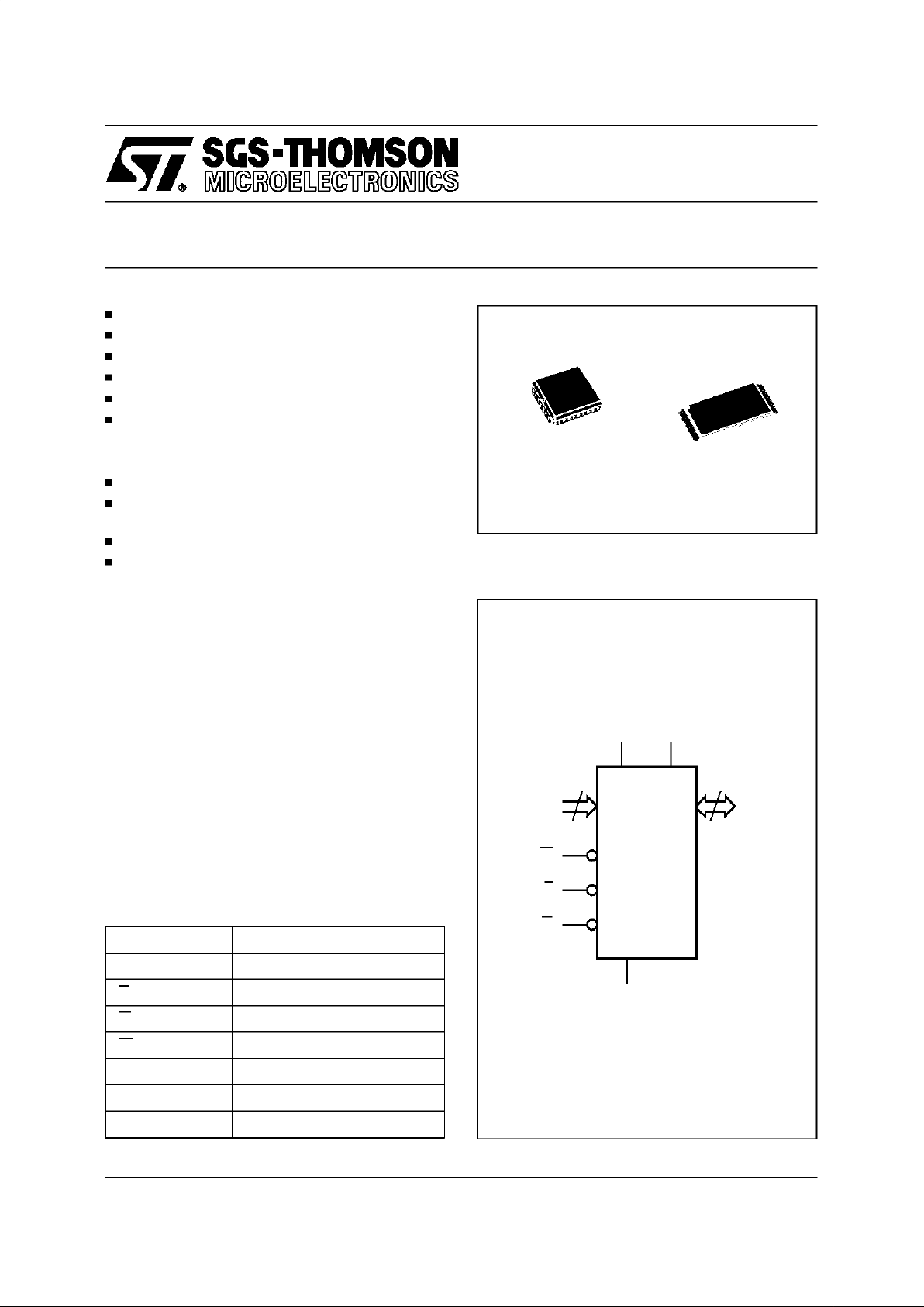
AI00637C
18
A0-A17
W
DQ0-DQ7
V
PP
V
CC
M28F201
G
E
V
SS
8
Figure 1. Logic Diagram
A0-A17 Address Inputs
DQ0-DQ7 Data Inputs / Outputs
E Chip Enable
G Output Enable
W Write Enable
V
PP
Program Supply
V
CC
SupplyVoltage
V
SS
Ground
Table 1. Signal Names
PLCC32 (K) TSOP32 (N)
8 x 20 mm
5V ± 10% SUPPLYVOLTAGE
12V PROGRAMMINGVOLTAGE
FASTACCESSTIME: 70ns
BYTEPROGRAMMINGTIME: 10µs typical
ELECTRICALCHIP ERASEin 1s RANGE
LOW POWERCONSUMPTION
– ActiveCurrent: 15mAtypical
– Stand-byCurrent: 10µAtypical
10,000PROGRAM/ERASE CYCLES
INTEGRATED ERASE/PROGRAM-STOP
TIMER
OTPCOMPATIBLE PACKAGESand PINOUTS
ELECTRONIC SIGNATURE
– ManufacturerCode: 20h
– DeviceCode: F4h
DESCRIPTION
The M28F201 FLASH Memory product is a nonvolatilememorieswhich may be erasedelectrically
at the chip level and programmed byte-by-byte. It
is organised as 256K bytes. It uses a command
registerarchitectureto select theoperating modes
and thus provide a simple microprocessor interface. The M28F201 FLASH Memory product is
suitablefor applicationswhere the memoryhas to
be reprogrammed in the equipment. The access
time of 70ns makes the device suitable for use in
high speed microprocessorsystems.
Page 2
AI00638C
A17
A13
A10
DQ5
17
A1
A0
DQ0
DQ1
DQ2
DQ3
DQ4
A7
A4
A3
A2
A6
A5
9
W
A8
1
A16
A9
DQ7
A12
A14
32
VPPV
CC
M28F201
A15
A11
DQ6
G
E
25
V
SS
Figure2A. LCCPin Connections
A1
A0
DQ0
A7
A4 A3
A2
A6
A5
A13
A10
A8
A9
DQ7
A14
A11 G
E
DQ5
DQ1
DQ2
DQ3
DQ4
DQ6
A17
W
A16
A12
V
PP
V
CC
A15
AI00639C
M28F201
(Normal)
8
1
9
16 17
24
25
32
V
SS
Figure 2B. TSOPPin Connections
DEVICEOPERATION
TheM28F201 FLASHMemory product employsa
technologysimilar to a 2 Megabit EPROM but add
to the device functionality by providing electrical
erasure and programming. These functions are
managed by a command register. The functions
that are addressed via the command register depend on the voltage applied to the V
PP
, program
voltage, input. When V
PP
is less than or equal to
6.5V, the command register is disabled and the
M28F201functionsas a readonly memoryproviding operating modessimilar to anEPROM (Read,
Output Disable, Electronic Signature Read and
Standby).WhenV
PP
israisedto 12Vthecommand
register is enabled and this provides, in addition,
Eraseand Program operations.
READONLYMODES, V
PP
≤ 6.5V
For all Read Only Modes, except StandbyMode,
the Write Enable input W should be High. In the
StandbyMode this input is ’don’tcare’.
ReadMode. TheM28F201has twoenableinputs,
E and G, both of which must be Low in order to
outputdata from thememory. TheChipEnable(E)
isthe powercontroland shouldbe usedfor device
selection. Output Enable (G) is the output control
and should be used to gatedata on to the output,
independantof the deviceselection.
A1
A0
DQ0
A7
A4A3
A2
A6
A5
A13
A10
A8
A9
DQ7
A14
A11G
E
DQ5
DQ1
DQ2
DQ3
DQ4
DQ6
A17
W
A16
A12
V
PP
V
CC
A15
AI00640D
M28F201
(Reverse)
8
9
16 17
24
25
V
SS
321
Figure2C. TSOPReverse Pin Connections
2/21
M28F201
Page 3
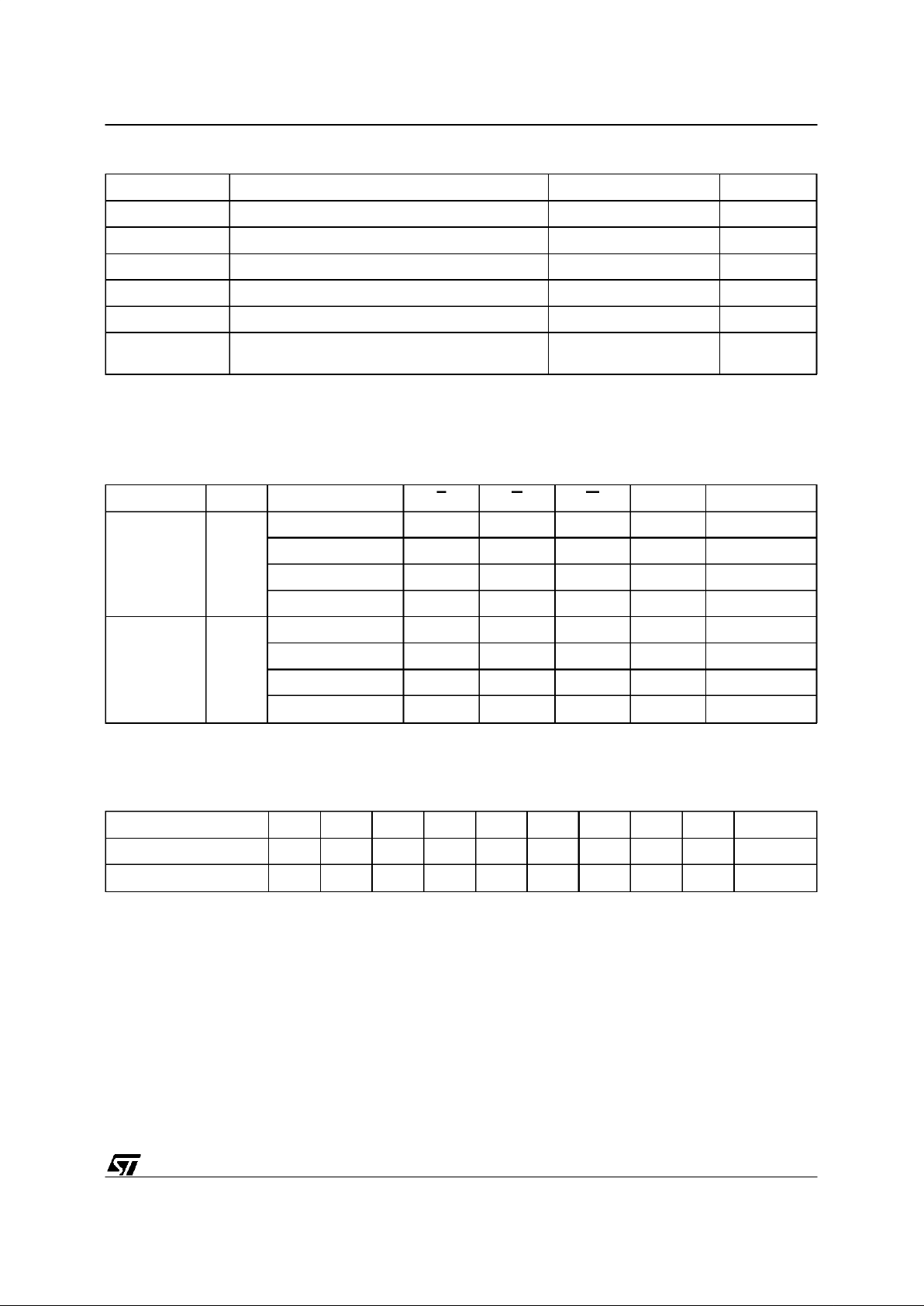
Symbol Parameter Value Unit
T
A
Ambient Operating Temperature –40 to125 °C
T
STG
Storage Temperature –65 to150 °C
V
IO
Input or Output Voltages –0.6 to 7 V
V
CC
Supply Voltage –0.6 to 7 V
V
A9
A9 Voltage –0.6 to 13.5 V
V
PP
Program Supply Voltage, during Erase
or Programming
–0.6 to 14 V
Note: Except for therating ”Operating Temperature Range”, stressesabove those listed in the Table”AbsoluteMaximum Ratings” may
cause permanent damage tothe device. These are stress ratings onlyand operation of the device at these or any other conditions above
those indicated in the Operating sections of this specificationis notimplied. Exposure to AbsoluteMaximum Ratingconditions for extended
periods may affect device reliability.Refer also to the SGS-THOMSON SURE Program and otherrelevant quality documents.
Table 2. AbsoluteMaximumRatings
Identifier A0 DQ7 DQ6 DQ5 DQ4 DQ3 DQ2 DQ1 DQ0 Hex Data
Manufacturer’s Code V
IL
00100000 20h
Device Code V
IH
11110100 F4h
Table 4. Electronic Signature
V
PP
Operation E G W A9 DQ0 - DQ7
ReadOnly V
PPL
Read V
IL
V
IL
V
IH
A9 Data Output
Output Disable V
IL
V
IH
V
IH
X Hi-Z
Standby V
IH
X X X Hi-Z
Electronic Signature V
IL
V
IL
V
IH
V
ID
Codes
Read/Write
(2)
V
PPH
Read V
IL
V
IL
V
IH
A9 Data Output
Write V
IL
V
IH
VILPulse A9 Data Input
Output Disable V
IL
V
IH
V
IH
X Hi-Z
Standby V
IH
X X X Hi-Z
Notes: 1. X = VILor VIH.
2. Refer also to the Command table.
Table 3. Operations
(1)
3/21
M28F201
Page 4
Command Cycles
1st Cycle 2nd Cycle
Operation A0-A17 DQ0-DQ7 Operation A0-A17 DQ0-DQ7
Read 1 Write X 00h
Electronic
Signature
(2)
2 Write X 80h or 90h
Read 00000h 20h
Read 00001h F4h
Setup Erase/
2
Write X 20h
Erase Write X 20h
Erase Verify 2 Write A0-A17 A0h Read X Data Output
Setup Program/
2
Write X 40h
Program Write A0-A17 Data Input
Program Verify 2 Write X C0h Read X Data Output
Reset 2 Write X FFh Write X FFh
Notes: 1. X = VILor VIH.
2. Refer also to the Electronic Signaturetable.
Table 5. Commands
(1)
Standby Mode. In the Standby Mode the maxi-
mum supply current is reduced. The device is
placed in the Standby Mode by applying a High
level to the Chip Enable (E) input. When in the
StandbyModetheoutputsare ina highimpedance
state, independantof theOutput Enable (G)input.
Output Disable Mode. When the Output Enable
(G) is High the outputs are in a high impedance
state.
ElectronicSignatureMode.Thismodeallowsthe
readout of two binary codesfromthe device which
identify the manufacturer and device type. This
mode is intended for use by programming equipment to automaticallyselect the correct eraseand
programmingalgorithms.The ElectronicSignature
Mode is activewhen a highvoltage (11.5Vto 13V)
isapplied toaddresslineA9withEandG Low.With
A0 Low the output data is the manufacturercode,
when A0 isHigh the output is thedevice code. All
other address lines should be maintained Low
while reading the codes. The electronicsignature
canalso be accessed in Read/Writemodes.
READ/WRITE MODES, 11.4V≤ V
PP
≤12.6V
When V
PP
is High both read and write operations
may be performed. These are defined by thecontents ofan internalcommand register.Commands
may be written to this register to set-up and execute,Erase,EraseVerify,Program,Program Verify
and Reset modes. Each of these modes needs 2
cycles. Each mode starts with a write operationto
set-upthe command,thisis followedby eitherread
or write operations. The device expects the first
cycle to be a write operation and doesnot corrupt
data at any location in the memory.Read modeis
set-upwith one cycle onlyand maybe followedby
any number of read operations to output data.
ElectronicSignatureRead modeis set-upwithone
cycle and followed by a read cycle to output the
manufactureror device codes.
Awriteto thecommandregisterismadebybringing
WLowwhileEisLow.ThefallingedgeofWlatches
Addresses, while the rising edge latches Data,
which are used for those commands that require
address inputs, command input or provide data
output. The supply voltage V
CC
and the program
voltageV
PP
canbe applied in any order. Whenthe
device is powered up or when V
PP
is ≤ 6.5V the
contentsof thecommand register defaultsto 00h,
thus automatically setting-up Read operations. In
addition a specific command may be used to set
the commandregisterto 00h for readingthe memory. The system designer may chose to provide a
constanthigh V
PP
anduse the registercommands
for all operations,or to switch the V
PP
from low to
high only when needing to erase or program the
memory. All command registeraccess is inhibited
whenV
CC
fallsbelowthe Erase/WriteLockoutVolt-
age (V
LKO
) of 2.5V.
If the device is deselected during Erasure, Programming or verifying it will draw active supply
currentsuntil the operationsare terminated.
The device is protected against stress caused by
long erase or programtimes.If theend ofErase or
Programming operations are not terminated by a
Verifycycle within a maximumtime permitted, an
internal stop timer automatically stops the operation.The deviceremainsin aninactivestate, ready
to start a Verifyor ResetMode operation.
4/21
M28F201
Page 5
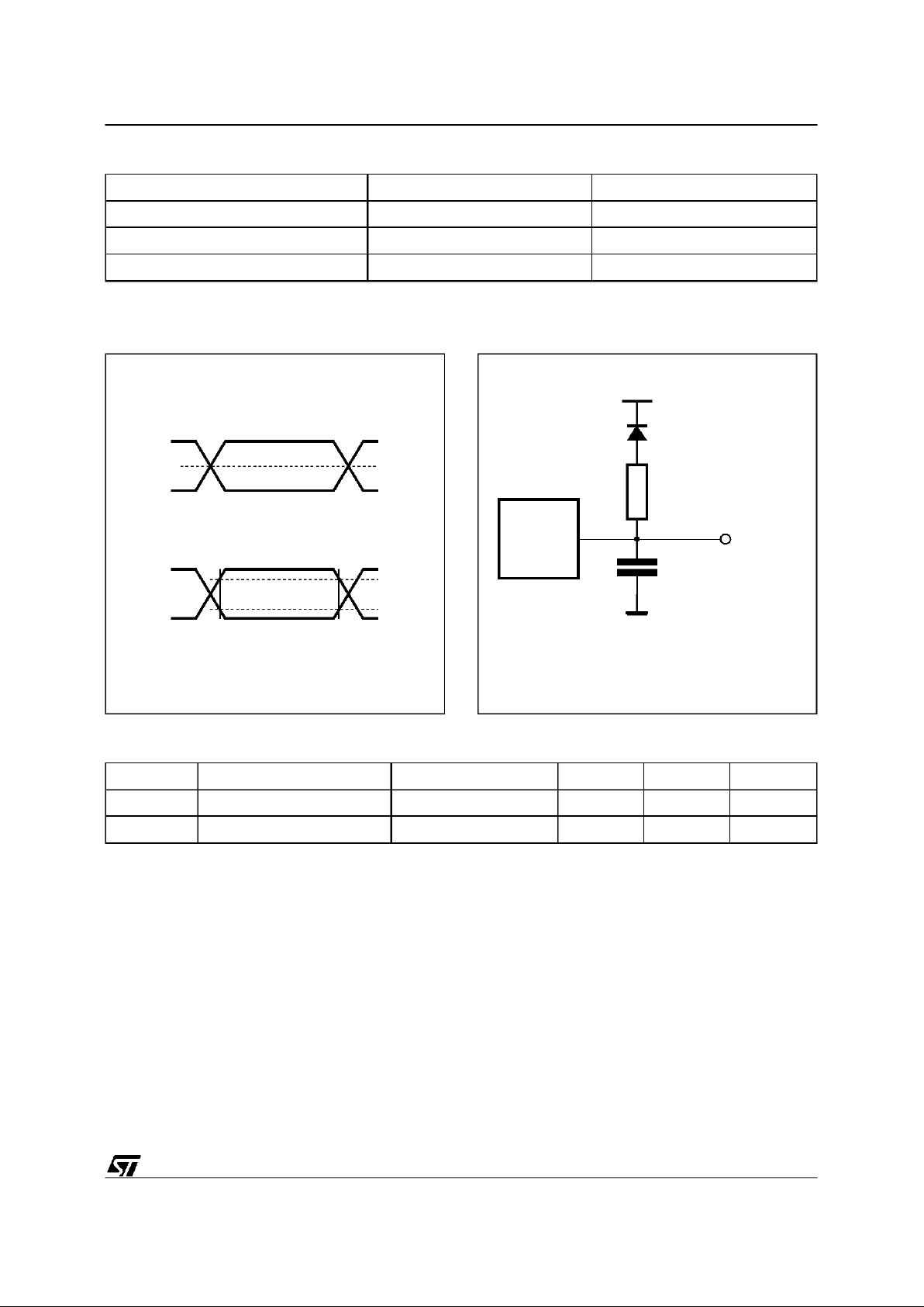
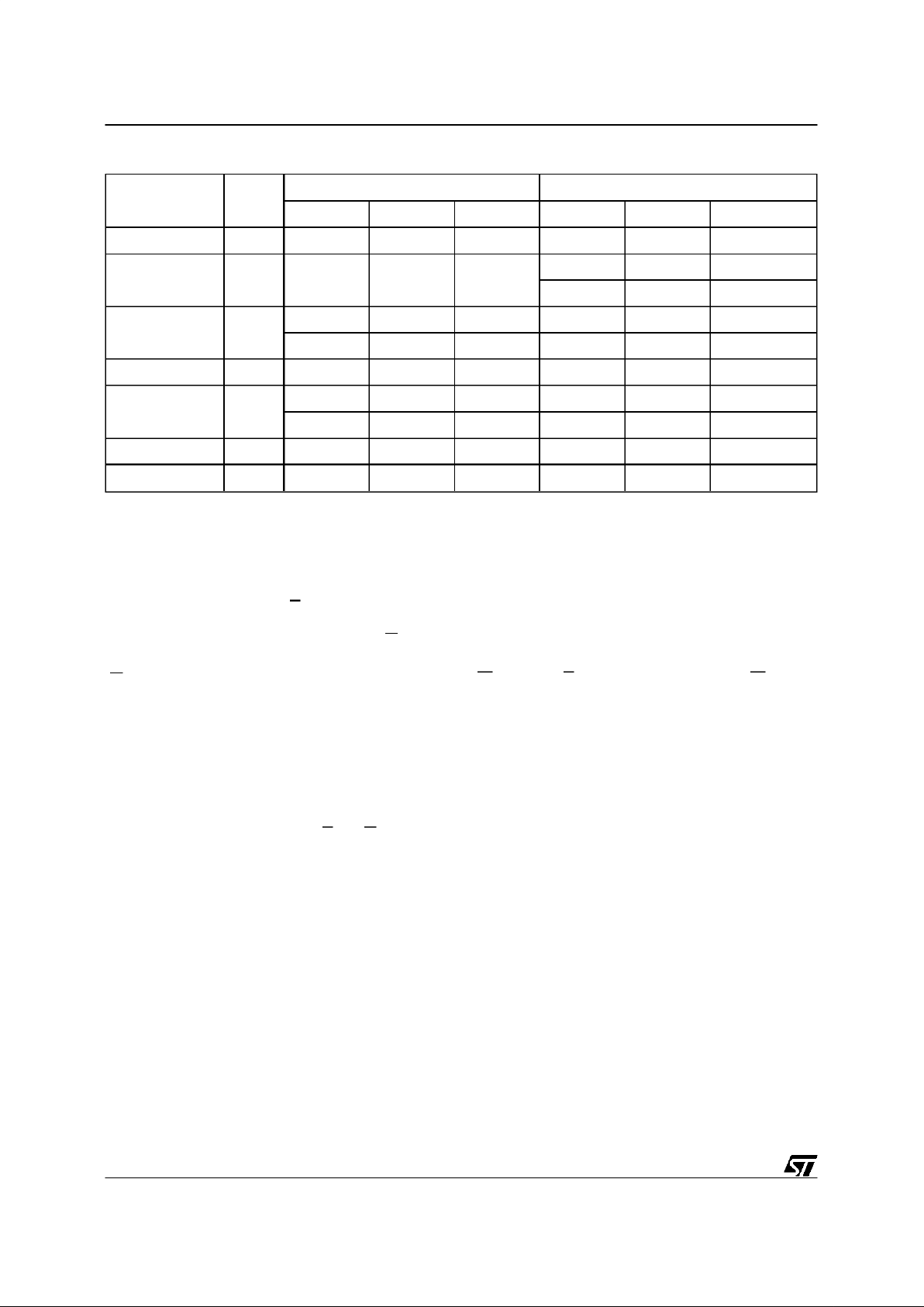
SRAM Interface Levels EPROM Interface Levels
Input Rise and Fall Times ≤ 10ns ≤ 10ns
Input PulseVoltages 0 to 3V 0.45V to 2.4V
Input and Output Timing Ref. Voltages 1.5V 0.8Vand 2V
Table 6. AC Measurement Conditions
AI01275
3V
SRAM Interface
0V
1.5V
2.4V
EPROM Interface
0.45V
2.0V
0.8V
Figure3. AC Testing Input Output Waveform
AI01276
1.3V
OUT
CL= 30pF or 100pF
CL= 30pF for SRAM Interface
CL= 100pF for EPROM Interface
CLincludes JIG capacitance
3.3kΩ
1N914
DEVICE
UNDER
TEST
Figure4. AC Testing Load Circuit
Symbol Parameter TestCondition Min Max Unit
C
IN
Input Capacitance VIN=0V 6 pF
C
OUT
Output Capacitance V
OUT
=0V 12 pF
Note: 1. Sampled only, not 100% tested.
Table 7. Capacitance
(1)
(TA=25°C, f = 1 MHz )
Read Mode. The Read Mode is the default at
power up or may be set-up by writing 00h to the
command register. Subsequent read operations
outputdatafromthememory.Thememoryremains
in the Read Mode until a new command is written
to the commandregister.
ElectronicSignatureMode. Inorder to select the
correcterase and programmingalgorithmsfor onboard programming,the manufacturerand device
codesmay be read directly. It isnot neccessaryto
apply a high voltage to A9 when using the command register. The Electronic Signature Mode is
set-up by writing 80h or 90h to the command
register. The following read cycles, with address
inputs00000hor 00001h,outputthe manufacturer
or device codes. The command is terminated by
writing another valid command to the command
register(for exampleReset).
5/21
M28F201
Page 6
Symbol Parameter Test Condition Min Max Unit
I
LI
Input LeakageCurrent 0V ≤ VIN≤ V
CC
±1 µA
I
LO
Output Leakage Current 0V ≤ V
OUT
≤ V
CC
±10 µA
I
CC
Supply Current (Read) E = VIL, f = 10MHz 30 mA
I
CC1
Supply Current (Standby) TTL E = V
IH
1mA
Supply Current (Standby) CMOS E = V
CC
± 0.2V 100 µA
I
CC2
(1)
Supply Current (Programming) During Programming 10 mA
I
CC3
(1)
Supply Current (Program Verify) During Verify 20 mA
I
CC4
(1)
Supply Current (Erase) During Erasure 20 mA
I
CC5
(1)
Supply Current (Erase Verify) During Erase Verify) 20 mA
I
LPP
Program Leakage Current VPP≤ V
CC
±10 µA
I
PP
Program Current (Read or
Standby)
V
PP>VCC
200 µA
V
PP
≤ V
CC
±10 µA
I
PP1
(1)
Program Current (Programming) VPP=V
PPH
, During Programming 30 mA
I
PP2
(1)
Program Current (Program
Verify)
V
PP=VPPH
, During Verify 5 mA
I
PP3
(1)
Program Current (Erase) VPP=V
PPH
, During Erase 30 mA
I
PP4
(1)
Program Current (Erase Verify) VPP=V
PPH
, DuringErase Verify 5 mA
V
IL
Input Low Voltage –0.5 0.8 V
V
IH
Input High VoltageTTL 2 VCC+ 0.5 V
Input High Voltage CMOS 0.7 V
CC
VCC+ 0.5 V
V
OL
Output Low Voltage IOL= 5.8mA 0.45 V
V
OH
Output High Voltage CMOS
I
OH
= –100µAV
CC
– 0.4 V
I
OH
= –2.5mA 0.85 V
CC
V
Output High VoltageTTL I
OH
= –2.5mA 2.4 V
V
PPL
Program Voltage(Read
Operations)
0 6.5 V
V
PPH
Program Voltage(Read/Write
Operations)
11.4 12.6 V
V
ID
A9 Voltage(Electronic Signature) 11.5 13 V
I
ID
(1)
A9 Current (Electronic Signature) A9 = V
ID
200 µA
V
LKO
Supply Voltage,Erase/Program
Lock-out
2.5 V
Note: 1. Not 100% tested. Characterisation Data available.
Table 8. DC Characteristics
(T
A
= 0 to 70 °C, –40 to 85 °C or –40to 125 °C; VCC=5V±10%)
6/21
M28F201
Page 7
Symbol Alt Parameter Test Condition
M28F201
Unit
-70 -90 -120 -150
V
CC
=
5V±10%
VCC=
5V±10%
VCC=
5V±10%
VCC=
5V±10%
EPROM
Interface
EPROM
Interface
EPROM
Interface
EPROM
Interface
Min Max Min Max Min Max Min Max
t
WHGL
Write Enable High to
Output EnableLow
6666µs
t
AVAV
t
RC
Read Cycle Time E = VIL,G=VIL70 90 120 150 ns
t
AVQV
t
ACC
Address Validto
Output Valid
E=V
IL
,G=V
IL
70 90 120 150 ns
t
ELQX
(1)
t
LZ
Chip Enable Low to
Output Transition
G=V
IL
0000ns
t
ELQV
t
CE
Chip Enable Low to
Output Valid
G=V
IL
70 90 120 150 ns
t
GLQX
(1)
t
OLZ
Output EnableLow
to Output Transition
E=V
IL
0000ns
t
GLQV
t
OE
Output EnableLow
to Output Valid
E=V
IL
25 30 35 40 ns
t
EHQZ
(1)
Chip Enable High to
Output Hi-Z
G=V
IL
0 25 0 30 0 30 0 35 ns
t
GHQZ
(1)
t
DF
Output EnableHigh
to Output Hi-Z
E=V
IL
0 25 0 30 0 30 0 35 ns
t
AXQX
t
OH
Address Transition
to Output Transition
E=V
IL
,G=VIL0000ns
Note: 1. Sampled only,not 100% tested
Table9. Read Only Mode AC Characteristics
((T
A
= 0 to 70 °C, –40 to 85 °C or –40 to 125 °C)
Erase and Erase Verify Modes. The memory is
erased by first Programming all bytes to 00h,the
Erase command then erases them to FFh. The
Erase Verify command is then used to read the
memory byte-by-byte for a content of FFh. The
Erase Mode is set-up by writing 20h to the command register. The write cycle is then repeated to
start the erase operation. Erasure starts on the
rising edge of W duringthis second cycle.Eraseis
followed by an Erase Verify which reads an addressed byte. Erase VerifyMode is set-up bywriting A0h tothe command register and at thesame
time supplying the address of the byte to be verified. The rising edge of W duringthe set-up of the
firstErase VerifyMode stops theEraseoperation.
Thefollowing read cycle is madewith an internally
generated margin voltage applied; reading FFh
indicatesthatallbitsof theaddressedbyte arefully
erased. The whole contents of the memory are
verified by repeating the Erase Verify Operation,
first writing the set-up code A0h with the address
of thebyte to be verified and thenreadingthe byte
contentsin a secondread cycle.
As the Erasealgorithm flow chart shows,when the
data read during Erase Verify is not FFh, another
Eraseoperation is performedand verificationcontinuesfromtheaddressofthelast verifiedbyte.The
command is terminated by writing another valid
command to the command register (for example
Programor Reset).
7/21
M28F201
Page 8

AI00642
tAVAV
tAVQV tAXQX
tELQV
tELQX
tEHQZ
tGLQV
tGLQX
tGHQZ
DATA OUT
A0-A17
E
G
DQ0-DQ7
Figure5. Read Mode AC Waveforms
AI00643
tWHGL
tVPHEL
VALID
tELQV tEHQZ
tAVQV
A0-A17
E
G
DQ0-DQ7 DATA OUTCOMMAND
V
PP
W
tAXQX
tGHQZ
tGLQV
READREAD SET-UP
tWLWH
tWHDXtDVWH
tGHWL
tELWL tWHEH
Figure6. Read Command Waveforms
8/21
M28F201
Page 9

AI00644
tWHGL
tVPHEL
00000h-00001h
tELQV tEHQZ
tAVQV
A0-A17
E
G
DQ0-DQ7 DATA OUTCOMMAND
V
PP
W
tAXQX
tGHQZ
tGLQV
READ
MANUFACTURER
OR DEVICE
READ
ELECTRONIC
SIGNATURE SET-UP
tWLWH
tWHDXtDVWH
tGHWL
tELWL tWHEH
Figure7. Electronic Signature Command Waveforms
Program and Program Verify Modes. The Pro-
gramModeisset-upbywriting40htothe command
register. This is followed by a second write cycle
which latchesthe addressand data of thebyte to
be programmed.The risingedge of W during this
second cycle starts the programming operation.
ProgrammingisfollowedbyaProgramVerifyofthe
data written.
ProgramVerifyModeisset-upbywritingC0hto the
commandregister.The rising edgeof Wduring the
set-up of the Program Verify Mode stopsthe Pro-
gramming operation. The followingread cycle, of
the address already latched during programming,
is made with an internallygenerated margin voltageapplied,readingvaliddataindicatesthatallbits
have been programmed.
ResetMode.Thiscommandisusedtosafely abort
Erase or Program Modes. The Reset Mode is
set-up and performed by writing FFh two times to
the command register. The command should be
followed by writing a valid command to the the
commandregister (for exampleRead).
9/21
M28F201
Page 10

Symbol Alt Parameter
M28F201
Unit
-70 -90
V
CC
=5V±10% VCC=5V±10%
EPROM
Interface
EPROM
Interface
Min Max Min Max
t
VPHEL
VPPHigh to Chip Enable Low 1 1 µs
t
VPHWL
VPPHigh to Write Enable Low 1 1 µs
t
WHWH3tWC
Write Cycle Time(W controlled) 70 90 ns
t
EHEH3
t
WC
Write Cycle Time(E controlled) 70 90 ns
t
AVWL
t
AS
Address Valid to Write Enable Low 0 0 ns
t
AVEL
Address Valid to Chip Enable Low 0 0 ns
t
WLAX
t
AH
Write Enable Low to Address Transition 30 45 ns
t
ELAX
Chip Enable Low to Address Transition 30 45 ns
t
ELWL
t
CS
Chip Enable Low to Write Enable Low 0 0 ns
t
WLEL
Write Enable Low to Chip Enable Low 0 0 ns
t
GHWL
Output Enable High to Write Enable Low 0 0 µs
t
GHEL
Output Enable High to ChipEnable Low 0 0 µs
t
DVWH
t
DS
Input Valid to Write Enable High 30 45 ns
t
DVEH
Input Valid to Chip Enable High 30 45 ns
t
WLWH
t
WP
Write Enable Low to WriteEnable High (Write Pulse) 30 45 ns
t
ELEH
Chip Enable Low to Chip Enable High (Write Pulse) 50 60 ns
t
WHDX
t
DH
Write Enable High to InputTransition 10 10 ns
t
EHDX
Chip Enable High to Input Transition 10 10 ns
t
WHWH1
Duration of Program Operation (W contr.) 10 10 µs
t
EHEH1
Duration of Program Operation (E contr.) 10 10 µs
t
WHWH2
Duration of Erase Operation (W contr.) 9.5 9.5 ms
t
EHEH2
Duration of Erase Operation (E contr.) 9.5 9.5 ms
t
WHEH
t
CH
Write Enable High to Chip Enable High 0 0 ns
t
EHWH
Chip Enable High to Write Enable High 0 0 ns
t
WHWLtWPH
Write Enable High to Write Enable Low 10 20 ns
t
EHEL
Chip Enable High to Chip Enable Low 10 20 ns
t
WHGL
Write Enable High to Output EnableLow 6 6 µs
t
EHGL
Chip Enable High to Output Enable Low 6 6 µs
t
AVQV
t
ACC
Addess Validto data Output 70 90 ns
t
ELQX
(1)
t
LZ
Chip Enable Low to Output Transition 0 0 ns
t
ELQV
t
CE
Chip Enable Low to Output Valid 70 90 ns
t
GLQX
(1)
t
OLZ
Output Enable Low to Output Transition 0 0 ns
t
GLQV
t
OE
Output Enable Low to Output Valid 25 30 ns
t
EHQZ
(1)
Chip Enable High to Output Hi-Z 25 30 ns
t
GHQZ
(1)
t
DF
Output Enable High to Output Hi-Z 25 30 ns
t
AXQX
t
OH
Address Transition to Output Transition 0 0 ns
Note: 1. Sampled only,not 100% tested
Table 10A. Read/Write Mode AC Characteristics,W and E Controlled
(T
A
= 0 to 70 °C, –40 to 85 °C or –40to 125 °C)
10/21
M28F201
Page 11

Symbol Alt Parameter
M28F201
Unit
-120 -150
V
CC
=5V±10% VCC=5V±10%
EPROM
Interface
EPROM
Interface
Min Max Min Max
t
VPHEL
VPPHigh to Chip Enable Low 1 1 µs
t
VPHWL
VPPHigh to Write Enable Low 1 1 µs
t
WHWH3tWC
Write Cycle Time(W controlled) 120 150 ns
t
EHEH3
t
WC
Write Cycle Time(E controlled) 120 150 ns
t
AVWL
t
AS
Address Valid to Write Enable Low 0 0 ns
t
AVEL
Address Valid to Chip Enable Low 0 0 ns
t
WLAX
t
AH
Write Enable Low to Address Transition 50 50 ns
t
ELAX
Chip Enable Low to Address Transition 60 80 ns
t
ELWL
t
CS
Chip Enable Low to Write Enable Low 0 0 ns
t
WLEL
Write Enable Low to Chip Enable Low 0 0 ns
t
GHWL
Output Enable High to Write Enable Low 0 0 µs
t
GHEL
Output Enable High to ChipEnable Low 0 0 µs
t
DVWH
t
DS
Input Valid to Write Enable High 50 50 ns
t
DVEH
Input Valid to Chip Enable High 50 50 ns
t
WLWH
t
WP
Write Enable Low to WriteEnable High (Write Pulse) 50 60 ns
t
ELEH
Chip Enable Low to Chip Enable High (Write Pulse) 70 80 ns
t
WHDX
t
DH
Write Enable High to InputTransition 10 10 ns
t
EHDX
Chip Enable High to Input Transition 10 10 ns
t
WHWH1
Duration of Program Operation (W contr.) 10 10 µs
t
EHEH1
Duration of Program Operation (E contr.) 10 10 µs
t
WHWH2
Duration of Erase Operation (W contr.) 9.5 9.5 ms
t
EHEH2
Duration of Erase Operation (E contr.) 9.5 9.5 ms
t
WHEH
t
CH
Write Enable High to Chip Enable High 0 0 ns
t
EHWH
Chip Enable High to Write Enable High 0 0 ns
t
WHWLtWPH
Write Enable High to Write Enable Low 20 20 ns
t
EHEL
Chip Enable High to Chip Enable Low 20 20 ns
t
WHGL
Write Enable High to Output EnableLow 6 6 µs
t
EHGL
Chip Enable High to Output Enable Low 6 6 µs
t
AVQV
t
ACC
Addess Validto data Output 120 150 ns
t
ELQX
(1)
t
LZ
Chip Enable Low to Output Transition 0 0 ns
t
ELQV
t
CE
Chip Enable Low to Output Valid 120 150 ns
t
GLQX
(1)
t
OLZ
Output Enable Low to Output Transition 0 0 ns
t
GLQV
t
OE
Output Enable Low to Output Valid 35 40 ns
t
EHQZ
(1)
Chip Enable High to Output Hi-Z 30 35 ns
t
GHQZ
(1)
t
DF
Output Enable High to Output Hi-Z 30 35 ns
t
AXQX
t
OH
Address Transition to Output Transition 0 0 ns
Note: 1. Sampled only,not 100% tested
Table 10B. Read/Write Mode AC Characteristics,W and E Controlled
(T
A
= 0 to 70 °C, –40 to 85 °C or –40to 125 °C)
11/21
M28F201
Page 12

AI00645
tWHEH
tVPHEL
VALID
tELQV tEHQZ
tAVWL
A0-A17
E
G
DQ0-DQ7 COMMAND
V
PP
W
tWLAX
tGHQZtWHWH2
VERIFY
READ
ERASE SET-UP
tWLWH
tWHDXtDVWH
tGHWL
tELWL tWHEH
COMMAND
tWHGLtWHWL
COMMAND
tWHDXtDVWH
DATA OUT
tWHWH3
ERASE OPERATION
tWLWH tGLQV
ERASE SET-UP
(REPEAT OF 1st CYCLE)
ERASE VERIFY
SET-UP
tELWL
Figure8. Erase Set-up and Erase VerifyCommands Waveforms,W Controlled
12/21
M28F201
Page 13

AI01328
tEHWH
tVPHWL
VALID
tGLQV
tEHQZ
tAVEL
A0-A17
W
G
DQ0-DQ7 COMMAND
V
PP
E
tELAX
tGHQZtEHEH2
VERIFY
READ
ERASE SET-UP
tELEH
tEHDXtDVEH
tGHEL
tWLEL tEHWH
COMMAND
tEHGLtEHEL
COMMAND
tEHDXtDVEH
DATA OUT
tEHEH3
ERASE OPERATION
tELEH tELQV
ERASE SET-UP
(REPEAT OF 1st CYCLE)
ERASE VERIFY
SET-UP
tWLEL
Figure9. Erase Set-upandErase Verify Commands Waveforms, EControlled
13/21
M28F201
Page 14

AI00646
tWHEH
tVPHEL
VALID
tELQV tEHQZ
tAVWL
A0-A17
E
G
DQ0-DQ7 COMMAND
V
PP
W
tWLAX
tGHQZ
tWHWH1
VERIFY
READ
PROGRAM SET-UP
tWLWH
tWHDX
tDVWH
tGHWL
tELWL tWHEH
DATA IN
tWHGLtWHWL
COMMAND
tWHDXtDVWH
DATA OUT
tWHWH3
PROGRAM OPERATION
tWLWH tGLQV
ADDRESS AND
DATA LATCH
PROGRAM
VERIFY SET-UP
tELWL
tWHDX
tDVWH
tELWL
tWLWH
tWHEH
Figure10. ProgramSet-up and ProgramVerify Commands Waveforms- W Controlled
14/21
M28F201
Page 15

AI00648
tEHWH
tVPHEL
VALID
tELQV tEHQZ
tAVEL
A0-A17
G
DQ0-DQ7 COMMAND
V
PP
W
tELAX
tGHQZ
tEHEH1
VERIFY
READ
PROGRAM SET-UP
tELEH
tEHDX
tDVEH
tGHEL
tWLEL tEHWH
DATA IN
tEHGLtEHEL
COMMAND
tEHDXtDVEH
DATA OUT
tEHEH3
PROGRAM OPERATION
tELEH
tGLQV
ADDRESS AND
DATA LATCH
PROGRAM
VERIFY SET-UP
tWLEL
tEHDX
tDVEH
tWLEL
tELEH
tEHWH
E
Figure11. ProgramSet-up and Program Verify Commands Waveforms - E Controlled
15/21
M28F201
Page 16

PRESTOF ERASEALGORITHM
The PRESTO F Erase Algorithm guarantees that
the device will be erased in a reliable way. The
algorithmfirstprogramsall bytes to 00h inorderto
ensureuniform erasure. The programmingfollows
the PRESTO F Programming Algorithm. Erase is
set-up by writing 20h to thecommand register,the
erasure is started by repeating this write cycle.
Erase Verify is set-up by writing A0h to the commandregister togetherwith the addressofthebyte
tobeverified.The subsequentreadcyclereadsthe
datawhichiscomparedtoFFh.Erase Verifybegins
ataddress0000h andcontinuesto the lastaddress
or until the comparisonof the data to FFh fails. If
this occurs, the address of the lastbyte checkedis
stored and a new Erase operation performed.
EraseVerifythencontinuesfromthe addressof the
stored location.
PRESTOF PROGRAM ALGORITHM
ThePRESTO F ProgrammingAlgorithm appliesa
series of10µs programmingpulses to a byte until
a correct verify occurs. Up to 25 programming
operations are allowed for one byte. Program is
set-upby writing 40h to thecommandregister,the
programming is started after the next write cycle
which also latches the address and data to be
programmed. Program Verify is set-up by writing
C0h to the commandregister, followed by a read
cycle and a compareof thedata read to the data
expected.DuringProgram and Program Verify operations a MARGIN MODE circuit is activated to
guaranteethatthecellisprogrammedwitha safety
margin.
PROGRAM
ALL
BYTES TO 00h
AI00649
n=0, Addr=00000h
Last
Addr
ERASE SET-UP
Wait 10ms
ERASE VERIFY
Latch Addr.
READ DATA OUTPUT
Data
OK
Wait 6µs
++n
=
Addr++
READ COMMAND
VPP= 12V
VPP<
6.5V
FAIL
VPP< 6.5V, PASS
YES
NO
YES
NO
YES
NO
1000
Figure12. Erasing Flowchart
AI00677
n=0
Last
Addr
PROGRAM VERIFY
Wait 10µs
PROGRAM SET-UP
Latch Addr, Data
READ DATAOUTPUT
Data
OK
Wait 6µs
++n
=25
Addr++
READ COMMAND
VPP= 12V
VPP<
6.5V
FAIL
VPP< 6.5V, PASS
YES
NO
YES
NO
YES
NO
Figure13. ProgrammingFlowchart
16/21
M28F201
Page 17

ORDERING INFORMATION SCHEME
Operating Voltage
F5V
Speed
-70 70ns
-90 90 ns
-120 120 ns
-150 150 ns
Power Supplies
blank V
CC
± 10%
XV
CC
± 5%
Package
K PLCC32
N TSOP32
8 x 20 mm
Option
R Reverse
Pinout
TR Tape& Reel
Packing
Temperature Range
1 0 to 70 °C
3 –40 to 125 °C
6 –40 to 85 °C
Example: M28F201 -70 X N 1 TR
Devicesare shippedfrom the factorywiththe memory content erased (to FFh).
Foralist ofavailableoptions(Speed,Package,etc...)orfor furtherinformationonany aspectof thisdevice,
pleasecontact the SGS-THOMSONSales Office nearestto you.
17/21
M28F201
Page 18

PLCC
D
Ne E1 E
1N
D1
Nd
CP
B
D2/E2
e
B1
A1
A
Symb
mm inches
Typ Min Max Typ Min Max
A 2.54 3.56 0.100 0.140
A1 1.52 2.41 0.060 0.095
B 0.33 0.53 0.013 0.021
B1 0.66 0.81 0.026 0.032
D 12.32 12.57 0.485 0.495
D1 11.35 11.56 0.447 0.455
D2 9.91 10.92 0.390 0.430
E 14.86 15.11 0.585 0.595
E1 13.89 14.10 0.547 0.555
E2 12.45 13.46 0.490 0.530
e 1.27 – – 0.050 – –
N32 32
Nd 7 7
Ne 9 9
CP 0.10 0.004
PLCC32
Drawing is notto scale.
PLCC32- 32 lead Plastic Leaded Chip Carrier, rectangular
18/21
M28F201
Page 19

TSOP-a
D1
E
1N
CP
B
e
A2
A
N/2
D
DIE
C
LA1 α
Symb
mm inches
Typ Min Max Typ Min Max
A 1.20 0.047
A1 0.05 0.17 0.002 0.006
A2 0.95 1.50 0.037 0.059
B 0.15 0.27 0.006 0.011
C 0.10 0.21 0.004 0.008
D 19.80 20.20 0.780 0.795
D1 18.30 18.50 0.720 0.728
E 7.90 8.10 0.311 0.319
e 0.50 – – 0.020 – –
L 0.50 0.70 0.020 0.028
α 0° 5° 0° 5°
N32 32
CP 0.10 0.004
TSOP32
Drawing is notto scale.
TSOP32 Normal Pinout - 32 lead Plastic Thin Small Outline, 8 x 20mm
19/21
M28F201
Page 20

Symb
mm inches
Typ Min Max Typ Min Max
A 1.20 0.047
A1 0.05 0.17 0.002 0.006
A2 0.95 1.50 0.037 0.059
B 0.15 0.27 0.006 0.011
C 0.10 0.21 0.004 0.008
D 19.80 20.20 0.780 0.795
D1 18.30 18.50 0.720 0.728
E 7.90 8.10 0.311 0.319
e 0.50 – – 0.020 – –
L 0.50 0.70 0.020 0.028
α 0° 5° 0° 5°
N32 32
CP 0.10 0.004
TSOP32
TSOP32 Reverse Pinout - 32 lead Plastic Thin Small Outline, 8 x 20mm
TSOP-b
D1
E
1N
CP
B
e
A2
A
N/2
D
DIE
C
LA1 α
Drawing is notto scale.
20/21
M28F201
Page 21

Information furnished isbelieved to be accurate and reliable.However, SGS-THOMSON Microelectronics assumes no responsibility for the
consequences of use of such information nor for any infringementof patents or other rights of third parties which may result from its use. No
license is granted by implication or otherwise under any patent or patent rights of SGS-THOMSON Microelectronics. Specifications mentioned
in this publication are subject to change without notice. This publication supersedes and replaces all information previously supplied.
SGS-THOMSON Microelectronics products are not authorized for use as critical componentsin life supportdevices or systemswithout express
written approval of SGS-THOMSON Microelectronics.
1997 SGS-THOMSON Microelectronics - All Rights Reserved
SGS-THOMSON Microelectronics GROUP OF COMPANIES
Australia - Brazil - Canada- China -France - Germany- Hong Kong - Italy -Japan - Korea- Malaysia - Malta - Morocco - The Netherlands -
Singapore- Spain - Sweden - Switzerland - Taiwan- Thailand - United Kingdom - U.S.A.
21/21
M28F201
 Loading...