

Datasheet M28F101-120N1, M28F101-100P1, M28F101-150P6, M28F101-150P1, M28F101-150K1 Datasheet (SGS Thomson Microelectronics)
Page 1
1 Mb (128K x 8, Chip Erase) FLASH MEMORY
5V ±10% SUPPLY VOLTAGE
12V PROGRAMMINGVOLTAGE
FASTACCESSTIME: 70ns
BYTEPROGRAMINGTIME: 10µs typical
ELECTRICALCHIP ERASE in 1s RANGE
LOW POWERCONSUMPTION
– Stand-byCurrent: 100µAmax
10,000ERASE/PROGRAM CYCLES
INTEGRATED ERASE/PROGRAM-STOP
TIMER
OTPCOMPATIBLE PACKAGESand PINOUTS
ELECTRONIC SIGNATURE
– ManufacturerCode: 20h
– DeviceCode: 07h
DESCRIPTION
The M28F101 FLASH Memory is a non-volatile
memory which may be erased electrically at the
chip level and programmed byte-by-byte. It is organisedas128K bytesof8 bits.It usesacommand
registerarchitectureto select the operating modes
and thus provides a simple microprocessor interface.The M28F101 FLASHMemory is suitablefor
applications where the memory has to be reprogrammed in the equipment. The access time of
70ns makes the device suitable for use in high
speedmicroprocessor systems.
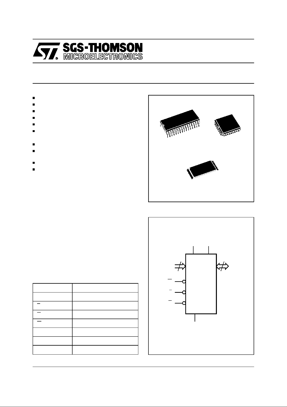
32
1
PDIP32 (P)
TSOP32 (N)
8 x 20 mm
Figure 1. Logic Diagram
V
CC
17
A0-A16
M28F101
PLCC32 (K)
V
PP
8
DQ0-DQ7
Table 1. Signal Names
A0-A16 Address Inputs
DQ0-DQ7 Data Inputs / Outputs
E Chip Enable
G Output Enable
W Write Enable
V
PP
V
CC
V
SS
April 1997 1/23
Program Supply
SupplyVoltage
Ground
W
M28F101
E
G
V
SS
AI00666B
Page 2
M28F101
Figure2A. DIP Pin Connections
V
1
PP
2
A15
3
A12
4
A7
5
A6
6
A5
7
A4
8
9
10
11
12
13
M28F101
A3
A2
A1
A0
DQ0
14
DQ2
15
16
SS
Warning: NC = Not Connected. Warning: NC = Not Connected.
32
31
30
29
28
27
26
25
24
23
22
21
20
19
18
17
AI00667
V
CC
WA16
NC
A14
A13
A8
A9
A11
G
A10
E
DQ7
DQ6
DQ5DQ1
DQ4
DQ3V
Figure2B. LCC Pin Connections
A16
A7
A6
A5
A4
A3
A2
A1
A0
DQ0
A12
9
DQ1
VPPV
A15
1
M28F101
17
SS
V
DQ2
DQ3
32
CC
DQ4
W
DQ5
NC
25
DQ6
A14
A13
A8
A9
A11
G
A10
E
DQ7
AI00668
Figure2C. TSOP Pin Connections
A11 G
A9
A8
A13
A14
NC
V
CC
V
PP
A16
A15
A12
A7
A6
A5
A4 A3
Warning: NC = Not Connected.
1
W
8
9
16 17
M28F101
(Normal)
32
25
24
AI00669B
A10
E
DQ7
DQ6
DQ5
DQ4
DQ3
V
SS
DQ2
DQ1
DQ0
A0
A1
A2
Figure2D. TSOP Reverse Pin Connections
1
A10
E
DQ7
DQ6
DQ5
DQ4
DQ3
V
SS
8
9
M28F101
(Reverse)
DQ2
DQ1
DQ0
A0
A1
A2
16 17
Warning: NC = Not Connected.
AI00670C
32
25
24
A11G
A9
A8
A13
A14
NC
W
V
CC
V
PP
A16
A15
A12
A7
A6
A5
A4A3
2/23
Page 3
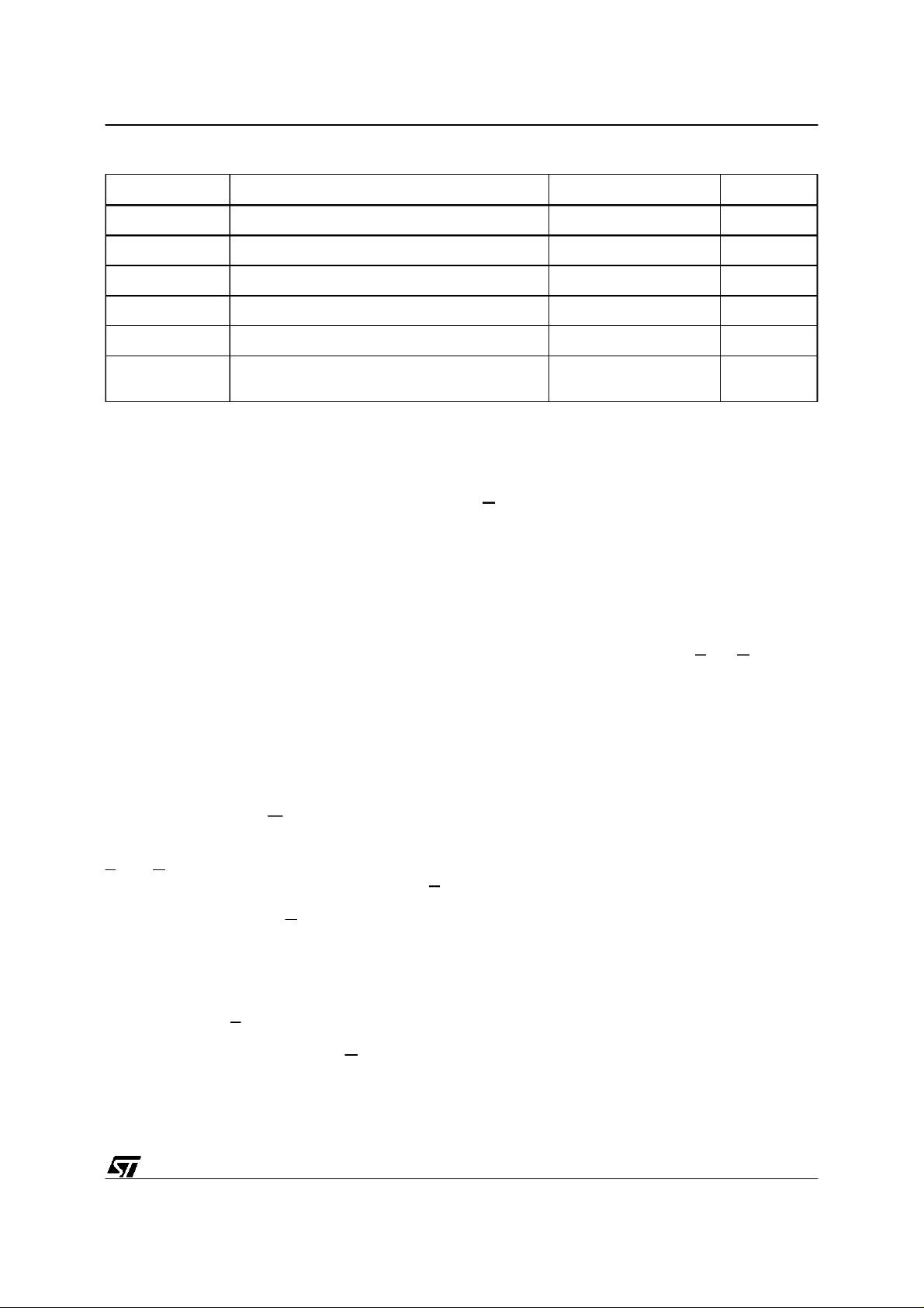
Table 2. AbsoluteMaximumRatings
Symbol Parameter Value Unit
M28F101
T
A
T
STG
V
IO
V
CC
V
A9
V
PP
Note: Except for therating ”Operating Temperature Range”, stressesabove those listed in the Table”Absolute Maximum Ratings” may
cause permanent damage to the device. These are stress ratings only and operation ofthe device at these or any otherconditions above
those indicated in the Operating sections of this specification is not implied. Exposure to Absolute Maximum Rating conditions for extended
periods may affect device reliability.Refer also to the SGS-THOMSON SURE Program and other relevant quality documents.
DEVICE OPERATION
The M28F101FLASHMemoryemploys a technologysimilar to a 1 MegabitEPROMbut adds to the
devicefunctionalityby providingelectrical erasure
and programming. These functions are managed
by a command register. The functions that are
addressed via the command register depend on
the voltage applied to the V
input. When V
commandregisteris disabled and M28F101functions as a read only memory providing operating
modes similar to an EPROM (Read, Output Disable, Electronic Signature Read and Standby).
When V
is raised to 12V the command regsiter
PP
isenabledand this provides,inaddition,Eraseand
Programoperations.
Ambient Operating Temperature –40 to 125 °C
Storage Temperature –65 to150 °C
Input or Output Voltages –0.6 to 7 V
Supply Voltage –0.6 to 7 V
A9 Voltage –0.6 to 13.5 V
Program Supply Voltage, during Erase
or Programming
–0.6 to 14 V
Output Disable Mode. When the Output Enable
(G) is High the outputs are in a high impedance
state.
ElectronicSignatureMode.Thismodeallowsthe
read outof two binarycodesfrom thedevice which
identify the manufacturer and device type. This
mode is intended for use by programming equip-
, program voltage,
is less than or equal to 6.5V,the
PP
PP
mentto automaticallyselect the correct erase and
programmingalgorithms.TheElectronicSignature
Modeis activewhen a high voltage (11.5Vto 13V)
isappliedto addresslineA9with EandG Low.With
A0 Low the output data is the manufacturercode,
whenA0 isHigh the outputis the devicetype code.
All other address lines should be maintained Low
while reading the codes. The electronicsignature
may also be accessedin Read/Write modes.
READONLYMODES, V
PP
≤ 6.5V
For all Read Only Modes, except Standby Mode,
the Write Enable input W should be High. In the
StandbyMode this input is don’t care.
ReadMode. TheM28F101has two enable inputs,
E and G, both of which must be Low in order to
output data from the memory. TheChipEnable (E)
is the powercontrol and shouldbe used for device
selection. Output Enable (G) is the output control
and should be used to gate data on to the output,
independantof the deviceselection.
Standby Mode. In the Standby Mode the maximum supply current is reduced. The device is
placedin the StandbyMode by applyinga High to
the Chip Enable (E) input. When in the Standby
Mode the outputs are in a high impedance state,
independantof the OutputEnable (G) input.
READ/WRITEMODES, 11.4V ≤ V
When V
is High both read and write operations
PP
≤ 12.6V
PP
may be performed. These are defined by the contents of an internal commandregister.Commands
may be written to this register to set-up and execute,Erase,EraseVerify,Program,ProgramVerify
and Reset modes. Each of these modes needs 2
cycles. Eah mode starts with a write operation to
set-upthe command,this is followedbyeither read
or write operations. The device expects the first
cycle to be a writeoperation and does not corrupt
data at any location in the memory.Read mode is
set-upwith one cycleonly and may be followed by
any number of read operations to output data.
ElectronicSignatureRead modeis set-up with one
cycle and followed by a read cycle to output the
manufactureror devicecodes.
3/23
Page 4
M28F101
Table 3. Operations
ReadOnly V
(1)
V
PP
PPL
Operation E G W A9 DQ0 - DQ7
Output Disable V
Electronic Signature V
(2)
Read/Write
V
PPH
Output Disable V
Notes: 1. X = VILor VIH.
2. Refer also tothe Command table.
Table4. Electronic Signature
Identifier A0 DQ7 DQ6 DQ5 DQ4 DQ3 DQ2 DQ1 DQ0 Hex Data
Manufacturer’s Code V
Device Code V
IL
IH
Read V
Standby V
Read V
Write V
Standby V
IL
IL
IH
IL
IL
IL
IL
IH
V
IL
V
IH
V
IH
V
IH
A9 Data Output
X Hi-Z
X X X Hi-Z
V
IL
V
IL
V
IH
V
IH
V
IH
V
IH
V
ID
Codes
A9 Data Output
VILPulse A9 Data Input
V
IH
X Hi-Z
X X X Hi-Z
00100000 20h
00000111 07h
Table 5. Commands
Command Cycles
(1)
1st Cycle 2nd Cycle
Operation A0-A16 DQ0-DQ7 Operation A0-A16 DQ0-DQ7
Read 1 Write X 00h
Electronic
Signature
(2)
Setup Erase/
2 Write X 90h
2
Write X 20h
Read 00000h 20h
Read 00001h 07h
Erase Write X 20h
Erase Verify 2 Write A0-A16 A0h Read X Data Output
Setup Program/
2
Write X 40h
Program Write A0-A16 Data Input
Program Verify 2 Write X C0h Read X Data Output
Reset 2 Write X FFh Write X FFh
Notes: 1. X= VILor VIH.
2. Refer also to the Electronic Signature table.
4/23
Page 5
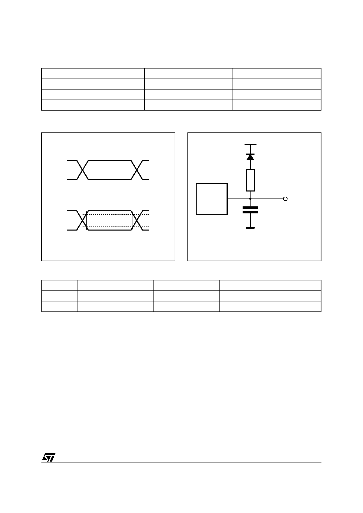
Table6. AC MeasurementConditions
SRAM Interface Levels EPROM Interface Levels
Input Rise and Fall Times ≤ 10ns ≤ 10ns
Input Pulse Voltages 0 to 3V 0.45V to 2.4V
Input and Output Timing Ref. Voltages 1.5V 0.8V and 2V
M28F101
Figure 3. AC TestingInput Output Waveform
SRAM Interface
3V
1.5V
0V
EPROM Interface
2.4V
0.45V
Table 7. Capacitance
Symbol Parameter Test Condition Min Max Unit
C
IN
C
OUT
Note: 1. Sampled only, not 100% test.ed
Input Capacitance VIN=0V 6 pF
Output Capacitance V
(1)
(TA=25°C, f = 1 MHz )
2.0V
0.8V
AI01275
Figure 4. ACTesting Load Circuit
1.3V
1N914
3.3kΩ
DEVICE
UNDER
TEST
CL= 30pF or 100pF
CL= 30pF for SRAM Interface
CL= 100pF for EPROM Interface
CLincludes JIG capacitance
=0V 12 pF
OUT
OUT
AI01276
READ/WRITE MODES (cont’d)
Awritetothecommandregisterismadebybringing
WLowwhileEisLow.ThefallingedgeofW latches
Addresses, while the rising edge latches Data,
which are used for those commands that require
address inputs, command input or provide data
output.
The supply voltage V
canbe applied in any order. When the device
V
PP
is powered up or when V
and the program voltage
CC
is ≤ 6.5V the contents
PP
of the command register defaults to 00h, thus
automaticallysetting-up Read operations. In addition a specific command may be used to set the
commandregister to 00h for reading the memory.
Thesystem designer may chose to provide a constanthigh V
all operations,or toswitchthe V
and use the register commands for
PP
fromlow to high
PP
only when needing to eraseor program the memory. Allcommandregisteraccess isinhibited when
falls below the Erase/Write Lockout Voltage
V
CC
) of 2.5V.
(V
LKO
If the device is deselected during Erasure, Programmingor Verification it will draw active supply
currentsuntil the operations are terminated.
The device is protected against stress caused by
long erase or program times. If the end of Erase or
Programming operations are not terminated by a
Verifycycle within a maximum time permitted, an
internal stop timer automatically stops the operation.The deviceremainsin an inactivestate, ready
to start a Verifyor ResetMode operation.
5/23
Page 6
M28F101
Table8. DC Characteristics
= 0 to 70°C, –40to 85 °C or–40 to 125 °C;VCC=5V±10%)
(T
A
Symbol Parameter TestCondition Min Max Unit
I
I
LO
I
CC
I
CC1
I
CC2
I
CC3
I
CC4
I
CC5
I
LPP
I
PP
I
PP1
I
PP2
I
PP3
I
PP4
V
V
V
V
OH
V
PPL
V
PPH
V
I
ID
V
LKO
Note: 1. Not 100% tested.Characterisation Data available.
Input Leakage Current 0V ≤ VIN≤ V
LI
Output Leakage Current 0V ≤ V
OUT
≤ V
CC
CC
Supply Current (Read) E = VIL, f = 6MHz 30 mA
Supply Current (Standby) TTL E = V
Supply Current (Standby) CMOS E = V
(1)
Supply Current (Programming) DuringProgramming 10 mA
(1)
Supply Current (Program Verify) During Verify 15 mA
(1)
Supply Current (Erase) During Erasure 15 mA
(1)
Supply Current (Erase Verify) During Erase Verify 15 mA
Program Leakage Current VPP≤ V
Program Current (Read or
Standby)
(1)
Program Current (Programming) VPP=V
(1)
Program Current (Program
Verify)
(1)
Program Current (Erase) VPP=V
(1)
Program Current (Erase Verify) VPP=V
Input Low Voltage –0.5 0.8 V
IL
Input High VoltageTTL 2 VCC+ 0.5 V
IH
PPH
V
PP=VPPH
PPH
Input High Voltage CMOS 0.7 V
= 5.8mA (grade 1) 0.45 V
I
Output Low Voltage
OL
Output High Voltage CMOS
Output High Voltage TTL I
OL
I
= 2.1mA (grade 6) 0.45 V
OL
I
OH
I
OH
OH
Program Voltage (Read
Operations)
Program Voltage (Read/Write
Operations)
A9 Voltage (Electronic Signature) 11.5 13 V
ID
(1)
A9 Current (Electronic Signature) A9 = V
Supply Voltage, Erase/Program
Lock-out
IH
± 0.2V 50 µA
CC
CC
V
PP>VCC
V
≤ V
PP
CC
, During Programming 30 mA
, During Verify 5 mA
, During Erase 30 mA
PPH
, During Erase Verify 5 mA
CC
= –100µA 4.1 V
= –2.5mA 0.85 V
CC
= –2.5mA 2.4 V
0 6.5 V
11.4 12.6 V
ID
2.5 V
±1 µA
±10 µA
1mA
±10 µA
120 µA
±10 µA
VCC+ 0.5 V
200 µA
V
6/23
Page 7
Table 9A. Read Only Mode AC Characteristics
= 0 to70 °C, –40 to 85 °C or –40 to125 °C; 0V ≤ VPP≤ 6.5V)
(T
A
Symbol Alt Parameter TestCondition
t
WHGL
t
AVAV
t
AVQV
(1)
t
ELQX
t
ELQV
(1)
t
GLQX
t
GLQV
(1)
t
EHQZ
(1)
t
GHQZ
t
AXQX
Note: 1. Sampled only, not 100% tested
Write Enable High to
Output Enable Low
t
Read Cycle Time E = VIL,G=VIL70 90 100 ns
RC
Address Validto
t
ACC
Output Valid
Chip Enable Low to
t
LZ
Output Transition
Chip Enable Low to
t
CE
Output Valid
Output Enable Low to
t
OLZ
Output Transition
Output Enable Low to
t
OE
Output Valid
Chip Enable High to
Output Hi-Z
Output Enable High to
t
DF
Output Hi-Z
Address Transitionto
t
OH
Output Transition
E=V
G=V
G=V
G=V
E=V
,G=V
IL
E=V
E=V
E=V
,G=V
IL
IL
IL
IL
IL
IL
IL
IL
IL
M28F101
M28F101
-70 -90 -100
=5V±5% VCC=5V±10% VCC=5V±10%
V
CC
SRAM
Interface
EPROM
Interface
EPROM
Interface
Min Max Min Max Min Max
666µs
70 90 100 ns
000ns
70 90 100 ns
000ns
40 40 45 ns
0 30 0 45 0 45 ns
0 30 0 30 0 30 ns
000ns
Unit
Read Mode. The Read Mode is the default at
power up or may be set-up by writing 00h to the
command register. Subsequent read operations
outputdatafromthememory.Thememoryremains
in the Read Mode until a new commandis written
to the command register.
ElectronicSignatureMode. In order to select the
correct erase and programming algorithms for onboard programming, the manufacturerand device
codesmay beread directly. It isnot neccessaryto
apply a high voltage to A9 when using the command register. The Electronic Signature Mode is
set-upby writing 90htothe commandregister.The
following read cycles,with address inputs00000h
or 00001h, output the manufactureror devicetype
codes.The command is terminated by writinganothervalid command to the commandregister(for
exampleReset).
7/23
Page 8

M28F101
Table 9B. Read Only Mode AC Characteristics
=0 to 70 °C, –40 to 85 °C or –40 to 125 °C; 0V ≤ VPP≤ 6.5V)
((T
A
Symbol Alt Parameter Test Condition
t
WHGL
t
AVAV
t
AVQV
(1)
t
ELQX
t
ELQV
(1)
t
GLQX
t
GLQV
(1)
t
EHQZ
(1)
t
GHQZ
t
AXQX
Note: 1. Sampled only, not 100% tested
Write Enable High to
Output Enable Low
t
Read Cycle Time E = VIL,G=VIL120 150 200 ns
RC
Address Validto
t
ACC
Output Valid
Chip Enable Low to
t
LZ
Output Transition
Chip Enable Low to
t
CE
Output Valid
Output Enable Low to
t
OLZ
Output Transition
Output Enable Low to
t
OE
Output Valid
Chip Enable High to
Output Hi-Z
Output Enable High to
t
DF
Output Hi-Z
Address Transitionto
t
OH
Output Transition
E=V
G=V
G=V
G=V
E=V
,G=V
IL
E=V
E=V
E=V
,G=V
IL
IL
IL
IL
IL
IL
IL
IL
IL
M28F101
-120 -150 -200
=5V±10% VCC=5V±10% VCC=5V±10%
V
CC
EPROM
Interface
EPROM
Interface
EPROM
Interface
Unit
Min Max Min Max Min Max
666µs
120 150 200 ns
000ns
120 150 200 ns
000ns
50 55 60 ns
055055060ns
030035040ns
000ns
Erase and Erase Verify Modes. The memory is
erased by first Programming all bytes to 00h, the
Erase command then erases them to FFh. The
Erase Verify command is then used to read the
memory byte-by-byte for a content of FFh. The
Erase Mode is set-up by writing 20h to the command register. The write cycle is then repeated to
start the erase operation. Erasure starts on the
rising edge of W during this secondcycle.Eraseis
followed by an Erase Verify which reads an addressedbyte.
8/23
Erase Verify Mode is set-up by writing A0h to the
commandregisterand at the same time supplying
the address of the byte to be verified. The rising
edgeof W duringthe set-up of the first EraseVerify
Mode stops the Erase operation. The following
read cycle is made with an internally generated
marginvoltageapplied; readingFFh indicatesthat
all bits of the addressed byte are fullyerased.The
whole contentsof the memory are verified by repeating theErase VerifyOperation,first writingthe
set-upcode A0h with the address of the byte to be
verified and then reading the byte contents in a
secondread cycle.
Page 9

Figure5. Read Mode ACWaveforms
A0-A16
E
G
tGLQV
tGLQX
tAVAV
tAVQV tAXQX
tELQV
tELQX
tEHQZ
tGHQZ
M28F101
DQ0-DQ7
Figure6. Read Command Waveforms
V
PP
tVPHEL
A0-A16
E
tELWL tWHEH
G
tGHWL
W
tWLWH
DATA OUT
AI00671
VALID
tAVQV
tELQV tEHQZ
tWHGL
tGLQV
tAXQX
tGHQZ
DQ0-DQ7 DATA OUTCOMMAND
tWHDXtDVWH
READREAD SET-UP
AI00672
9/23
Page 10

M28F101
Figure7. ElectronicSignatureCommand Waveforms
V
PP
tVPHEL
A0-A16
E
tELWL tWHEH
G
tGHWL
W
tWLWH
tWHDXtDVWH
DQ0-DQ7 DATA OUTCOMMAND
READ
ELECTRONIC
SIGNATURE SET-UP
READ/WRITE MODES (cont’d)
As the Erase algorithmflow chartshows,whenthe
data read during Erase Verify is not FFh, another
Eraseoperationis performedand verification continuesfromthe addressofthelastverifiedbyte. The
command is terminated by writing another valid
command to the command register (for example
Programor Reset).
Program and Program Verify Modes. The ProgramModeis set-upbywriting40htothecommand
register. This is followed by a second write cycle
which latches the address and data of the byte to
be programmed.The rising edge of W during this
secind cycle starts the programming operation.
Programmingisfollowedby aProgramVerify ofthe
datawritten.
00000h-00001h
tAVQV
tELQV tEHQZ
tWHGL
tGLQV
READ
MANUFACTURER
OR DEVICE
tAXQX
tGHQZ
AI00673
ProgramVerify Modeisset-upbywritingC0hto the
commandregister. The rising edgeof W duringthe
set-up of the ProgramVerify Mode stops the Programming operation. The following read cycle, of
the address already latched during programming,
is made with an internallygenerated margin voltageapplied,readingvaliddataindicatesthatallbits
havebeen programmed.
ResetMode.Thiscommandis usedto safelyabort
Erase or Program Modes. The Reset Mode is
set-up and performed by writing FFh two times to
the command register. The command should be
followed by writing a valid command to the the
commandregister (for exampleRead).
10/23
Page 11

Table 10A. Read/Write Mode AC Characteristics, W and E Controlled
= 0 to70 °C, –40 to 85 °C or –40 to125 °C)
(T
A
M28F101
-70 -90 -100
Symbol Alt Parameter
t
VPHEL
t
VPHWL
t
WHWH3
t
AVWL
t
AVEL
t
WLAX
t
ELAX
t
ELWL
t
WLEL
t
GHWL
t
GHEL
t
DVWH
t
DVEH
t
WLWH
t
ELEH
t
WHDX
t
EHDX
t
WHWH1
t
EHEH1
t
WHWH2
t
WHEH
t
EHWH
t
WHWLtWPH
t
EHEL
t
WHGL
t
EHGL
t
AVQV
(1)
t
ELQX
t
ELQV
(1)
t
GLQX
t
GLQV
(1)
t
EHQZ
(1)
t
GHQZ
t
AXQX
Note: 1. Sampled only, not 100% tested.
VPPHigh to Chip Enable Low 1 1 1 µs
VPPHigh to Write Enable Low 1 1 1 µs
t
Write Cycle Time 70 90 100 ns
WC
t
Address Validto Write Enable Low 0 0 0 ns
AS
Address Validto Chip Enable Low 0 0 0 ns
t
Write Enable Low to Address Transition 40 40 40 ns
AH
Chip Enable Low to Address Transition 50 60 60 ns
t
Chip Enable Low to Write Enable Low 10 15 15 ns
CS
Write Enable Low to Chip Enable Low 0 0 0 ns
Output Enable High to Write Enable
Low
Output Enable High to ChipEnable Low 0 0 0 µs
t
Input Validto Write Enable High 30 40 40 ns
DS
Input Validto Chip Enable High 30 35 40 ns
Write Enable Low to Write Enable High
t
WP
(Write Pulse)
Chip Enable Low to Chip Enable High
(Write Pulse)
t
Write Enable High to InputTransition 10 10 10 ns
DH
Chip Enable High to Input Transition 10 10 10 ns
Duration of Program Operation 9.5 9.5 9.5 µs
Duration of Program Operation 9.5 9.5 9.5 µs
Duration of Erase Operation 9.5 9.5 9.5 ms
t
Write Enable High to Chip Enable High 0 0 0 ns
CH
Chip Enable High to WriteEnable High 0 0 0 ns
Write Enable High to Write Enable Low 20 20 20 ns
Chip Enable High to Chip Enable Low 20 20 20 ns
Write Enable High to Output Enable
Low
Chip Enable High to Output Enable Low 6 6 6 µs
t
Addess Validto data Output 70 90 100 ns
ACC
t
Chip Enable Low to Output Transition 0 0 0 ns
LZ
t
Chip Enable Low to Output Valid 70 90 100 ns
CE
t
Output Enable Low to OutputTransition 0 0 0 ns
OLZ
t
Output Enable Low to Output Valid 40 40 45 ns
OE
Chip Enable High to Output Hi-Z 30 40 40 ns
t
Output Enable High to Output Hi-Z 30 30 30 ns
DF
t
Address Transitionto Output Transition 0 0 0 ns
OH
=5V±5% VCC=5V±10% VCC=5V±10%
V
CC
SRAM
Interface
EPROM
Interface
Min Max Min Max Min Max
000µs
35 40 40 ns
35 45 45 ns
666µs
M28F101
Unit
EPROM
Interface
11/23
Page 12

M28F101
Table10B. Read/WriteMode AC Characteristics,W and E Controlled
= 0 to 70°C, –40to 85 °C or–40 to 125 °C)
(T
A
M28F101
-120 -150 -200
Symbol Alt Parameter
t
VPHEL
t
VPHWL
t
WHWH3
t
AVWL
t
AVEL
t
WLAX
t
ELAX
t
ELWL
t
WLEL
t
GHWL
t
GHEL
t
DVWH
t
DVEH
t
WLWH
t
ELEH
t
WHDX
t
EHDX
t
WHWH1
t
EHEH1
t
WHWH2
t
WHEH
t
EHWH
t
WHWLtWPH
t
EHEL
t
WHGL
t
EHGL
t
AVQV
(1)
t
ELQX
t
ELQV
(1)
t
GLQX
t
GLQV
(1)
t
EHQZ
(1)
t
GHQZ
t
AXQX
Note: 1. Sampled only,not100% tested.
VPPHigh to Chip Enable Low 1 1 1 µs
VPPHigh to Write Enable Low 1 1 1 µs
t
Write Cycle Time 120 150 200 ns
WC
t
Address Validto Write Enable Low 0 0 0 ns
AS
Address Validto Chip Enable Low 0 0 0 ns
t
Write Enable Low toAddress Transition 60 60 75 ns
AH
Chip Enable Low to Address Transition 80 80 80 ns
t
Chip EnableLow to Write Enable Low 20 20 20 ns
CS
Write Enable Low to Chip Enable Low 0 0 0 ns
Output Enable High to Write Enable
Low
Output Enable High to Chip Enable Low 0 0 0 µs
t
Input Validto Write Enable High 50 50 50 ns
DS
Input Validto Chip Enable High 50 50 50 ns
Write Enable Low to Write Enable High
t
WP
(Write Pulse)
Chip EnableLow to Chip Enable High
(Write Pulse)
t
Write Enable High to Input Transition 10 10 10 ns
DH
Chip Enable High to Input Transition 10 10 10 ns
Duration of Program Operation 9.5 9.5 9.5 µs
Duration of Program Operation 9.5 9.5 9.5 µs
Duration of Erase Operation 9.5 9.5 9.5 ms
t
Write Enable High to Chip Enable High 0 0 0 ns
CH
Chip Enable High to Write Enable High 0 0 0 ns
Write Enable High to Write Enable Low 20 20 20 ns
Chip Enable High to Chip Enable Low 20 20 20 ns
Write Enable High to Output Enable
Low
Chip Enable High to Output Enable Low 6 6 6 µs
t
Addess Validto data Output 120 150 200 ns
ACC
t
Chip EnableLow to Output Transition 0 0 0 ns
LZ
t
Chip EnableLow to Output Valid 120 150 200 ns
CE
t
Output Enable Low to Output Transition 0 0 0 ns
OLZ
t
Output Enable Low to Output Valid 50 55 60 ns
OE
Chip Enable High to Output Hi-Z 50 55 60 ns
t
Output Enable High to Output Hi-Z 30 35 40 ns
DF
t
Address Transitionto Output Transition 0 0 0 ns
OH
=5V±10% VCC=5V±10% VCC=5V±10%
V
CC
EPROM
Interface
Interface
Min Max Min Max Min Max
000µs
60 60 60 ns
70 70 70 ns
666µs
EPROM
Unit
EPROM
Interface
12/23
Page 13

Figure8. Erase Set-up and Erase VerifyCommandsWaveforms, W Controlled
M28F101
ERASE OPERATION
VALID
tWLAX
tAVWL
tELQV tEHQZ
tWHEH
tELWL
tGHQZtWHWH2
tWHGLtWHWL
tWLWH tGLQV
tWHDXtDVWH
DATA OUT
VERIFY
COMMAND
ERASE VERIFY
AI00674
READ
SET-UP
COMMAND
ERASE SET-UP
tWHWH3
tVPHEL
G
tGHWL
W
tELWL tWHEH
PP
V
A0-A16
E
tWHDXtDVWH
tWLWH
DQ0-DQ7 COMMAND
(REPEAT OF 1st CYCLE)
ERASE SET-UP
13/23
Page 14

M28F101
Figure9. Erase Set-up and Erase VerifyCommandsWaveforms, E Controlled
ERASE OPERATION
VALID
tELAX
tAVEL
tGLQV
tEHWH
tWLEL
tGHQZtEHEH2
tEHGLtEHEL
tEHQZ
tELEH tELQV
tEHDXtDVEH
DATA OUT
VERIFY
COMMAND
ERASE VERIFY
AI01313
READ
SET-UP
14/23
V
PP
tVPHWL
A0-A16
tWHWH3
W
tWLEL tEHWH
COMMAND
ERASE SET-UP
tEHDXtDVEH
tELEH
tGHEL
G
E
DQ0-DQ7 COMMAND
(REPEAT OF 1st CYCLE)
ERASE SET-UP
Page 15

Figure10. ProgramSet-up and ProgramVerify Commands Waveforms,W Controlled
M28F101
PROGRAM OPERATION
tELQV tEHQZ
tWHEH
tGHQZ
tWHGLtWHWL
tWHWH1
tELWL
tWLWH tGLQV
tWHDXtDVWH
tWHDX
DATA OUT
VERIFY
COMMAND
PROGRAM
AI00675
READ
VERIFY SET-UP
V
PP
tVPHEL
VALID
A0-A16
tWLAX
tWHWH3
tAVWL
E
tWHEH
tELWL tWHEH
G
tELWL
tGHWL
W
tWLWH
tWHDX
tWLWH
tDVWH
tDVWH
DATA IN
ADDRESS AND
PROGRAM SET-UP
DQ0-DQ7 COMMAND
DATA LATCH
15/23
Page 16

M28F101
Figure11. ProgramSet-up and Program Verify Commands Waveforms, E Controlled
PROGRAM OPERATION
tELAX
tGLQV
tEHWH
tGHQZ
tEHGLtEHEL
tEHEH1
tWLEL
tELQV tEHQZ
tELEH
tELEH
tEHDXtDVEH
tEHDX
DATA OUT
VERIFY
COMMAND
PROGRAM
DATA IN
AI00676
READ
VERIFY SET-UP
16/23
V
PP
tVPHEL
VALID
A0-A16
tWHWH3
tAVEL
W
tEHWH
tWLEL tEHWH
DATA LATCH
tDVEH
tEHDX
tWLEL
tDVEH
tELEH
tGHEL
G
E
ADDRESS AND
PROGRAM SET-UP
DQ0-DQ7 COMMAND
Page 17

M28F101
Figure12. Erasing Flowchart
VPP= 12V
PROGRAM
BYTES TO 00h
n=0, Addr=00000h
ERASE SET-UP
Wait 10ms
ERASE VERIFY
Latch Addr.
Wait 6µs
READ DATA OUTPUT
Data
NO
OK
YES
Last
Addr
YES
READ COMMAND
VPP< 6.5V, PASS
VPP<
FAIL
YES
NO
++n
LIMIT
6.5V
ALL
NO
Addr++
AI00678
Figure13. ProgrammingFlowchart
VPP= 12V
n=0
PROGRAM SET-UP
Latch Addr, Data
Wait 10µs
PROGRAM VERIFY
++n
READ DATA OUTPUT
NO
READ COMMAND
VPP< 6.5V, PASS
Wait 6µs
Data
OK
YES
Last
Addr
YES
NO
VPP<
FAIL
NO
YES
=25
6.5V
Addr++
AI00677
Limit: 1000 at grade 1; 6000 at grades 3 &6.
PRESTOF ERASE ALGORITHM
The PRESTO F Erase Algorithm guarantees that
the device will be erased in a reliable way. The
algorithmfirst programmsall bytes to 00h in order
to ensure uniform erasure. The programming follows the PRESTO F Programming Algorithm.
Erase is set-up by writing 20h to the command
register, the erasure is started by repeating this
writecycle. EraseVerifyis set-upby writingA0h to
the command registertogetherwith theaddress of
the byte to be verified. The subsequent read cycle
reads the data which is compared to FFh. Erase
Verify begins at address 0000h and continues to
the last addressoruntilthe comparisonof the data
to 0FFhfails. If this occurs, the addressof the last
byte checked is stored and a new Erase operation
performed. Erase Verify then continues from the
address of the stored location.
PRESTOF PROGRAMALGORITHM
ThePRESTO F ProgrammingAlgorithm applies a
series of 10µs programmingpulses to a byte until
a correct verify occurs. Up to 25 programming
operations are allowed for one byte. Program is
set-upby writing 40h to the command register, the
programming is started after the next write cycle
which also latches the address and data to be
programmed. Program Verify is set-up by writing
C0h to the command register, followed by a read
cycle and a compare of the data read to the data
expected.During Program and ProgramVerify operations a MARGIN MODE circuit is activated to
guaranteethatthecellis programmedwitha safety
margin.
17/23
Page 18

M28F101
ORDERING INFORMATION SCHEME
Example: M28F101 -70 X N 1 TR
Operating Voltage
F5V
Speed
-70 70ns
-90 90ns
-100 100ns
-120 120ns
-150 150ns
-200 200ns
Power Supplies
blank V
XV
± 10%
CC
± 5%
CC
Package
P PDIP32
K PLCC32
N TSOP32
8 x 20mm
Devicesare shippedfrom the factorywith the memory content erased (toFFh).
Option
R Reverse Pinout
TR Tape& Reel
Packing
Temp.Range
1 0 to 70 °C
3 –40 to 125 °C
6 –40 to 85 °C
For a listof availableoptions(Speed,Package,etc...)orfor furtherinformationon anyaspectofthisdevice,
please contact the SGS-THOMSON Sales Officenearest to you.
18/23
Page 19

PDIP32 - 32 pin Plastic DIP, 600 mils width
M28F101
Symb
Typ Min Max Typ Min Max
A 4.83 0.190
A1 0.38 – 0.015 –
A2––––––
B 0.41 0.51 0.016 0.020
B1 1.14 1.40 0.045 0.055
C 0.20 0.30 0.008 0.012
D 41.78 42.04 1.645 1.655
E 15.24 15.88 0.600 0.625
E1 13.46 13.97 0.530 0.550
e1 2.54 – – 0.100 – –
eA 15.24 – – 0.600 – –
L 3.18 3.43 0.125 0.135
S 1.78 2.03 0.070 0.080
α 0° 15° 0° 15°
N32 32
PDIP32
mm inches
Drawing is not to scale.
B1 B e1
D
S
N
1
A2A1A
L
Cα
eA
E1 E
PDIP
19/23
Page 20

M28F101
PLCC32 - 32 lead Plastic Leaded Chip Carrier,rectangular
Symb
Typ Min Max Typ Min Max
A 2.54 3.56 0.100 0.140
A1 1.52 2.41 0.060 0.095
B 0.33 0.53 0.013 0.021
B1 0.66 0.81 0.026 0.032
D 12.32 12.57 0.485 0.495
D1 11.35 11.56 0.447 0.455
D2 9.91 10.92 0.390 0.430
E 14.86 15.11 0.585 0.595
E1 13.89 14.10 0.547 0.555
E2 12.45 13.46 0.490 0.530
e 1.27 – – 0.050 – –
N32 32
Nd 7 7
Ne 9 9
CP 0.10 0.004
PLCC32
mm inches
Ne E1 E
Drawing is not to scale.
20/23
PLCC
D
D1
1N
Nd
D2/E2
A1
B1
e
B
A
CP
Page 21

M28F101
TSOP32 Normal Pinout - 32 lead Plastic Thin Small Outline, 8 x 20mm
Symb
Typ Min Max Typ Min Max
A 1.04 1.24 0.041 0.049
A1 0.05 0.20 0.002 0.008
A2 0.95 1.06 0.037 0.042
B 0.15 0.27 0.006 0.011
C 0.10 0.21 0.004 0.008
D 19.90 20.12 0.783 0.792
D1 18.24 18.49 0.718 0.728
E 7.90 8.10 0.311 0.319
e 0.50 – – 0.020 – –
L 0.30 0.70 0.012 0.028
α 0° 5° 0° 5°
N32 32
CP 0.10 0.004
TSOP32
mm inches
Drawing is not to scale.
1N
E
N/2
D1
D
DIE
TSOP-a
A2
e
B
A
CP
C
LA1 α
21/23
Page 22

M28F101
TSOP32 Reverse Pinout - 32 lead Plastic Thin Small Outline, 8 x 20mm
Symb
Typ Min Max Typ Min Max
A 1.04 1.24 0.041 0.049
A1 0.05 0.20 0.002 0.008
A2 0.95 1.06 0.037 0.042
B 0.15 0.27 0.006 0.011
C 0.10 0.21 0.004 0.008
D 19.90 20.12 0.783 0.792
D1 18.24 18.49 0.718 0.728
E 7.90 8.10 0.311 0.319
e 0.50 – – 0.020 – –
L 0.30 0.70 0.012 0.028
α 0° 5° 0° 5°
N32 32
CP 0.10 0.004
TSOP32
mm inches
Drawing is not to scale.
1N
E
N/2
D1
D
DIE
TSOP-b
A2
e
B
A
CP
C
LA1 α
22/23
Page 23

M28F101
Information furnished is believed to be accurate and reliable.However, SGS-THOMSON Microelectronics assumes no responsibility for the
consequences of use of such informationnor for any infringementof patents or other rights ofthird parties which may result from its use.No
license is granted by implication or otherwise under any patent or patent rights of SGS-THOMSON Microelectronics. Specificationsmentioned
in this publication are subject to change without notice. This publication supersedes and replaces all information previously supplied.
SGS-THOMSON Microelectronics products are not authorized for use as critical componentsin life supportdevices or systemswithout express
written approval of SGS-THOMSON Microelectronics.
1997 SGS-THOMSON Microelectronics - All Rights Reserved
Australia - Brazil - Canada- China - France - Germany - Hong Kong - Italy -Japan - Korea- Malaysia -Malta - Morocco - The Netherlands -
Singapore- Spain - Sweden - Switzerland - Taiwan- Thailand - United Kingdom- U.S.A.
SGS-THOMSON Microelectronics GROUP OF COMPANIES
23/23
 Loading...