

Page 1
1/24June 2000
M28C64
64 Kbit (8K x 8) Parallel EEPROM
With Software Data Protection
■ Fast Access Time:
–90nsatVCC=5 V forM28C64 andM28C64-A
– 120 ns at VCC=3 V for M28C64-xxW
■ Single Supply Voltage:
– 4.5 V to 5.5V for M28C64 and M28C64-A
– 2.7 V to 3.6V for M28C64-xxW
■ Low Power Consumption
■ Fast BYTE and PAGE WRITE (up to 64 Bytes)
– 1 ms at VCC=4.5 V for M28C64-A
– 3 ms at VCC=4.5 V for M28C64
– 5 ms at VCC=2.7 V for M28C64-xxW
■ Enhanced Write Detection and Monitoring:
– Ready/Busy Open DrainOutput
– Data Polling
– Toggle Bit
– Page Load Timer Status
■ JEDEC Approved Bytewide Pin-Out
■ Software Data Protection
■ 100000 Erase/Write Cycles (minimum)
■ Data Retention (minimum):
– 40 Years for M28C64 and M28C64-xxW
– 10 Years for M28C64-A
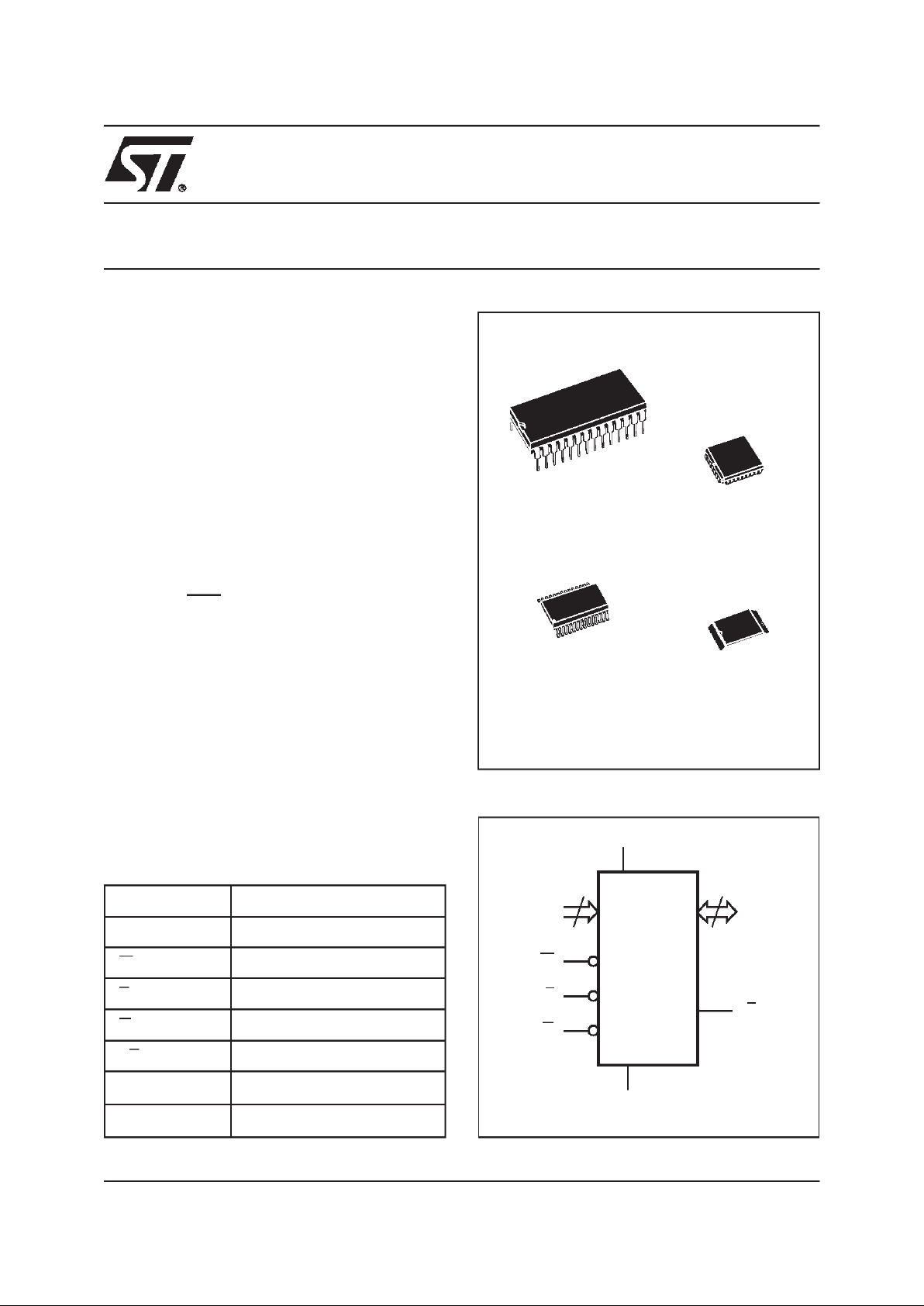
Figure 1. Logic Diagram
AI01350C
13
A0-A12
W
DQ0-DQ7
V
CC
M28C64
G
E
V
SS
8
RB
Table 1. Signal Names
A0-A12 Address Input
DQ0-DQ7 Data Input / Output
W Write Enable
E Chip Enable
G Output Enable
RB Ready / Busy
V
CC
Supply Voltage
V
SS
Ground
PDIP28 (BS)
SO28 (MS)
300 mil width
PLCC32 (KA)
28
1
TSOP28 (NS)
8 x 13.4 mm
28
1
Page 2
M28C64
2/24
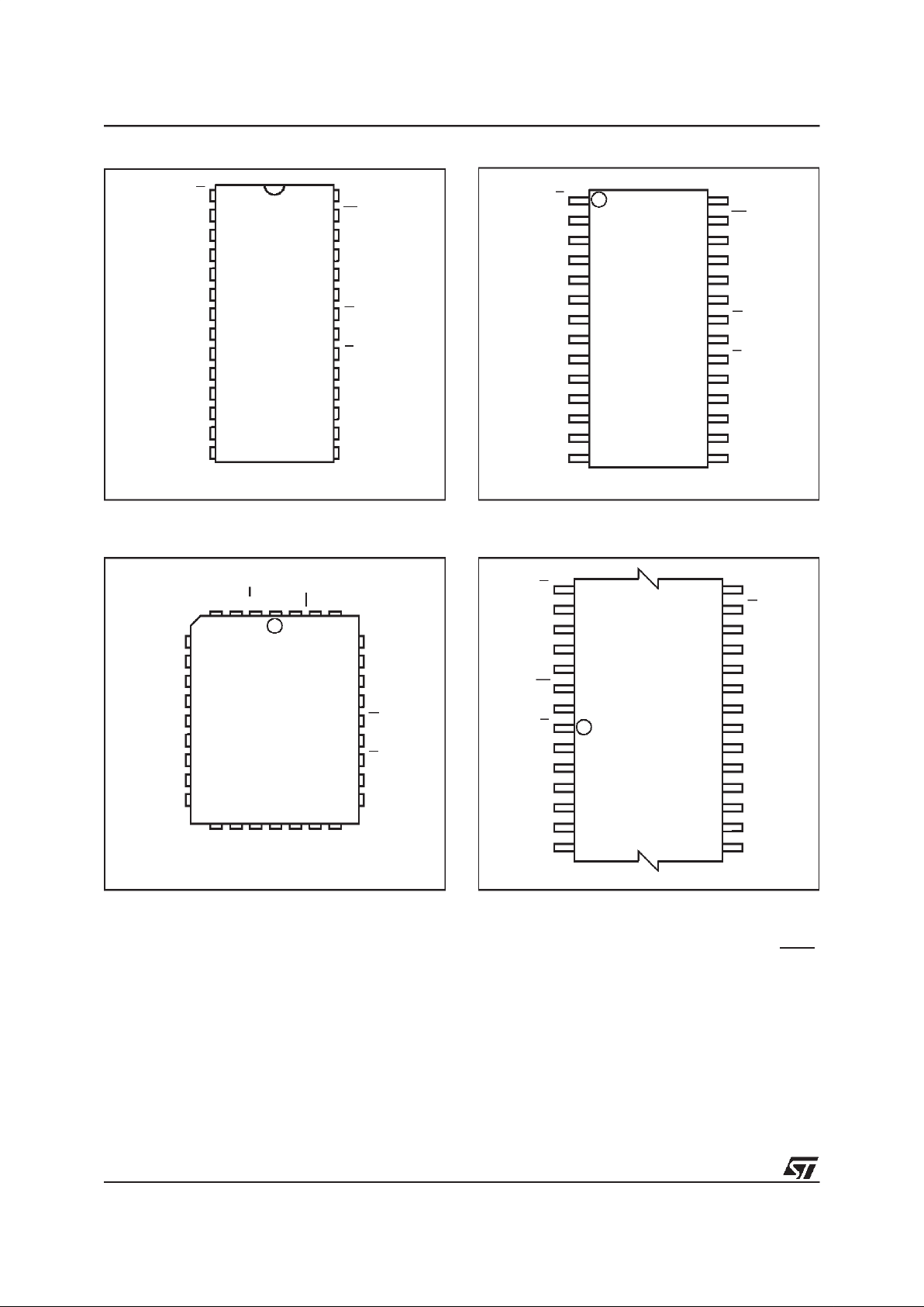
Figure 2A. DIP Connections
Note: 1. NC = Not Connected
Figure 2B. PLLC Connections
Note: 1. NC = Not Connected
2. DU = Do Not Use
A1
A0
DQ0
A7
A4
A3
A2
A6
A5
NC
A10
A8
A9
DQ7
W
A11
G
E
DQ5DQ1
DQ2
DQ3V
SS
DQ4
DQ6
A12
RB V
CC
AI01351C
M28C64
8
1
2
3
4
5
6
7
9
10
11
12
13
14
16
15
28
27
26
25
24
23
22
21
20
19
18
17
AI01352D
NC
A8
A10
DQ4
17
A0
NC
DQ0
DQ1
DQ2
DU
DQ3
A6
A3
A2
A1
A5
A4
9
W
A9
1
RB
A11
DQ6
A7
DQ7
32
DU
V
CC
M28C64
A12
NC
DQ5
G
E
25
V
SS
Figure 2C. SO Connections
Note: 1. NC =Not Connected
Figure 2D. TSOP Connections
Note: 1. NC =Not Connected
DQ0
DQ1
A3
A0
A2
A1
A10
E
NC
DQ7
G
DQ5
V
CC
DQ4
A9
W
A4
RB
A7
AI01353C
M28C64
8
2
3
4
5
6
7
9
10
11
12
13
14
22
21
20
19
18
17
16
15
DQ2
V
SS
A6
A5
DQ6
28
27
26
25
24
23 A11
DQ3
1
A12
A8
A1
A0
DQ0
A5
A2
A4
A3
A9
A11
DQ7
A8
G
E
DQ5
DQ1
DQ2
DQ3
DQ4
DQ6
NC
W
A12
A6
RB
V
CC
A7
AI01354C
M28C64
28
1
22
78
14
15
21
V
SS
A10
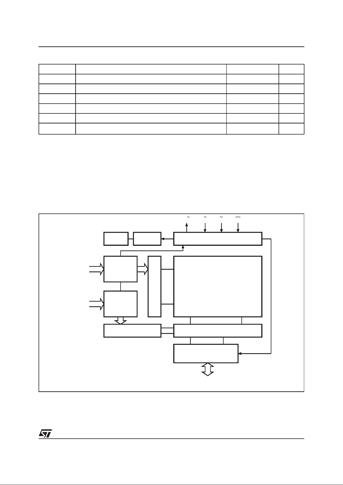
DESCRIPTION
The M28C64 devices consist of 8192x8 bits of low
power, parallel EEPROM, fabricated with
STMicroelectronics’ proprietary single polysilicon
CMOS technology. The devices offer fast access
time, with low power dissipation, and require a
single voltage supply (5V or 3V, depending on the
option chosen).
The device has been designed to offer a flexible
microcontroller interface, featuring both hardware
and software handshaking, with Ready/Busy,
Data Polling and Toggle Bit. The device supports
a 64 byte Page Write operation. Software Data
Protection (SDP) is also supported, using the
standard JEDEC algorithm.
Page 3
3/24
M28C64
Figure 3. Block Diagram
AI01355
ADDRESS
LATCH
A6-A12
(Page Address)
X DECODE
CONTROL LOGIC
64K ARRAY
ADDRESS
LATCH
A0-A5
Y DECODE
VPPGEN RESET
SENSE AND DATA LATCH
I/O BUFFERS
RB E G W
PAGE
LOAD
TIMER STATUS
TOGGLE BIT
DATA POLLING
DQ0-DQ7
Table 2. Absolute Maximum Ratings
1
Note: 1. Except for the rating “Operating Temperature Range”, stresses above those listed in the Table “Absolute Maximum Ratings” may
cause permanent damage to the device. These arestress ratings only, and operation of the device at these or any other conditions
above those indicated in the Operating sections of this specification is not implied. Exposure to Absolute Maximum Rating conditions for extended periods may affect device reliability. Refer also to the ST SURE Program and other relevant quality documents.
2. MIL-STD-883C, 3015.7 (100 pF, 1500 Ω)
Symbol Parameter Value Unit
T
A
Ambient Operating Temperature -40 to 125 °C
T
STG
Storage Temperature -65 to 150 °C
V
CC
Supply Voltage -0.3 to VCC+1 V
V
IO
Input or Output Voltage
-0.6 to V
CC
+0.6
V
V
I
Input Voltage -0.3 to 6.5 V
V
ESD Electrostatic Discharge Voltage (Human Body model)
2
4000 V
Page 4
M28C64
4/24
Table 3. Operating Modes
1
Note: 1. 0=VIL;1=VIH;X=V
IH
or V
IL
; V=12V ± 5%.
Mode E G W DQ0-DQ7
Stand-by 1 X X Hi-Z
Output Disable X 1 X Hi-Z
Write Disable X X 1 Hi-Z
Read 0 0 1 Data Out
Write 0 1 0 Data In
Chip Erase 0 V 0 Hi-Z
SIGNAL DESCRIPTION
The external connections to the device are
summarized in Table 1,and their use in Table 3.
Addresses (A0-A12). The address inputs are
used to select one byte from the memory array
during a read or write operation.
Data In/Out (DQ0-DQ7). The contents of the data
byte arewritten to,or read from,the memory array
through the Data I/O pins.
Chip Enable (E). The chip enable input must be
held low to enable read and write operations.
When Chip Enable is high, power consumption is
reduced.
Output Enable (G). The Output Enable input
controls the data output buffers, and is used to
initiate read operations.
Write Enable(W). TheWrite Enable input controls
whether the addressed locationis to be read, from
or written to.
Ready/Busy (RB). Ready/Busy is an open drain
output that can be used to detect the end of the
internal write cycle.
DEVICE OPERATION
In order to prevent datacorruption and inadvertent
write operations, an internal VCCcomparator
inhibits the Write operations if the VCCvoltage is
lowerthan VWI(see Table 4A and Table4B). Once
the voltage applied on the VCCpin goes over the
VWIthreshold (VCC>VWI), write access to the
memory is allowed after a time-out t
PUW
,as
specified in Table 4A and Table 4B.
Further protection against data corruption is
offered by the E and W low pass filters: any glitch,
on the E and W inputs, witha pulsewidth less than
10 ns (typical) is internally filtered out to prevent
inadvertent write operations to the memory.
Table 4A. Power-Up Timing1for M28C64 (5V range)
(TA= 0 to70 °C or –40 to 85 °C or –40 to 125 °C; VCC= 4.5 to 5.5 V)
Note: 1. Sampled only, not 100% tested.
Table 4B. Power-Up Timing1for M28C64-xxW (3V range)
(TA= 0 to70 °C or –40 to 85 °C; VCC= 2.7 to 3.6 V)
Note: 1. Sampled only, not 100% tested.
Symbol Parameter Min. Max. Unit
t
PUR
Time Delay to Read Operation 1 µs
t
PUW
Time Delay to Write Operation (once VCC≥ VWI)10ms
V
WI
Write Inhibit Threshold 3.0 4.2 V
Symbol Parameter Min. Max. Unit
t
PUR
Time Delay to Read Operation 1 µs
t
PUW
Time Delay to Write Operation (once VCC≥ VWI)15ms
V
WI
Write Inhibit Threshold 1.5 2.5 V
Page 5
5/24
M28C64
Read
The deviceis accessed like a static RAM. When E
and G are low, and W is high, the contents of the
addressed location are presented on the I/O pins.
Otherwise, when either G or Eis high,the I/Opins
revert to their high impedance state.
Write
Write operations are initiated when both W and E
are low and G is high. The device supports both
W-controlled and E-controlled write cycles (as
shown in Figure 11 and Figure12). The address is
latched during the falling edge of W or E (which
ever occurs later) and the data is latched on the
rising edge of W or E (which ever occurs first).
After a delay, t
WLQ5H
, that cannot be shorter than
the value specified in Table 10Ato Table 10C, the
internal write cycle starts. It continues, under
internal timing control, until the write operation is
complete. The commencement of this period can
be detected by reading the Page Load Timer
Status on DQ5. The end of the cycle can be
detected by reading the status of the Data Polling
and the Toggle Bit functions on DQ7 and DQ6.
Page Write
The Page Write mode allows up to 64 bytes to be
written on a single page in a single go. This is
achieved through a series of successive Write
operations, notwoof which are separatedbymore
than the t
WLQ5H
value (as specified in Table 10A
to Table 10C).
All bytes must be located on the same page
address (A12-A6 must be the same for all bytes).
The internal write cycle can start at any instant
after t
WLQ5H
. Once initiated, the write operation is
internally timed, and continues, uninterrupted,
until completion.
As with the single byte Write operation, described
above, the DQ5, DQ6 and DQ7 lines can be used
to detect the beginning and end of the internally
controlled phase of the Page Write cycle.
Software Data Protection (SDP)
The device offers a software-controlled writeprotection mechanism that allows the user to
inhibit all write operations to the device. This can
be useful for protecting the memory from
inadvertent write cycles that may occur during
periods of instability (uncontrolled bus conditions
when excessive noise is detected,or when power
supply levels are outside their specified values).
By default, the device is shipped in the
“unprotected” state: the memory contents can be
freely changed by the user. Once the Software
Data Protection Mode is enabled, all write
commands are ignored,and have no effecton the
memory contents.
The device remains in this mode until a valid
Software Data Protection disable sequence is
received. The device reverts to its “unprotected”
state.
The status of the Software Data Protection
(enabled or disabled) is represented by a non-
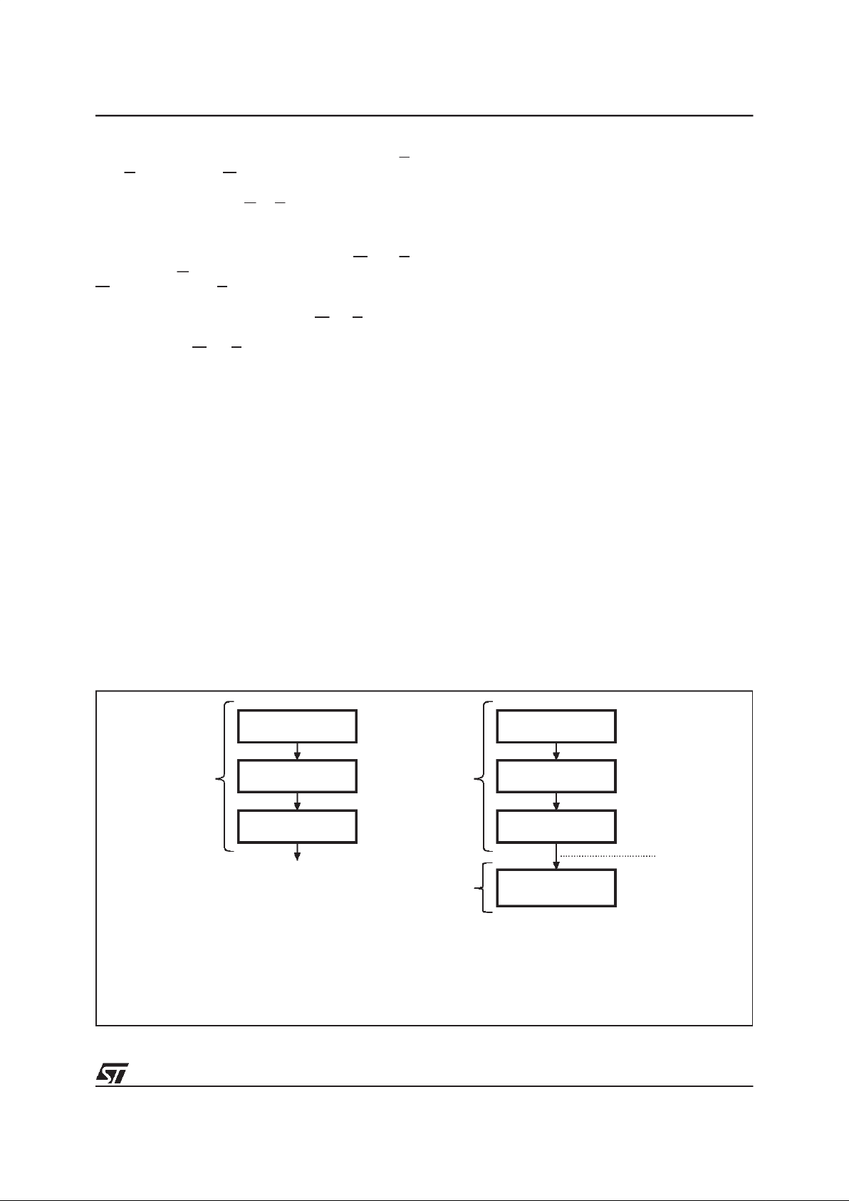
Figure 4. Software Data Protection Enable Algorithm and Memory Write
Note: 1. The most significant address bits (A12 to A6) differ during these specific Page Write operations.
AI01356C
Write AAh in
Address 1555h
Write 55h in
Address 0AAAh
Write A0h in
Address 1555h
SDP is set
Write AAh in
Address 1555h
Write 55h in
Address 0AAAh
Write A0h in
Address 1555h
Page Write
(1 up to 64 bytes)
Write to
Memory
When SDP is SET
SDP Enable Algorithm
Page Write
Timing
(see note 1)
Page Write
Timing
(see note 1)
Write
is enabled
Physical
Page Write
Instruction
Page 6
M28C64
6/24
volatile latch, and is remembered across periods
of the power being off.
The Software Data Protection Enable command
consists of the writing of three specific data bytes
to three specific memory locations (each location
being on a different page), as shown in Figure 4.
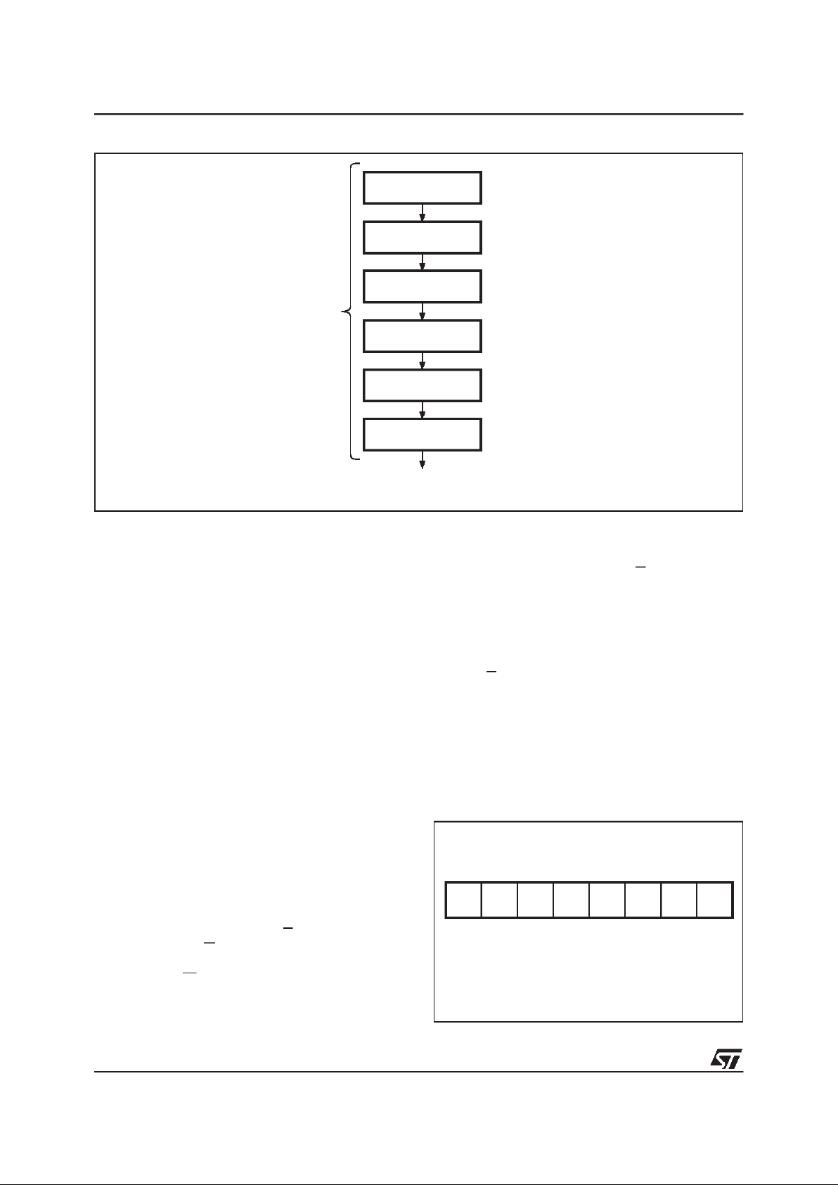
Similarly to disable the Software Data Protection,
the user has to write specific data bytes into six
different locations, as shown in Figure 5. This
complex series of operations protects against the
chance of inadvertent enabling or disabling of the
Software Data Protection mechanism.
When SDP is enabled, the memoryarray can still
have data written to it, but the sequence is more
complex (and hence better protected from
inadvertent use). The sequence is as shown in
Figure 4. This consists of anunlock key, to enable
the write action, at the end of which the SDP
continues to be enabled. This allows the SDP to
be enabled, and data to be written, within a single
Write cycle (tWC).
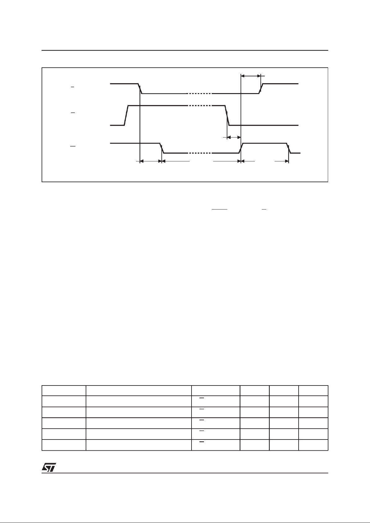
Software Chip Erase
Using this function, available on the M28C64 but
not on the M28C64-A or M28C64-xxW, the
contents of the entire memory are erased (set to
FFh) by holding Chip Enable (E) low, and holding
Output Enable (G) at VCC+7.0V. The chip is
cleared when a 10 ms low pulse is applied to the
Write Enable (W) signal (seeFigure 7 and Table 5
for details).
Status Bits
The devices provide three status bits (DQ7, DQ6
and DQ5), and one output pin (RB), foruse during
write operations. These allow the application to
use the write time latency of the device for getting
on with other work. These signals areavailable on
the I/O port bits DQ7, DQ6 and DQ5 (but only
during programming cycle, once a byte or more
has been latched into the memory)or continuously
on the RB output pin.
Data Polling bit (DQ7). Theinternally timed write
cycle starts after t
WLQ5H
(defined in Table 10A to
Table 10C) has elapsed since the previous byte
was latched in to the memory. The value of the
DQ7 bit of this last byte, is used as a signal
Figure 5. Software Data Protection Disable Algorithm
AI01357B
Write AAhin
Address 1555h
Write 55h in
Address 0AAAh
Write 80h in
Address 1555h
Unprotected State
Write AAhin
Address 1555h
Write 55h in
Address 0AAAh
Write 20h in
Address 1555h
Page Write
Timing
Figure 6. Status Bit Assignment
AI02815
DP TB PLTS Hi-Z Hi-Z Hi-Z Hi-Z Hi-Z
DP
TB
PLTS
Hi-Z
DQ7 DQ6 DQ5 DQ4 DQ3 DQ2 DQ1 DQ0
= Data
Polling
= Toggle Bit
= Page Load Timer
Status
= High impedance
Page 7
7/24
M28C64
Table 5. Chip Erase AC Characteristics1for M28C64 and M28C64-xxW
(TA= 0 to70 °C or –40 to 85 °C or –40 to 125 °C; VCC= 4.5 to 5.5 V)
(TA= 0 to 70 °C or –40 to 85 °C; VCC= 2.7 to 3.6 V)
Note: 1. Sampled only, not 100% tested.
Symbol Parameter Test Condition Min. Max. Unit
t
ELWL
Chip Enable Low to Write Enable Low
G=V
CC
+7V
1 µs
t
WHEH
Write Enable High to Chip Enable High G = VCC+7V 0 ns
t
WLWH2
Write Enable Low to Write Enable High
G=V
CC
+7V
10 ms
t
GLWH
Output Enable Low to Write Enable High
G=V
CC
+7V
1 µs
t
WHRH
Write Enable High to WriteEnable Low G = VCC+7V 3 ms
throughout this write operation: it is inverted while
the internal write operation is underway, and is
inverted back to its original value once the
operation is complete.
Toggle bit (DQ6). The device offers another way
for determining when the internal write cycle is
completed. During the internal Erase/Write cycle,
DQ6 toggles from ’0’ to ’1’ and ’1’ to ’0’ (the first
read value being ’0’) on subsequent attempts to
read any byte of the memory. When the internal
write cycle is complete, the toggling is stopped,
and the valuesread on DQ7-DQ0are those ofthe
addressed memory byte. This indicates that the
device is again available for new Read and Write
operations.
Page Load Timer Status bit (DQ5). An internal
timer is used to measure the period between
successive Write operations, up to t
WLQ5H
(defined in Table 10Ato Table 10C). The DQ5 line
is held low to show when this timer is running
(hence showing that the device has received one
write operation, and is waiting for the next). The
DQ5 line is held high when the counter has
overflowed (hence showingthat the device is now
starting the internal write to the memory array).
Ready/Busy pin. The RB pin is an open drain
output that isheld low duringthe erase/write cycle,
and that is released (allowed to float) at the
completion of the programming cycle.
Figure 7. Chip Erase AC Waveforms (M28C64 and M28C64-xxW)
AI01484B
E
G
W
tWLWH2tELWL
tGLWH
tWHRH
tWHEH
Page 8
M28C64
8/24
Table 6A. Read Mode DC Characteristics for M28C64 and M28C64-A (5V range)
(TA= 0 to70 °C or –40 to 85 °C or –40 to 125 °C; VCC= 4.5 to 5.5 V)
Note: 1. All inputs and outputs open circuit.
Table 6B. Read Mode DC Characteristics for M28C64-xxW (3V range)
(TA= 0 to70 °C or –40 to 85 °C; VCC= 2.7 to 3.6 V)
Note: 1. All inputs and outputs open circuit.
Symbol Parameter Test Condition Min. Max. Unit
I
LI
Input Leakage Current 0 V ≤ VIN≤ V
CC
10 µA
I
LO
Output Leakage Current 0 V ≤ V
OUT
≤ V
CC
10 µA
I
CC
1
Supply Current (TTL inputs) E = VIL,G=VIL, f = 5 MHz 30 mA
Supply Current (CMOS inputs)
E=V
IL
,G=VIL, f = 5 MHz
25 mA
I
CC1
1
Supply Current (Stand-by) TTL
E=V
IH
1mA
I
CC2
1
Supply Current (Stand-by) CMOS E > VCC- 0.3V 100 µA
V
IL
Input Low Voltage -0.3 0.8 V
V
IH
Input High Voltage 2
V
CC
+ 0.5
V
V
OL
Output Low Voltage
I
OL
= 2.1 mA
0.4 V
V
OH
Output High Voltage IOH= -400 µA 2.4 V
Symbol Parameter Test Condition Min. Max. Unit
I
LI
Input Leakage Current
0V≤ V
IN
≤ V
CC
10 µA
I
LO
Output Leakage Current 0 V ≤ V
OUT
≤ V
CC
10 µA
I
CC
1
Supply Current (CMOS inputs)
E=V
IL
,G=VIL, f = 5 MHz, VCC= 3.3V 8 mA
E=V
IL
,G=VIL, f = 5 MHz, VCC= 3.6V 10 mA
I
CC2
1
Supply Current (Stand-by) CMOS E > VCC- 0.3V 20 µA
V
IL
Input Low Voltage -0.3 0.6 V
V
IH
Input High Voltage 2
V
CC
+ 0.5
V
V
OL
Output Low Voltage IOL= 1.6 mA 0.2 V
CC
V
V
OH
Output High Voltage IOH= -400 µA 0.8 V
CC
V
Page 9

9/24
M28C64
Table 7. Input and Output Parameters1(TA=25°C, f = 1 MHz)
Note: 1. Sampled only, not 100% tested.
Table 8. AC Measurement Conditions
Symbol Parameter Test Condition Min. Max. Unit
C
IN
Input Capacitance VIN=0V 6 pF
C
OUT
Output Capacitance V
OUT
=0V 12 pF
Input Rise and Fall Times ≤ 20 ns
Input Pulse Voltages (M28C64, M28C64-A) 0.4 V to 2.4 V
Input Pulse Voltages (M28C64-xxW)
0 V to V
CC
-0.3V
Input and Output Timing Reference Voltages (M28C64, M28C64-A) 0.8 V to 2.0 V
Input and Output Timing Reference Voltages (M28C64-xxW) 0.5 V
CC
Figure 8. AC Testing Input Output Waveforms
AI02101B
4.5V to 5.5V Operating Voltage
2.7V to 3.6V Operating Voltage
VCC– 0.3V
0V
0.5 V
CC
2.4V
0.4V
2.0V
0.8V
Figure 9. AC Testing Equivalent Load Circuit
AI02102B
OUT
CL= 100pF
CLincludes JIG capacitance
I
OL
DEVICE
UNDER
TEST
I
OH
Page 10

M28C64
10/24
Table 9A. Read Mode AC Characteristics for M28C64 and M28C64-A (5V range)
(TA= 0 to70 °C or –40 to 85 °C; VCC= 4.5 to 5.5 V)
Note: 1. Output Hi-Z is defined as the point at which data is no longer driven.
Table 9B. Read Mode AC Characteristics for M28C64 (5V range)
(TA= –40 to 125 °C; VCC= 4.5 to 5.5 V)
Note: 1. Output Hi-Z is defined as the point at which data is no longer driven.
Symbol Alt. Parameter
Test
Condit
ion
M28C64
Unit-90 -12 -15
Min Max Min Max Min Max
t
AVQVtACC
Address Valid to Output Valid
E=V
IL
,
G=V
IL
90 120 150 ns
t
ELQV
t
CE
Chip Enable Low to Output Valid
G=V
IL
90 120 150 ns
t
GLQV
t
OE
Output Enable Low to Output Valid E = V
IL
40 45 50 ns
t
EHQZ
1
t
DF
Chip Enable High to Output Hi-Z G = V
IL
040045050ns
t
GHQZ
1
t
DF
Output Enable High to Output Hi-Z
E=V
IL
040045050ns
t
AXQXtOH
Address Transitionto Output
Transition
E=V
IL
,
G=V
IL
000ns
Symbol Alt. Parameter
Test
Condit
ion
M28C64
Unit-12
Min Max
t
AVQVtACC
Address Valid to Output Valid
E=V
IL
,
G=V
IL
120 ns
t
ELQV
t
CE
Chip Enable Low to Output Valid
G=V
IL
120 ns
t
GLQV
t
OE
Output Enable Low to Output Valid
E=V
IL
45 ns
t
EHQZ
1
t
DF
Chip Enable High to Output Hi-Z
G=V
IL
065ns
t
GHQZ
1
t
DF
Output Enable High to Output Hi-Z
E=V
IL
065ns
t
AXQXtOH
Address Transitionto Output
Transition
E=V
IL
,
G=V
IL
0ns
Page 11

11/24
M28C64
Table 9C. Read Mode AC Characteristics for M28C64-xxW (3V range)
(TA= 0 to70 °C or –40 to 85 °C; VCC= 2.7 to 3.6 V)
Note: 1. Output Hi-Z is defined as the point at which data is no longer driven.
Symbol Alt. Parameter
Test
Condit
ion
M28C64-xxW
Unit-12 -15 -20 -25 -30
Min Max Min Max Min Max Min Max Min Max
t
AVQVtACC
Address Valid to
Output Valid
E=V
IL
,
G=V
IL
120 150 200 250 300 ns
t
ELQVtCE
Chip Enable Low to
Output Valid
G=V
IL
120 150 200 250 300 ns
t
GLQVtOE
Output Enable Low
to Output Valid
E=V
IL
80 80 100 150 150 ns
t
EHQZ
1
t
DF
Chip Enable High to
Output Hi-Z
G=V
IL
045050055060060ns
t
GHQZ
1
t
DF
Output EnableHigh
to Output Hi-Z
E=V
IL
045050055060060ns
t
AXQXtOH
Address Transition
to Output Transition
E=V
IL
,
G=V
IL
00000ns
Figure 10. Read Mode AC Waveforms (with Write Enable, W, high)
Note: 1. Write Enable (W) = V
IH
AI00749B
VALID
tAVQV tAXQX
tGLQV tEHQZ
tGHQZ
DATA OUT
A0-A12
E
G
DQ0-DQ7
tELQV
Hi-Z
Page 12

M28C64
12/24
Table 10A. Write Mode AC Characteristics for M28C64 and M28C64-A (5V range)
(TA= 0 to70 °C or –40 to 85 °C; VCC= 4.5 to 5.5 V)
Note: 1. With a 3.3 kΩ pull-up resistor.
Symbol Alt. Parameter Test Condition
M28C64
Unit
Min Max
t
AVWL
t
AS
Address Valid to Write Enable Low
E=V
IL
,G=V
IH
0ns
t
AVEL
t
AS
Address Valid to Chip Enable Low
G=V
IH
,W=V
IL
0ns
t
ELWLtCES
Chip Enable Low to Write Enable Low
G=V
IH
0ns
t
GHWLtOES
Output Enable High to Write Enable Low E = V
IL
0ns
t
GHELtOES
Output Enable High to Chip Enable Low
W=V
IL
0ns
t
WLELtWES
Write Enable Low to Chip Enable Low G = V
IH
0ns
t
WLAX
t
AH
Write Enable Low to Address Transition 50 ns
t
ELAX
t
AH
Chip Enable Low to Address Transition 50 ns
t
WLDV
t
DV
Write Enable Low to Input Valid
E=V
IL
,G=V
IH
1 µs
t
ELDV
t
DV
Chip Enable Low to Input Valid
G=V
IH
,W=V
IL
1 µs
t
ELEH
t
WP
Chip Enable Low to Chip Enable High 50 ns
t
WHEHtCEH
Write Enable High to Chip Enable High 0 ns
t
WHGLtOEH
Write Enable High to Output Enable Low 0 ns
t
EHGLtOEH
Chip Enable High to Output Enable Low 0 ns
t
EHWHtWEH
Chip Enable High to Write Enable High 0 ns
t
WHDX
t
DH
Write Enable High to Input Transition 0 ns
t
EHDX
t
DH
Chip Enable High to Input Transition 0 ns
t
WHWLtWPH
Write Enable High to WriteEnable Low 50 1000 ns
t
WLWHtWP
Write Enable Low to Write Enable High 50 ns
t
WLQ5HtBLC
Time-out after last byte write (M28C64) 100 µs
Time-out after last byte write (M28C64-A) 20 µs
t
Q5HQ5XtWC
Write Cycle Time (M28C64) 3 ms
Write Cycle Time (M28C64-A) 1 ms
t
WHRL
t
DB
Write Enable High to Ready/Busy Low Note 1 150 ns
t
EHRL
t
DB
Chip Enable High to Ready/Busy Low Note 1 150 ns
t
DVWH
t
DS
Data Validbefore Write Enable High 50 ns
t
DVEH
t
DS
Data Validbefore Chip Enable High 50 ns
Page 13

13/24
M28C64
Table 10B. Write Mode AC Characteristics for M28C64 (5V range)
(TA= –40 to 125 °C; VCC= 4.5 to 5.5 V)
Symbol Alt. Parameter Test Condition
M28C64
Unit
Min Max
t
AVWL
t
AS
Address Valid to Write Enable Low
E=V
IL
,G=V
IH
0ns
t
AVEL
t
AS
Address Valid to Chip Enable Low
G=V
IH
,W=V
IL
0ns
t
ELWLtCES
Chip Enable Low to Write Enable Low
G=V
IH
0ns
t
GHWLtOES
Output Enable High to Write Enable Low
E=V
IL
0ns
t
GHELtOES
Output Enable High to Chip Enable Low
W=V
IL
0ns
t
WLELtWES
Write Enable Low to Chip Enable Low G = V
IH
0ns
t
WLAX
t
AH
Write Enable Low to Address Transition 75 ns
t
ELAX
t
AH
Chip Enable Low to Address Transition 75 ns
t
WLDV
t
DV
Write Enable Low to Input Valid
E=V
IL
,G=V
IH
1 µs
t
ELDV
t
DV
Chip Enable Low to Input Valid
G=V
IH
,W=V
IL
1 µs
t
ELEH
t
WP
Chip Enable Low to Chip Enable High 50 ns
t
WHEHtCEH
Write Enable High to Chip Enable High 0 ns
t
WHGLtOEH
Write Enable High to Output Enable Low 0 ns
t
EHGLtOEH
Chip Enable High to Output Enable Low 0 ns
t
EHWHtWEH
Chip Enable High to Write Enable High 0 ns
t
WHDX
t
DH
Write Enable High to Input Transition 0 ns
t
EHDX
t
DH
Chip Enable High to Input Transition 0 ns
t
WHWLtWPH
Write Enable High to WriteEnable Low 50 1000 ns
t
WLWHtWP
Write Enable Low to Write Enable High 50 ns
t
WLQ5HtBLC
Time-out after last byte write (M28C64) 100 µs
Time-out after last byte write (M28C64-A) 20 µs
t
Q5HQ5XtWC
Write Cycle Time (M28C64) 3 ms
Write Cycle Time (M28C64-A) 1 ms
t
WHRL
t
DB
Write Enable High to Ready/Busy Low Note 1 150 ns
t
EHRL
t
DB
Chip Enable High to Ready/Busy Low Note 1 150 ns
t
DVWH
t
DS
Data Validbefore Write Enable High 50 ns
t
DVEH
t
DS
Data Validbefore Chip Enable High 50 ns
Page 14

M28C64
14/24
Table 10C. Write Mode AC Characteristics for M28C64-xxW (3V range)
(TA= 0 to70 °C or –40 to 85 °C; VCC= 2.7 to 3.6 V)
Note: 1. With a 3.3 kΩ pull-up resistor.
Symbol Alt. Parameter Test Condition
M28C64-xxW
Unit
Min Max
t
AVWL
t
AS
Address Valid to Write Enable Low
E=V
IL
,G=V
IH
0ns
t
AVEL
t
AS
Address Valid to Chip Enable Low
G=V
IH
,W=V
IL
0ns
t
ELWLtCES
Chip Enable Low to Write Enable Low
G=V
IH
0ns
t
GHWLtOES
Output Enable High to Write Enable Low E = V
IL
0ns
t
GHELtOES
Output Enable High to Chip Enable Low
W=V
IL
0ns
t
WLELtWES
Write Enable Low to Chip Enable Low G = V
IH
0ns
t
WLAX
t
AH
Write Enable Low to Address Transition 100 ns
t
ELAX
t
AH
Chip Enable Low to Address Transition 100 ns
t
WLDV
t
DV
Write Enable Low to Input Valid
E=V
IL
,G=V
IH
1 µs
t
ELDV
t
DV
Chip Enable Low to Input Valid
G=V
IH
,W=V
IL
1 µs
t
ELEH
t
WP
Chip Enable Low to Chip Enable High 100 1000 ns
t
WHEHtCEH
Write Enable High to Chip Enable High 0 ns
t
WHGLtOEH
Write Enable High to Output Enable Low 0 ns
t
EHGLtOEH
Chip Enable High to Output Enable Low 0 ns
t
EHWHtWEH
Chip Enable High to Write Enable High 0 ns
t
WHDX
t
DH
Write Enable High to Input Transition 0 ns
t
EHDX
t
DH
Chip Enable High to Input Transition 0 ns
t
WHWLtWPH
Write Enable High to WriteEnable Low 50 1000 ns
t
WLWHtWP
Write Enable Low to Write Enable High 100 ns
t
WLQ5HtBLC
Time-out after the last byte write 100 µs
t
Q5HQ5XtWC
Write Cycle Time 5 ms
t
WHRL
t
DB
Write Enable High to Ready/Busy Low Note 1 150 ns
t
EHRL
t
DB
Chip Enable High to Ready/Busy Low Note 1 150 ns
t
DVWH
t
DS
Data Validbefore Write Enable High 50 ns
t
DVEH
t
DS
Data Validbefore Chip Enable High 50 ns
Page 15

15/24
M28C64
Figure 11. Write Mode AC Waveforms (Write Enable, W, controlled)
Figure 12. Write Mode AC Waveforms (Chip Enable, E, controlled)
AI01126
VALID
tAVWL
A0-A12
E
G
DQ0-DQ7
DATA IN
W
tWLAX
tELWL
tGHWL
tWLDV
tWHEH
tWHGLtWLWH
tWHWL
tWHDXtDVWH
RB
tWHRL
AI00751
VALID
tAVEL
A0-A12
E
G
DQ0-DQ7
DATA IN
W
tELAX
tGHEL
tWLEL
tELDV
tEHGL
tEHDXtDVEH
RB
tEHRL
tELEH
tEHWH
Page 16

M28C64
16/24
Figure 13. Page Write Mode AC Waveforms (Write Enable, W, controlled)
Figure 14. Software Protected Write Cycle Waveforms
Note: 1. A12 to A6 must specify the same page address during each high-to-low transition of W (or E). G must be high only when W and E
are both low.
tQ5HQ5X
AI00752D
A0-A12
E
G
DQ0-DQ7 (in)
W
Addr 0
DQ5 (out)
RB
Addr 1 Addr 2 Addr n
tWLQ5H
tWLWH
tWHWL
tWHRL
Byte 0 Byte 1 Byte 2 Byte n
AI01358B
A0-A5
E
G
DQ0-DQ7
W
tWLWH
tDVWH
Byte 0
tWHWL
A6-A12
tWLAX
tWHDX
tAVEL
1555h 0AAAh 1555h
Byte 62 Byte 63AAh 55h A0h
Byte Address
Page Address
Page 17

17/24
M28C64
Figure 15. Data Polling Sequence Waveforms
Figure 16. Toggle Bit Sequence Waveforms
Note: 1. The Toggle Bit is first set to ‘0’.
AI00753C
A0-A12
E
G
DQ7
W
DQ7 DQ7DQ7 DQ7DQ7
READYLAST WRITE INTERNAL WRITE SEQUENCE
Address of the last byte of the Page Write instruction
AI00754D
A0-A12
E
G
DQ6
W
READYLAST WRITE
INTERNAL WRITE SEQUENCE
(1)
TOGGLE
Page 18

M28C64
18/24
Table 11. Ordering Information Scheme
Note: 1. Available only with 120 ns speed (-12), 5V operating range (-blank), and -40 to 85 °C temperature range (-6).
2. Available for the M28C64 only.
3. Available for the 3V range (-xxW) only.
4. Not available for the1 ms write time option (-A).
5. Available only for the“M28C64 - 12 MS 3” (5V range, SO28 package)
Example: M28C64 – A 12 BS 6 T
Write Time Option
blank
t
WC
= 3 ms at 4.5V to 5.5V;
t
WC
= 5 ms at 2.7V to 3.6V
T Tape and Reel Packing
A
1
tWC= 1 ms at 4.5V to 5.5V
Speed Temperature Range
90
2
90 ns 10°Cto70°C
12 120 ns 6 –40 °Cto85°C
15
150 ns 3
–40 °C to 125 °C
5
20
3
200 ns
25
3
250 ns
30
3
300 ns Package
BS PDIP28
Operating Voltage KA PLCC32
blank 4.5 V to 5.5 V MS SO28 (300 mil width)
W
4
2.7 V to 3.6 V
NS
TSOP28 (8 x 13.4 mm)
ORDERING INFORMATION
Devices are shipped from the factory with the
memory content set at all ‘1’s (FFh).
The notation used for the device number is as
shown in Table 11. For a list of available options
(speed, package,etc.) orfor further information on
any aspect of this device, please contact your
nearest ST Sales Office.
Page 19

19/24
M28C64
Figure 17. PDIP28 (BS)
Note: 1. Drawing is not to scale.
PDIP
A2A1A
L
B1 B e1
D
S
E1 E
N
1
C
α
eA
eB
D2
Table 12. PDIP28 -28 pin Plastic DIP, 600 mils width
Symb.
mm inches
Typ. Min. Max. Typ. Min. Max.
A 3.94 5.08 0.155 0.200
A1 0.38 1.78 0.015 0.070
A2 3.56 4.06 0.140 0.160
B 0.38 0.56 0.015 0.021
B1 1.14 1.78 0.045 0.070
C 0.20 0.30 0.008 0.012
D 34.70 37.34 1.366 1.470
E 14.80 16.26 0.583 0.640
E1 12.50 13.97 0.492 0.550
e1 2.54 – – 0.100 – –
eA 15.20 17.78 0.598 0.700
L 3.05 3.82 0.120 0.150
S 1.02 2.29 0.040 0.090
α 0° 15° 0° 15°
N28 28
Page 20

M28C64
20/24
Table 13. PLCC32 - 32lead Plastic Leaded Chip Carrier, rectangular
Symbol
mm inches
Typ. Min. Max. Typ. Min. Max.
A 2.54 3.56 0.100 0.140
A1 1.52 2.41 0.060 0.095
A2 – 0.38 – 0.015
B 0.33 0.53 0.013 0.021
B1 0.66 0.81 0.026 0.032
D 12.32 12.57 0.485 0.495
D1 11.35 11.56 0.447 0.455
D2 9.91 10.92 0.390 0.430
E 14.86 15.11 0.585 0.595
E1 13.89 14.10 0.547 0.555
E2 12.45 13.46 0.490 0.530
e 1.27 – – 0.050 – –
F 0.00 0.25 0.000 0.010
R 0.89 – – 0.035 – –
N32 32
Nd 7 7
Ne 9 9
CP 0.10 0.004
Figure 18. PLCC (KA)
Note: 1. Drawing is not to scale.
PLCC
D
Ne E1 E
1N
D1
Nd
CP
B
D2/E2
e
B1
A1
A
R
0.51 (.020)
1.14 (.045)
F
A2
Page 21

21/24
M28C64
Table 14. SO28 - 28 lead Plastic Small Outline, 300 mils body width
Symb.
mm inches
Typ. Min. Max. Typ. Min. Max.
A 2.46 2.64 0.097 0.104
A1 0.13 0.29 0.005 0.011
A2 2.29 2.39 0.090 0.094
B 0.35 0.48 0.014 0.019
C 0.23 0.32 0.009 0.013
D 17.81 18.06 0.701 0.711
E 7.42 7.59 0.292 0.299
e 1.27 – – 0.050 – –
H 10.16 10.41 0.400 0.410
L 0.61 1.02 0.024 0.040
α 0° 8° 0° 8°
N28 28
CP 0.10 0.004
Figure 19. SO28 wide (MS)
Note: 1. Drawing is not to scale.
SO-b
E
N
CP
B
e
A2
D
C
LA1 α
H
A
1
Page 22

M28C64
22/24
Table 15. TSOP28 - 28 lead Plastic Thin Small Outline, 8 x 13.4 mm
Symb.
mm inches
Typ. Min. Max. Typ. Min. Max.
A 1.25 0.049
A1 0.20 0.008
A2 0.95 1.15 0.037 0.045
B 0.17 0.27 0.007 0.011
C 0.10 0.21 0.004 0.008
D 13.20 13.60 0.520 0.535
D1 11.70 11.90 0.461 0.469
E 7.90 8.10 0.311 0.319
e 0.55 – – 0.022 – –
L 0.50 0.70 0.020 0.028
α 0° 5° 0° 5°
N28 28
CP 0.10 0.004
Figure 20. TSOP28 (NS)
Note: 1. Drawing is not to scale.
TSOP-a
D1
E
1N
CP
B
e
A2
A
N/2
D
DIE
C
LA1 α
Page 23

23/24
M28C64
Table 16. Revision History
Date Description of Revision
31-Mar-2000 –40to 125°C temperature range added to timing and characteristics tables, and order info
19-Jun-2000 Paragraph on behaviour, following an out-of-bounds page write operation, corrected
Page 24

M28C64
24/24
Information furnished is believed to be accurate and reliable. However, STMicroelectronics assumes no responsibility for the consequences
of use of such information nor forany infringement ofpatents or other rights of third parties which mayresult from itsuse. No license is granted
by implication or otherwise under any patent or patent rights of STMicroelectronics. Specifications mentioned in this publication are subject
to change without notice. This publication supersedes and replaces all information previously supplied. STMicroelectronics products are not
authorized for use as critical components in life support devices or systems without express writtenapproval of STMicroelectronics.
2000 STMicroelectronics - All Rights Reserved
The ST logo is a registered trademark of STMicroelectronics.
All other names are the property of their respective owners.
STMicroelectronics GROUP OF COMPANIES
Australia - Brazil - China - Finland - France - Germany - Hong Kong -India - Italy - Japan - Malaysia - Malta - Morocco - Singapore - Spain -
Sweden - Switzerland -United Kingdom - U.S.A.
http://www.st.com
 Loading...