

Page 1
with SOFTWARE DATA PROTECTION
FA ST ACCESS TIME: 90ns
SINGLE 5V ± 10% SUPPLY VOLTAGE
LOW POWER CONSUMPTION
FAST WRITE CYCLE:
– 64 Bytes Page Writ e Operat ion
– Byte or Page Write Cy cle: 3ms Max
ENHANCED END OF WRITE DETE CTION:
– Ready/Busy Open Drain Output
– Data Polling
– Toggle Bit
PAGE LOAD TIMER STATUS BIT
HIGH RELIABILITY SINGLE POLYSILICON,
CMOS TECHNOLO GY :
– Endurance >100,000 Erase/Write Cycles
– Data Retention >40 Years
JEDEC APPROVED BYTEWIDE PIN OUT
SOFTWARE DATA PROTECTION
M28C17 is replaced by the produc t s
described on the document M28C16A
M28C17
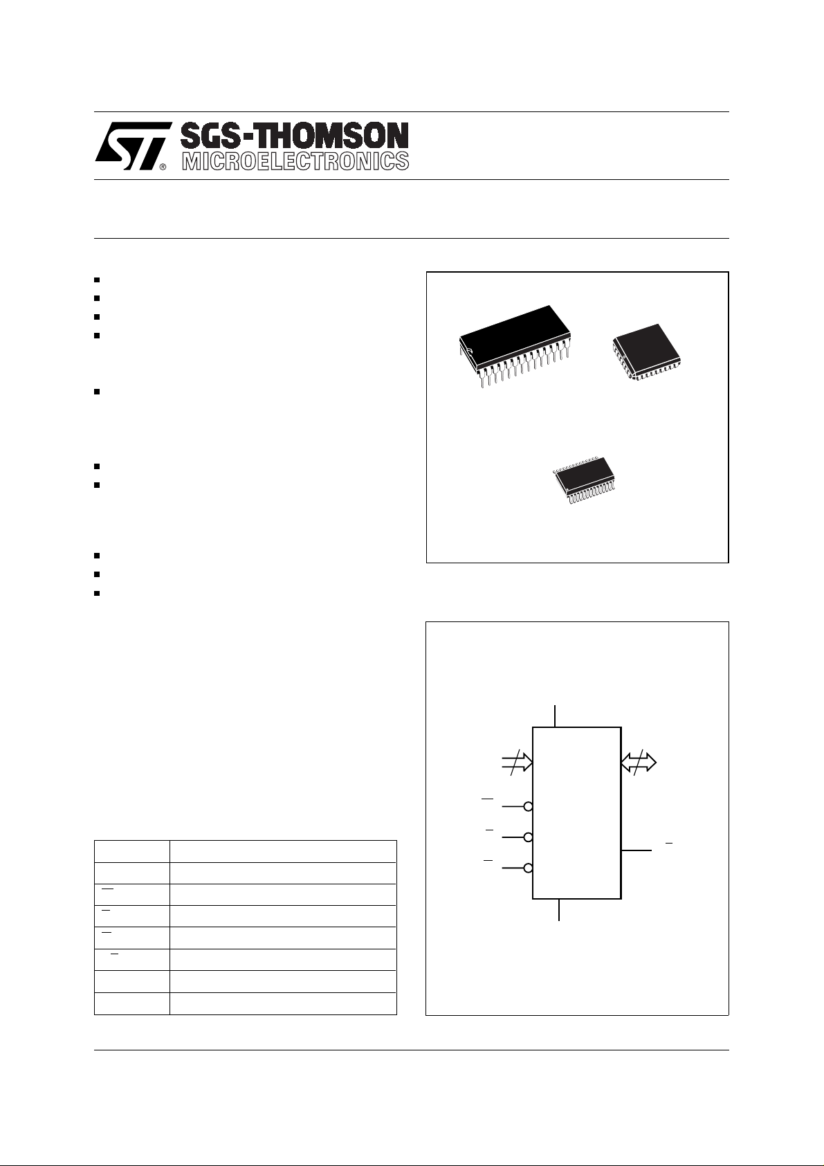
16K (2K x 8) PARALLEL EEPROM
NOT FOR NEW DESIGN
28
1
PDIP28 (P) PLCC32 (K)
28
1
SO28 (MS)
300 mils
Figure 1. Logic Diag ra m
DESCRIP T ION
The M28C17 is a 2K x 8 low power Parallel
EEPROM fabricated with SGS-THOMSON proprietary single polysilicon CMOS technology. The
V
CC
device offers fast access time with low power dissipation and requires a 5V power supply.
The M28C17 offers the same features than the
M28C16, in addition to the Ready/Busy pin.
11
A0-A10
8
DQ0-DQ7
The circuit has been designed to offer a flexible
microcontroller interface featuring both hardware
W
T able 1. Signal Names
A0 - A10 Address Input
DQ0 - DQ7 Data Input / Output
W Write Enable
E Chip Enable
G Output Enable
B Ready / Busy
R
V
CC
V
SS
November 1997 1/17
This is information on a product still in production but not recommended for new design.
Supply Voltage
Ground
E
G
M28C17
V
SS
RB
AI01487
Page 2
M28C17
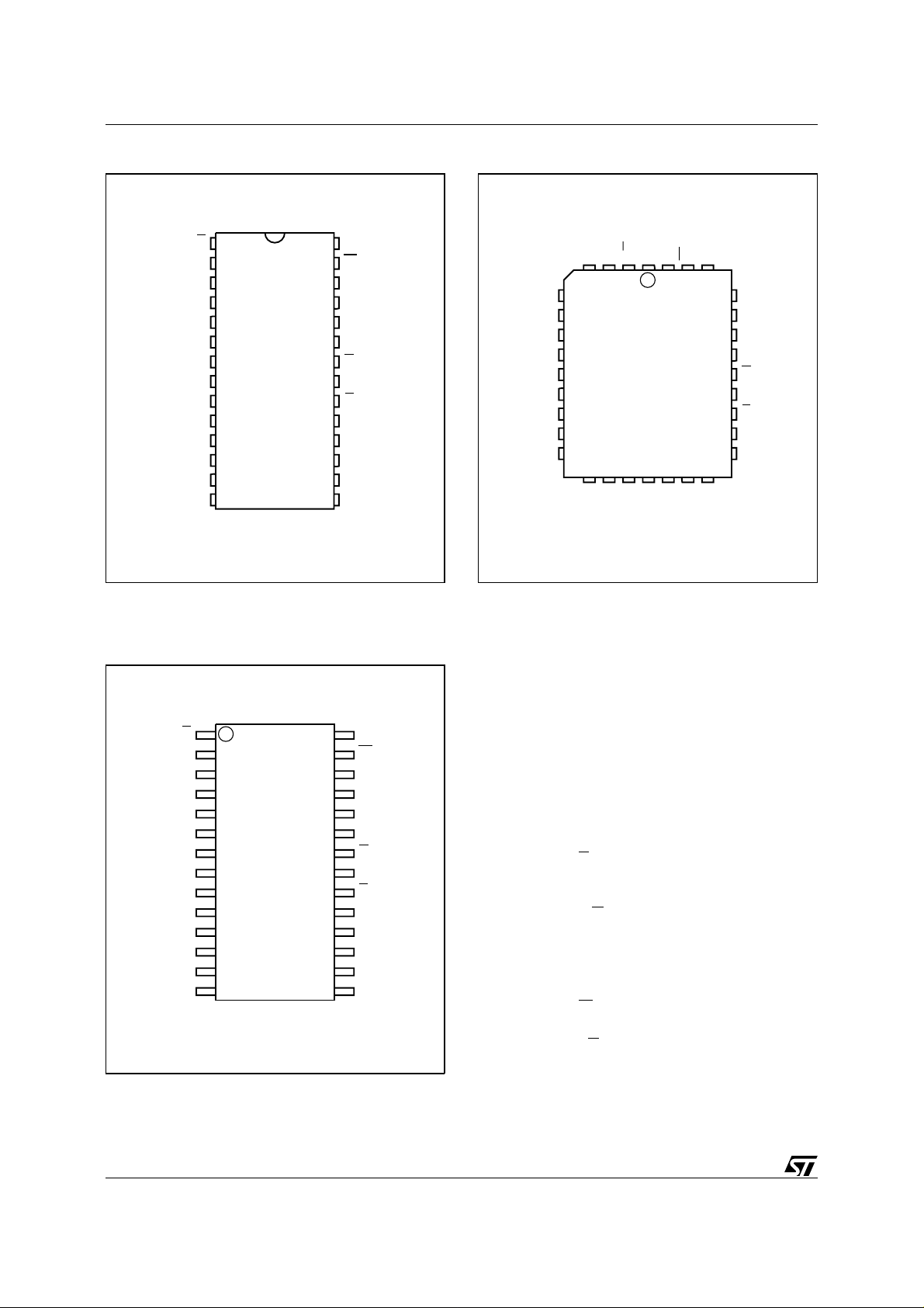
Figure 2A. DIP Pin Connectio ns
RB V
1
NC
2
3
A7
4
A6
5
A5
6
A4
7
A3
A2
A1
A0
DQ0
DQ2
SS
Warning: NC = Not Connected.
8
9
10
11
12
13
14
M28C17
28
27
26
25
24
23
22
21
20
19
18
17
16
15
AI01506B
CC
W
NC
A8
A9
NC
G
A10
E
DQ7
DQ6
DQ5DQ1
DQ4
DQ3V
Figure 2B. LCC Pin Connections
CC
NC
DU
32
W
V
A8
A9
NC
NC
G
25
A10
E
DQ7
DQ6
DQ4
DQ5
AI01508C
RB
A7
NC
A6
A5
A4
A3
A2
9
A1
A0
NC
DQ0
DQ1
Warning: NC = Not Connected, DU = Don’t Use.
1
M28C17
17
SS
V
DQ2DUDQ3
Figure 2C. SO Pin Connecti ons
A7
A6
A5
A4
A3
A2
A1
A0
1
2
3
4
5
6
7
8
9
10
11
12
13
14
M28C17
RB
NC
DQ0
DQ1
DQ2
V
SS
Warning: NC = Not Connected.
28
27
26
25
24
23 NC
22
21
20
19
18
17
16
15
AI01507B
V
CC
W
NC
A8
A9
G
A10
E
DQ7
DQ6
DQ5
DQ4
DQ3
DESCRIPTION (cont’d)
and software handshaking with Ready/Busy, Data
Polling and Toggle Bit. The M28C17 supports 64
byte page write operation. A Sof tware Data Prot ection (SDP) is also possible using the standard
JEDEC algorithm .
PIN DESCRIPTION
Addresses (A0-A10). The address inputs select
an 8-bit memory location during a read or write
operation.
Chip Enable (
E). The chip enable input must be
low to enable all read/write operations. Wh en Chip
Enable is high, power consumption is reduced.
Output Enable (
G). The Output Enable input con-
trols the data output buffers and is used to initiate
read operations.
Data In/ Out (DQ0 - DQ7). Data is writ ten to or read
from the M28C17 through the I/O pins.
Write E nable (
W). The Write En able input cont rols
the writing of data to the M28C17.
Ready/Busy (R
B). Ready/Busy is an open drain
output that can be used to detect the end of the
internal write cycle.
2/17
Page 3
M28C17
T ab le 2. Absolut e Maximu m Ra t ings
Symbol Parameter Value Unit
T
T
STG
V
CC
V
IO
V
V
ESD
Note: 1. Except for the rating "Operating T emperature Range", stresses above those listed in the Table "Absolute Maximum Ratings" may
2. 100pF through 1500Ω; MIL-STD-883C, 3015.7
T ab le 3. Operating Modes
Standby 1 X X Hi-Z
Output Disable X 1 X Hi-Z
Write Disable X X 1 Hi-Z
Ambient Operating Temperature – 40 to 125 °C
A
Storage Temperature Range – 65 to 150 °C
Supply Voltage – 0.3 to 6.5 V
Input/Output Voltage – 0.3 to VCC +0.6 V
Input Voltage – 0.3 to 6.5 V
I
Electrostatic Discharge Voltage (Human Body model)
cause permanent damage to the device. These are stress ratings only and operation of the device at these or any other conditions
above those indicated in the Operating sections of this specif icat ion is not implied. Expos ure to Absolut e Maximum Rating
conditions for extended periods may affect device reliability. Refer also to the SGS-THOMSON SURE Program and other
relevant quality documents.
(1)
Mode E G W DQ0 - DQ7
(1)
(2)
4000 V
Read 0 0 1 Data Out
Write 0 1 0 Data In
Chip Erase 0 V 0 Hi-Z
Note: 1. 0 = VIL; 1 = VIH; X = VIL or V
OPERATION
In order to prevent data corruption and inadv ertent
write operations an internal V
Write operation if V
is below VWI (see Table 7).
CC
Access to the mem ory in write mode is allowed after
a power-up as specified in Table 7.
Read
The M28C17 is acces sed like a stat ic RAM. W hen
E and G are low with W high, the data addressed
is presented on the I/O pins. The I/O pins are high
impedance when either
Write
Write operations are initiated when both
are low and
G is high.The M28C17 supports both
E and W controlled write cycles. The Address is
latched by the falling edge of
occurs last and the Data on the rising edge of
W which ever occurs first. Once initiated the write
V = 12 ± 5%.
IH;
comparator inhibits
CC
G or E is high.
E or W which ever
W and E
E or
Page Write
Page write allows up to 64 bytes to be consecutively latched into the memory prior to initiating a
programming cycle. All bytes must be located in a
single page address, that is A6-A10 must be the
same for all byt es. The page wr ite c an be initiat e d
during any byte write operation.
Following the first byte write instruction the host
may send another address and data with a minimum data transfer rate of 1/t
If a transition of
E or W is not detected within t
(see Figure 13).
WHWH
the internal programming cycle will start.
Chip Erase
The contents of the entire memory m ay be eras ed
to FFh by use of the Chip Erase command by
setting Chip Enable (
G) to VCC + 7.0V . The chip is cleared when a 10ms
(
E) Low and Output Enable
low pulse is applied to the Write Enable pin.
operation is internally timed until completion.
WHWH
,
3/17
Page 4
M28C17
Figure 3. Block Diagram
RB E G W
A6-A10
(Page Address)
A0-A5
VPP GEN RESET
ADDRESS
LATCH
ADDRESS
LATCH
Y DECODE
X DECODE
CONTROL LOGIC
64K ARRAY
SENSE AND DATA LATCH
I/O BUFFERS
DQ0-DQ7
PAGE LOAD
TIMER STATUS
TOGGLE BIT
DATA POLLING
AI01488
Microco ntroller Control Interface
The M28C17 provides two write operation status
bits and one status pin that can be used to minimize
the system write cyc le. These signals are available
on the I/O port bits DQ7 or DQ6 of the memory
during programming cycle on ly, or as the R
B signal
on a separate pin.
Figure 4. Status Bit Assignmen t
DQ7 DQ6 DQ5 DQ4 DQ3 DQ2 DQ1 DQ0
DP TB PLTS Hi-Z Hi-Z Hi-Z Hi-Z Hi-Z
DP = Data Polling
TB = Toggle Bit
PLTS = Page Load Timer Status
Data Polling bit (DQ7). During the internal write
cycle, any attempt to read the last byte written will
produce on DQ7 the complementary value of the
previously latched bit. Once the write cycle is fin-
4/17
ished the true logic value appears on DQ7 in the
read cycle.
T oggle bit ( DQ6). The M28C17 offers another way
for determining when the internal write cycle is
completed. During the internal Erase/Write cycle,
DQ6 will toggle from "0" to "1" and "1" to "0" (the
first read value is "0") on subsequent attempts to
read the memory. When the internal cycle is completed the toggling will stop and the device will be
accessible for a new Read or Write operation.
Page Load Timer Status bit (DQ5). In the Page
Write mode data may be latched by
E or W. Up to
64 bytes may be input. The Data output (DQ5)
indicates the status of the internal Page Load
Timer. DQ5 may be read by asserting Output Enable Low (t
). DQ5 Low indicates the timer is
PLTS
running, High indicates time-out after which the
write cycle will start and no new data may be input.
Ready/Busy pin. The R
B pin provides a signal at
its open drain output which is low during the
erase/write cycle, but which is released at the
completion of the programming cycle.
Page 5
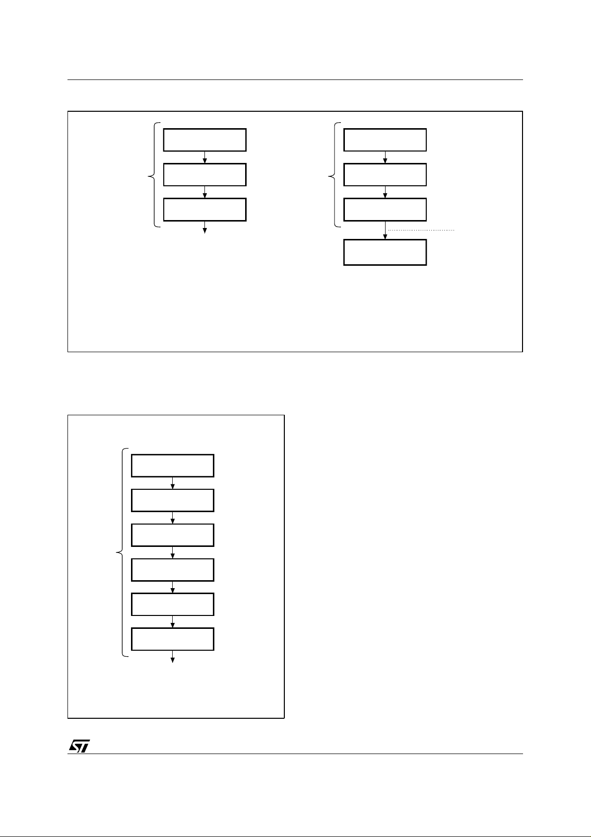
Figure 5. Software Data Protectio n Enabl e Algor ithm an d Memo ry Wr ite
M28C17
WRITE AAh in
Address 555h
Page
Write
Instruction
(Note 1)
Note: 1. MSB Address bits (A6 to A10) differ during these specific Page Write operations.
WRITE 55h in
Address 2AAh
WRITE A0h in
Address 555h
SDP is set
SDP ENABLE ALGORITHM
Figure 6. Software Data Protectio n Disabl e
Algo rith m
Page
Write
Instruction
(Note 1)
Software Data Protection
The M28C17 offers a software controlled write
protection facility that allows the user to inhibit all
write modes to the device including the Chip Erase
instruction. This can be useful in protecting the
memory from inadvertent write cycles that may
WRITE AAh in
Address 555h
occur due to uncontrolled bus conditions.
The M28C17 is shipped as standard in the "unpro-
tected" state meaning that the memory contents
WRITE 55h in
Address 2AAh
can be changed as required by the user. After the
Software Data Protection enable algorithm is issued, the device enters the "Protect Mode" of
operation where no further write commands have
any effect on the memory contents. The device
remains in this mode until a valid Software Data
Protection (SDP) disable sequence is received
whereby the device reverts to its "unprotected"
state. The Software Data Protection is fully non-
Page
Write
Instruction
WRITE 80h in
Address 555h
WRITE AAh in
Address 555h
volatile and is not changed by power on/off se-
WRITE 55h in
Address 2AAh
quences.
To enable the Software Data Protection (S DP) the
device requires the user to write (with a Page Write)
WRITE 20h in
Address 555h
three specific data bytes to three specific memory
locations as per Figure 5. Similarly to disable the
Software Data Protection the user has to write
Unprotected State
AI01510
specific data bytes into six different locations as per
Figure 6 (with a Page Write). This complex series
ensures that the user will never enable or disable
the Software Data Protection acc identally.
WRITE AAh in
Address 555h
WRITE 55h in
Address 2AAh
WRITE A0h in
Address 555h
WRITE
is enabled
Write Page
(1 up to 64 bytes)
WRITE IN MEMORY
WHEN SDP IS SET
AI01509B
5/17
Page 6
M28C17
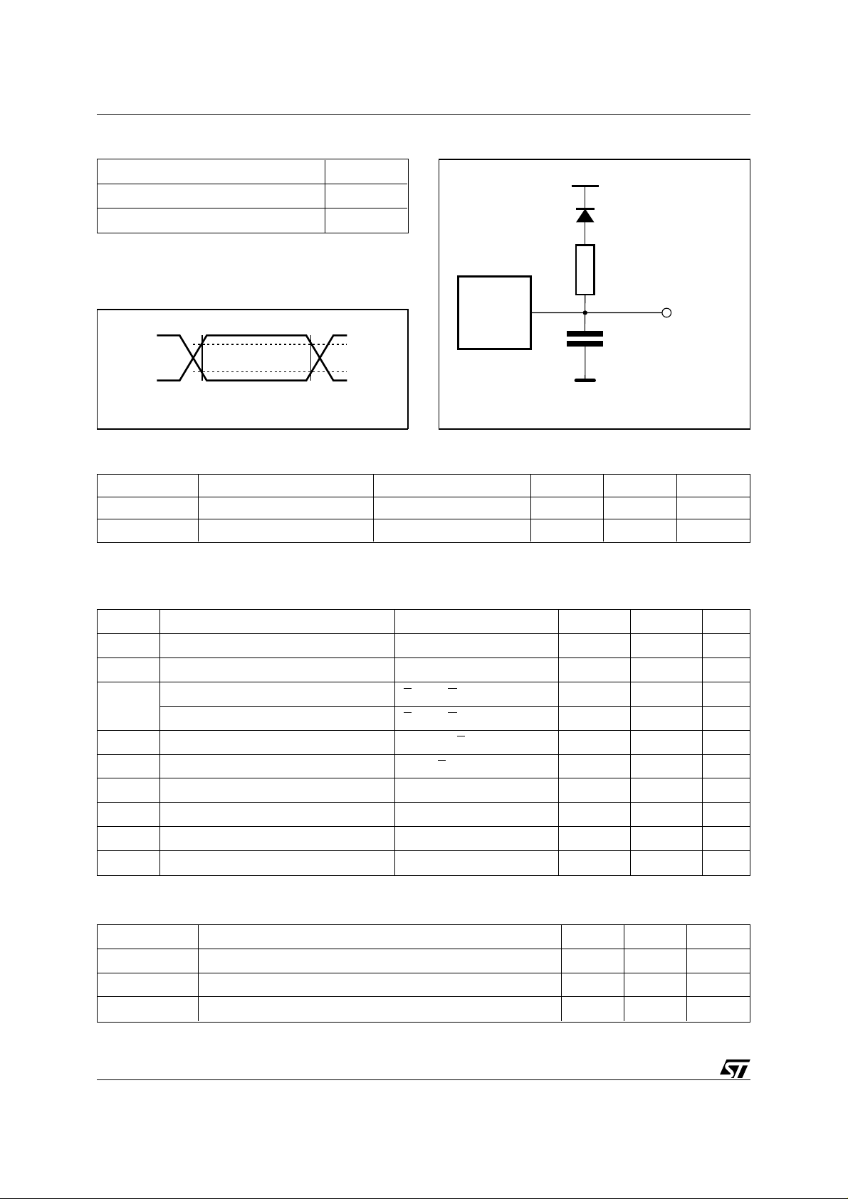
T ab le 4. AC Measurement Con ditions
Input Rise and Fall Times ≤ 20ns
Figure 8. AC Testing Equival ent Load Circu it
1.3V
Input Pulse Voltages 0.4V to 2.4V
Input and Output Timing Ref. Voltages 0.8V to 2.0V
Note that Output Hi-Z is defined as the point where data is no
longer driven.
Figure 7. AC T esti ng Inpu t Outp ut W avefo r ms
2.4V
0.4V
T ab le 5. Capacitance
(1)
(TA = 25 °C, f = 1 MHz )
2.0V
0.8V
AI00826
DEVICE
UNDER
TEST
CL includes JIG capacitance
1N914
3.3kΩ
CL = 30pF
Symbol Parameter Test Condition Min Max Unit
C
IN
C
OUT
Note: 1. Sampled only, not 100% test ed.
Input Capacitance VIN = 0V 6 pF
Output Capacitance V
= 0V 12 pF
OUT
OUT
AI01129
T ab le 6. Read Mode DC Characteristics
= 0 to 70°C or –40 to 85°C; VCC = 4.5V to 5.5V)
(T
A
Symbol Parameter Test Condition Min Max Unit
I
I
I
CC
I
CC1
I
CC2
V
V
V
V
Note: 1. All I/O’s open circuit.
T a b le 7. Power Up Timi n g
Note: 1. Sampled only, not 100% test ed.
Input Leakage Current 0V ≤ VIN ≤ VCC 10 µA
LI
Output Leakage Current 0V ≤ VIN ≤ VCC 10 µA
LO
Supply Current (TTL inputs) E = VIL, G = VIL , f = 5 MHz 30 mA
(1)
Supply Current (CMOS inputs)
(1)
Supply Current (Standby) TTL E = V
(1)
Supply Current (Standby) CMOS E > VCC –0.3V 100 µA
Input Low Voltage – 0.3 0.8 V
IL
Input High Voltage 2 VCC +0.5 V
IH
Output Low Voltage IOL = 2.1 mA 0.4 V
OL
Output High Voltage IOH = –400 µA 2.4 V
OH
(1)
(TA = 0 to 70°C or –40 to 85°C)
E = VIL, G = VIL , f = 5 MHz 25 mA
IH
1mA
Symbol Parameter Min Max Unit
t
PUR
t
PUW
V
WI
Time Delay to Read Operation 1 µs
Time Delay to Write Operation (once VCC ≥ 4.5V) 10 ms
Write Inhibit Threshold 3.0 4.2 V
6/17
Page 7

T ab le 8. Read Mode AC Charact eristics
= 0 to 70°C or –40 to 85°C; VCC = 4.5V to 5.5V)
(T
A
M28C17
Symbol Alt Parameter
Test
Condition
min max min max min max
t
AVQV
t
ELQV
t
GLQV
(1)
t
EHQZ
(1)
t
GHQZ
t
AXQX
Note: 1. Output Hi-Z is defined as the point at which data is no longer driven.
Address Valid to
t
ACC
Output Valid
Chip Enable Low to
t
CE
Output Valid
Output Enable Low
t
OE
to Output Valid
Chip Enable High
t
DF
to Output Hi-Z
Output Enable High
t
DF
to Output Hi-Z
Address Transition
t
OH
to Output Transition
E = VIL,
G = VIL
G = VIL 90 120 150 ns
E = VIL 40 45 50 ns
G = VIL 040045050ns
E = V
E = VIL,
G = V
IL
IL
040045050ns
000ns
Figure 9. Read Mode AC Wavefo r ms
M28C17
-90 -120 -150
90 120 150 ns
Unit
A0-A10
E
G
DQ0-DQ7
Note: Write Enable (W) = High
VALID
tAVQV tAXQX
tGLQV tEHQZ
tELQV
DATA OUT
tGHQZ
Hi-Z
AI01511B
7/17
Page 8

M28C17
T ab le 9. Writ e Mode AC Characteri stics
= 0 to 70°C or –40 to 85°C; VCC = 4.5V to 5.5V)
(T
A
Symbol Alt Parameter Test Condition Min Max Unit
t
AVWL
t
AVEL
t
ELWL
t
GHWL
t
GHEL
t
WLEL
t
WLAX
t
ELAX
t
WLDV
t
ELDV
t
ELEH
t
WHEH
t
WHGL
t
EHGL
t
EHWH
t
t
t
t
t
t
t
t
t
AS
t
AS
CES
OES
OES
WES
t
AH
t
AH
t
DV
t
DV
t
WP
CEH
OEH
OEH
WEH
Address Valid to Write Enable Low E = VIL, G = V
Address Valid to Chip Enable Low G = VIH, W = V
Chip Enable Low to Write Enable Low G = V
Output Enable High to Write Enable
Low
Output Enable High to Chip Enable Low W = V
Write Enable Low to Chip Enable Low G = V
E = V
IH
IL
IL
IH
IH
IL
0ns
0ns
0ns
0ns
0ns
0ns
Write Enable Low to Address Transition 50 ns
Chip Enable Low to Address Transition 50 ns
Write Enable Low to Input Valid E = VIL, G = V
Chip Enable Low to Input Valid G = VIH, W = V
IH
IL
1 µs
1 µs
Chip Enable Low to Chip Enable High 50 ns
Write Enable High to Chip Enable High 0 ns
Write Enable High to Output Enable
Low
0ns
Chip Enable High to Output Enable Low 0 ns
Chip Enable High to Write Enable High 0 ns
t
WHDX
t
EHDX
t
WHWL
t
WLWH1
t
WHWH
t
WHRH
t
WHRL
t
EHRL
t
DVWH
t
DVEH
Note: 1. With a 3.3 kΩ external pull-up resistor.
t
t
t
WPH
t
t
BLC
t
WC
t
t
t
t
DH
DH
WP
DB
DB
DS
DS
Write Enable High to Input Transition 0 ns
Chip Enable High to Input Transition 0 ns
Write Enable High to Write Enable Low 50 ns
Write Enable Low to Write Enable High 50 ns
Byte Load Repeat Cycle Time 0.15 100 µs
Write Cycle Time 3 ms
Write Enable High to Ready/Busy Low Note 1 150 ns
Chip Enable High to Ready/Busy Low Note 1 150 ns
Data Valid before Write Enable High 50 ns
Data Valid before Chip Enable High 50 ns
8/17
Page 9

Figure 10. Wr ite Mo de AC W avefo rms - Wri te En ab le Con tro lled
M28C17
tAVWL
tELWL
VALID
tWLAX
tWLDV
DATA IN
A0-A10
E
G
tGHWL
W
DQ0-DQ7
RB
Figure 1 1. W rite Mod e AC Wavef orm s - Chip En able Co ntro lled
tWHEH
tWHGLtWLWH1
tWHWL
tWHDXtDVWH
tWHRL
AI01128
A0-A10
E
G
W
DQ0-DQ7
RB
tAVEL
tGHEL
tWLEL
VALID
tELAX
tELDV
tELEH
tEHGL
tEHWH
DATA IN
tEHDXtDVEH
tEHRL
AI01513
9/17
Page 10

M28C17
Figure 12. Page W rite Mod e AC Wavefo r m s - Wri te En ab le Con tro lled
A0-A10
E
G
W
DQ0-DQ7
DQ5
RB
tWLWH
Addr 0
tWHWL
Byte 0 Byte 1 Byte 2 Byte n
Addr 1 Addr 2 Addr n
tWHWH
tWHRL
tPLTS
tWHRH
tWHWH
Byte n
AI01514
Figure 13. Sof tware Protected Write Cycle Waveforms
G
E
tWLWH
W
tAVEL
A0-A5
A6-A10
DQ0-DQ7
Note: A6 through A10 must specify the same page address during each high to low transition of W (or E) after the software code has been
G must be high only when W and E are both low.
entered.
555h 2AAh 555h
tWLAX
tWHDX
tDVWH
tWHWL
Byte Address
Page Address
Byte 0
tWHWH
Byte 62 Byte 63AAh 55h A0h
AI01515
10/17
Page 11

Figure 14. Data Polling W avefo rm Seq u ence
M28C17
A0-A10
E
G
W
DQ7
LAST WRITE INTERNAL WRITE SEQUENCE
Address of the last byte of the Page Write instruction
DQ7 DQ7DQ7 DQ7DQ7
Figure 15. Toggle Bit Wavefor m Sequ en ce
READY
AI01516
A0-A10
E
G
W
DQ6
Note: 1. First T oggle bit is forced to ’0’.
(1)
TOGGLE
INTERNAL WRITE SEQUENCE
READYLAST WRITE
AI01517
11/17
Page 12

M28C17
Figure 16. Chip Erase Wavforms
E
G
W
tWHEH
tGLWH
tWLWH2tELWL
tWHRH
AI01484B
T ab le 10. Chip Er ase AC Characteri sti cs
= 0 to 70°C or –40 to 85°C; VCC = 4.5V to 5.5V)
(T
A
Symbol Parameter Test Condition Min Max Unit
t
ELWL
t
WHEH
t
WLWH2
t
GLWH
t
WHRH
Chip Enable Low to Write Enable Low G = VCC + 7V 1 µs
Write Enable High to Chip Enable High G = VCC + 7V 0 ns
Write Enable Low to Write Enable High G = VCC + 7V 10 ms
Output Enable Low to Write Enable High G = VCC + 7V 1 µs
Write Enable High to Write Enable Low G = VCC + 7V 3 ms
12/17
Page 13

ORDERING INFORMATION SCHEME
Example: M28C17 -90 K 1 T
M28C17
Speed
-90 90ns
-120 120ns
-150 150ns
Package
P PDIP28
K PLCC32
MS SO28 300mils
Temperature Range
1 0 to 70 °C
6 –40 to 85 °C
Option
T Tape & Reel
Packing
Devices are shipped from the factory with the memory content set at all "1’s" (FFh).
For a list of available options (Package, etc...) or for further informat ion on any aspect of this device, please
contact the SGS-THO MS O N Sales Offic e nearest to you.
13/17
Page 14

M28C17
PDIP28 - 28 pin Plastic DIP, 600 mils width
Symb
Typ Min Max Typ Min Max
A 3.94 5.08 0.155 0.200
A1 0.38 1.78 0.015 0.070
A2 3.56 4.06 0.140 0.160
B 0.38 0.56 0.015 0.021
B1 1.14 1.78 0.045 0.070
C 0.20 0.30 0.008 0.012
D 34.70 37.34 1.366 1.470
E 14.80 16.26 0.583 0.640
E1 12.50 13.97 0.492 0.550
e1 2.54 – – 0.100 – –
eA 15.20 17.78 0.598 0.700
L 3.05 3.82 0.120 0.150
S 1.02 2.29 0.040 0.090
α 0° 15° 0° 15°
N28 28
PDIP28
mm inches
Drawing is not to scale.
14/17
B1 B e1
D
S
N
1
A2
A1AL
Cα
eA
E1 E
PDIP
Page 15

PLCC32 - 32 lead Plastic Leaded Chip Carrier, rectangular
M28C17
Symb
Typ Min Max Typ Min Max
A 2.54 3.56 0.100 0.140
A1 1.52 2.41 0.060 0.095
B 0.33 0.53 0.013 0.021
B1 0.66 0.81 0.026 0.032
D 12.32 12.57 0.485 0.495
D1 11.35 11.56 0.447 0.455
D2 9.91 10.92 0.390 0.430
E 14.86 15.11 0.585 0.595
E1 13.89 14.10 0.547 0.555
E2 12.45 13.46 0.490 0.530
e 1.27 – – 0.050 – –
j 0.89 – – 0.035 – –
N32 32
Nd 7 7
Ne 9 9
CP 0.10 0.004
PLCC32
mm inches
Ne
Drawing is not to scale.
PLCC
D
D1
1 N
Nd
E1 E
D2/E2
A1
j
B1
e
B
A
CP
15/17
Page 16

M28C17
SO28 - 28 lead Plastic Small Outline, 300 mils body width
Symb
Typ Min Max Typ Min Max
A 2.46 2.64 0.097 0.104
A1 0.13 0.29 0.005 0.011
A2 2.29 2.39 0.090 0.094
B 0.35 0.48 0.014 0.019
C 0.23 0.32 0.009 0.013
D 17.81 18.06 0.701 0.711
E 7.42 7.59 0.292 0.299
e 1.27 – – 0.050 – –
H 10.16 10.41 0.400 0.410
L 0.61 1.02 0.024 0.040
α 0° 8° 0° 8°
N28 28
CP 0.10 0.004
SO28
mm inches
Drawing is not to scale.
16/17
A2
A
C
B
e
CP
D
N
E
H
1
LA1 α
SO-b
Page 17

M28C17
Information furnished is believed to be accurate and reliable. However, SGS-THOMSON Microelectronics assumes no responsibility for the
consequences of use of such information nor for any infringement of patents or other rights of third parties which may result from its use. No
license is granted by implication or otherwise under any patent or patent rights of SGS-THOMSON Microelectronics. Specifications mentioned
in this publication are subject to change without notice. This publication supersedes and replaces all information previously supplied.
SGS-THOMSON Microelectronics products are not authorized for use as critical components in life support devices or systems with out express
written approval of SGS-THOMSON Microelectronics.
© 1997 SGS-THOMSON Microelectronics - All Rights Reserved
Australia - Brazil - Canada - China - France - Germany - Italy - Japan - Korea - Malaysia - Malta - Morocco - The Netherlands -
Singapore - Spain - Sweden - Switzerland - Taiwan - Thailand - United Kingdom - U.S.A.
SGS-THOMSON Microelectronics GROUP OF COMPANIES
17/17
 Loading...