

Page 1
Low Voltage UV EPROM and OTP EPROM
■ 2.7V to 3.6V LOW VOLTAGE in READ
OPERATION
■ ACCESS TIME:
–90ns at V
– 100ns at V
■ BYTE-WIDE or WORD-WIDE
CONFIGURABLE
■ 8 Mbit MASK ROM REPLACEMENT
■ LOW POWER CONSUMPTION
– Active Current 30mA at 8MHz
– Standby Current 15µA
■ PROGRAMMI N G VOLT AG E: 1 2.5V ± 0.25V
■ PROGRAMMING TIME: 50µs/word
■ ELECTRONIC SIGNATURE
– Manufacturer Code: 20h
– Device Code: B2h
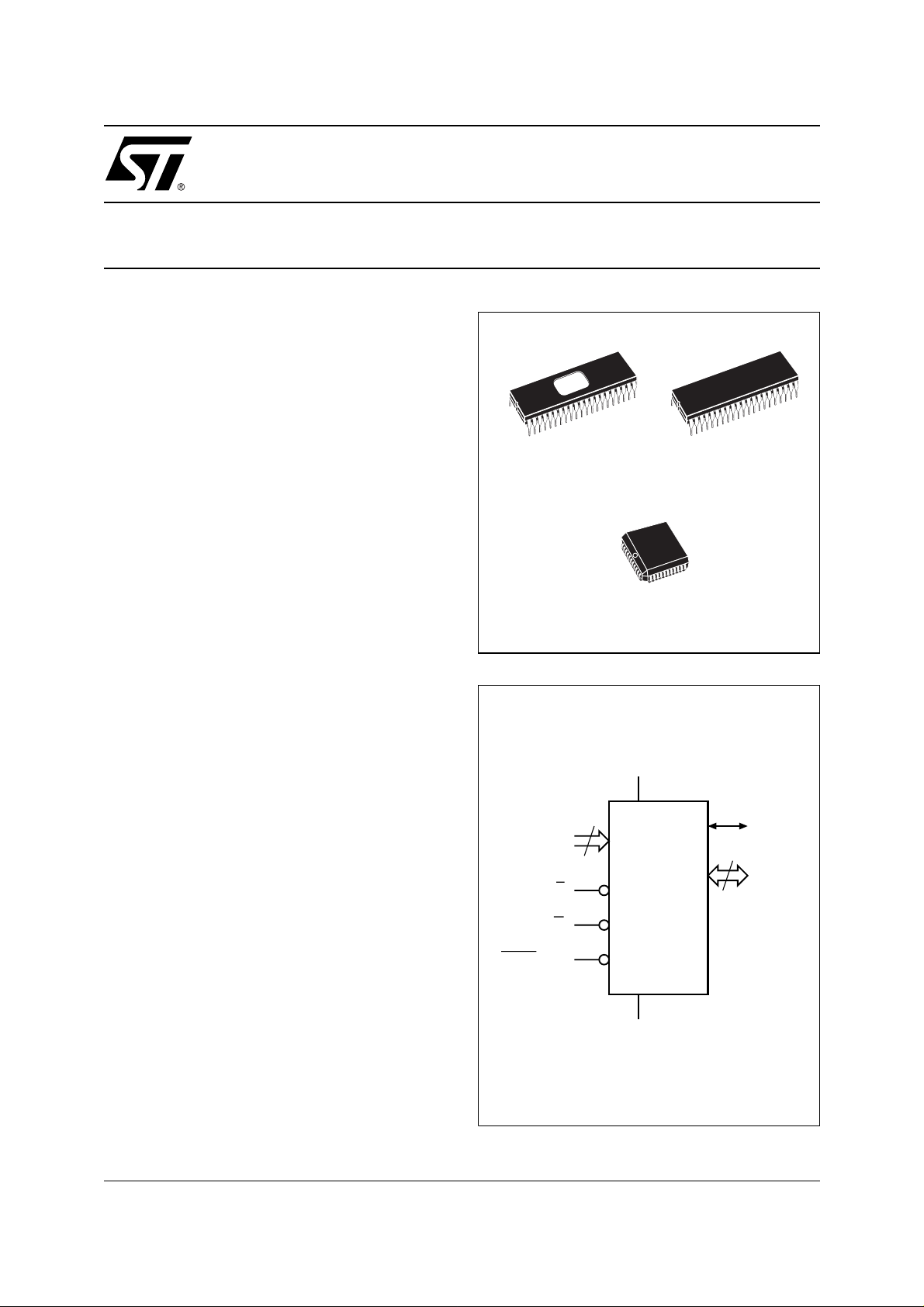
DESCRIPTION
The M27W800 is a low voltage 8 Mbit EPROM offered in the two ranges UV (ultra violet erase) and
OTP (one time programmab le). It is ideally suited
for microprocessor systems requiring large data or
program storage. It is orga nised as either 1 M bit
words of 8 bit or 512 Kbit words of 16 bit. The pinout is compatible with a 8 Mbit Mask ROM.
The M27W800 operates in the read mode with a
supply voltage as low as 2.7V. The decrease in
operating power allows either a red uction of the
size of the battery or an increase i n the time between battery recharges.
The FDIP42W (window ceramic frit-seal package)
has a transparent lid which all ows the user to expose the chip to ultraviolet light to erase the bit pattern. A new pattern can then be written rapidly to
the device by following the programming procedure.
For applications where the content is programmed
only one time and erasure is not required, the
M27W800 is offered in PDIP42 and PLCC44 package.
= 3.0V to 3.6V
CC
= 2.7V to 3.6V
CC
M27W800
8 Mbit (1Mb x 8 or 512Kb x 16)
42
1
FDIP42W (F) PDIP42 (B)
Figure 1. Logic Diagram
19
A0-A18
E
G
BYTEV
PP
42
PLCC44 (K)
V
CC
M27W800
V
SS
1
Q15A–1
15
Q0-Q14
AI03601
1/15March 2000
Page 2
M27W800
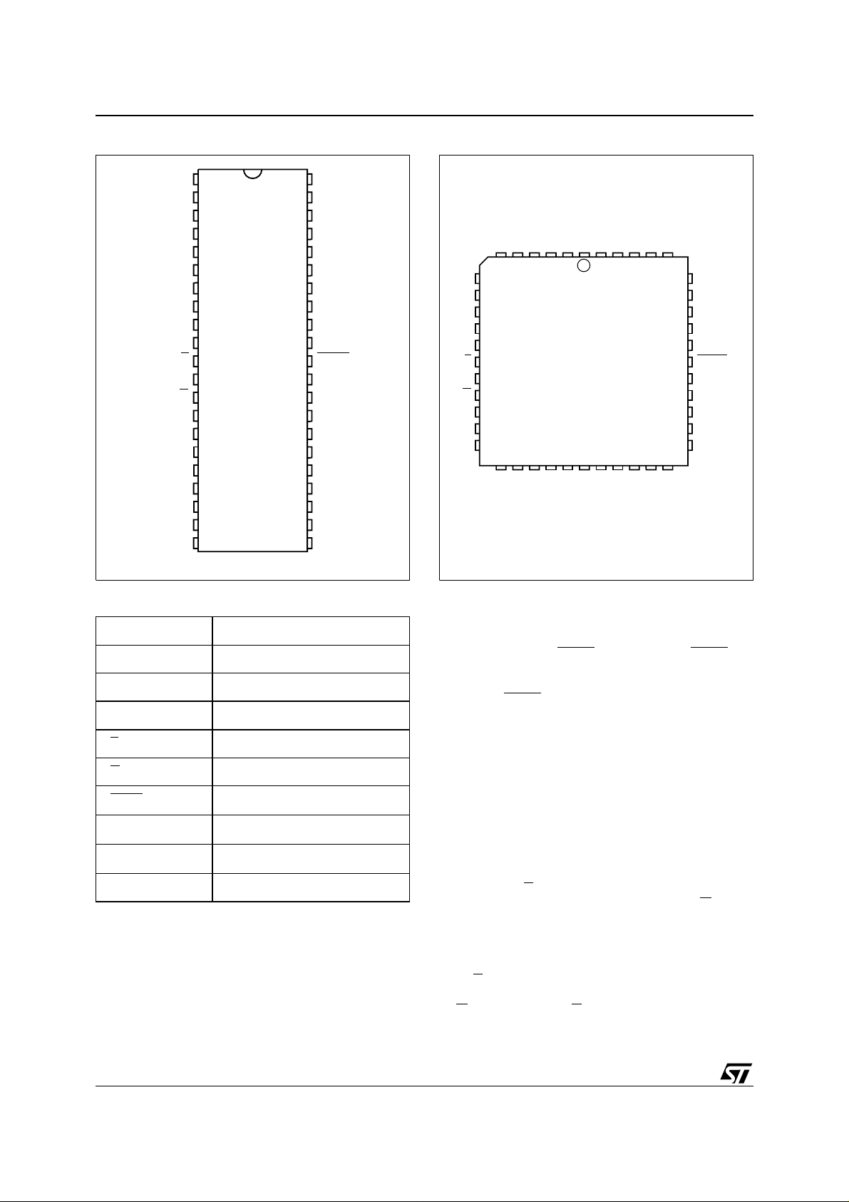
Figure 2A. DIP Connections
A18 NC
1
2
A7
3
4
A6
5
A5
A4
6
7
A3
A2
8
9
A1
10
A0
V
SS
Q0
Q8
Q1
Q9
Q10
Q3
Q11
E
G
M27W800
11
12
13
14
15
16
17
18
19
20
21
42
41
40
39
38
37
36
35
34
33
32
31
30
29
28
27
26
25
24
23
22
AI03602
A8A17
A9
A10
A11
A12
A13
A14
A15
A16
BYTEV
V
SS
Q15A-1
Q7
Q14
Q6
Q13
Q5Q2
Q12
Q4
V
CC
PP
Figure 2B. LCC Connections
A7
A5
A6
A4
A3
A2
A1 A15
A0
E
12
V
SS
Q0
Q8
Q1
Q9
Q2
Q10
SS
A18
A17
V
1
44
M27W800
23
Q3
NC
Q11
NC
CC
V
A8
Q4
A9
Q12
A10
Q5
A11
34
Q13
A12
A13
A14
A16
BYTEV
V
SS
Q15A–1G
Q7
Q14
Q6
AI03603
PP
Table 1. Signal Names
A0-A18 Address Inputs
Q0-Q7 Data Outputs
Q8-Q14 Data Outputs
Q15A–1 Data Output / Address Input
E
G
V
BYTE
PP
V
CC
V
SS
NC Not Connected Internally
Chip Enable
Output Enable
Byte Mode / Program Supply
Supply Voltage
Ground
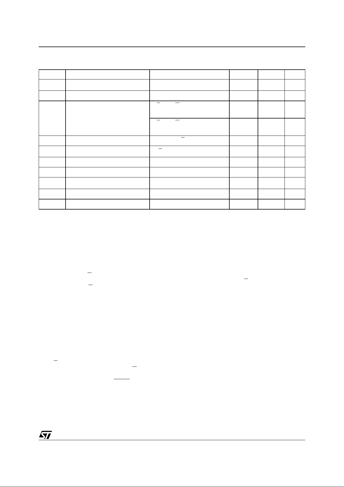
DEVICE OPERATION
The operating modes of the M27W800 are listed in
the Operating Modes Table. A single power supply
is required in the read mode. All inputs are TTL
compatib le exce pt for V
and 12V on A9 for the
PP
Electronic Signature.
Read Mode
The M27W800 has two organ isations, Word-w ide
and Byte-wide. The organisation is selected by the
signal level on the BYTE
VPP pin. When BYTEV
PP
is at VIH the Word-wide organisation is selected
and the Q15A–1 pin is used for Q15 Data Output.
When the BYTE
VPP pin is at VIL the Byte-wide organisation is selected and the Q15A–1 pin is used
for the Address Input A–1. When the memory is
logically regarded as 16 bit wid e, but read in the
Byte-wide organisation, then with A–1 at V
IL
the
lower 8 bits of the 16 bit data are selected and with
A–1 at V
the upper 8 bits of the 16 bit dat a are
IH
sele cte d.
The M27W800 has two cont rol functions, both of
which must be logically ac tive in order to obtain
data at the outputs. In addition the Word-wide or
Byte-wide organisation must be selected.
Chip Enable (E
used for device selection. Output Enable (G
) is the power control and should be
) is the
output control and should be used to gate data to
the output pins i ndependent of device selection.
Assuming that the addresses are s table, the address access time (t
from E
to output (t
ELQV
output after a delay of t
of G
, assuming that E has been low and the ad-
dresses have been stable for at least t
) is equal to the delay
AVQV
). Data is available at the
from the falling e dge
GLQV
AVQV-tGLQV
.
2/15
Page 3
M27W800
Table 2. Absolute Maximum Ratings
(1)
Symbol Parameter Value Unit
T
A
T
BIAS
T
STG
(2)
V
IO
V
CC
(2)
V
A9
V
PP
Note: 1. Except for the ratin g " Operati ng Temperat ure Range" , stresses above th ose liste d i n t he Table " A bsolute M aximum Ratings" may
cause permanent damage to the device. These are stress ratings only and operation of the device at these or any other conditions
above those indi cated in the Operating sections of this s pecification is not impli ed. Exposure to A bsolute M aximum Rating conditions for extended per iods may aff ect device reliabilit y. Refer also to the STMicroel ectronics SURE Program an d other relevan t qual ity docum en ts .
2. Min imum DC volta ge on In put or O utput is –0.5V with po ssible under shoot t o –2.0V f or a period less th an 20ns. Maximu m DC
voltage on Output is V
3. Depends on range.
Ambient Operating Temperature
Temperature Under Bias –50 to 125 °C
Storage Temperature –65 to 150 °C
Input or Output Voltage (except A9) –2 to 7 V
Supply Voltage –2 to 7 V
A9 Voltage –2 to 13.5 V
Program Supply Voltage –2 to 14 V
+0.5V with possible overshoot to VCC +2V for a period l ess than 20n s.
CC
(3)
–40 to 125 °C
Table 3. Operating Modes
Mode E
Read Word-wide
Read Byte-wide Upper
Read Byte-wide Lower
Output Disable
Program
V
IL
Verify
Program Inhibit
Standby
Electronic Signature
Note: X = VIH or VIL, VID = 12V ± 0.5V.
V
IL
V
IL
V
IL
V
IL
Pulse V
V
IH
V
IH
V
IH
V
IL
V
V
V
V
V
V
V
BYTEV
G
IL
IL
IL
IH
IH
IL
IH
V
IH
V
IL
V
IL
X X Hi-Z Hi-Z Hi-Z
V
PP
V
PP
V
PP
A9 Q15A–1 Q14-Q8 Q7-Q0
PP
X Data Out Data Out Data Out
X
X
V
IH
V
IL
Hi-Z Data Out
Hi-Z Data Out
X Data In Data In Data In
X Data Out Data Out Data Out
X Hi-Z Hi-Z Hi-Z
X X X Hi-Z Hi-Z Hi-Z
IL
V
IH
V
ID
Code Codes Codes
Table 4. Electronic Signature
Identifier A0
Manufacturer’s Code
Device Code
V
IL
V
IH
Q15
and
Q7
Q14
and
Q6
Q13
and
Q5
Q12
and
Q4
Q11
and
Q3
Q10
and
Q2
Q9
and
Q1
Q8
and Q0Hex Data
00100000 20h
10110010 B2h
3/15
Page 4
M27W800
Table 5. AC Measurement Conditions
High Speed Standard
Input Rise and Fall Times ≤ 10ns ≤ 20ns
Input Pulse Voltages 0 to 3V 0.4V to 2.4V
Input and Output Timing Ref. Voltages 1.5V 0.8V and 2V
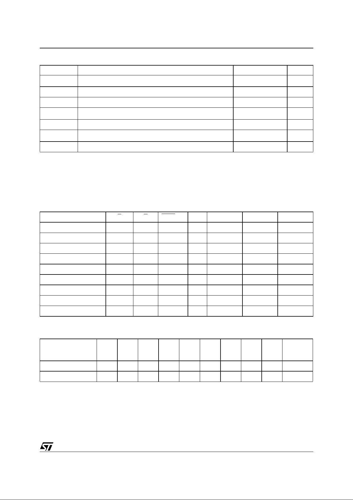
Figure 3. AC Testing Input Output Waveform
High Speed
3V
1.5V
0V
Standard
2.4V
0.4V
Table 6. Capacitance
(1)
(TA = 25 °C, f = 1 MHz)
2.0V
0.8V
AI01822
Figure 4. AC Testing Load Circuit
1.3V
1N914
3.3kΩ
DEVICE
UNDER
TEST
CL
CL = 30pF for High Speed
CL = 100pF for Standard
CL includes JIG capacitance
OUT
AI01823B
Symbol Parameter Test Condition Min Max Unit
C
Input Capacitance (except BYTEVPP)V
IN
C
OUT
Note: 1. Sampled only, not 100% tested.
Input Capacitance (BYTE
Output Capacitance
VPP)V
V
IN
IN
OUT
= 0V
= 0V
= 0V
10 pF
120 pF
12 pF
4/15
Page 5
M27W800
Table 7. Read Mode DC Characteristics
(1)
(TA = –40 to 85 °C; VCC = 2.7 to 3.6V; VPP = VCC)
Symbol Parameter Test Condition Min Max Unit
I
I
I
CC
I
CC1
I
CC2
I
V
V
IH
V
V
Note: 1. VCC must be ap pl i e d simultaneously wi th or before VPP and removed simultaneously or after VPP.
Input Leakage Current
LI
Output Leakage Curren t
LO
Supply Current
Supply Current (Standby) TTL
Supply Current (Standby) CMOS
Program Current
PP
Input Low Voltage –0.6
IL
(2)
Input High Voltage
Output Low Voltage
OL
Output High Voltage TTL
OH
2. Max imum DC volt age on Output i s V
CC
+0.5 V.
0V ≤ V
0V ≤ V
= VIL, G = VIL, I
E
f = 8MHz, V
E
= VIL, G = VIL, I
f = 5MHz, V
> VCC – 0.2V, VCC ≤ 3.6V
E
OUT
E
= V
V
PP
I
= 2.1mA
OL
I
= –400µA
OH
IN
= V
≤ V
≤ V
OUT
≤ 3.6V
CC
OUT
≤ 3.6V
CC
IH
CC
CC
CC
= 0mA,
= 0mA,
±1 µA
±10 µA
30 mA
20 mA
1mA
15 µA
10 µA
0.2V
CC
0.7V
2.4 V
CC
VCC + 0.5
0.4 V
V
V
Standby Mode
The M27W800 has a standby m ode which reduc-
es the supply current from 20mA to 20µA with low
voltage operation V
≤ 3.6V, see Read Mode DC
CC
Characteristics table for details.The M27W800 is
placed in the standby mode b y applying a CMOS
high signal to the E
input. When in the standby
mode, the outputs are in a h igh impedanc e state,
independent of the G
input.
Two Line Outp ut C ontrol
Because EPROMs are usually used in larger
memory arrays, this product features a 2 line control function which accommodates the use of multiple memory connection. The two line control
function allows:
a. the lowest possible memory power dissipation,
b. complete assurance tha t output bus contention
will not occur.
For the most efficient use of these two control
lines, E
ry device selecting function, while G
should be decoded and used as the prima-
should be
made a common connectio n to all devices in the
array and connected to the READ
line from the
system control bus. This ensures that all deselected memory devices are in their low power standby
mode and that the output pins are only active
when data is required from a particular memory
device.
System Considerations
The power switching characteristics of Advanced
CMOS EPROMs require careful decoupling of the
supplies to the devices. The supply current ICC
has three segments of importance to the system
designer: the standby current, the active current
and the transient peaks that are produced by the
falling and rising edges of E
. The magnitude of the
transient current peaks is dependent on the capacitive and inductive loadi ng of the device outputs. The associated transient voltage peaks can
be suppressed by complying with the two line output control and by properly selected decoupling
capacitors. It is recommended that a 0.1µF ceramic capacitor is used on every device between V
CC
and VSS. This should be a high frequency type of
low inherent inductance and should be placed as
close as possible to the device. In addition, a
4.7µF electrolytic capacitor should be used between V
and VSS for every eight devices. This
CC
capacitor should be mounted near the power supply connection point. The purpose of this capacitor
is to overcome the voltage d r op caus ed by the inductiv e effects of PCB traces.
5/15
Page 6

M27W800
Table 8. Read Mode AC Characteristics
(1)
(TA = –40 to 85 °C; VCC = 2.7 to 3.6V; VPP = VCC)
Symbol Alt Parameter Test Condition
t
AVQV
t
BHQV
t
ELQV
t
GLQV
t
BLQZ
t
EHQZ
t
GHQZ
(2)
(2)
(2)
Address Valid to
t
ACC
Output Valid
BYTE High to Output
t
ST
Valid
Chip Enable Low to
t
CE
Output Valid
Output Enable Low to
t
OE
Output Valid
BYTE Low to Output
t
STD
Hi-Z
Chip Enable High to
t
DF
Output Hi-Z
Output Enable High to
t
DF
Output Hi-Z
= VIL, G = V
E
= VIL, G = V
E
= V
G
= V
E
= VIL, G = V
E
= V
G
= V
E
M27W800
V
CC
-100
= 3.0 to
3.6V
(3)
VCC = 2.7 to
3.6V
-120
VCC = 2.7 to
3.6V
Unit
Min Max Min Max Min Max
IL
IL
IL
IL
IL
IL
IL
90 100 120 ns
90 100 120 ns
90 100 120 ns
45 50 60 ns
45 45 50 ns
045045050ns
045045050ns
Address Transition to
t
AXQX
t
BLQX
Note: 1. VCC must be ap pl i e d simultaneously wi th or before VPP and removed simultaneously or after V
2. Sampled only, not 100% tested.
3. Speed obtained with High Speed measu rement condi tions.
t
OH
Output Transition
BYTE Low to Output
t
OH
Transition
= VIL, G = V
E
= VIL, G = V
E
555ns
IL
555ns
IL
Figure 5. Word-Wide Read Mode AC Waveforms
A0-A18
E
G
Q0-Q15
tAVQV
tELQV
VALID
tAXQX
tGLQV
VALID
tEHQZ
tGHQZ
PP
Hi-Z
AI01596B
Note: BYTEVPP = VIH.
6/15
Page 7

Figure 6. Byte-Wide Read Mode AC Waveforms
M27W800
A–1,A0-A18
E
G
Q0-Q7
Note: BYTEVPP = V
IL.
VALID
tAVQV
tGLQV
tELQV
Figure 7. BYTE Transition AC Waveforms
A0-A18
VALID
tAXQX
tEHQZ
tGHQZ
Hi-Z
AI01597B
VALID
A–1
tAVQV
BYTEV
PP
Q0-Q7
tBLQX
Q8-Q15
tBLQZ
Note: Chip Ena bl e (E) and Output Enable (G ) = VIL.
VALID
tAXQX
tBHQV
DATA OUT
Hi-Z
DATA OUT
AI01598C
7/15
Page 8

M27W800
Table 9. Programming Mode DC Characteri stics
(1)
(TA = 25 °C; VCC = 6.25V ± 0.25V; VPP = 12.5V ± 0.25V)
Symbol Parameter Test Condition Min Max Unit
I
LI
I
CC
I
PP
V
V
V
OL
V
OH
V
Note: 1. VCC must be ap pl i e d simultaneously wi th or before VPP and removed simultaneously or after VPP.
Input Leakage Current
Supply Current 50 mA
Program Current
Input Low Voltage –0.3 0.8 V
IL
Input High Voltage 2.4
IH
Output Low Voltage
Output High Voltage TTL
A9 Voltage 11.5 12.5 V
ID
Table 10. Programming Mode AC Characteristics
0 ≤ V
E
= V
I
= 2.1mA
OL
I
= –2.5mA
OH
(1)
IN
≤ V
IL
CC
±1 µA
50 mA
V
+ 0.5
CC
0.4 V
3.5 V
TA = 25 °C; VCC = 6.25V ± 0.25V; VPP = 12.5V ± 0.25V)
Symbol Alt Parameter Test Condition Min Max Unit
t
AVEL
t
QVEL
t
VPHAV
t
VCHAV
t
ELEH
t
EHQX
t
QXGL
t
GLQV
(2)
t
GHQZ
t
GHAX
Note: 1. V
2. Sam pl ed only, not 100% tested .
t
Address Valid to Chip Enable Low 2 µs
AS
t
Input Valid to Chip Enable Low 2 µs
DS
t
t
t
t
t
must be ap pl i ed simultaneously wi th or before VPP and removed simultan eously or aft er VPP.
CC
VPP High to Address Valid
VPS
VCC High to Address Valid
VCS
Chip Enable Program Pulse Width 45 55 µs
PW
t
Chip Enable High to Input Transition 2 µs
DH
Input Transition to Output Enable Low 2 µs
OES
t
Output Enable Low to Output Valid 120 ns
OE
Output Enable High to Output Hi-Z 0 130 ns
DFP
Output Enable High to Address
t
AH
Transition
2µs
2µs
0ns
V
Programming
The M27W800 has been designed to be fully compatible with the M27C800 and has the same electronic signature. As a result the M27W800 can be
programmed as the M27C800 on the same programming equipments applying 12.75V on V
PP
and 6.25V on VCC by the use of t he same PRESTO III algorithm. When delivered (and after each
erasure for UV EPROM), all bits of the M27W800
are in the ’1’ state. Data is introduced by selective-
8/15
ly programming ’0’s into the desired bit locations.
Although only ’0’s will be programmed, both ’1’s
and ’0’s can be present in the data word. The only
way to change a ’0’ to a ’1’ i s by die exposure to ultraviolet light (UV EPROM). The M27W800 is in
the programming mode when V
12.5V, G
is at VIH and E is pulsed to VIL. The data
input is at
PP
to be programmed is applied to 16 bits in parallel
to the data output pins. The levels required for the
address and data inputs are TTL. V
is specified
CC
to be 6.25V ± 0.25V.
Page 9

Figure 8. Programming and Verify Mod es AC Wavefor ms
M27W800
A0-A18
Q0-Q15
BYTEV
PP
tVPHAV
V
CC
tVCHAV
E
G
Figure 9. Programming Flowchart
VCC = 6.25V, VPP = 12.5V
n = 0
E = 50µs Pulse
NO
NO
VERIFY
YES
NO
Last
Addr
YES
CHECK ALL WORDS
BYTEVPP =V
1st: VCC = 5V
2nd: VCC = 2.7V
IH
++ Addr
YES
++n
= 25
FAIL
VALID
tAVEL
DATA IN DATA OUT
tQVEL
tELEH
PROGRAM VERIFY
tEHQX
tQXGL
PRESTO III P rog ra m mi ng Algorithm
The PRESTO III Programming Algorithm allows
the whole array to be program ed with a guaranteed margin in a typical time of 26 secon ds. Programming with PRESTO I II con sists of a pplying a
sequence of 50µs program pulses to each word
until a correct verify occurs (see Figure 9). During
programing and verify operation a MARGIN
MODE circuit is automatically activated to guarantee that each cell is programed with e nough margin. No overprogram pulse is applied since the
verif y in MARG IN MO DE at V
3.6V provides the necessary margin to eac h programmed cell.
Program Inhibit
Programming of multiple M27W800s in parallel
with different data is also easily accomplished. Except fo r E
, all like inputs including G of the parallel
M27W800 may be common. A TTL low level pulse
applied to a M27W800's E
will prog ram that M27W800 . A hig h level E
inhibits the other M27W800s from being programmed.
Program Verify
A verify (read) should be performed on the pro-
AI03600
grammed bits to determine that they were correctly programmed. The verify is accomplished with E
at VIH and G at VIL, VPP at 12.5V and VCC at
6.25V.
tGLQV
tGHQZ
tGHAX
AI01599
much higher than
CC
input and VPP at 12.5V,
input
9/15
Page 10

M27W800
On-B oard Programmi ng
The M27W800 can be directl y programm ed in the
application circuit. See the relevant Application
Note AN620.
Electronic Signature
The Electronic Signature (ES) mode allows the
reading out of a binary code from an EPROM that
will identify its manufac turer and type. This m ode
is intended for use by program ming equipme nt to
automatically match the device to be programmed
with its corresponding programming algorithm.
The ES mode is functional in the 25°C ± 5°C ambient temperature range that is required when programming the M27W800. To activate the ES
mode, the programming equipment must force
11.5V to 12.5V on address line A9 of the
M27W800, with V
PP
= V
= 5V. Two identifier
CC
bytes may then be sequenced from the device outputs by toggling address line A0 from V
other address lines must be held at V
to VIH. All
IL
during
IL
Electronic Signature mode.
Byte 0 (A0 = V
code and byte 1 (A0 = V
) represents the manufacturer
IL
) the device identifier
IH
code. For the STMicroelectronics M27W800,
these two identifier bytes are given in Table 4 and
can be read-out on outputs Q7 to Q0. Note that the
M27W800 and M27C800 hav e the same identifier
bytes.
ERASURE OPERATIO N (appl i es to UV EPROM)
The erasure characteristics of the M27W800 is
such that erasure begins when the cells are exposed to light with waveleng ths shorter than approximately 4000 Å. It should be noted that
sunlight and some type of fluorescent lamps have
wavelengths in the 3000-4000 Å range. Research
shows that constant exposure to room level fluorescent lighting could erase a typical M27W800 in
about 3 years, while it would take approximately 1
week to cause erasure when exposed to direct
sunlight. If the M27W800 is to be exposed to these
types of lighting conditions for extended periods of
time, it is suggested that opaque labels be put over
the M27W800 window to prevent unintentional
erasure. The recommended erasure procedure for
M27W800 is exposure to short wave ultraviolet
light which has a wav eleng th of 2537 Å. The integrated dose (i.e. UV intensity x exposure time) for
erasure should be a minimum of 30 W-sec/cm
The erasure time with this dosage is approximately 30 to 410 minutes using an ultraviolet lamp with
12000 µW/cm
2
power rating. The M27W800
should be placed within 2.5cm (1 inch) of t he l amp
tubes during the erasure. Some lamps have a filter
on their tubes which should be removed before
erasure.
2
.
10/15
Page 11

Table 11. Ordering Information Scheme
Example: M27W800 -100 X M 1 TR
Device Type
M27
Supply Voltage
V = 2.7 to 3.6V
Device Function
800 = 8 Mbit (1Mb x 8 or 512Kb x 16)
Speed
-100 = 100 ns
-120 = 120 ns
-150 = 150 ns
V
Tolerance
CC
blank = 2.7 to 3.6V
Package
F = FDIP42W
B = PDIP42
K = PLCC44
(1.2)
(3)
M27W800
Temperature Range
6 = –40 to 85 °C
Options
TR = Tape & Reel Packing
Note: 1. High Speed, see AC Charact eri stics section for further information .
2. This speed also guarantees 90ns access time at V
3. For C eramic Pac kages please contact t he S T Sales Offic es.
= 3.0 to 3.6V.
CC
For a list of available options (Speed, Pac kage, etc...) or for furthe r information on any aspect of this device, please contact the STMicroelectronics Sales Office nearest to you.
Table 12. Revision History
Date Revision Details
November 1999 First Issue
02/09/00
03/16/00
FDIP42W Package Dimension, L Max added (Table 12)
Temperature range changed
Standby Current I
changed (Table 7)
CC2
From Product Preview to Data Sheet
11/15
Page 12

M27W800
Table 13. FDIP42W - 42 pin Ceramic Frit-seal DIP, with window, Package Mechani cal Data
Symb
A 5.72 0.225
A1 0.51 1.40 0.020 0.055
A2 3.91 4.57 0.154 0.180
A3 3.89 4.50 0.153 0.177
B 0.41 0.56 0.016 0.022
B1 1.45 – – 0.057 – –
C 0.23 0.30 0.009 0.012
D 54.41 54.86 2.142 2.160
D2 5 0.80 – – 2.000 – –
E 15.24 – – 0.600 – –
E1 14.50 14.90 0.571 0.587
e 2.54 – – 0.100 – –
eA 14.99 – – 0.590 – –
eB 16.18 18.03 0.637 0.710
L 3.18 4.10 0.125 0.161
S 1.52 2.49 0.060 0.098
K 9.40 – – 0.370 – –
K1 11.43 – – 0.450 – –
α 4° 11° 4° 11°
N 42 42
Typ Min Max Typ Min Max
mm inches
Figure 10. FDIP42W - 42 pin Ceramic Frit-seal DIP, with window, Package Outline
A2
B1 B e1
A3
A1AL
α
C
eA
D2
eB
D
S
N
E1 E
K
1
Drawing is not to scale.
K1
FDIPW-b
12/15
Page 13

M27W800
Table 14. PDIP42 - 42 pin Plastic DIP, 600 mils width, Package Mechanical Data
Symb
Typ Min Max Typ Min Max
A – 5.08 – 0.200
A1 0.25 – 0.010 –
A2 3.56 4.0 6 0.140 0.160
B 0.38 0.53 0.015 0.021
B1 1.27 1.6 5 0.050 0.065
C 0.20 0.36 0.008 0.014
D 52.20 52.71 2.055 2.075
D2 5 0.80 – – 2.000 – –
E 15.24 – – 0.600 – –
E1 13.59 13.84 0.535 0.545
e1 2.54 – – 0.100 – –
eA 14.99 – – 0.590 – –
eB 15.24 17.78 0.600 0.700
L 3.18 3.43 0.125 0.135
S 0.86 1.37 0.034 0.054
α 0° 10° 0° 10°
N42 42
mm inches
Figure 11. PDIP42 - 42 pin Plastic DIP, 600 mils width, Package Outline
A2
A1AL
B1 B e1
D2
α
eA
eB
D
S
N
E1 E
1
Drawing is not to scale.
C
PDIP
13/15
Page 14

M27W800
Table 15. PLCC44 - 44 lead Plastic Leaded Chip Carrier, Package Mechan ical Data
Symb
Typ Min Max Typ Min Max
A 4.20 4.70 0.165 0.185
A1 2.29 3.0 4 0.090 0.120
A2 – 0.51 – 0.020
B 0.33 0.53 0.013 0.021
B1 0.66 0.8 1 0.026 0.032
D 17.40 17.65 0.685 0.695
D1 16.51 16.66 0.650 0.656
D2 14.99 16.00 0.590 0.630
E 17.40 17.65 0.685 0.695
E1 16.51 16.66 0.650 0.656
E2 14.99 16.00 0.590 0.630
e 1.27 – – 0.050 – –
F 0.00 0.2 5 0.000 0.010
R 0.89 – – 0.035 – –
mm inches
N44 44
CP 0.10 0.004
Figure 12. PLCC44 - 44 lead Plastic Leaded Chip Carrier, Package Outline
D
D1
1 N
Ne E1 E
A2
F
D2/E2
A1
B
0.51 (.020)
1.14 (.045)
PLCC
Nd
R
CP
A
B1
e
Drawing is not to scale.
14/15
Page 15

M27W800
Information furnished is believed to be accurate and reliable. However, STMicroelectronics assumes no responsibility for the consequences
of use of such information nor for any infringement of patents or other rights of third parties which may result from its use. No license is granted
by implic ation or o therwise under any patent or patent rights of STMicroelectronics. Specifications menti oned in th i s publicati on ar e subject
to change without notice. This publication supersedes and replaces all information previously supplied. STMicroelectronics products are not
authorized for use as c ri t i cal components in life support dev i ces or systems without express writ t en approval of STMicro el ectronics.
The ST log o i s registered tradem ark of STMicroelectronics
2000 STMicroel e ctronics - All Ri ghts Reserved
All other names are the property of their resp ective owners.
Australi a - Brazil - C hi na - Finland - F rance - Ger m any - Hong K ong - India - It al y - Japan - Ma la ysia - Malta - Morocco -
Singapor e - Spain - Sweden - Switz erl and - Unit ed Kingdom - U.S.A.
STMicroelect ro n ics GRO UP OF COMPANI ES
http://www.st.com
15/15
 Loading...