

Page 1
M27V102
1 Mbit (64Kbx 16) Low Voltage UV EPROM and OTP EPROM
LOW VOLTAGEREAD OPERATION:
3V to 3.6V
FASTACCESSTIME: 90ns
LOW POWERCONSUMPTION:
– Active Current 15mAat 5MHz
– StandbyCurrent 20µA
PROGRAMMING VOLTAGE:12.75V ± 0.25V
PROGRAMMINGTIME:100µs/byte (typical)
ELECTRONICSIGNATURE
– ManufacturerCode: 0020h
– Device Code: 008Ch
DESCRIPTION
The M27W102 is a low voltage 1 Mbit EPROM
offeredinthetworangesUV(ultravioleterase)and
OTP (one time programmable).It is ideallysuited
formicroprocessorsystemsrequiring large data or
programstorageandisorganizedas 65,536words
by 16 bits.
The M27V102 operates in the read mode with a
supply voltage as low as 3V. The decrease in
operating power allows either a reduction of the
size of the battery or an increase in the time between batteryrecharges.
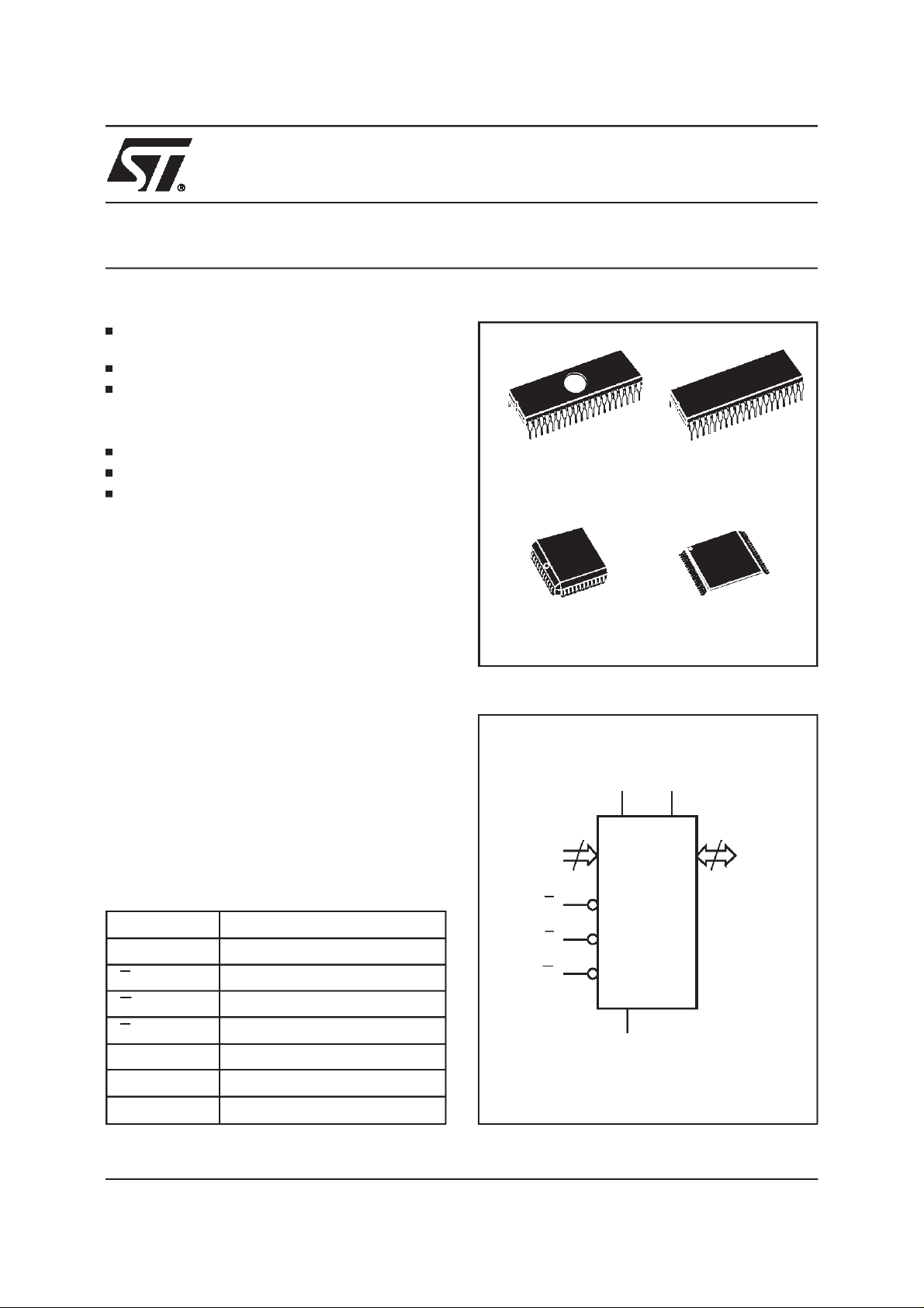
The FDIP40W(window ceramic frit-seal package)
has a transparent lid which allows the user to
expose the chip to ultraviolet light to erase the bit
pattern. A new pattern can then be written to the
deviceby following theprogramming procedure.
40
1
FDIP40W (F)
PLCC44 (K)
Figure1. Logic Diagram
V
16
A0-A15
CC
40
1
PDIP40 (B)
TSOP40 (N)
10 x 14mm
V
PP
16
Q0-Q15
Table 1. Signal Names
A0 - A15 Address Inputs
Q0 - Q15 Data Outputs
E Chip Enable
G Output Enable
P Program
V
PP
V
CC
V
SS
May 1998 1/15
Program Supply
Supply Voltage
Ground
P
E
G
M27V102
V
SS
AI01912
Page 2
M27V102
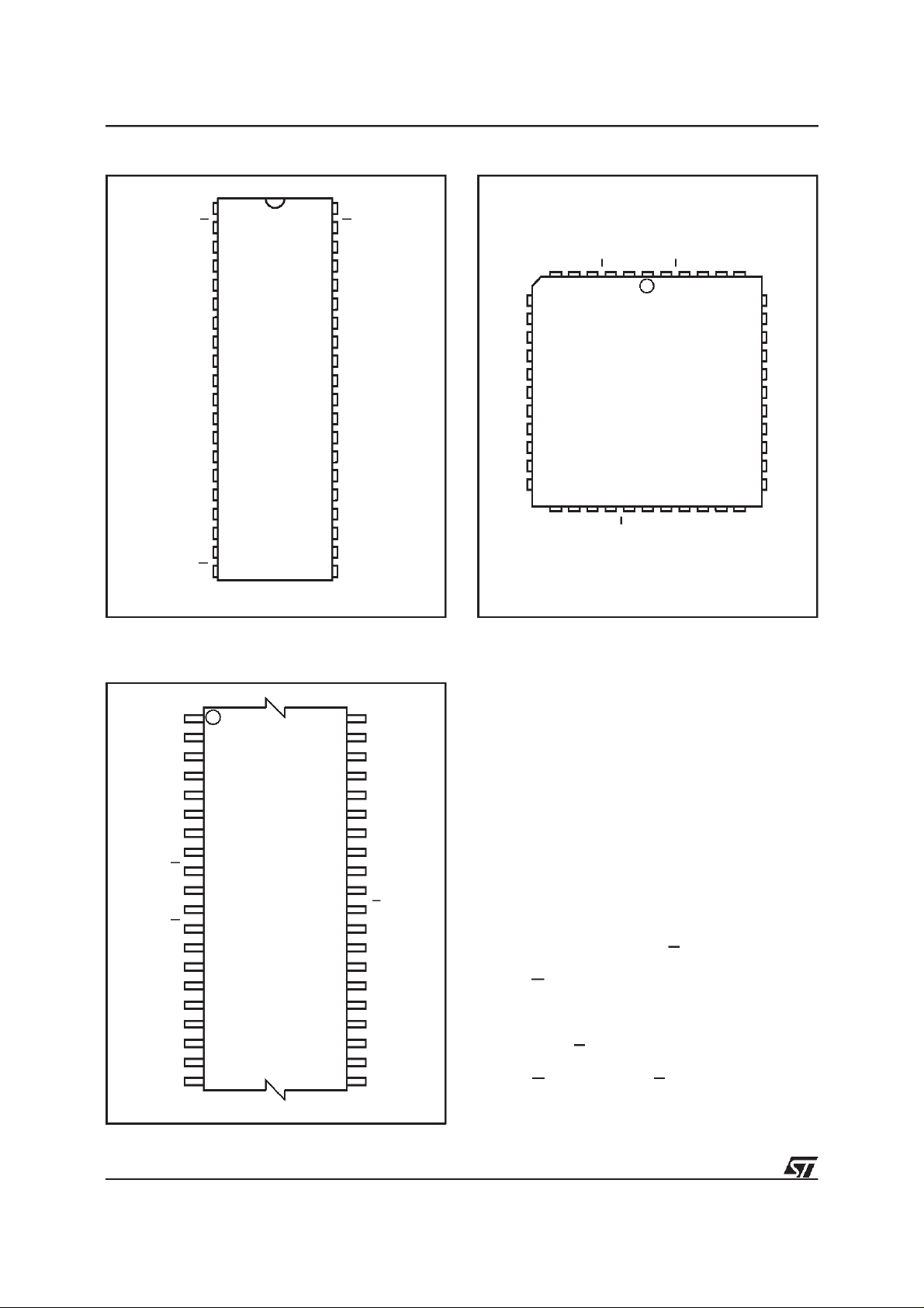
Figure2A. DIPPin Connections
V
PP
Q15
Q14
Q13
Q12
Q11
Q10
Q9
Q8
V
SS
Q7
Q6
Q5
Q4
Q3
Q2
Q0
1
2
3
4
5
6
7
8
9
10
11
12
13
14
15
16
17
18
19
M27V102
40
39
38
37
36
35
34
33
32
31
30
29
28
27
26
25
24
23
22
2120
AI01913
V
CC
PE
NC
A15
A14
A13
A12
A11
A10
A9
V
SS
A8
A7
A6
A5
A4
A3
A2Q1
A1
A0G
Figure2B. LCC Pin Connections
Q15
Q13
Q14
Q12
Q11
Q10
Q9 A10
Q8
V
SS
NC
Q6
Q5
Q4
12
Q3
Q2
Q1
Q0
M27V102
CC
NC
VPPE
V
44
1
23
G
A0
NC
P
A1
NC
A2
A15
A3
A14
34
A4
A13
A12
A11
A9
V
SS
NC
A8Q7
A7
A6
A5
AI01914
Warning: NC = Not Connected.
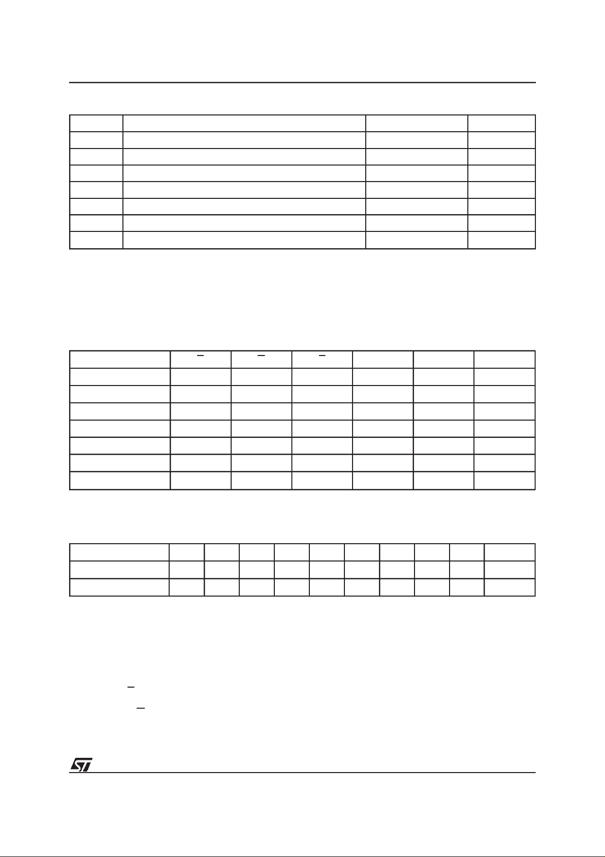
Figure2C. TSOPPin Connections
A9
1
A10
A11
A12 A6
A13 A5
A14
A15
NC
P
V
CC
V
DQ15
DQ14
DQ13
DQ12 DQ4
DQ11 DQ5
DQ10
DQ9
DQ8
Warning: NC = Not Connected.
10
11
PP
E
20 21
M27V102
(Normal)
40
31
30
AI01915
V
SS
A8
A7
A4
A3
A2
A1
A0
G
DQ0
DQ1
DQ2
DQ3
DQ6
DQ7
V
SS
Warning: NC = Not Connected.
DESCRIPTION
(cont’d)
For application where the content is programmed
only one time and erasure is not required, the
M27V102 is offered in PDIP40, PLCC32 and
TSOP40(10 x 14 mm) packages.
DEVICEOPERATION
Theoperating modes of the M27V102are listedin
theOperating Modestable. Asingle powersupply
is required in the read mode. All inputs are TTL
levelsexcept for Vpp and 12V onA9 for Electronic
Signature.
ReadMode
The M27V102 has two control functions, both of
whichmustbelogicallyactiveinordertoobtaindata
attheoutputs. ChipEnable(E) isthepowercontrol
and should be used for device selection. Output
Enable(G)isthe outputcontrolandshouldbe used
to gate data to the output pins, independent of
deviceselection. Assumingthatthe addressesare
stable,the addressaccesstime(t
thedelayfrom Etooutput(t
at the output after a delay of t
). Datais available
ELQV
OE
) is equal to
AVQV
from the falling
edge of G, assuming that E has been low and the
addresses have been stable for at least t
.
t
GLQV
AVQV
-
2/15
Page 3
M27V102
Table 2. Absolute MaximumRatings
(1)
Symbol Parameter Value Unit
T
A
T
BIAS
T
STG
V
IO
V
CC
V
A9
V
PP
Notes: 1. Except for therating ”Operating Temperature Range”, stresses above those listed in theTable ”AbsoluteMaximum Ratings”
2. Minimum DC voltage on Input or Output is –0.5V withpossible undershootto –2.0Vfor a periodless than 20ns. Maximum DC
3. Depends on range.
Ambient Operating Temperature
Temperature Under Bias –50 to 125
Storage Temperature –65 to 150 °C
(2)
Input or Output Voltages (except A9) –2 to 7 V
Supply Voltage –2 to 7 V
(2)
A9 Voltage –2 to 13.5 V
Program Supply Voltage –2 to 14 V
may cause permanent damage to thedevice. These are stress ratings only and operation of the device at these or any other
conditions above those indicatedin the Operating sections of this specification is not implied. Exposure to Absolute Maximum
Rating conditions for extendedperiods may affectdevice reliability.Refer also to the STMicroelectronics SURE Programand other
relevant qualitydocuments.
voltage on Output is V
+0.5Vwith possible overshoot to VCC+2V for a periodless than 20ns.
CC
(3)
–40 to 125 °C
°
C
Table 3. OperatingModes
Mode E G P A9 V
Read V
Output Disable V
Program V
Verify V
Program Inhibit V
Standby V
Electronic Signature V
Note: X=VIHor VIL,VID= 12V±0.5V
PP
IL
IL
IL
IL
IH
IH
IL
V
IL
V
IH
XV
V
IL
XXXVPPHi-Z
XXXV
V
IL
V
IH
XXV
Pulse X V
IL
V
IH
V
IH
XV
CC
CC
or V
or V
PP
SS
SS
XVPPData Output
or V
CC
SS
V
ID
V
CC
Q0 - Q15
Data Output
Hi-Z
Data Input
Hi-Z
Codes
Table 4. ElectronicSignature
Identifier A0 Q7 Q6 Q5 Q4 Q3 Q2 Q1 Q0 Hex Data
Manufacturer’s Code V
Device Code V
IL
IH
00100000 20h
10001100 8Ch
StandbyMode
TheM27V102hasastandbymode whichreduces
the active current from 15mA to 20µA with low
voltageoperationV
≤ 3.6V,see Read Mode DC
CC
Characteristics table for details. The M27V102 is
placedin thestandbymodeby applyinga TTLhigh
signal to the E input. When in the standby mode,
the outputs are in a high impedance state, independentof the G input.
Two Line Output Control
BecauseEPROMs areusuallyusedin largermemory arrays, this product features a 2 line control
functionwhich accommodatesthe use of multiple
memoryconnection. Thetwo line control function
allows:
a. the lowestpossible memory powerdissipation,
b. complete assurancethat outputbus contention
will not occur.
3/15
Page 4
M27V102
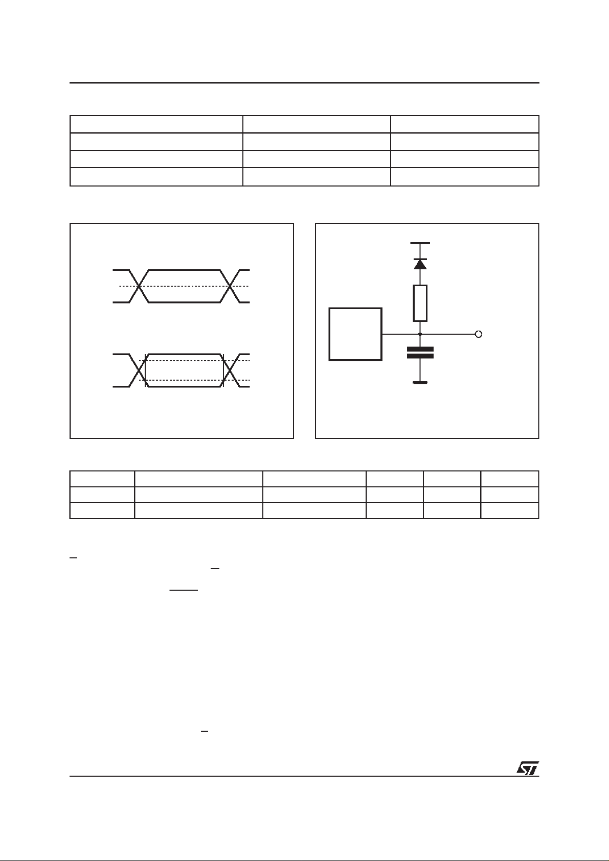
Table 5. AC MeasurementConditions
High Speed Standard
Input Rise and Fall Times
Input Pulse Voltages 0 to 3V 0.4V to 2.4V
Input and Output TimingRef. Voltages 1.5V 0.8V and 2V
≤
10ns
≤
20ns
Figure3. AC TestingInput Output Waveform
High Speed
3V
1.5V
0V
Standard
2.4V
0.4V
Table6. Capacitance
Symbol Parameter Test Condition Min Max Unit
C
IN
C
OUT
Note: 1. Sampled only, not 100% tested.
Input Capacitance VIN=0V 6 pF
Output Capacitance V
(1)
(TA=25°C, f = 1 MHz )
2.0V
0.8V
AI01822
Figure4. AC Testing LoadCircuit
1.3V
1N914
3.3kΩ
DEVICE
UNDER
TEST
C
L
CL= 30pF for High Speed
CL= 100pFfor Standard
CLincludes JIG capacitance
=0V 12 pF
OUT
OUT
AI01823B
Forthe mostefficientuseof thesetwocontrollines,
E should be decoded and used as the primary
deviceselecting function,while G shouldbe made
a common connection to all devices in the array
and connected to the READ line from the system
controlbus. Thisensuresthatall deselectedmemory devices are in their low power standby mode
and that the outputpinsare only active whendata
is requiredfrom a particularmemory device.
SystemConsiderations
The power switching characteristics of Advanced
CMOS EPROMsrequire carefuldecouplingof the
devices. The supply current, I
, has three seg-
CC
ments that are of interest to the system designer:
the standby current level, the active current level,
and transient current peaks that are produced by
thefallingand risingedgesof E. Themagnitudeof
4/15
transientcurrentpeaksisdependentonthe capacitive and inductive loading of the device at the
output.
The associated transient voltage peaks can be
suppressedby complying with the two line output
control and by properly selected decoupling capacitors. It is recommended thata 0.1µF ceramic
capacitor be used on every device between V
CC
andVSS. Thisshouldbea highfrequencycapacitor
of low inherent inductance and should be placed
as close to the device as possible. In addition, a
4.7µF bulk electrolytic capacitor should be used
betweenVcc and V
for everyeight devices.The
SS
bulk capacitor should be located near the power
supply connection point. The purpose of the bulk
capacitoris to overcome the voltage drop caused
by the inductiveeffectsof PCBtraces.
Page 5
M27V102
Table 7. Read Mode DC Characteristics
(1)
(TA=0 to 70 °C or –40 to 85 °C;VCC= 3.3V ± 10%; VPP=VCC)
Symbol Parameter TestCondition Min Max Unit
I
I
LO
I
CC
I
CC1
I
CC2
I
PP
V
V
IH
V
V
Notes: 1. VCCmust be applied simultaneously with or before VPPand removed simultaneously or after VPP.
Table 8A. Read ModeAC Characteristics
Input Leakage Current 0V ≤ VIN≤ V
LI
Output Leakage Current 0V ≤ V
,G=VIL,I
E=V
Supply Current
IL
f = 5MHz, V
Supply Current (Standby) TTL E = V
Supply Current (Standby)
CMOS
E>V
– 0.2V,V
CC
Program Current VPP=V
Input Low Voltage –0.3 0.8 V
IL
(2)
Input High Voltage 2 VCC+1 V
Output Low Voltage IOL= 2.1mA 0.4 V
OL
Output High VoltageTTL IOH= –400µA 2.4 V
OH
Output High Voltage CMOS I
2. Maximum DCvoltage on Output is V
CC
+0.5V
(1)
= –100µAV
OH
OUT
CC
≤ V
CC
= 0mA,
OUT
≤ 3.6V
CC
IH
3.6V 20
≤
CC
CC
– 0.7V V
CC
±10 µA
±10 µA
15 mA
1mA
10
(TA=0 to 70 °C or –40 to 85 °C;VCC= 3.3V ± 10%; VPP=VCC)
A
µ
A
µ
Symbol Alt Parameter Test Condition
-90
(3)
Min Max Min Max
t
t
AVQV
t
ELQV
t
GLQV
(2)
t
EHQZ
(2)
t
GHQZ
t
AXQX
Notes: 1. VCCmust be applied simultaneously with or before VPPand removed simultaneously with or afterV
2. Sampled only, not 100% tested.
3. Speed obtained with High Speed AC measurementconditions.
Address Valid to Output Valid E = VIL,G=V
ACC
tCEChip Enable Low to Output Valid G = V
tOEOutput Enable Low to Output Valid E = V
tDFChip Enable High to Output Hi-Z G = V
tDFOutput Enable Highto Output Hi-Z E = V
IL
IL
IL
IL
tOHAddress Transitionto Output Transition E = VIL,G=V
IL
IL
90 100 ns
90 100 ns
45 50 ns
0 30 0 30 ns
0 30 0 30 ns
00ns
M27V102
PP.
-100
Unit
5/15
Page 6

M27V102
Table 8B. Read ModeAC Characteristics
(1)
(TA=0 to 70 °C or –40 to 85 °C;VCC= 3.3V ± 10%; VPP=VCC)
M27V102
Symbol Alt Parameter Test Condition
-120 -150 -200
Min Max Min Max Min Max
t
AVQV
t
ELQV
t
GLQV
t
EHQZ
t
GHQZ
t
AXQX
Notes: 1. VCCmust be applied simultaneously with or before VPPand removed simultaneously with or afterV
t
Address Valid to Output Valid E = VIL,G=V
ACC
tCEChip Enable Low to OutputValid G = V
tOEOutput Enable Low to Output Valid E = V
(2)
tDFChip Enable High to Output Hi-Z G = V
(2)
tDFOutput Enable High to Output Hi-Z E = V
Address Transition to Output
t
OH
Transition
2. Sampled only, not 100% tested.
IL
IL
IL
IL
IL
E=V
,G=VIL000ns
IL
120 150 200 ns
120 150 200 ns
50 60 90 ns
040050070ns
040050070ns
Figure5. Read ModeAC Waveforms
A0-A15
tAVQV
VALID
tAXQX
VALID
Unit
PP.
E
tGLQV
G
tELQV
Q0-Q15
Programming
The M27V102has been designed to be fullycompatible with the M27C1024 and has the same
elecronicsignature.As a result the M27V102 can
be programmed as the M27C1024 on the same
programming equipmentsapplying12.75V on V
PP
and6.25Von VCCbythe useof thesamePRESTO
II algorithm. When delivered (and after each ’1’s
erasure for UV EPROM), all bits of the M27V102
arein the’1’state.Data isintroducedbyselectively
tEHQZ
tGHQZ
Hi-Z
AI00705B
programming ’0’s into the desired bit locations.
Although only ’0’s will be programmed, both ’1’s
and’0’s can bepresent in thedata word. The only
way to change a ’0’ to a ’1’ is by die exposure to
ultraviolet light (UV EPROM). The M27V102 is in
the programming mode when V
12.75V,E is at V
and P is pulsedto VIL. The data
IL
input is at
PP
to be programmed is applied to 16 bits in parallel
tothe data outputpins. Thelevels requiredfor the
addressand data inputs are TTL.V
to be 6.25V ±
0.25V.
is specified
CC
6/15
Page 7

M27V102
Table 9. ProgrammingMode DC Characteristics
(1)
(TA=25°C; VCC=6.25V ± 0.25V;VPP=12.75V ± 0.25V)
Symbol Parameter Test Condition Min Max Unit
I
LI
I
CC
I
PP
V
IL
V
IH
V
OL
V
OH
V
ID
Note: 1. VCCmust be applied simultaneously with or before VPPand removed simultaneously with or afterVPP.
Input Leakage Current 0≤V
Supply Current 50 mA
Program Current E = V
Input Low Voltage –0.3 0.8 V
Input High Voltage 2 VCC+ 0.5 V
Output Low Voltage IOL= 2.1mA 0.4 V
Output High VoltageTTL IOH= –400µA 2.4 V
A9 Voltage 11.5 12.5 V
Table 10. ProgrammingMode AC Characteristics
(1)
V
≤
IN
IH
IL
10
±
50 mA
(TA=25°C; VCC=6.25V ± 0.25V;VPP=12.75V ± 0.25V)
Symbol Alt Parameter Test Condition Min Max Unit
t
AVPL
t
AS
Address Validto Program Low 2 µs
A
µ
t
QVPL
t
VPHPL
t
VCHPL
t
ELPL
t
PLPH
t
PHQX
t
QXGL
t
GLQV
(2)
t
GHQZ
t
GHAX
Notes: 1. VCCmust be applied simultaneously with or before VPPand removed simultaneously with or afterVPP.
2. Sampled only, not 100% tested.
t
t
VPS
t
VCS
t
CES
t
t
t
OES
t
t
DFP
t
DS
PW
DH
OE
AH
Input Validto Program Low 2 µs
VPPHigh to ProgramLow 2 µs
VCCHigh to Program Low 2 µs
Chip Enable Low to Program Low 2 µs
Program Pulse Width 95 105 µs
Program High to Input Transition 2 µs
Input Transition to Output Enable
Low
2
Output EnableLow to Output Valid 100 ns
Output EnableHigh to Output Hi-Z 0 130 ns
Output EnableHigh to Address
Transition
0ns
s
µ
7/15
Page 8

M27V102
Figure6. Programmingand VerifyModes AC Waveforms
A0-A15
tAVPL
Q0-Q15
tQVPL
V
PP
tVPHPL
V
CC
tVCHPL
E
tELPL
P
tPLPH
G
Figure7. ProgrammingFlowchart
VCC= 6.25V, VPP= 12.75V
n=0
P = 100µs Pulse
NO
NO
VERIFY
YES
Last
NO
Addr
YES
CHECK ALLWORDS
1st: VCC=6V
2nd: VCC= 4.2V
++ Addr
YES
++n
=25
FAIL
VALID
DATA IN DATA OUT
tPHQX
tGLQV
tQXGL
PROGRAM VERIFY
PRESTOII ProgrammingAlgorithm
PRESTO II Programming Algorithm allows programming of the whole array with a guaranteed
margin,in a typical time of 6.5 seconds.Programming with PRESTO II consists of applying a sequenceof100µsprogrampulsestoeachworduntil
a correct verify occurs (see Figure 7). During programmingand verifyoperation,a MARGINMODE
circuitis automaticallyactivatedin orderto guarantee that each cell is programmed with enough
margin. No overprogrampulseis appliedsince the
verifyin MARGIN MODEat V
3.6V provides necessary margin to each programmedcell.
ProgramInhibit
ProgrammingofmultipleM27V102sin parallelwith
differentdata is also easily accomplished. Except
for E, all like inputs including G of the parallel
M27V102may be common. ATTLlow level pulse
appliedto aM27V102’sP input,withE lowand V
at12.75V,will programthat M27V102. Ahigh level
E input inhibits the other M27V102s from being
programmed.
ProgramVerify
AI00707C
A verify (read) should be performed on the programmedbits todeterminethattheywere correctly
programmed. The verify is accomplished with E
tGHQZ
tGHAX
AI00706
muchhigher than
CC
PP
8/15
Page 9

M27V102
and G at VIL, P at VIH,VPPat 12.75V and VCCat
6.25V.
On-BoardProgramming
The M27V102 can be directly programmed in the
application circuit. See the relevant Application
NoteAN620.
ElectronicSignature
The Electronic Signature (ES) mode allows the
reading outof a binarycode from an EPROMthat
will identify its manufacturer and type. This mode
is intended for use by programmingequipment to
automaticallymatchthe deviceto be programmed
withits correspondingprogrammingalgorithm.The
ES mode is functional in the 25°C± 5°Cambient
temperaturerange that is required whenprogramming the M27V102. To activatethe ES mode, the
programmingequipmentmustforce 11.5Vto 12.5V
onaddressline A9of the M27V102with V
PP=VCC
=5V. Twoidentifierbytes maythen besequenced
fromthedeviceoutputsby togglingaddresslineA0
fromV
at V
(A0=V
byte1 (A0=V
toVIH. Allotheraddresslinesmustbeheld
IL
during Electronic Signature mode. Byte 0
IL
) represents the manufacturer code and
IL
) the deviceidentifiercode. For the
IH
STMicroelectronicsM27V102,thesetwo iden-tifier
bytes are givenin Table4 and can be read-out on
outputs Q0 to Q7. Note that the M27V102 and
M27C1024have the same identifier bytes.
ERASUREOPERATION (appliesto UVEPROM)
Theerasurecharacteristicsof theM27V102issuch
that erasurebegins when the cells areexposed to
light with wavelengths shorter than approximately
4000Å. It shouldbe noted thatsunlight and some
type offluorescentlamps have wavelengthsin the
3000-4000Årange.Researchshowsthat constant
exposure to room level fluorescent lighting could
erasea typical M27V102in about 3 years, whileit
wouldtakeapproximately1 weekto causeerasure
when exposed to direct sunlight. If the M27V102
is to be exposed to these types of lighting conditions for extended periodsof time, it is suggested
that opaque labels be put over the M27V102 window to preventunintentionalerasure. The recommended erasure procedure for the M27V102 is
exposure to short wave ultraviolet light which has
wavelength2537 Å. The integrated dose (i.e. UV
intensityx exposuretime) for erasure should be a
minimumof 15 W-sec/cm
this dosage is approximately 15 to 20 minutes
usingan ultravioletlampwith12000µW/cm
2
. The erasuretime with
2
power
rating. The M27V102should be placed within 2.5
cm (1 inch) of the lamp tubes during the erasure.
Some lamps have a filter on their tubes which
shouldbe removed beforeerasure.
9/15
Page 10

M27V102
ORDERING INFORMATION SCHEME
Example: M27V102 -90 K 1 TR
Speed
(1)
-90
-100 100 ns
-120 120 ns
-150 150 ns
-200 200 ns
Note: 1. High Speed, see AC Characteristicssection for furtherinformation.
90 ns
Package
F FDIP40W
B PDIP40
K PLCC44
N TSOP40
8 x 14mm
Temperature Range
1 0 to 70 °C
6 –40 to 85°C
Option
TR Tape& Reel
Packing
Fora listofavailableoptions(Speed,Package,etc...)or forfurtherinformationon anyaspectofthisdevice,
pleasecontact the STMicroelectronics Sales Officenearest to you.
10/15
Page 11

FDIP40W - 40 pin Ceramic Frit-seal DIP, with window
M27V102
Symb
A 5.72 0.225
A1 0.51 1.40 0.020 0.055
A2 3.91 4.57 0.154 0.180
A3 3.89 4.50 0.153 0.177
B 0.41 0.56 0.016 0.022
B1 1.45 – – 0.057 – –
C 0.23 0.30 0.009 0.012
D 51.79 52.60 2.039 2.071
D2 48.26 – – 1.900 – –
E 15.24 – – 0.600 – –
E1 13.06 13.36 0.514 0.526
e 2.54 – – 0.100 – –
eA 14.99 – – 0.590 – –
eB 16.18 18.03 0.637 0.710
L 3.18 0.125
S 1.52 2.49 0.060 0.098
∅
α
N40 40
Typ Min Max Typ Min Max
7.62 – – 0.300 – –
mm inches
4
°
11
°
4
°
11
°
Drawing is notto scale.
A2
B1 B e
D2
D
S
N
1
A3A1A
L
α
C
eA
eB
∅
E1 E
FDIPW-a
11/15
Page 12

M27V102
PDIP40 - 40 pin Plastic DIP, 600 mils body width
Symb
Typ Min Max Typ Min Max
A 4.45 – – 0.175 – –
A1 0.64 0.38 – 0.025 0.015 –
A2 3.56 3.91 0.140 0.154
B 0.38 0.53 0.015 0.021
B1 1.14 1.78 0.045 0.070
C 0.20 0.31 0.008 0.012
D 51.78 52.58 2.039 2.070
D2 48.26 – – 1.900 – –
E 14.80 16.26 0.583 0.640
E1 13.46 13.99 0.530 0.551
e1 2.54 – – 0.100 – –
eA 15.24 – – 0.600 –
eB 15.24 17.78 0.600 0.700
L 3.05 3.81 0.120 0.150
S 1.52 2.29 0.060 0.090
α
N40 40
mm inches
0
°
15
°
0
°
15É
Drawing is notto scale.
12/15
B1 B e1
D2
D
S
N
1
A2A1A
E1 E
L
α
C
eA
eB
PDIP
Page 13

PLCC44 - 44 lead Plastic Leaded Chip Carrier, square
M27V102
Symb
Typ Min Max Typ Min Max
A 4.20 4.70 0.165 0.185
A1 2.29 3.04 0.090 0.120
A2 – 0.51 – 0.020
B 0.33 0.53 0.013 0.021
B1 0.66 0.81 0.026 0.032
D 17.40 17.65 0.685 0.695
D1 16.51 16.66 0.650 0.656
D2 14.99 16.00 0.590 0.630
E 17.40 17.65 0.685 0.695
E1 16.51 16.66 0.650 0.656
E2 14.99 16.00 0.590 0.630
e 1.27 – – 0.050 – –
F 0.00 0.25 0.000 0.010
R 0.89 – – 0.035 – –
N44 44
CP 0.10 0.004
mm inches
D
D1
1N
Ne E1 E
Nd
PLCC
Drawing is notto scale.
R
F
0.51 (.020)
1.14 (.045)
D2/E2
A1
A2
B1
e
B
A
CP
13/15
Page 14

M27V102
TSOP40- 40 lead Plastic Thin Small Outline, 10 x 14mm
Symb
Typ Min Max Typ Min Max
A 1.20 0.047
A1 0.05 0.15 0.002 0.006
A2 0.95 1.05 0.037 0.041
B 0.17 0.27 0.007 0.011
C 0.10 0.21 0.004 0.008
D 13.80 14.20 0.543 0.559
D1 12.30 12.50 0.484 0.492
E 9.90 10.10 0.390 0.398
e 0.50 – – 0.020 – –
L 0.50 0.70 0.020 0.028
α
N40 40
CP 0.10 0.004
mm inches
0
°
5
°
0
°
5
°
Drawing is notto scale.
1N
E
N/2
D1
D
DIE
TSOP-a
A2
e
B
A
CP
C
LA1 α
14/15
Page 15

M27V102
Information furnished is believed to be accurate and reliable. However, STMicroelectronics assumes no responsibility for the consequences
ofuse ofsuch information nor for any infringement of patents or other rights of third parties which may resultfrom its use. Nolicense is granted
by implicationor otherwise under any patent or patent rights of STMicroelectronics. Specifications mentioned in thispublicationare subject to
change without notice. This publication supersedes and replaces all information previously supplied. STMicroelectronics products are not
authorized for use as critical components in life support devices or systems without express writtenapproval of STMicroelectronics.
The ST logois a registeredtrademark of STMicroelectronics.
1998 STMicroelectronics - AllRights Reserved
Australia - Brazil - Canada - China - France- Germany- Italy- Japan -Korea - Malaysia - Malta- Morocco - The Netherlands - Singapore -
Spain - Sweden - Switzerland - Taiwan- Thailand - United Kingdom -U.S.A.
STMicroelectronics GROUP OF COMPANIES
15/15
 Loading...