

Page 1
64 Kbit (8Kb x 8) UV EPROM and OTP EPROM
5V ± 10% SUPPLY VOLTAGE in READ
OPERATION
FAST A CCES S TIME : 150ns
LOW POWER “CMOS” CONSUMPTION:
– Active Current 30mA
– Standby Current 100µA
PROGRAMMING VOLT AGE: 12.5V ± 0.25V
HIGH SP EED PROGRAMMING
(less than 1 minute)
ELECTRONIC SIGNATURE
– Manufacturer Code: 9Bh
– Device Code: 08h
DESCRIPTION
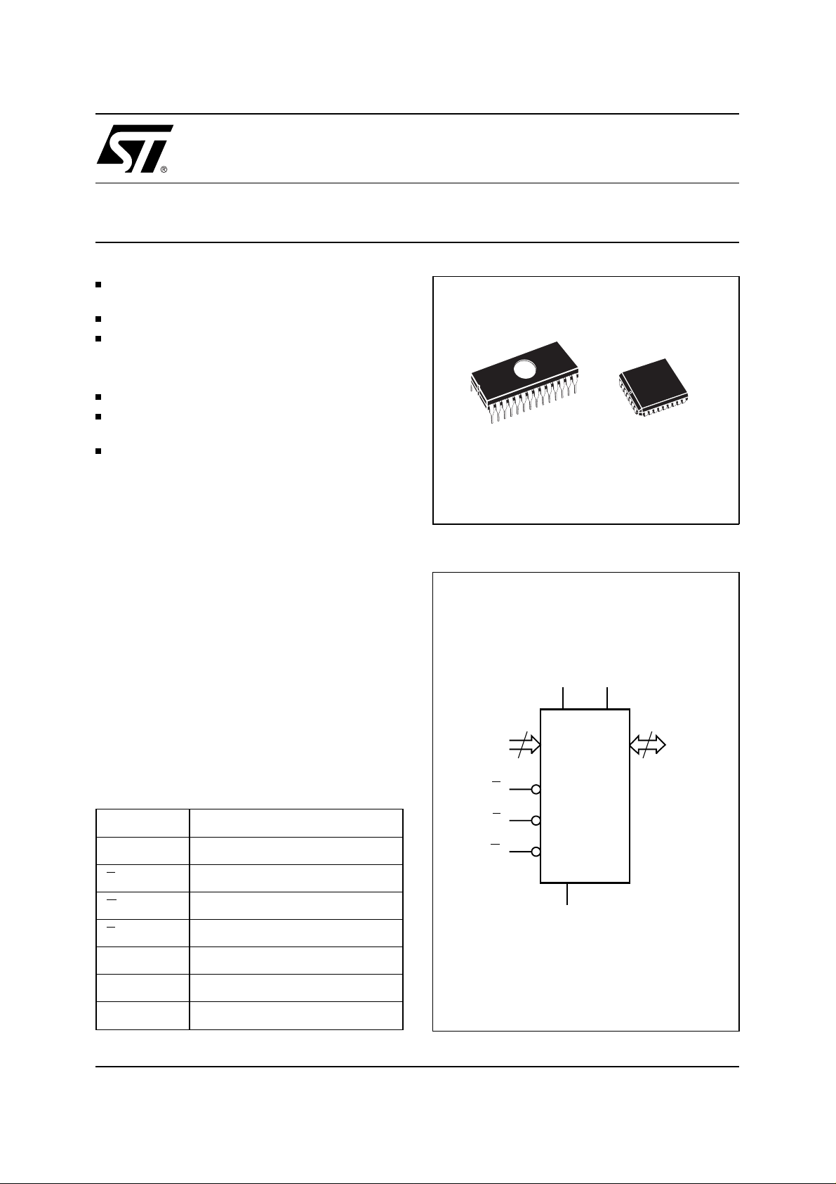
The M27C64A is a 64Kbit EPROM offered in the
two ranges UV (ultra violet erase) and OTP (one
time programmable). It is ideally suited for microprocessor systems requiring large programs and is
organized as 8,192 by 8 bits.
The FDIP28W (window ceramic frit-seal package)
has transparent lid which allows the user to expose
the chip to ultraviolet light to erase the bit pattern.
A new pattern can then be written to the device by
following the programming procedure.
For applications where the content is programmed
only on time and erasure is not required, the
M27C64A is offered in PLCC32 package.
28
1
FDIP28W (F)
Figure 1. Logic Diagram
V
CC
13
A0-A12
M27C64A
PLCC32 (C)
V
PP
8
Q0-Q7
T ab le 1. Signal Names
A0-A12 Address Inputs
Q0-Q7 Data Outputs
E Chip Enable
G Output Enable
P Program
V
PP
V
CC
V
SS
March 1998 1/12
Program Supply
Supply Voltage
Ground
P
E
G
M27C64A
V
SS
AI00834B
Page 2
M27C64A
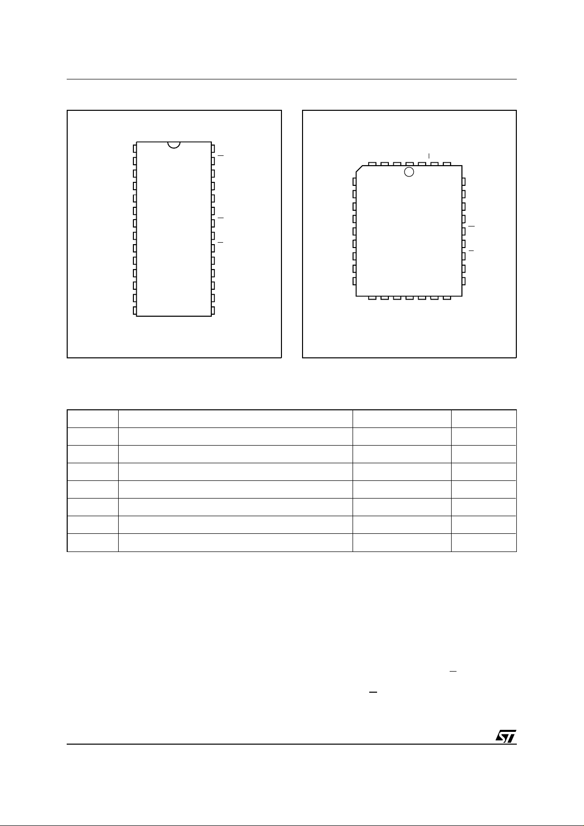
Figure 2A. DIP Pin Connections
V
Warning:
1
PP
2
A7
3
4
A6
5
A5
A4
6
7
A3
A2
A1
A0
Q0
Q1
Q2
V
SS
NC = Not Connected
M27C64A
8
9
10
11
12
13
14
28
27
26
25
24
23
22
21
20
19
18
17
16
15
AI00835
V
CC
PA12
NC
A8
A9
A11
G
A10
E
Q7
Q6
Q5
Q4
Q3
Figure 2B. LCC Pin Connections
PP
CC
DU
32
DU
V
Q3
P
Q4
Warning:
V
A7
A12
1
A6
A5
A4
A3
A2
9
M27C64A
A1
A0
NC
Q0
17
Q1
Q2
SS
V
NC = Not Connected, DU = Don’t Use
NC
25
Q5
A8
A9
A11
NC
G
A10
E
Q7
Q6
AI00836
(1)
T ab le 2. Absolute Maximum Ratings
Symbol Parameter Value Unit
T
A
T
BIAS
T
STG
(2)
V
IO
V
CC
(2)
V
A9
V
PP
Notes:
1. Except for the rating "Operating Temperature Range", stresses above those listed in the Table "Absolute Maximum Ratings"
2. Minimum DC voltage on Input or Output is –0.5V with possible undershoot to –2.0V for a period less than 20ns. Maximum DC
3. Depends on range.
Ambient Operating Temperature
Temperature Under Bias –50 to 125 °C
Storage Temperature –65 to 150 °C
Input or Output Voltages (except A9) –2 to 7 V
Supply Voltage –2 to 7 V
A9 Voltage –2 to 13.5 V
Program Supply Voltage –2 to 14 V
may cause permanent damage to the device. These are stress rating s only and operation of the device at these or any other
conditions above those indicated in the Operating sections of this specification is not implied. Exposure to Absolute Maximum
Rating conditions for extended periods may affect device reliability. Refer also to the STMicroelectronics SURE Program and other
relevant quality documents.
voltage on Output is V
+0.5V with possible overshoot to VCC +2V for a period less than 20ns.
CC
DEVICE O PERATION
The modes of operation of the M27C64A are listed
in the Operating Modes table. A single power supply is required in the read mode. All inputs are TTL
levels except for V
and 12V on A9 for Electronic
PP
Signature.
(3)
–40 to 125 °C
Read Mode
The M27C64A has two control functions, both of
which must be logically active in order to obtain
data at the outputs. Chip Enable (
E) is the power
control and should be used for device selection.
Output Enable (
G) is the output control and should
2/12
Page 3
M27C64A
be used to gate data to the output pins, independent of device selection. Assuming that the
addresses are stable, the address access time
) is equal to the delay from E to output (t
(t
AV QV
Data is available at the output after a delay of t
ELQV
GLQV
from the falling edge of G, assuming that E has
been low and the addresses have been stable for
at least t
AVQV-tGLQV
.
Standby Mode
The M27C64A has a standby mode which reduces
the active current from 30mA to 100µA. The
M27C64A is placed in the standby mode by applying a CMOS high signal to the
E input. When in the
standby mode, the outputs are in a high impedance
state, independent of the
G input.
T wo Line Output Control
Because EPROMs are usually used in larger memory arrays, this product features a 2 line control
function which accommodates the use of multiple
memory connection. The two line control function
allows:
a. the lowest possible memory power dissipation,
b. complete assurance that output bus contention
will not occur.
For the most efficient use of these two control lines,
E should be decoded and used as the primary
device selecting function, while
G should be made
a common connection to all devices in the array
and connected to the
READ line from the system
control bus. This ensures that all deselected memory devices are in their low power standby mode
and that the output pins are only active when data
).
is required from a particular memory device.
System Considerations
The power switching characteristics of Advanced
CMOS EPROMs require careful decoupling of the
devices. The supply current, I
, has three seg-
CC
ments that are of interest to the system designer:
the standby current level, the active c urrent level,
and transient current peaks that are produced by
the falling and rising edges of
E. The magnitude of
the transient current peaks is dependent on the
capacitive and inductive loading of the device at the
output.
The associated transient voltage peaks can be
suppressed by complying with the two line output
control and by properly selected decoupling capacitors. It is recommended that a 0.1µF ceramic
capacitor be used on every device between V
and VSS. This should be a high frequency capacitor
of low inherent inductance and should be placed
as close to the device as possible. I n addition, a
4.7µF bulk electrolytic capacitor should be used
between V
and VSS for every eight devices. T he
CC
bulk capacitor should be located near the power
supply connection point. The purpose of the bulk
capacitor is to overcome the voltage drop caused
by the inductive effects of PCB traces.
CC
T ab le 3. Operating Modes
Mode E G PA9VPPQ0 - Q7
Read V
Output Disable V
Program V
Verify V
Program Inhibit V
Standby V
Electronic Signature V
Note
: X = V
or VIL, VID = 12V ± 0.5V
IH
IL
IL
IL
IL
IH
IH
IL
V
IL
V
IH
V
IH
V
IL
XXXVPPHi-Z
XXXVCCHi-Z
V
IL
V
IH
V
IH
VIL Pulse X V
V
IH
V
IH
XVCCData Out
XVCCHi-Z
XVPPData Out
V
ID
PP
V
CC
T able 4. Electronic Signature
Identifier A0 Q7 Q6 Q5 Q4 Q3 Q2 Q1 Q0 Hex Data
Manufacturer’s Code V
Device Code V
IL
IH
10011011 9Bh
00001000 08h
Data In
Codes
3/12
Page 4

M27C64A
Programming
When delivered (and after each erasure for UV
EPROM), all bits of the M27C64A are in the "1"
state. Data is introduced by selectively programming "0"s into the desired bit locations. Although
only "0"s will be programmed, both "1"s and "0"s
can be present in the dat a word. The only way to
change a "0" to a "1" is by die exposition to ultraviolet light (UV EPROM). The M27C64A is in the
programming mode when V
is at V
and P is pulsed to VIL. The data to be
IL
input is at 12.5V, E
pp
programmed is applied to 8 bits in parallel to the
data output pins. The levels required for the address and data inputs are TTL. V
is specified to
CC
be 6V ± 0.25V .
High Speed Programming
The high speed programming algorithm, described
in the flowchart, rapidly programs the M27C64A
using an efficient and reliable method, part icularly
suited to the production programming environment. An individual device will take around 1 minute
to program.
Program Inhibit
Programming of multiple M27C64A in parallel with
different data is also easily accomplished. Except
E, all like inputs including G of the parallel
for
M27C64A may be common. A TTL low level pulse
applied to a M27C64A
P input, with E low and V
PP
at 12.5V, will program that M27C64A. A high level
E input inhibits the other M27C64A from being
programmed.
Program Verify
A verify (read) should be performed on the programmed bits to determine that they were correctly
programmed. The verify is accomplished with
G at VIL, P at VIH, VPP at 12.5V and VCC at 6V.
and
Electronic Signature
The Electronic Signature (ES) mode allows the
reading out of a binary code from an EPROM that
will identify its manufacturer and type. This mode
is intended for use by programming equipment to
automatically match the device to be programmed
with its corresponding programming algorithm. The
ES mode is functional in the 25°C ± 5°C ambient
temperature range that is required when programming the M27C64A. To activate the ES mode, the
programming equipment must force 1 1.5V to 12.5V
on address line A9 of the M27C64A, with
V
PP=VCC
=5V. Two identifier bytes may then be
sequenced from the device outputs by toggling
address line A0 from V
lines must be held at V
to VIH. All other address
IL
during Electronic Signa-
IL
ture mode.
Byte 0 (A0=V
and byte 1 (A0=V
) represents the manufacturer code
IL
) the device identifier code. For
IH
the STMicroelectronics M27C64A, these two identifier bytes are given in Table 4 and can be read-out
on outputs Q0 to Q7.
E
4/12
Page 5

M27C64A
AC MEASUREMENT CONDITIONS
Figure 4. AC Testing Load Circuit
Input Rise and Fall Times ≤ 20ns
Input Pulse Voltages 0.4V to 2.4V
Input and Output Timing Ref.
Voltages
0.8V to 2.0V
1.3V
1N914
Note that Output Hi-Z is defined as the point where data
is no longer driven.
Figure 3. AC Testing Input O utput Waveforms
2.4V
0.4V
T ab le 5. Capacitance
(1)
(TA = 25 °C, f = 1 MHz )
2.0V
0.8V
AI00826
DEVICE
UNDER
TEST
CL includes JIG capacitance
3.3kΩ
CL = 100pF
Symbol Parameter Test Condition Min Max Unit
C
IN
C
OUT
Note:
1. Sampled only, not 100% tested.
Input Capacitance VIN = 0V 6 pF
Output Capacitance V
= 0V 12 pF
OUT
OUT
AI00828
Figure 5. Read Mode AC Waveforms
A0-A12
tAVQV
E
G
tELQV
Q0-Q7
VALID
tGLQV
VALID
tAXQX
tEHQZ
tGHQZ
Hi-Z
AI00778B
5/12
Page 6

M27C64A
Table 6. Read Mode DC Characteristics
(1)
(TA = 0 to 70 °C or –40 to 85 °C: VCC = 5V ± 10%; VPP = VCC)
Symbol Parameter Test Condition Min Max Unit
I
I
I
CC
I
CC1
I
CC2
I
V
VIH
V
V
Notes:
Input Leakage Current 0V ≤ VIN ≤ V
LI
Output Leakage Current 0V ≤ V
LO
Supply Current
Supply Current (Standby) TTL E = V
E = VIL, G = VIL,
= 0mA, f = 5MHz
I
OUT
OUT
≤ V
IH
CC
CC
Supply Current (Standby) CMOS E > VCC – 0.2V 100 µA
Program Current VPP = V
PP
Input Low Voltage –0.3 0.8 V
IL
(2)
Input High Voltage 2 VCC + 1 V
Output Low Voltage IOL = 2.1mA 0.4 V
OL
Output High Voltage TTL IOH = –400µA 2.4 V
OH
Output High Voltage CMOS IOH = –100µAV
1. V
must be applied simultaneously with or before VPP and removed simultaneously with or after V
CC
2. Maximum DC voltage on Output is V
CC
+0.5V .
CC
– 0.7V V
CC
PP .
±10 µA
±10 µA
30 mA
1mA
100 µA
Table 7. Read Mode AC Characteristics
(1)
(TA = 0 to 70 °C or –40 to 85 °C: VCC = 5V ± 10%; VPP = VCC)
Symbol Alt Parameter Test Condition
t
AVQV
t
ELQV
t
GLQV
(2)
t
EHQZ
(2)
t
GHQZ
t
AXQX
Notes:
1. V
must be applied simultaneously with or before VPP and removed simultaneously with or after V
CC
2. Sampl ed only, not 100% tested.
Address Valid to
t
ACC
Output Valid
Chip Enable Low to
t
CE
Output Valid
Output Enable Low
t
OE
to Output Valid
Chip Enable High to
t
DF
Output Hi-Z
Output Enable High
t
DF
to Output Hi-Z
Address Transition to
t
OH
Output Transition
E = VIL, G = V
G = V
E = V
G = V
E = V
E = VIL, G = VIL0000ns
IL
IL
IL
IL
-15 -20 -25 -30
Min Max Min Max Min Max Min Max
IL
0500500600105ns
0500500600105ns
M27C64A
Unit
150 200 250 300 ns
150 200 250 300 ns
75 80 100 120 ns
PP.
6/12
Page 7

M27C64A
T ab le 8. Programming Mode DC Characteristics
(1)
(TA = 25 °C; VCC = 6V ± 0.25V; VPP = 12.5V ± 0.25V)
Symbol Parameter Test Condition Min Max Unit
I
LI
I
CC
I
PP
V
IL
V
IH
V
OL
V
OH
V
ID
Note:
1. V
CC
T ab le 9. Programming Mode AC Characteristics
Input Leakage Current VIL ≤ VIN ≤ V
IH
±10 µA
Supply Current 30 mA
Program Current E = V
IL
30 mA
Input Low Voltage –0.3 0.8 V
Input High Voltage 2 VCC + 0.5 V
Output Low Voltage IOL = 2.1mA 0.4 V
Output High Voltage TTL IOH = –400µA 2.4 V
A9 Voltage 11.5 12.5 V
must be applied simultaneousl y with or before VPP and removed simultaneously or after VPP.
(1)
(TA = 25 °C; VCC = 6V ± 0.25V; VPP = 12.5V ± 0.25V)
Symbol Alt Parameter Test Condition Min Max Unit
t
AVPL
t
QVPL
t
VPHPL
t
VCHPL
t
ELPL
t
PLPH
t
PHQX
t
QXGL
t
GLQV
t
GHQZ
t
GHAX
Notes:
1. V
2. Sampled only, not 100% tested.
t
t
t
VPS
t
VCS
t
CES
Address Valid to Program Low 2 µs
AS
Input Valid to Program Low 2 µs
DS
VPP High to Program Low 2 µs
VCC High to Program Low 2 µs
Chip Enable Low to
Program Low
Program Pulse Width (Initial) 0.95 1.05 ms
t
PW
Program Pulse Width (Over
Program)
t
t
OES
t
(2)
t
DFP
t
must be applied simultaneousl y with or before VPP and removed simultaneously or after V
CC
Program High to Input
DH
Transition
Input Transition to Output
Enable Low
Output Enable Low to
OE
Output Valid
Output Enable High to
Output Hi-Z
Output Enable High to
AH
Address Transition
2 µs
2.85 78.75 ms
2 µs
2 µs
100 ns
0 130 ns
0ns
PP.
7/12
Page 8

M27C64A
Figure 6. Programming and Verify Modes AC Waveforms
A0-A12
tAVPL
Q0-Q7
V
PP
V
CC
E
P
G
DATA IN DATA OUT
tQVPL
tVPHPL
tVCHPL
tELPL
tPLPH
Figure 7. Programming Flowchart
VCC = 6V, VPP = 12.5V
n = 1
P = 1ms Pulse
NO
NO
VERIFY
YES
P = 3ms Pulse by n
Last
NO
Addr
YES
CHECK ALL BYTES
1st: VCC = 6V
2nd: VCC = 4.2V
++ Addr
YES
++n
> 25
FAIL
VALID
tPHQX
tGLQV
tQXGL
PROGRAM VERIFY
ERASURE OP ERA TI ON (applies to UV EPRO M)
The erasure characteristics of the M27C64A is
such that erasure begins when the cells are exposed to light with wavelengths shorter than approximately 4000 Å. It should be noted that sunlight
and some type of f luorescent lamps have wavelengths in the 3000-4000 Å range. Research
shows that constant exposure to room level fluorescent lighting could erase a typical M27C64A in
about 3 years, while it would take approximately 1
week to cause erasure when exposed to direct
sunlight. If the M27C64A is to be exposed to these
types of lighting conditions for extended periods of
time, it is suggested that opaque labels be put over
the M27C64A window t o prevent unintentional erasure. The recommended erasure procedure for
the M27C64A is exposure to short wave ultraviolet
light which has a wavelength of 2537 Å. The integrated dose (i.e. UV intensity x exposure time) for
erasure should be a minimum of 15 W-sec/cm
The erasure time with this dosage is approximately
15 to 20 minutes using an ultraviolet lamp with
12000 µW/cm
be placed within 2.5 cm (1 inch) of the lamp tubes
during the erasure. Some lamps have a filter on
their tubes which should be removed before erasure.
AI01167
tGHQZ
tGHAX
AI00779
2
power rating. The M27C64A s hould
2
.
8/12
Page 9

ORDERING INFORMATION SCHEME
Example: M27C64A -15 C 1 TR
M27C64A
Speed
-15 150 ns
-20 200 ns
-25 250 ns
-30 300 ns
Package
F FDIP28W
C PLCC32
Temperature Range
1 0 to 70 °C
6 –40 to 85 °C
Option
X Additional
Burn-in
TR Tape & Reel
Packing
For a list of available options (Speed, Package, etc...) refer to the current Memory Shortform catalogue.
For further information on any aspect of this device, please contact the STMicroelectronics Sales Office
nearest to you.
9/12
Page 10

M27C64A
FDIP28W - 28 pin Ceramic Frit-seal DIP, with window
Symb
Typ Min Max Typ Min Max
A 5.72 0.225
A1 0.51 1.40 0.020 0.055
A2 3.91 4.57 0.154 0.180
A3 3.89 4.50 0.153 0.177
B 0.41 0.56 0.016 0.022
B1 1.45 – – 0.057 – –
C 0.23 0.30 0.009 0.012
D 36.50 37.34 1.437 1.470
D2 33.02 – – 1.300 – –
E 15.24 – – 0.600 – –
E1 13.06 13.36 0.514 0.526
e2.54– –0.100– –
eA 14.99 – – 0.590 – –
eB 16.18 18.03 0.637 0.710
L 3.18 0.125
S 1.52 2.49 0.060 0.098
∅ 8.89 – – 0.350 – –
α 4° 11° 4° 11°
N28 28
mm inches
Drawing is no to scale
10/12
A2
B1 B e
D2
D
S
N
1
∅
A3
A1AL
E1 E
α
C
eA
eB
FDIPW-a
Page 11

PLCC32 - 32 lead Plastic Leaded Chip Carrier - rect angular
M27C64A
Symb
Typ Min Max Typ Min Max
A 2.54 3.56 0.100 0.140
A1 1.52 2.41 0.060 0.095
A2 – 0.38 – 0.015
B 0.33 0.53 0.013 0.021
B1 0.66 0.81 0.026 0.032
D 12.32 12.57 0.485 0.495
D1 11.35 11.56 0.447 0.455
D2 9.91 10.92 0.390 0.430
E 14.86 15.11 0.585 0.595
E1 13.89 14.10 0.547 0.555
E2 12.45 13.46 0.490 0.530
e1.27– –0.050– –
F 0.00 0.25 0.000 0.010
R 0.89 – – 0.035 – –
N32 32
Nd 7 7
Ne 9 9
CP 0.10 0.004
mm inches
D
D1
1 N
Ne E1 E
Nd
PLCC
Drawing is no to scale
R
F
0.51 (.020)
1.14 (.045)
D2/E2
A1
A2
B1
e
B
A
CP
11/12
Page 12

M27C64A
Information furnished is believ ed to be accura te a nd rel i abl e. However, STMicroelec tronics assumes no responsibility for the consequences
of use of such information nor for any infringement of patents or other rights of third parties which may result from its use. No license is granted
by implication or otherwise under any patent or patent rights of STMicroelectronics. Specifications mentioned in this publication are subject to
change without notice. This publication supersedes and repl aces all information previously supplied. STMicroelectron ics products are not
authorized for use as critical components in life support devices or systems without express written approval of STMicroelectronics.
The ST logo is a registered trademark of STMicroelect roni cs
© 1998 STMicroelectronics - All Rights Reserved
Australia - Brazil - Canada - China - France - Germany - Italy - Japan - Korea - Malaysia - Malta - Mexico - Morocco - The Netherlands -
Singapore - Spain - Sweden - Switzerland - Taiwan - Thailand - United Kingdom - U.S.A.
STMicroelectronics GROUP OF COMPANIES
12/12
 Loading...