

Page 1
5V ± 10% SUPPLYVOLTAGEin READ
OPERATION
FASTACCESSTIME: 35ns
LOW POWERCONSUMPTION:
– ActiveCurrent 30mAat 5MHz
– Stand-byCurrent 100µA
PROGRAMMINGVOLTAGE:12.75V±0.25V
PROGRAMMINGTIME: 100µs/word (typical)
ELECTRONICSIGNATURE
– ManufacturerCode:0020h
– DeviceCode: 000Fh
DESCRIPTION
TheM27C516 is a 512Kbit EPROM offeredin the
OTP range (one time programmable). It is ideally
suited for microprocessorsystems requiring large
data or program storage and is organized as
32,768 words of 16 bits.
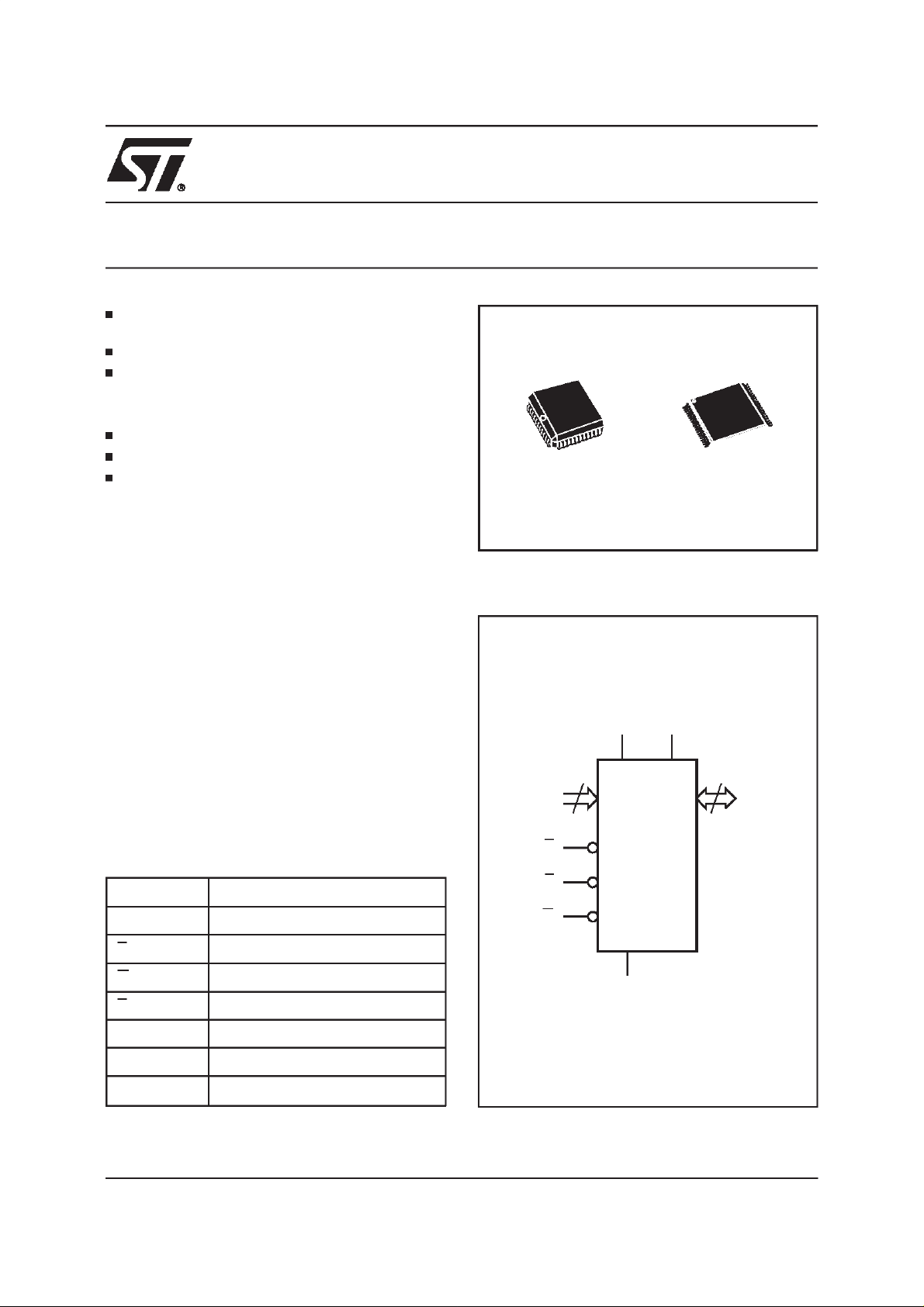
TheM27C516isofferedin aPLCC44andTSOP40
(10 x 14mm)packages.
M27C516
512 Kbit (32Kb x16) OTP EPROM
PLCC44 (C) TSOP40 (N)
Figure1. LogicDiagram
V
CC
15
A0-A14
V
PP
10 x 14mm
16
Q0-Q15
P
Table1. SignalNames
A0-A14 Address Inputs
Q0-Q15 Data Outputs
E Chip Enable
G Output Enable
P Program Enable
V
CC
V
PP
V
SS
September 1998 1/12
Supply Voltage
Program Supply
Ground
E
G
M27C516
V
SS
AI00932
Page 2
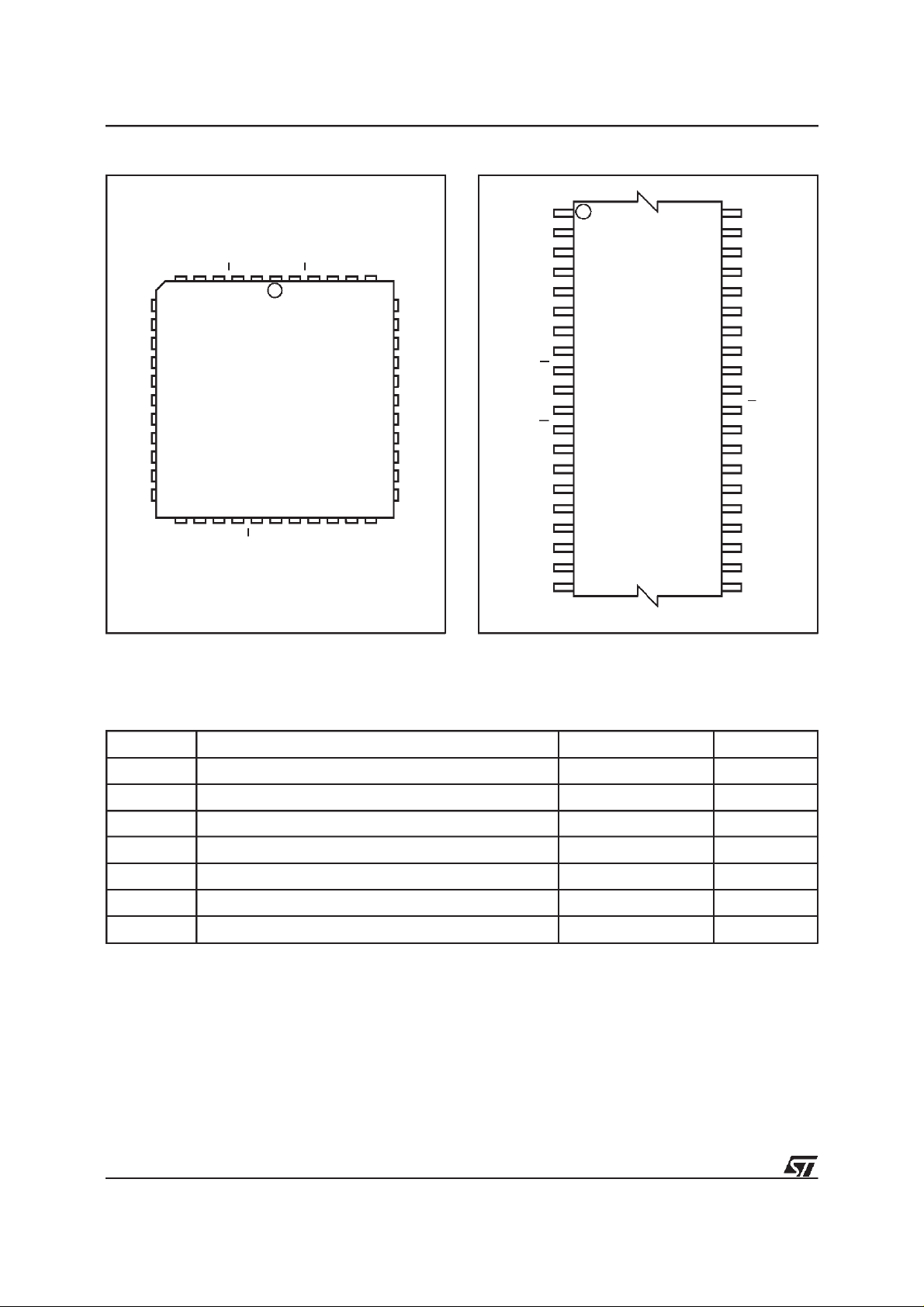
M27C516
Figure2A. LCC Pin Connections
Q13
Q14
Q15
CC
NC
VPPE
V
1
44
Q12
Q11
Q10
Q9 A10
Q8
V
SS
12
M27C516
NC
Q6
Q5
Q4
23
G
Q3
Q2
Q1
Q0
NC
A0
P
A1
NC
A2
NC
A3
A14
34
A4
A13
A12
A11
A9
V
SS
NC
A8Q7
A7
A6
A5
AI00934
Figure2B. TSOPPin Connections
A9
A10
A11
A12 A6
A13 A5
A14
NC
NC
V
CC
V
PP
DQ15
DQ14
DQ13
DQ12 DQ4
DQ11 DQ5
DQ10
DQ9
DQ8
1
P
M27C516
10
(Normal)
11
E
20 21
40
31
30
AI01600
V
SS
A8
A7
A4
A3
A2
A1
A0
G
DQ0
DQ1
DQ2
DQ3
DQ6
DQ7
V
SS
Warning: NC = Not Connected.
Table2. AbsoluteMaximum Ratings
(1)
Warning: NC = Not Connected.
Symbol Parameter Value Unit
T
A
T
BIAS
T
STG
(2)
V
IO
V
CC
(2)
V
A9
V
PP
Notes:
1. Except for therating ”Operating Temperature Range”, stresses above those listedin the Table ”AbsoluteMaximum Ratings”
may cause permanent damage to the device. These are stress ratings only and operation of the device at these or any other
conditions above those indicated in the Operatingsections of this specification is not implied.Exposure to Absolute Maximum
Rating conditions for extendedperiods may affectdevice reliability.Refer also to the STMicroelectronicsSURE Program and other
relevant quality documents.
2. Minimum DC voltage on Input or Output is –0.5V with possible undershoot to –2.0V for a period less than 20ns. Maximum DC
voltage on Output is V
3. Depends on range.
Ambient OperatingTemperature
TemperatureUnder Bias –50 to 125 °C
Storage Temperature –65 to 150
Input or Output Voltages (except A9) –2 to 7 V
Supply Voltage –2 to 7 V
A9 Voltage –2 to 13.5 V
Program SupplyVoltage –2 to 14 V
+0.5Vwith possible overshoot to VCC+2V for a period less than20ns.
CC
(3)
–40 to 125
C
°
C
°
2/12
Page 3
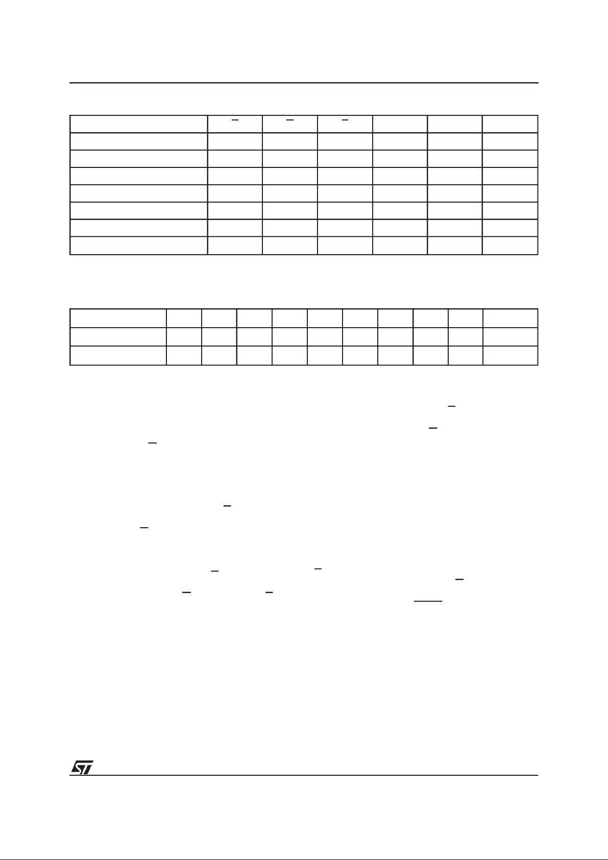
Table3. OperatingModes
M27C516
Mode E G P A9 V
Read V
Output Disable V
Program V
Verify V
Program Inhibit V
Standby V
Electronic Signature V
Notes
or VIL,VID=12V±0.5V
:X=V
IH
IL
IL
IL
IL
IH
IH
IL
V
IL
V
IH
XV
V
IL
XXXVPPHi-Z
XXXVCCHi-Z
V
IL
V
IH
XXVCCHi-Z
Pulse X V
IL
V
IH
V
IH
XVCCData Out
XVPPData Out
V
ID
PP
PP
V
CC
Table4. ElectronicSignature
Identifier A0 Q7 Q6 Q5 Q4 Q3 Q2 Q1 Q0 Hex Data
Manufacturer’s Code V
Device Code V
Note: OutputsQ8-Q15 are set to ’0’.
IL
IH
DEVICEOPERATION
Theoperating modesof theM27C516are listed in
the Operating Modes table.A single power supply
is required in the read mode. All inputs are TTL
levels except for G and 12V on A9 for Electronic
Signature.
ReadMode
The M27C516 has two control functions, both of
which must be logically active in order to obtain
data at the outputs.Chip Enable (E) is the power
control and should be used for device selection.
OutputEnable(G) isthe outputcontrol and should
be used to gate data to the output pins, independent of device selection. Assuming that the
addresses are stable, the address access time
)isequaltothedelayfromE tooutput(t
(t
AVQV
Datais availableatthe outputaftera delayof t
from the falling edge of G, assuming that E has
been low and the addresses have been stablefor
at least t
AVQV-tGLQV
.
StandbyMode
TheM27C516has a standby mode which reduces
00100000 20h
00001111 0Fh
M27C516is placed in the standbymode by applyinga CMOShigh signalto theE input.When in the
standbymode, theoutputsareina highimpedance
state,independentof theG input.
Two Line Output Control
BecauseOTP EPROMsare usually used in larger
memoryarrays,theproductfeaturesa 2linecontrol
functionwhich accommodatesthe use of multiple
memory connection. The two line control function
allows:
a. thelowestpossiblememorypowerdissipation,
b. completeassurance that output bus contention
will not occur.
Forthemostefficientuse ofthesetwo controllines,
ELQV
GLQV
deviceselectingfunction, whileG shouldbe made
a common connection to all devices in the array
E should be decoded and used as the primary
).
and connected to the READ line from the system
controlbus. This ensuresthat all deselectedmemory devices are in their low power standby mode
and that the output pins areonly activewhen data
is requiredfrom a particular memory device.
the supply current from 30mA to 100µA. The
Q0 - Q15
Data In
Codes
3/12
Page 4
M27C516
Table5. AC MeasurementConditions
High Speed Standard
Input Rise and Fall Times ≤ 10ns ≤ 20ns (10% to 90%)
Input Pulse Voltages 0 to 3V 0.4V to 2.4V
Input and Output Timing Ref. Voltages 1.5V 0.8V and 2V
Figure3. ACTestingInput Output Waveform
High Speed
3V
1.5V
0V
Standard
2.4V
0.4V
Table 6. Capacitance
Symbol Parameter Test Condition Min Max Unit
C
IN
C
OUT
Notes. 1. VCCmust be applied simultaneously with or before VPPandremoved simultaneouslywith or after VPP.
2. This parameter is sampled only and not tested 100%.
Input Capacitance VIN=0V 6 pF
Output Capacitance V
=25°C, f =1 MHz)
(T
A
2.0V
0.8V
AI01822
Figure 4. AC TestingLoad Circuit
1.3V
1N914
3.3kΩ
DEVICE
UNDER
TEST
CL= 30pF or 60pF or 100pF
CLincludes JIG capacitance
=0V 12 pF
OUT
OUT
AI02024B
SystemConsiderations
The power switching characteristics of Advanced
CMOS EPROMsrequire careful decouplingof the
devices. The supply current, I
, has three seg-
CC
ments that are of interest to the system designer:
the standby current level, the active current level,
and transientcurrent peaks that are produced by
the falling and risingedges ofE. Themagnitudeof
the transient current peaks is dependent on the
capacitiveandinductiveloadingof thedeviceatthe
output.Theassociatedtransientvoltagepeakscan
be suppressed by complying with the two line
4/12
outputcontroland by properlyselecteddecoupling
capacitors.It is recommendedthat a 1µF ceramic
capacitor be used on every device between V
CC
andVSS. Thisshouldbe a highfrequencycapacitor
of low inherent inductanceand should be placed
as close to the device as possible. In addition, a
4.7µF bulk electrolytic capacitor should be used
betweenV
andVSSforevery eight devices.The
CC
bulk capacitor should be located near the power
supplyconnection point.The purpose of the bulk
capacitor is to overcomethe voltage drop caused
by the inductiveeffectsof PCBtraces.
Page 5

M27C516
Table7. Read Mode DC Characteristics
(1)
(TA=0 to 70 °C or –40 to 85 °C; VCC=5V±5% or 5V± 10%;VPP=VCC)
Symbol Parameter Test Condition Min Max Unit
I
LI
I
LO
I
CC
I
CC1
I
CC2
I
PP
V
V
IH
V
OL
V
OH
Notes: 1. VCCmust be applied simultaneously with or before VPPand removed simultaneously or after VPP.
Input Leakage Current 0V≤V
Output Leakage Current 0V ≤ V
Supply Current E = VIL,G=VIL, f= 5MHz 30 mA
Supply Current (Standby)TTL E = V
Supply Current (Standby) CMOS E > VCC– 0.3V 100
Program Current VPP=V
Input Low Voltage –0.3 0.8 V
IL
(2)
Input High Voltage 2 VCC+1 V
Output Low Voltage IOL= 2.1mA 0.4 V
Output High Voltage TTL IOH= –400µA 2.4 V
Output High Voltage CMOS I
2. Maximum DC Voltage on Output is V
CC
+0.5V.
OH
V
≤
IN
CC
≤ V
OUT
CC
IH
CC
= –100µAV
CC
–0.7V V
1
±
±5 µA
1mA
10 µA
A
µ
A
µ
Table8A. Read Mode AC Characteristics
(1)
(TA=0 to 70 °C or –40 to 85 °C; VCC=5V±5% or 5V± 10%;VPP=VCC)
Symbol Alt Parameter Test Condition
t
AVQVtACC
t
ELQV
t
GLQV
(2)
t
EHQZ
(2)
t
GHQZ
t
AXQX
Notes:
1. V
CC
2. Sampled only, not 100% tested.
3. Speed obtainedwith High Speedmeasurement conditions and a load capacitance of 30pF.
4. Speed obtainedwith a load capacitance of60pF.
Address Validto Output
Valid
Chip Enable Low to
t
CE
Output Valid
Output EnableLow to
t
OE
Output Valid
Chip Enable High to
t
DF
Output Hi-Z
Output EnableHigh to
t
DF
Output Hi-Z
Address Transitionto
t
OH
Output Transition
must be applied simultaneously with or before VPPand removed simultaneously with or after V
E=V
G=V
E=V
G=V
E=V
E=V
,G=V
IL
IL
IL
IL
IL
,G=V
IL
IL
IL
(3)
-35
Min Max Min Max Min Max
35 45 55 ns
35 45 55 ns
18 23 25 ns
018018020ns
018018020ns
000ns
M27C516
(3)
-45
(4)
-55
PP.
Unit
5/12
Page 6

M27C516
Table8B. Read Mode AC Characteristics
(1)
(TA=0 to 70 °C or –40 to 85 °C; VCC=5V±5% or 5V± 10%;VPP=VCC)
M27C516
Symbol Alt Parameter TestCondition
-70
(3)
Min Max Min Max
t
t
AVQV
t
ELQV
t
GLQV
(2)
t
EHQZ
(2)
t
GHQZ
t
AXQX
Notes: 1. VCCmust be applied simultaneously with or before VPPand removed simultaneously with or after V
2. Sampled only, not 100% tested.
3. Speed obtainedwith a load capacitance of60pF
Address Valid to Output Valid E = VIL,G=V
ACC
t
Chip Enable Low to OutputValid G = V
CE
t
Output Enable Low to Output Valid E = V
OE
t
Chip Enable High to Output Hi-Z G = V
DF
t
Output Enable High to Output Hi-Z E = V
DF
Address Transition to
t
OH
Output Transition
E=V
,G=V
IL
IL
IL
IL
IL
IL
0 20 0 30 ns
0 20 0 30 ns
00ns
IL
70 85 ns
70 85 ns
35 35 ns
Figure5. ReadMode AC Waveforms
-85/-10
PP.
Unit
A0-A14
E
G
Q0-Q15
VALID
tAVQV
tGLQV
tELQV
Programming
Whendelivered,all bitsof theM27C516 are inthe
’1’state.Data isintroducedbyselectivelyprogramming ’0’s into the desired bit locations. Although
only’0’s willbe programmed,both ’1’s and’0’s can
bepresentinthedata word.TheM27C516isin the
VALID
tAXQX
tEHQZ
tGHQZ
Hi-Z
AI00935B
programmingmode whenVPPinputis at 12.75V,E
is at V
and P is pulsed to VIL. The data to be
IL
programmedis appliedto 16 bits in parallel to the
data output pins. The evels required for the addressand data inputs are TTL.V
is specifiedto
CC
be 6.25V ±0.25V.
6/12
Page 7

M27C516
Table 9. ProgrammingMode DC Characteristics
(1)
(TA=25°C; VCC= 6.25V± 0.25V;VPP= 12.75V± 0.25V)
Symbol Parameter Test Condition Min Max Unit
I
LI
I
CC
I
PP
V
IL
V
IH
V
OL
V
OH
V
ID
Note: 1. VCCmust be applied simultaneously with or before VPPand removed simultaneously or after VPP.
Table10. ProgrammingMode AC Characteristics
Input Leakage Current VIL≤ VIN≤ V
IH
Supply Current 50 mA
Program Current E = V
IL
Input Low Voltage –0.3 0.8 V
Input High Voltage 2 VCC+ 0.5 V
Output Low Voltage IOL= 2.1mA 0.4 V
Output High Voltage TTL IOH= –400µA 2.4 V
A9 Voltage 11.5 12.5 V
(1)
±10 µA
50 mA
(TA=25°C; VCC=6.25V ± 0.25V;VPP=12.75V ± 0.25V)
Symbol Alt Parameter Test Condition Min Max Unit
t
AVPL
t
QVPL
t
VPHPL
t
VCHPL
t
ELPL
t
PLPH
t
PHQX
t
QXGL
t
t
t
VPS
t
VCS
t
CES
t
PW
t
t
OES
Address Validto Program Low 2
AS
Input Valid to Program Low 2 µs
DS
VPPHigh to Program Low 2
VCCHigh to Program Low 2 µs
Chip Enable Low to
Program Low
2 µs
Program Pulse Width 95 105 µs
Program High to Input
DH
Transition
Input Transitionto Output
Enable Low
2
2 µs
s
µ
s
µ
s
µ
t
GLQV
t
GHQZ
t
GHAX
Notes:
1. V
2. Sampled only and not 100% tested.
t
(2)
t
DFP
t
must be applied simultaneously with or before VPPand removed simultaneously or after VPP.
CC
Output Enable Low to
OE
Output Valid
Output Enable High to
Output Enable High to
AH
Address Transition
Output Hi-Z
100 ns
0 130 ns
0 µs
7/12
Page 8

M27C516
Figure 6. Programmingand Verify Modes AC Waveforms
A0-A14
tAVPL
Q0-Q15
tQVPL
V
PP
tVPHPL
V
CC
tVCHPL
E
tELPL
P
tPLPH
G
Figure 7. ProgrammingFlowchart
VCC= 6.25V, VPP= 12.75V
n=0
P = 100µs Pulse
NO
NO
VERIFY
YES
Last
NO
Addr
YES
CHECK ALL WORDS
1st: VCC=6V
2nd: VCC= 4.2V
++ Addr
YES
++n
=25
FAIL
VALID
DATA IN DATA OUT
tPHQX
tGLQV
tQXGL
PROGRAM VERIFY
PRESTOII ProgrammingAlgorithm
PRESTOII ProgrammingAlgorithm allows to programthe whole array with a guaranteedmargin,in
a typical time of 3 seconds. Programming with
PRESTOII involves the applicationof a sequence
of100µsprogrampulsestoeachbyteuntilacorrect
verify occurs (seeFigure 7). During programming
and verify operation, a MARGIN MODE circuit is
automatically activated in order to guarantee that
each cell is programmedwith enough margin. No
overprogram pulse is applied since the verify in
MARGIN MODE provides necessary margin to
each programmedcell.
ProgramInhibit
Programmingof multipleM27C516sin parallelwith
differentdata is also easilyaccomplished. Except
for E, all like inputs including G of the parallel
M27C516may be common.A TTL low levelpulse
appliedto aM27C516’sP input,withE low andV
at 12.75V,will program that M27C516.Ahigh level
E input inhibits the other M27C516s from being
programmed.
ProgramVerify
AI00707C
A verify (read) should be performed on the programmedbits todeterminethat theywerecorrectly
programmed. The verify is accomplished with E
and G at V
, P at VIH,VPPat 12.75V and VCCat
IL
6.25V.
tGHQZ
tGHAX
AI00936
PP
8/12
Page 9

M27C516
On-BoardProgramming
The M27C516 can be directly programmed in the
application circuit. See the relevant Application
NoteAN620.
ElectronicSignature
The Electronic Signature (ES) mode allows the
reading out of a binarycode froman EPROMthat
will identifyits manufacturerand type. This mode
is intended for use by programmingequipment to
automaticallymatchthe deviceto be programmed
withits correspondingprogrammingalgorithm.The
ES mode is functionalin the 25°C±5°C ambient
temperaturerange that is requiredwhenprogram-
ORDERING INFORMATION SCHEME
Example: M27C516 -70 X N 1 TR
ming the M27C516. Toactivate the ES mode, the
programmingequipmentmustforce11.5Vto 12.5V
on addressline A9 ofthe M27C516.
Two identifier bytes may then be sequencedfrom
thedeviceoutputsby togglingaddressline A0from
V
to VIH. All other addresslines must be held at
IL
during Electronic Signature mode. Byte 0
V
IL
(A0=V
byte 1 (A0=V
) represents the manufacturer code and
IL
) the deviceidentifier code. For the
IH
STMicroelectronicsM27C516, thesetwo identifier
bytes are givenin Table4 andcan be read-outon
outputsQ0 toQ7.
Speed
(1)
-35
-45
-55
-70
-85 85 ns
-10 100 ns
Notes:
35 ns
(1)
45 ns
(2)
55 ns
(2)
70 ns
1. High Speed, see AC Characteristics section for furtherinformation.
2. Speed obtainedwith a load capacitance of60pF.
V
Tolerance
CC
blank ±10%
X ±5%
Package
C PLCC44
N TSOP40
10 x 14mm
Temperature Range
1 0 to 70 °C
6 –40 to 85 °C
Option
TR Tape& Reel
Packing
Fora listof availableoptions (Speed,Package,etc...)orforfurtherinformationon anyaspect ofthis device,
pleasecontact the STMicroelectronicsSales Office nearest to you.
9/12
Page 10

M27C516
PLCC44 - 44 lead PlasticLeaded Chip Carrier, square
Symb
Typ Min Max Typ Min Max
A 4.20 4.70 0.165 0.185
A1 2.29 3.04 0.090 0.120
A2 – 0.51 – 0.020
B 0.33 0.53 0.013 0.021
B1 0.66 0.81 0.026 0.032
D 17.40 17.65 0.685 0.695
D1 16.51 16.66 0.650 0.656
D2 14.99 16.00 0.590 0.630
E 17.40 17.65 0.685 0.695
E1 16.51 16.66 0.650 0.656
E2 14.99 16.00 0.590 0.630
e 1.27 – – 0.050 – –
F 0.00 0.25 0.000 0.010
R 0.89 – – 0.035 – –
N44 44
CP 0.10 0.004
mm inches
D
D1
1N
Ne E1 E
Nd
PLCC
Drawing is not to scale
10/12
R
F
0.51 (.020)
1.14 (.045)
D2/E2
A1
A2
B1
e
B
A
CP
Page 11

TSOP40- 40 lead PlasticThin Small Outline, 10 x 14mm
M27C516
Symb
Typ Min Max Typ Min Max
A 1.20 0.047
A1 0.05 0.15 0.002 0.006
A2 0.95 1.05 0.037 0.041
B 0.17 0.27 0.007 0.011
C 0.10 0.21 0.004 0.008
D 13.80 14.20 0.543 0.559
D1 12.30 12.50 0.484 0.492
E 9.90 10.10 0.390 0.398
e 0.50 – – 0.020 – –
L 0.50 0.70 0.020 0.028
α
N40 40
CP 0.10 0.004
mm inches
0
°
5
°
0
°
5
°
Drawing is not to scale
1N
E
N/2
D1
D
DIE
TSOP-a
A2
e
B
A
CP
C
LA1 α
11/12
Page 12

M27C516
Information furnished is believed to be accurate and reliable. However, STMicroelectronics assumesno responsibility for the consequences
ofuse ofsuch information nor for any infringementof patentsor otherrights of thirdparties whichmay result from its use. No license is granted
by implicationor otherwiseunder any patent or patent rights of STMicroelectronics. Specificationsmentioned in this publicationare subjectto
change without notice. This publication supersedes and replaces all information previously supplied. STMicroelectronics products are not
authorized for use as criticalcomponents in life support devices or systemswithout express written approval of STMicroelectronics.
The ST logo is a registered trademark of STMicroelectronics
1998 STMicroelectronics - AllRights Reserved
Australia - Brazil - Canada - China - France - Germany - Italy - Japan - Korea - Malaysia - Malta- Mexico - Morocco - The Netherlands -
Singapore - Spain - Sweden - Switzerland- Taiwan- Thailand - UnitedKingdom - U.S.A.
STMicroelectronics GROUP OF COMPANIES
12/12
 Loading...