

Page 1
4 Mbit (256Kb x16) UV EPROM and OTP EPROM
5V ± 10% SUPPLYVOLTAGEin READ
OPERATION
FASTACCESSTIME: 45ns
LOW POWERCONSUMPTION:
– ActiveCurrent 70mAat 10MHz
– StandbyCurrent 100µA
PROGRAMMINGVOLTAGE:12.75V ± 0.25V
PROGRAMMINGTIME: 100µs/byte(typical)
ELECTRONICSIGNATURE
– ManufacturerCode: 0020h
– DeviceCode: 0044h
DESCRIPTION
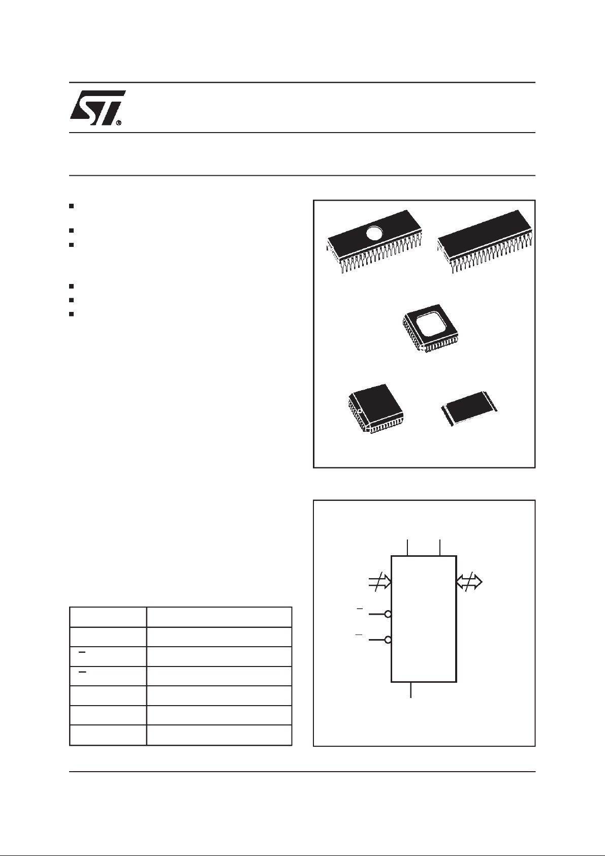
The M27C4002 is a 4 Mbit EPROM offered in the
two ranges UV (ultra violet erase) and OTP (one
time programmable). It is ideally suited for microprocessorsystemsrequiringlargeprogramsandis
organisedas 262,144words of 16 bits.
The FDIP40W(window ceramicfrit-seal package)
and the JLCC44W (J-lead chip carrierpackages)
have transparent lids which allow the user to expose the chip to ultraviolet light to erase the bit
pattern. A new pattern can then be written to the
deviceby followingthe programmingprocedure.
Forapplicationswherethe contentisprogrammed
only one time and erasure is not required, the
M27C4002 is offered in PDIP40, PLCC44 and
TSOP40(10 x 20 mm) packages.
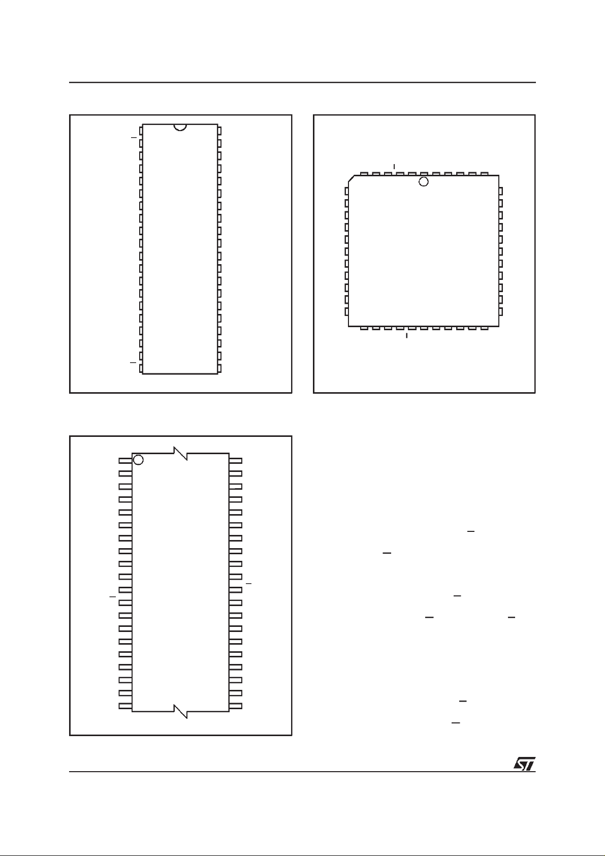
Table1. SignalNames
A0-A17 Address Inputs
M27C4002
40
1
FDIP40W (F)
PLCC44 (C)
Figure1. LogicDiagram
V
18
A0-A17 Q0-Q15
E
40
JLCC44W (J)
V
CC
M27C4002
PP
1
PDIP40 (B)
TSOP40 (N)
10 x 20 mm
16
Q0-Q15 Data Outputs
E Chip Enable
G Output Enable
V
PP
V
CC
V
SS
September 1998 1/16
Program Supply
Supply Voltage
Ground
G
V
SS
AI00727B
Page 2
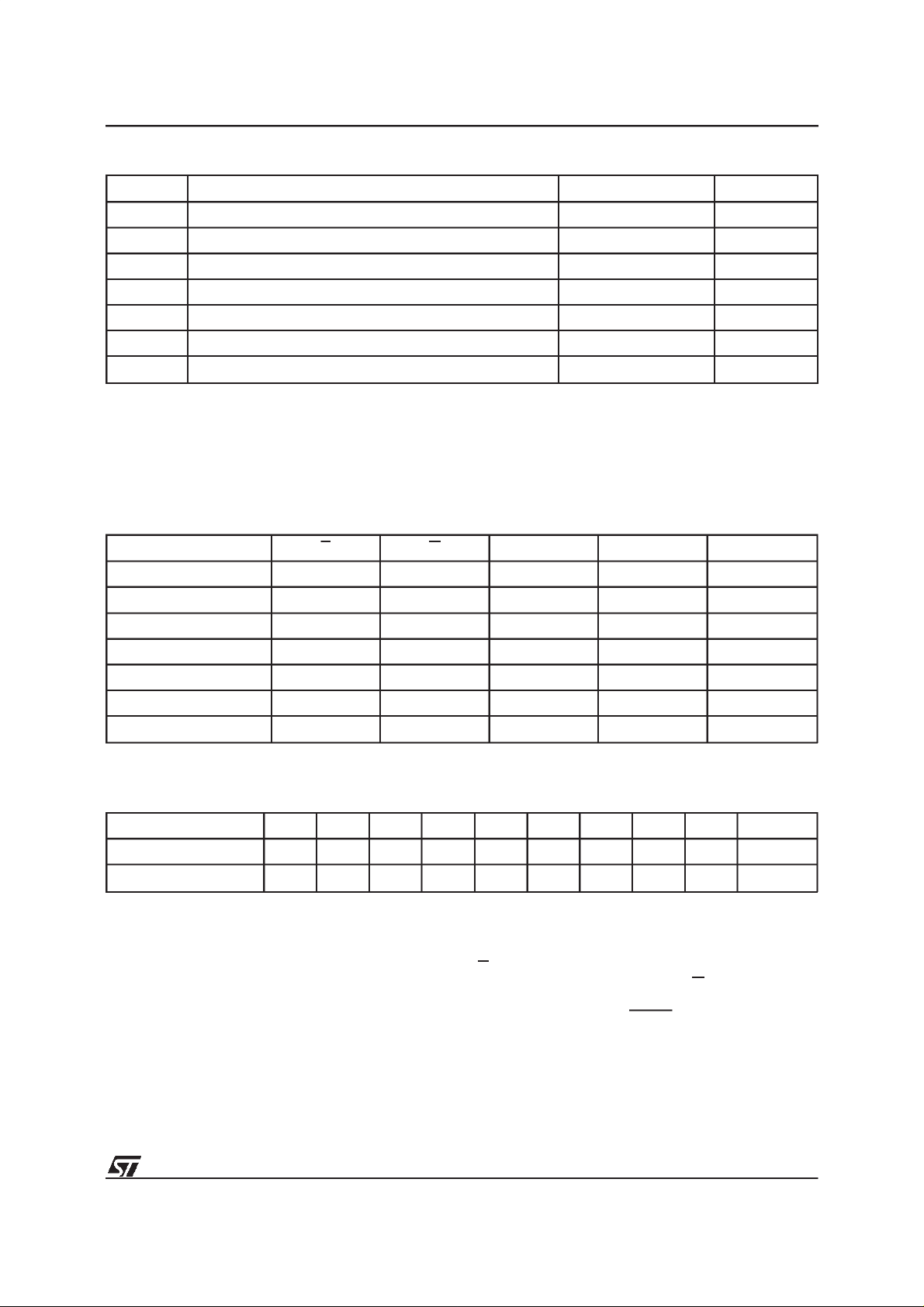
M27C4002
Figure2A. DIP Pin Connections
V
PP
Q15
Q14
Q13
Q12
Q11
Q10
Q9
Q8
V
SS
Q7
Q6
Q5
Q4
Q3
Q2
Q0
1
2
3
4
5
6
7
8
9
10
M27C4002
11
12
13
14
15
16
17
18
19
40
39
38
37
36
35
34
33
32
31
30
29
28
27
26
25
24
23
22
2120
AI00728
V
CC
A17E
A16
A15
A14
A13
A12
A11
A10
A9
V
SS
A8
A7
A6
A5
A4
A3
A2Q1
A1
A0G
Figure2B. LCC Pin Connections
Q15
Q13
Q14
Q12
Q11
Q10
Q9 A10
Q8
V
12
SS
NC
Q6
Q5
Q4
Q3
Warning: NC = Not Connected.
Q2
M27C4002
Q1
Q0
CC
NC
VPPE
V
1
44
23
G
A0
NC
A17
A1
A16
A2
A15
A3
A14
34
A4
A13
A12
A11
A9
V
SS
NC
A8Q7
A7
A6
A5
AI00729
Figure2C. TSOP Pin Connections
A9
A10
A11
A12 A6
A13 A5
A14
A15
A16
A17
V
CC
V
PP
DQ15
DQ14
DQ13
DQ12 DQ4
DQ11 DQ5
DQ10
DQ9
DQ8
1
M27C4002
10
(Normal)
11
E
20 21
40
31
30
AI01831
V
SS
A8
A7
A4
A3
A2
A1
A0
G
DQ0
DQ1
DQ2
DQ3
DQ6
DQ7
V
SS
DEVICEOPERATION
The operating modesof the M27C4002are listed
in the OperatingModes table. A single power supplyis requiredin thereadmode. Allinputs are TTL
levels except for V
and 12V on A9for Electronic
pp
Signature.
Read Mode
The M27C4002 has two control functions,both of
which must be logically active in order to obtain
data at the outputs. Chip Enable (E) is the power
control and should be used for device selection.
OutputEnable(G) is the outputcontrol and should
be used to gate data to the output pins, independent of device selection. Assuming that the
addresses are stable, the address access time
)isequalto thedelayfrom Etooutput(t
(t
AVQV
Datais availableat theoutputaftera delayof t
ELQV
GLQV
from the falling edge of G, assuming that E has
been low andthe addresseshave beenstable for
at least t
AVQV-tGLQV
.
StandbyMode
The M27C4002 has a standby mode which reducesthesupplycurrentfrom50mAto100µA.The
M27C4002 is placed in the standby mode by applyinga CMOShigh signalto theE input. Whenin
thestandbymode,theoutputsare in a highimpedance state,independentof theG input.
).
2/16
Page 3
M27C4002
Table2. Absolute MaximumRatings
(1)
Symbol Parameter Value Unit
T
A
T
BIAS
T
STG
V
IO
V
CC
V
A9
V
PP
Notes: 1. Except for the rating ”Operating Temperature Range”, stresses above those listed in theTable ”AbsoluteMaximum Ratings”
2. Minimum DC voltage on Input or Output is –0.5V with possible undershoot to –2.0V for a period less than 20ns. Maximum DC
3. Depends on range.
Ambient Operating Temperature
Temperature Under Bias –50 to125
Storage Temperature –65 to150
(2)
Input or Output Voltages (except A9) –2 to7 V
Supply Voltage –2 to7 V
(2)
A9 Voltage –2 to13.5 V
Program Supply Voltage –2 to14 V
may cause permanentdamage to thedevice. Theseare stress ratings only and operation of the device at these or any other
conditions above those indicated in the Operatingsections of this specification is not implied.Exposure to Absolute Maximum
Rating conditions for extendedperiods may affectdevice reliability.Refer also to the STMicroelectronicsSURE Programand other
relevant quality documents.
voltage on Output is V
+0.5Vwith possible overshoot to VCC+2V for a period less than20ns.
CC
(3)
–40 to125
C
°
C
°
C
°
Table3. OperatingModes
Mode E G A9 V
Read V
Output Disable V
Program V
Verify V
Program Inhibit V
Standby V
Electronic Signature V
Note:X =VIHor VIL,VID= 12V ± 0.5V
IL
IL
Pulse V
IL
IH
IH
IH
IL
PP
V
IL
V
IH
IH
V
IL
V
IH
XXV
V
IL
XV
XV
CC
CC
or V
or V
SS
SS
XVPPData In
XVPPData Out
XVPPHi-Z
or V
CC
SS
V
ID
V
CC
Q0 - Q15
Data Out
Hi-Z
Hi-Z
Codes
Table4. ElectronicSignature
Identifier A0 Q7 Q6 Q5 Q4 Q3 Q2 Q1 Q0 Hex Data
Manufacturer’s Code V
Device Code V
Note: Outputs Q8-Q15 areset to ’0’.
IL
IH
00100000 20h
01000100 44h
Two Line Output Control
BecauseEPROMsareusuallyusedinlargermemory arrays, the product features a 2 line control
functionwhich accommodatesthe use of multiple
memory connection. The two line control function
allows:
a. the lowest possible memory power dissipation,
b. complete assurancethat output bus contention
will not occur.
Forthemostefficientuse ofthesetwocontrollines,
E should be decoded and used as the primary
deviceselectingfunction,while G shouldbe made
a common connection to all devices in the array
and connected to the READ line from the system
controlbus. This ensuresthat all deselectedmemory devices are in their low power standby mode
and that the output pins areonly active when data
is requiredfrom a particular memory device.
3/16
Page 4
M27C4002
Table5. AC MeasurementConditions
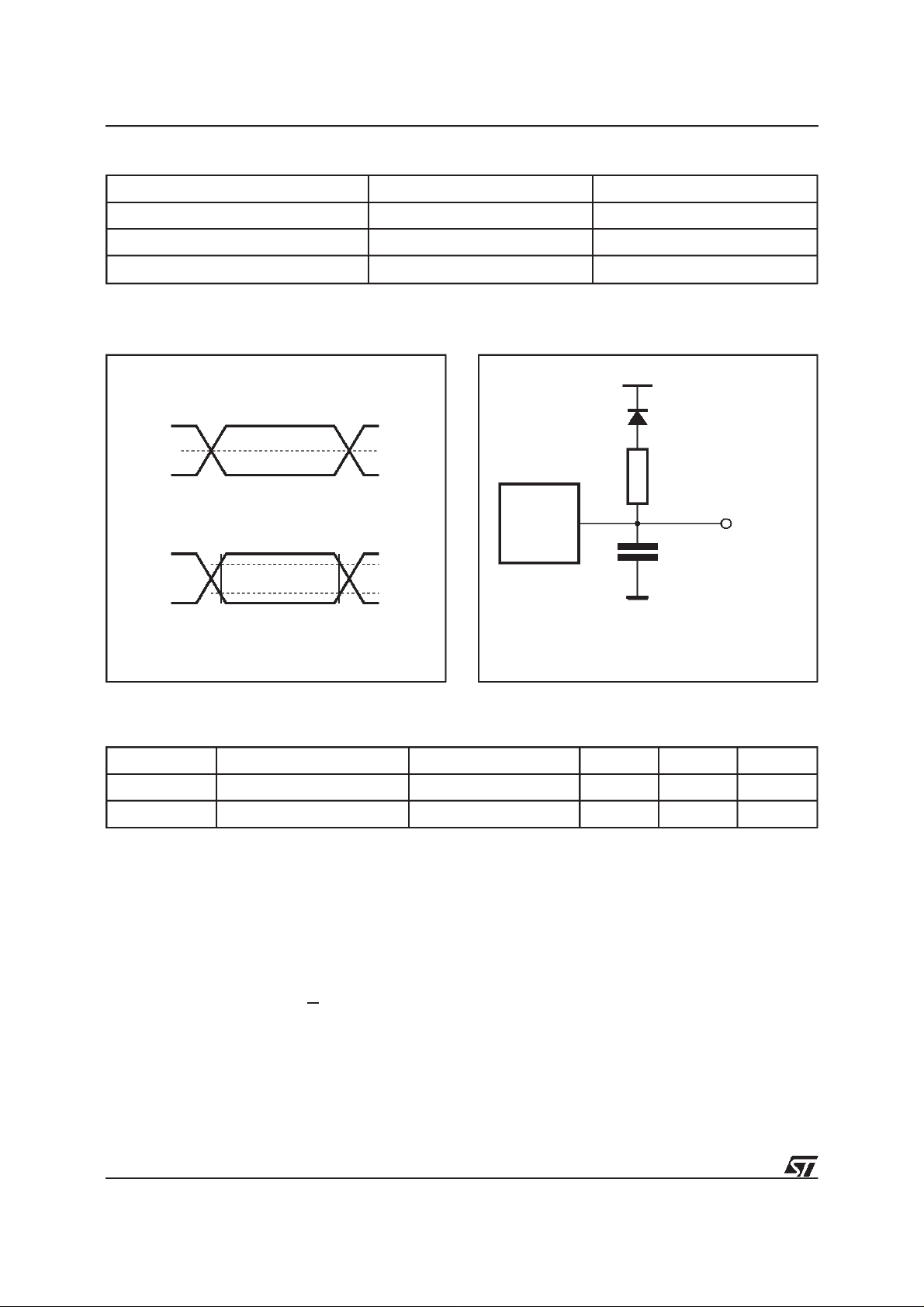
High Speed Standard
Input Rise and Fall Times
Input Pulse Voltages 0 to 3V 0.4Vto 2.4V
Input and Output Timing Ref. Voltages 1.5V 0.8V and 2V
Figure3. ACTestingInput Output Waveform
High Speed
3V
1.5V
0V
Standard
2.4V
0.4V
2.0V
0.8V
AI01822
10ns
≤
Figure4. ACTestingLoad Circuit
1.3V
1N914
3.3kΩ
DEVICE
UNDER
TEST
C
CL= 30pF for High Speed
CL= 100pF for Standard
CLincludes JIG capacitance
L
≤
20ns
OUT
AI01823B
Table6. Capacitance
Symbol Parameter Test Condition Min Max Unit
C
IN
C
OUT
Note: 1. Sampled only,not 100% tested.
SystemConsiderations
The power switching characteristicsof Advanced
CMOS EPROMsrequire careful decoupling of the
devices. The supply current, I
ments that are of interest to the system designer:
the standby currentlevel, the active current level,
and transientcurrent peaks that are produced by
thefalling and rising edgesof E. Themagnitudeof
the transient current peaks is dependent on the
output capacitive and inductiveloading of the device.
(1)
(TA=25°C, f = 1MHz )
Input Capacitance VIN=0V 6 pF
Output Capacitance V
=0V 12 pF
OUT
control and by properly selected decoupling capacitors. Itis recommendedthat a 0.1µF ceramic
capacitor be used on every device between V
, has three seg-
CC
andVSS. Thisshouldbea highfrequencycapacitor
of low inherent inductance and should be placed
as close to the device as possible. In addition, a
4.7µF bulk electrolytic capacitor should be used
betweenV
andVSSfor everyeight devices. The
CC
bulk capacitor should be located near the power
supply connection point.The purpose of the bulk
capacitoris to overcome the voltage drop caused
by the inductive effectsof PCBtraces.
The associated transient voltage peaks can be
suppressed by complying with the two line output
4/16
CC
Page 5
M27C4002
Table7. Read Mode DC Characteristics
(1)
(TA=0 to 70 °C or –40 to 85 °C;VCC=5V±5% or 5V± 10%;VPP=VCC)
Symbol Parameter Test Condition Min Max Unit
I
LI
I
LO
I
CC
I
CC1
I
CC2
I
PP
V
IL
V
IH
V
OL
V
OH
Notes: 1. VCCmust be applied simultaneously with or before VPPand removed simultaneously or after V
2. Maximum DC voltage on Output is VCC+0.5V.
Input Leakage Current 0V ≤ VIN≤ V
Output LeakageCurrent 0V≤V
E=V
= 0mA, f = 10MHz
I
Supply Current
OUT
E=V
I
= 0mA, f = 5MHz
OUT
Supply Current (Standby)TTL E = V
≤
OUT
,G=VIL,
IL
,G=VIL,
IL
IH
CC
V
CC
Supply Current (Standby)CMOS E > VCC–0.2V 100
Program Current VPP=V
CC
Input Low Voltage –0.3 0.8 V
(2)
Input High Voltage 2 VCC+1 V
Output LowVoltage IOL= 2.1mA 0.4 V
Output HighVoltageTTL IOH= –400µA 2.4 V
Output High Voltage CMOS I
= –100µAV
OH
CC
– 0.7V V
PP.
±10 µA
10
±
70 mA
50 mA
1mA
10 µA
A
µ
A
µ
Table8A. Read ModeAC Characteristics
(1)
(TA=0 to 70 °C or –40 to 85 °C;VCC=5V±5% or 5V± 10%;VPP=VCC)
Symbol Alt Parameter
Test
Condition
-45
(3)
Min Max Min Max Min Max Min Max
t
AVQV
t
ELQV
t
GLQV
(2)
t
EHQZ
(2)
t
GHQZ
t
AXQX
Notes: 1. VCCmust be applied simultaneously with or before VPPand removed simultaneously or after V
2. Sampled only, not 100% tested.
3. In case of 70ns speed see High Speed AC Measurement conditions.
Address Valid to
t
ACC
Output Valid
Chip Enable Low
t
CE
to Output Valid
Output Enable
t
OE
Low to Output Valid
Chip Enable High
t
DF
to Output Hi-Z
Output Enable
t
DF
High to Output Hi-Z
Address Transition
t
OH
to Output Transition
E=VIL,
G=V
G=V
E=V
G=V
E=V
E=VIL,
G=V
IL
IL
IL
IL
IL
IL
45 60 80 90 ns
45 60 80 90 ns
25 30 40 40 ns
0 30 0 30 0 30 0 30 ns
0 30 0 30 0 30 0 30 ns
0000ns
-60
(3)
M27C4002
-80 -90
PP.
Unit
5/16
Page 6

M27C4002
Table8B. ReadMode AC Characteristics
(1)
(TA=0 to 70 °C or –40 to 85 °C;VCC=5V±5% or 5V± 10%;VPP=VCC)
M27C4002
Symbol Alt Parameter
t
AVQVtACC
t
ELQV
Address Valid to
Output Valid
Chip Enable Low
t
CE
to Output Valid
Output Enable
t
t
EHQZ
t
GHQZ
GLQV
(2)
(2)
Low to Output
t
OE
Valid
Chip Enable High
t
DF
to Output Hi-Z
Output Enable
High to Output
t
DF
Hi-Z
Address
t
AXQX
t
Transitionto
OH
Output Transition
Test
Condition
E=VIL,
G=V
IL
G=V
IL
E=V
IL
G=V
IL
E=V
IL
E=V
,
IL
G=V
IL
-10 -12 -15 -20
Min Max Min Max Min Max Min Max
100 120 150 200 ns
100 120 150 200 ns
50 60 60 70 ns
0 30 0 40 0 50 0 80 ns
0 30 0 40 0 50 0 80 ns
0000ns
Unit
Figure5. ReadMode AC Waveforms
A0-A17
E
G
Q0-Q15
VALID
tAVQV
tGLQV
tELQV
Programming
When delivered (and after each erasure for UV
EPROM), all bits of the M27C4002 are in the ’1’
state. Data is introduced by selectively programming ’0’s into the desired bit locations. Although
only’0’s willbe programmed,both ’1’s and’0’s can
be present in the data word. The only way to
VALID
tAXQX
tEHQZ
tGHQZ
Hi-Z
AI00731B
changea ’0’to a ’1’is by die exposureto ultraviolet
light (UV EPROM). The M27C4002 is in the programmingmode when V
at V
and E is pulsed to VIL. The data to be
IH
input is at 12.75V,G is
PP
programmedis appliedto 16 bits in parallel to the
data output pins. The levels required for the addressand datainputs are TTL.V
is specifiedto
CC
be 6.25V ± 0.25V.
6/16
Page 7

M27C4002
Table9. ProgrammingMode DCCharacteristics
(1)
(TA=25°C; VCC=6.25V ± 0.25V;VPP=12.75V ± 0.25V)
Symbol Parameter Test Condition Min Max Unit
I
LI
I
CC
I
PP
V
IL
V
IH
V
OL
V
OH
V
ID
Note: 1. VCCmust be applied simultaneously with or before VPPand removed simultaneously or after VPP.
Input Leakage Current 0≤V
Supply Current 50 mA
Program Current E = V
Input Low Voltage –0.3 0.8 V
Input High Voltage 2 VCC+ 0.5 V
Output LowVoltage IOL= 2.1mA 0.4 V
Output HighVoltageTTL IOH= –400µA 2.4 V
A9 Voltage 11.5 12.5 V
Table10. ProgrammingMode AC Characteristics
(1)
V
≤
IN
CC
IL
10
±
50 mA
(TA=25°C; VCC=6.25V ± 0.25V;VPP=12.75V ± 0.25V)
Symbol Alt Parameter Test Condition Min Max Unit
t
AVEL
t
AS
Address Validto Chip Enable Low 2
A
µ
s
µ
t
t
t
t
t
t
t
t
t
DS
VPS
VCS
PW
DH
OES
OE
DFP
AH
t
QVEL
t
VPHEL
t
VCHEL
t
ELEH
t
EHQX
t
QXGL
t
GLQV
t
GHQZ
t
GHAX
Notes: 1. VCCmust be applied simultaneously with or before VPPand removed simultaneously or after VPP.
2. Sampled only, not 100% tested.
Input Valid to Chip Enable Low 2
VPPHigh to Chip EnableLow 2
VCCHighto Chip Enable Low 2
Chip Enable Program Pulse
Width
Chip Enable High to Input
Transition
Input Transition to Output Enable
Low
Output EnableLow to Output
Valid
Output EnableHigh to Output
Hi-Z
Output EnableHigh to Address
Transition
s
µ
s
µ
s
µ
95 105
2
2
s
µ
s
µ
s
µ
100 ns
0 130 ns
0ns
7/16
Page 8

M27C4002
Figure6. Programmingand VerifyModes AC Waveforms
A0-A17
tAVEL
Q0-Q15
V
PP
V
CC
E
G
DATA IN
tQVEL
tVPHEL
tVCHEL
tELEH
Figure7. ProgrammingFlowchart
VCC= 6.25V, VPP= 12.75V
n=0
E = 100µs Pulse
NO
NO
VERIFY
YES
Last
NO
Addr
YES
CHECK ALL WORDS
1st: VCC=6V
2nd: VCC= 4.2V
++ Addr
YES
++n
=25
FAIL
VALID
DATA OUT
tEHQX
tGLQV
tQXGL
PROGRAM VERIFY
PRESTOII ProgrammingAlgorithm
PRESTO II Programming Algorithm allows the
whole array to be programmed with a guaranteed
margin,in a typicaltimeof 26.5seconds.Programming with PRESTO II consists of applying a sequenceof100µs programpulsesto eachbyte until
a correct verify occurs(see Figure 7). Duringprogrammingand verify operation,a MARGINMODE
circuitis automaticallyactivatedin orderto guarantee that each cell is programmed with enough
margin. Nooverprogrampulse isappliedsincethe
verifyin MARGIN MODEprovidesnecessarymargin to each programmedcell.
ProgramInhibit
Programming of multiple M27C4002s in parallel
with different data is also easily accomplished.
Except for E, all like inputs including G of the
parallel M27C4002 may be common. A TTL low
level pulse appliedto a M27C4002’sE input,with
at12.75V,willprogramthatM27C4002. Ahigh
V
PP
level E input inhibits the other M27C4002s from
beingprogrammed.
ProgramVerify
AI00726C
A verify (read) should be performed on the programmedbitsto determinethattheywere correctly
programmed. Theverifyis accomplishedwithG at
, Eat V
V
IL
IH,VPP
tGHQZ
tGHAX
AI00730
at 12.75V and VCCat 6.25V.
8/16
Page 9

M27C4002
On-BoardProgramming
TheM27C4002can be directlyprogrammedin the
application circuit. See the relevant Application
NoteAN620.
ElectronicSignature
The Electronic Signature (ES) mode allows the
reading out of a binarycode froman EPROMthat
will identifyits manufacturer and type. This mode
is intended for use by programmingequipment to
automaticallymatchthe deviceto be programmed
withits correspondingprogrammingalgorithm.The
ES mode is functionalin the 25°C ± 5°C ambient
temperaturerange thatis required whenprogrammingthe M27C4002. ToactivatetheESmode, the
programmingequipmentmustforce 11.5Vto 12.5V
on addres s line A9 of the M27C4002 with
V
PP=VCC
=5V. Two identifier bytes may then be
sequenced from the device outputs by toggling
address line A0 fromV
lines must be held at V
ture mode. Byte 0 (A0=V
facturer code and byte 1 (A0=V
to VIH. All other address
IL
during Electronic Signa-
IL
) represents the manu-
IL
) the device
IH
identifier code. For the STMicroelectronics
M27C4002,these twoidentifier bytes are given in
Table4 andcan be read-outon outputsQ0 toQ7.
ERASUREOPERATION(applies to UV EPROM)
The erasure characteristics of the M27C4002 are
such that erasure begins when the cells are exposed to light with wavelengths shorter than approximately 4000 Å. It should be noted that
sunlightand sometype of fluorescentlamps have
wavelengthsin the3000-4000Å range. Research
shows that constant exposure to room level fluorescentlightingcould erasea typicalM27C4002in
about3 years,while it wouldtake approximately1
week to cause erasure when exposed to direct
sunlight. If the M27C4002 is to be exposed to
thesetypes oflighting conditions for extended periods oftime, it issuggestedthat opaquelabels be
putover theM27C4002windowtopreventunintentional erasure. The recommendederasure procedure for the M27C4002is exposureto shortwave
ultravioletlightwhichhas wavelength2537Å. The
integrateddose (i.e. UV intensityx exposuretime)
forerasureshouldbeaminimumof 15W-sec/cm2.
Theerasuretimewiththis dosage isapproximately
15 to 20 minutes using an ultraviolet lamp with
12000 µW/cm
2
power rating. The M27C4002
shouldbe placed within 2.5cm(1 inch)of thelamp
tubesduring theerasure. Somelampshavea filter
on their tubes which should be removed before
erasure.
9/16
Page 10

M27C4002
ORDERING INFORMATION SCHEME
Example: M27C4002 -70 X C 1 X
Speed
(1)
-45
-60
-80 80 ns
-90 90 ns
-10 100 ns
-12 120 ns
-15 150 ns
-20 200 ns
Note: 1. High Speed, see AC Characteristics section for furtherinformation.
(1)
45 ns
60 ns
V
X
blank
Tolerance
CC
±
±
5%
10%
Package
F FDIP40W
B PDIP40
J JLCC44W
C PLCC44
N TSOP40
10 x 20mm
Temperature Range
1 0 to 70°C
6 –40 to 85°C
Option
X Additional
Burn-in
TR Tape& Reel
Packing
Fora listof available options (Speed,Packageetc...)orfor furtherinformationon anyaspect ofthisdevice,
pleasecontact the STMicroelectronicsSales Office nearestto you.
10/16
Page 11

FDIP40W - 40 pin Ceramic Frit-seal DIP, with window
M27C4002
Symb
A 5.72 0.225
A1 0.51 1.40 0.020 0.055
A2 3.91 4.57 0.154 0.180
A3 3.89 4.50 0.153 0.177
B 0.41 0.56 0.016 0.022
B1 1.45 – – 0.057 – –
C 0.23 0.30 0.009 0.012
D 51.79 52.60 2.039 2.071
D2 48.26 – – 1.900 – –
E 15.24 – – 0.600 – –
E1 13.06 13.36 0.514 0.526
e 2.54 – – 0.100 – –
eA 14.99 – – 0.590 – –
eB 16.18 18.03 0.637 0.710
L 3.18 0.125
S 1.52 2.49 0.060 0.098
∅
α
N40 40
Typ Min Max Typ Min Max
7.62 – – 0.300 – –
mm inches
4
°
11
°
4
°
11
°
Drawing is not to scale.
A2
B1 B e
D2
D
S
N
1
A3A1A
L
α
C
eA
eB
∅
E1 E
FDIPW-a
11/16
Page 12

M27C4002
PDIP40 - 40 pin Plastic DIP, 600 mils width
Symb
Typ Min Max Typ Min Max
A 4.45 – – 0.175 – –
A1 0.64 0.38 – 0.025 0.015 –
A2 3.56 3.91 0.140 0.154
B 0.38 0.53 0.015 0.021
B1 1.14 1.78 0.045 0.070
C 0.20 0.31 0.008 0.012
D 51.78 52.58 2.039 2.070
D2 48.26 – – 1.900 – –
E 14.80 16.26 0.583 0.640
E1 13.46 13.99 0.530 0.551
e1 2.54 – – 0.100 – –
eA 15.24 – – 0.600 –
eB 15.24 17.78 0.600 0.700
L 3.05 3.81 0.120 0.150
S 1.52 2.29 0.060 0.090
α 0° 15° 0É 15É
N40 40
mm inches
Drawing is not to scale.
12/16
B1 B e1
D2
D
S
N
1
A2A1A
E1 E
L
α
C
eA
eB
PDIP
Page 13

M27C4002
JLCC44W - 44 lead Ceramic Chip Carrier J-lead, square window
Symb
Typ Min Max Typ Min Max
A 3.94 4.83 0.155 0.190
A1 2.29 3.05 0.090 0.120
B 0.43 0.53 0.017 0.021
B1 0.66 0.81 0.026 0.032
D 17.40 17.65 0.685 0.695
D1 16.00 16.89 0.630 0.665
D2 14.74 16.26 0.580 0.640
D3 12.70 – – 0.500 – –
E 17.40 17.65 0.685 0.695
E1 16.00 16.89 0.630 0.665
E2 14.74 16.26 0.580 0.640
E3 12.70 – – 0.500 – –
e 1.27 – – 0.050 – –
K 10.16 – – 0.400 – –
N44 44
CP 0.10 0.004
mm inches
E3
Drawing is not to scale.
JLCCW-a
D
D1
1N
K
A1
B1
K
E1 E
D2/E2
e
B
AD3
CP
13/16
Page 14

M27C4002
PLCC44 - 44 lead PlasticLeaded Chip Carrier, square
Symb
Typ Min Max Typ Min Max
A 4.20 4.70 0.165 0.185
A1 2.29 3.04 0.090 0.120
A2 – 0.51 – 0.020
B 0.33 0.53 0.013 0.021
B1 0.66 0.81 0.026 0.032
D 17.40 17.65 0.685 0.695
D1 16.51 16.66 0.650 0.656
D2 14.99 16.00 0.590 0.630
E 17.40 17.65 0.685 0.695
E1 16.51 16.66 0.650 0.656
E2 14.99 16.00 0.590 0.630
e 1.27 – – 0.050 – –
F 0.00 0.25 0.000 0.010
R 0.89 – – 0.035 – –
N44 44
CP 0.10 0.004
mm inches
D
D1
1N
Ne E1 E
Nd
PLCC
Drawing is not to scale.
14/16
R
F
0.51 (.020)
1.14 (.045)
D2/E2
A1
A2
B1
e
B
A
CP
Page 15

TSOP40- 40 lead Plastic Thin Small Outline, 10x 20mm
M27C4002
Symb
Typ Min Max Typ Min Max
A 1.20 0.047
A1 0.05 0.15 0.002 0.006
A2 0.95 1.05 0.037 0.041
B 0.17 0.27 0.007 0.011
C 0.10 0.21 0.004 0.008
D 19.80 20.20 0.780 0.795
D1 18.30 18.50 0.720 0.728
E 9.90 10.10 0.390 0.398
e 0.50 – – 0.020 – –
L 0.50 0.70 0.020 0.028
α
N40 40
CP 0.10 0.004
mm inches
0
°
5
°
0
°
5
°
Drawing is not to scale.
1N
E
N/2
D1
D
DIE
TSOP-a
A2
e
B
A
CP
C
LA1 α
15/16
Page 16

M27C4002
Information furnished is believed to be accurate and reliable. However, STMicroelectronics assumesno responsibility for the consequences
ofuse ofsuch information nor for anyinfringementof patents or other rights of thirdparties which may result from its use. No license is granted
by implicationor otherwiseunder any patent or patent rights of STMicroelectronics. Specificationsmentioned in this publicationare subject to
change without notice. This publication supersedes and replaces all information previously supplied. STMicroelectronics products are not
authorized for use as criticalcomponents in life support devices or systems without express written approval of STMicroelectronics.
The ST logo is a registered trademark of STMicroelectronics
1998 STMicroelectronics - AllRights Reserved
Australia - Brazil - Canada - China - France - Germany - Italy - Japan - Korea - Malaysia - Malta - Mexico - Morocco - The Netherlands -
Singapore - Spain - Sweden - Switzerland - Taiwan- Thailand - UnitedKingdom - U.S.A.
STMicroelectronics GROUP OF COMPANIES
16/16
 Loading...