

Page 1
M27C400
4 Mbit (512Kb x8 or 256Kb x16) UV EPROM and OTP EPROM
■ 5V ± 10% SUPPLY VOLTAGE in READ
OPERATION
■ ACCESS TIME: 55ns
■ BYTE-WIDE or WORD-WIDE
CONFIGURABLE
■ 4 Mbit MASK ROM REPLACEMENT
■ LOW POWER CONSUMPTION
– Active Current 70mA at 8MHz
– Stand-by Current 100µA
■ PROGRAMMI NG VOLT AGE: 12.5V ± 0.25V
■ PROGRAMMING TIME: 100µs/word
■ ELECTRONIC SIGNATURE
– Manufacturer Code: 20h
– Device Code: B8h
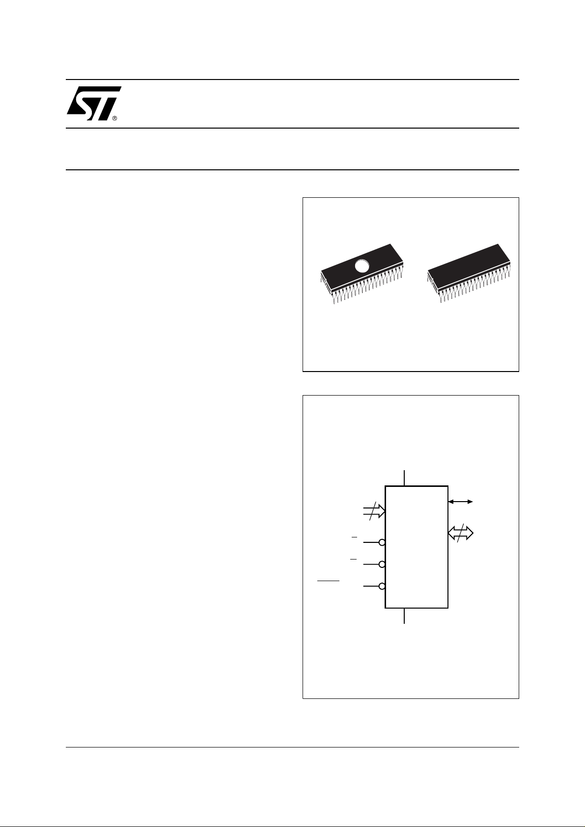
40
1
FDIP40W (F) PDIP40 (B)
Figure 1. Logic Diagram
40
1
DESCRIPTION
The M27C400 is a n 4 Mbit EPROM of fe red i n the
two ranges UV (ultra violet erase) and OTP (one
time programmable). It is ideally suited for microprocessor syst ems requiring large data or program
storage. It is organised as either 512 Kwords of 8
bit or 256 Kwords of 16 bit. The pin-out is compatible with the most common 8 Mbit Mask ROM.
The FDIP40W (window ceramic frit-seal package)
has a transparent lid which all ows the user to expose the chip to ultraviolet light to erase the bit pattern.
A new pattern can then be written rapidly to the device by following the programming procedure.
For applications where the content is programmed
only one time and erasure is not required, the
M27C400 is offered in PDIP40 package.
A0-A17
BYTEV
PP
V
CC
18
E
G
M27C400
V
SS
Q15A–1
15
Q0-Q14
AI01634
1/14May 1999
Page 2
M27C400
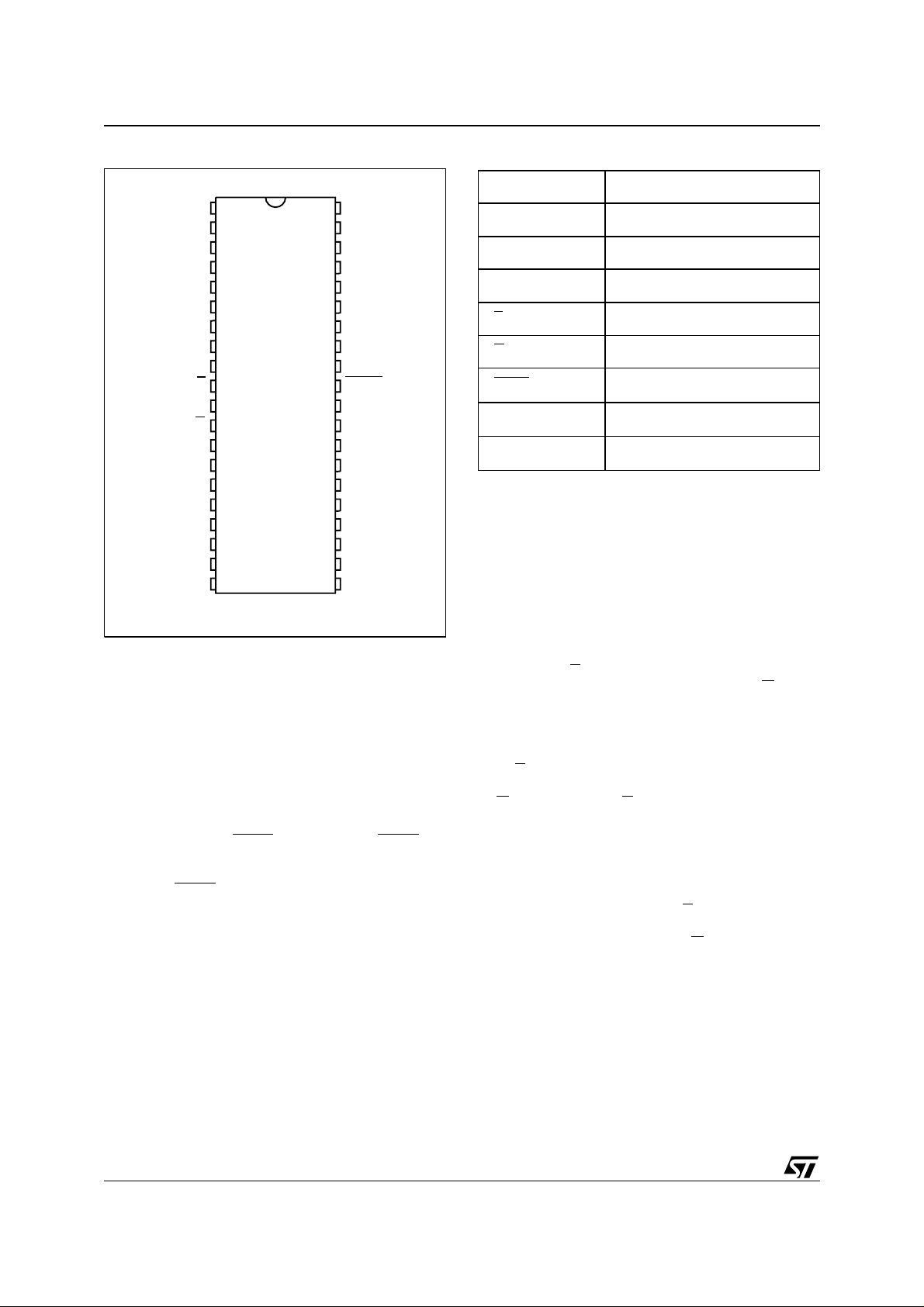
Figure 2. DIP C on ne ctions
A17 A8
A7
A6
A5
A4
A3
A2
A1
A0
V
SS
Q0
Q8
Q1
Q9
Q2
Q3
Q11
1
2
3
4
5
6
7
8
9
E
10
M27C400
11
G
12
13
14
15
16
17
18
19
40
39
38
37
36
35
34
33
32
31
30
29
28
27
26
25
24
23
22
2120
AI01635
A9
A10
A11
A12
A13
A14
A15
A16
BYTEV
V
SS
Q15A–1
Q7
Q14
Q6
Q13
Q5
Q12Q10
Q4
V
CC
PP
DEVICE OPERATION
The operating modes of the M27C400 are listed in
the Operating Modes Table. A single power supply
is required in the read mode. All inputs are TTL
compatib le exce pt for V
and 12V on A9 for the
PP
Electronic Signature.
Read Mode
The M27C400 has two organisations, Word-wide
and Byte-wide. The organisation is selected by the
signal level on the BYTE
VPP pin. When BYTEV
PP
is at VIH the Word-wide organisation is selected
and the Q15A–1 pin is used for Q15 Data Output.
When the BYTE
VPP pin is at VIL the Byte-wide organisation is selected and the Q15A–1 pin is used
for the Address Input A–1. When the memory is
Table 1. Signal Names
A0-A17 Address Inputs
Q0-Q7 Data Outputs
Q8-Q14 Data Outputs
Q15A–1 Data Output / Address Input
E
G
BYTE
V
CC
V
SS
V
PP
Chip Enable
Output Enable
Byte Mode / Program Supply
Supply Voltage
Ground
logically regarded as 16 bit wid e, but read in the
Byte-wide organisation, then with A–1 at V
IL
the
lower 8 bits of the 16 bit data are selected and with
A–1 at V
the upper 8 bits of the 16 bit dat a are
IH
sele cte d.
The M27C400 has two cont rol functions, both of
which must be logically ac tive in order to obtain
data at the outputs. In addition the Word-wide or
Byte- wide organisation must be selected.
Chip Enable (E
used for device selection. Output Enable (G
) is the power control and should be
) is the
output control and should be used to gate data to
the output pins i ndependent of device selection.
Assuming that the addresses are s table, the address access time (t
from E
to output (t
ELQV
output after a delay of t
, assuming that E has been low and the ad-
of G
dresses have been stable for at least t
) is equal to the delay
AVQV
). Data is available at the
from the falling e dge
GLQV
AVQV-tGLQV
Standby Mode
The M27C400 has a standby mode which reduces
the supply current from 50mA to 100µA. The
M27C400 is placed in the standby mode by applying a CMOS high signal to the E
input. When in the
standby mode, the outputs are in a high impedance state, independent of the G
input.
.
2/14
Page 3
M27C400
Table 2. Absolute Maximum Ratings
(1)
Symbol Parameter Value Unit
T
A
T
BIAS
T
STG
(2)
V
IO
V
CC
(2)
V
A9
V
PP
Note: 1. Except for the rating “Oper at i ng Temperature Ra nge”, stresses above those li sted in t he Table “A bsolute Maximum Ratings” m ay
cause permanent damage to the device. These are stress ratings only and operation of the device at these or any other conditions
above those indi cated in t he Operating sect i ons of thi s specif i cation is not imp l i ed. Exposu re to Absolute Ma xim um Rati ng condi tions for extended per iods may aff ect device reliabilit y. Refer also to the STMicroel ectronics SURE Program an d other relevan t qual ity docum en ts .
2. Minimum DC vo ltage on Inpu t or Out put is – 0.5V w ith po ssible un dersh oot to –2.0V fo r a pe riod les s than 20ns. Ma ximu m DC
voltage on Output is V
3. Depends on range.
Ambient Operating Temperature
Temperature Under Bias –50 to 125 °C
Storage Temperature –65 to 150 °C
Input or Output Voltage (except A9) –2 to 7 V
Supply Voltage –2 to 7 V
A9 Voltage –2 to 13.5 V
Program Supply Voltage –2 to 14 V
+0.5V with possible overshoot to VCC +2V for a period l ess than 20ns.
CC
(3)
–40 to 125 °C
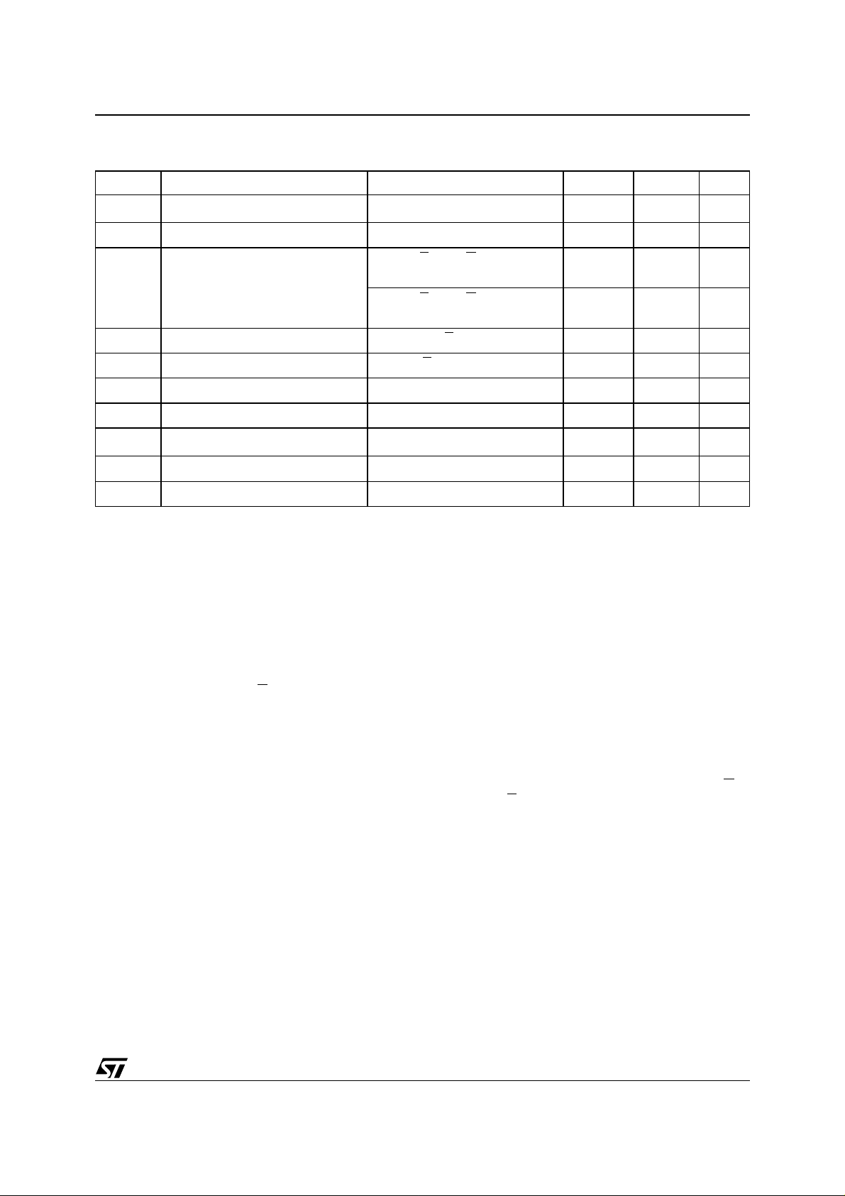
Table 3. Operating Modes
Mode E
Read Word-wide
Read Byte-wide Upper
Read Byte-wide Lower
Output Disable
Program
V
IL
Verify
Program Inhibit
Standby
Electronic Signature
Note: X = VIH or VIL, VID = 12V ± 0.5V.
V
IL
V
IL
V
IL
V
IL
Pulse V
V
IH
V
IH
V
IH
V
IL
V
V
V
V
V
V
V
BYTEV
G
IL
IL
IL
IH
IH
IL
IH
V
IH
V
IL
V
IL
X X Hi-Z Hi-Z Hi-Z
V
PP
V
PP
V
PP
A9 Q7-Q0 Q14-Q8 Q15A–1
PP
X Data Out Data Out Data Out
X Data Out Hi-Z
X Data Out Hi-Z
X Data In Data In Data In
X Data Out Data Out Data Out
X Hi-Z Hi-Z Hi-Z
V
IH
V
IL
X X X Hi-Z Hi-Z Hi-Z
IL
V
IH
V
ID
Codes Codes Code
Table 4. Electronic Signature
Identifier A0 Q7 Q6 Q5 Q4 Q3 Q2 Q1 Q0 Hex Data
Manufacturer’s Code
Device Code
Note: O ut puts Q15-Q8 ar e set to '0'.
V
IL
V
IH
00100000 20h
10110010 B2h
3/14
Page 4
M27C400
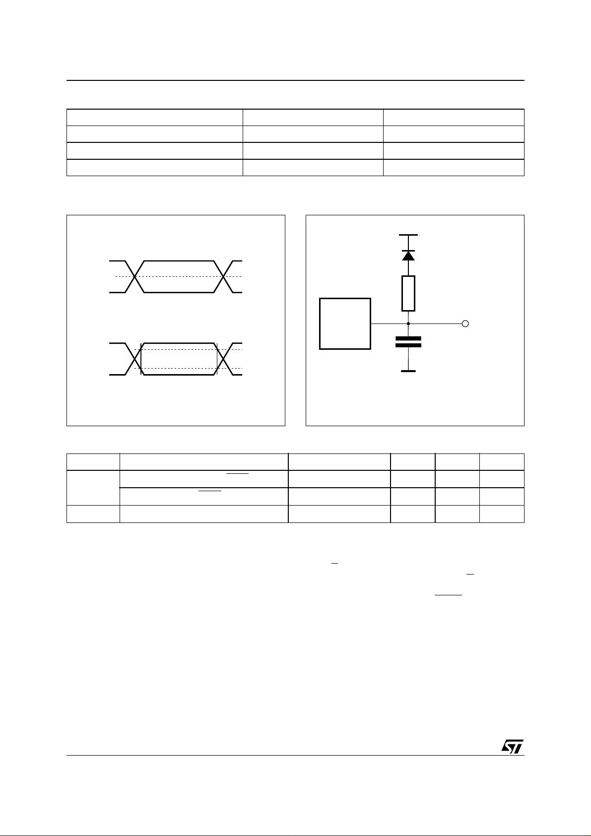
Table 5. AC Measurement Conditions
High Speed Standard
Input Rise and Fall Times
Input Pulse Voltages 0 to 3V 0.4V to 2.4V
Input and Output Timing Ref. Voltages 1.5V 0.8V and 2V
10ns
≤
20ns
≤
Figure 3. Tes ting Inp ut Output Wav ef orm
High Speed
3V
1.5V
0V
Standard
2.4V
0.4V
Table 6. Capacitance
(1)
(TA = 25 °C, f = 1 MHz)
2.0V
0.8V
AI01822
Figure 4. AC Testing Load Circuit
1.3V
1N914
3.3kΩ
DEVICE
UNDER
TEST
CL
CL = 30pF for High Speed
CL = 100pF for Standard
CL includes JIG capacitance
OUT
Symbol Parameter Test Condition Min Max Unit
C
Input Capacitance (except BYTEVPP)V
IN
C
OUT
Note: 1. Sampled only, not 100% tested.
Input Capacitance (BYTE
Output Capacitance
VPP)V
V
IN
IN
OUT
= 0V
= 0V
= 0V
10 pF
120 pF
12 pF
AI01823B
Two Line Outp ut C ontrol
Because EPROMs are usually used in larger
memory arrays, this product features a 2-line control function which accommodates the use of multiple memory connection. The two-line control
function allows:
a. the lowest possible memory power dissipation
b. complete assurance that output bus contention
will not occur.
4/14
For the most efficient use of these two control
lines, E
ry device selecting function, while G
should be decoded and used as the prima-
should be
made a common connectio n to all devices in the
array and connected to the READ
line from the
system control bus. This ensures that all deselected memory devices are in their low power standby
mode and that the output pins are only active
when data is required from a particular memory
device.
Page 5
M27C400
Table 7. Read Mode DC Characteristics
(1)
(TA = 0 to 70 °C or –40 to 85 °C; VCC = 5V ± 5% or 5V ± 10%; VPP = VCC)
Symbol Parameter Test Condition Min Max Unit
I
I
I
CC
I
CC1
I
CC2
I
V
V
IH
V
V
Note: 1. VCC must be ap pl i e d simultaneously with or before VPP and removed simultaneously or af t e r VPP.
Input Leakage Current
LI
Output Leakage Curren t
LO
Supply Current
Supply Current (Standby) TTL
Supply Current (Standby) CMOS
Program Current
PP
Input Low Voltage –0.3 0.8 V
IL
(2)
Input High Voltage 2
Output Low Voltage
OL
Output High Voltage TTL
OH
2. Maximu m DC voltage on Output is V
CC
+0.5 V.
I
I
0V
0V ≤ V
E
OUT
E
OUT
E
≤ V
V
≤
IN
OUT
= VIL, G = VIL,
= 0mA, f = 8MHz
= VIL, G = VIL,
= 0mA, f = 5MHz
E
= V
> VCC – 0.2V
V
= V
PP
I
= 2.1mA
OL
I
= –400µA
OH
≤ V
IH
CC
CC
CC
±1 µA
±10 µA
70 mA
50 mA
1mA
100 µA
10 µA
V
+ 1
CC
0.4 V
2.4 V
V
System Considerations
The power switching characteristics of Advanced
CMOS EPROMs require careful decoupling of the
supplies to the devices. The supply current I
CC
has three segments of importance to the system
designer: the standby current, the active current
and the transient peaks that are produc ed by the
falling and rising edges of E
. The magnitude of the
transient current peaks is dependent on the capacitive and inductive loadi ng of the device outputs. The associated transient voltage peaks can
be suppressed by complying with the two line output control and by properly selected decoupling
capacitors. It is recommended that a 0.1µF ceramic capacitor is used on every device between V
CC
and VSS. This should be a high frequency type of
low inherent inductance and should be placed as
close as possible to the device. In addition, a
4.7µF electrolytic capacitor should be used between V
and VSS for every eight devices. This
CC
capacitor should be mounted near the power supply connection point. The purpose of this capacitor
is to overcome the voltage d r op caus ed by the inductiv e effects of PCB traces.
Programming
When delivered (and after each erasure for UV
EPROM), all bits of the M27C400 are in the '1'
state. Data is introduced by selectively program ming '0's into the desired bit locations. Although
only '0's will be programmed, both '1's and '0's can
be present in the data word. The only way to
change a '0' to a '1' is by die exposition to ultraviolet light (UVEPROM). The M 27C400 is in the programming mode when V
and E is p ulse d to VIL. The data to b e pro-
at V
IH
input is at 12.5V, G is
PP
grammed is applied to 16 bits in parallel to the data
output pins. The levels required for the address
and data inputs are TTL. V
is specified to be
CC
6.25V ± 0.25V.
5/14
Page 6

M27C400
Table 8A. Read Mode AC Characteristics
(1)
(TA = 0 to 70 °C or –40 to 85 °C; VCC = 5V ± 5% or 5V ± 10%; VPP = VCC)
Symbol Alt Parameter Test Condition
t
AVQV
t
BHQV
t
ELQV
t
GLQV
t
BLQZ
t
EHQZ
t
GHQZ
t
AXQX
t
BLQX
Note: 1. VCC must be ap pl i e d simultaneously with or before VPP and removed simultaneously or af t e r V
2. Sampled only, not 100% tested.
3. Speed obtained with High Speed m easurement conditions.
Table 8B. Read Mode AC Characteristics
t
Address Valid to Output Valid
ACC
t
BYTE High to Output Valid
ST
t
Chip Enable Low to Output Valid
CE
t
Output Enable Low to Output Valid
OE
(2)
t
BYTE Low to Output Hi-Z
STD
(2)
t
(2)
Chip Enable High to Output Hi-Z
DF
t
Output Enable High to Output Hi-Z
DF
t
Address Transition to Output Transition
OH
t
BYTE Low to Output Transition
OH
(1)
E
= VIL, G = V
E
= VIL, G = V
G
= V
E
= V
E
= VIL, G = V
G
= V
E
= V
E
= VIL, G = V
E
= VIL, G = V
IL
IL
IL
IL
IL
IL
IL
IL
IL
(TA = 0 to 70 °C or –40 to 85 °C; VCC = 5V ± 5% or 5V ± 10%; VPP = VCC)
Symbol Alt Parameter Test Condition
E
= VIL, G = V
E
= VIL, G = V
G
= V
E
= V
E
= VIL, G = V
G
= V
E
= V
E
= VIL, G = V
E
= VIL, G = V
IL
IL
IL
IL
IL
IL
IL
IL
IL
(2)
(2)
(2)
t
Address Valid to Output Valid
ACC
t
BYTE High to Output Valid
ST
t
Chip Enable Low to Output Valid
CE
t
Output Enable Low to Output Valid
OE
t
BYTE Low to Output Hi-Z
STD
t
Chip Enable High to Output Hi-Z
DF
t
Output Enable High to Output Hi-Z
DF
t
Address Transition to Output Transition
OH
t
BYTE Low to Output Transition
OH
t
AVQV
t
BHQV
t
ELQV
t
GLQV
t
BLQZ
t
EHQZ
t
GHQZ
t
AXQX
t
BLQX
Note: 1. VCC must be ap pl i e d simultaneously with or before VPP and removed simultaneously or af t e r V
2. Sampled only, not 100% tested.
M27C400
-55
(3)
-70
Unit
Min Max Min Max
55 70 ns
55 70 ns
55 70 ns
30 35 ns
30 30 ns
0 30 0 30 ns
0 30 0 30 ns
55ns
55ns
PP
M27C400
Unit-80 -100
Min Max Min Max
80 100 ns
80 100 ns
80 100 ns
40 50 ns
40 50 ns
0 40 0 50 ns
0 40 0 50 ns
55ns
55ns
PP
6/14
Page 7

Figure 5. Word-Wide Read Mode AC Waveforms
M27C400
A0-A17
E
G
Q0-Q15
Note: BYTEVPP = VIH.
VALID
tAVQV
tGLQV
tELQV
Figure 6. Byte-Wide Read Mode AC Waveforms
A–1,A0-A17
VALID
VALID
tAXQX
tEHQZ
tGHQZ
Hi-Z
AI01636
VALID
E
G
Q0-Q7
Note: BYTEVPP = V
tAVQV
tGLQV
tELQV
IL.
tAXQX
tEHQZ
tGHQZ
Hi-Z
AI01637
7/14
Page 8

M27C400
Figure 7. BYTE Transition AC Waveforms
A0-A17
A–1
tAVQV
BYTEV
PP
Q0-Q7
tBLQX
Q8-Q15
tBLQZ
Note: C hi p Enable (E) and Output En able (G) = VIL.
Table 9. Programming Mode DC Characteri stics
VALID
VALID
(1)
Hi-Z
tAXQX
tBHQV
DATA OUT
DATA OUT
AI01638B
(TA = 25 °C; VCC = 6.25V ± 0.25V; VPP = 12.5V ± 0.25V)
Symbol Parameter Test Condition Min Max Unit
I
LI
I
CC
I
PP
V
V
V
OL
V
OH
V
Note: 1. VCC must be ap pl i e d simultaneously with or before VPP and removed simultaneously or af t e r VPP.
Input Leakage Current
Supply Current 50 mA
Program Current
Input Low Voltage –0.3 0.8 V
IL
Input High Voltage 2.4
IH
Output Low Voltage
Output High Voltage TTL
A9 Voltage 11.5 12 .5 V
ID
0 ≤ V
E
= V
I
= 2.1mA
OL
I
= –2.5mA
OH
IN
≤ V
IL
CC
3.5 V
±1
50 mA
V
+ 0.5
CC
0.4 V
A
µ
V
8/14
Page 9

M27C400
Table 10. Programming Mode AC Characteristics
(1)
(TA = 25 °C; VCC = 6.25V ± 0.25V; VPP = 12.5V ± 0.25V)
Symbol Alt Parameter Test Condition Min Max Unit
t
AVEL
t
QVEL
t
VPHAV
t
VCHAV
t
ELEH
t
EHQX
t
QXGL
t
GLQV
(2)
t
GHQZ
t
GHAX
Note: 1. V
2. Sampled only, not 100% tested.
t
Address Valid to Chip Enable Low 2 µs
AS
t
Input Valid to Chip Enable Low 2 µs
DS
t
t
t
t
t
must be ap pl i ed simultaneously wi th or befor e VPP and removed simultaneously or aft er VPP.
CC
VPP High to Address Valid
VPS
VCC High to Address Valid
VCS
Chip Enable Program Pulse Width 45 55 µs
PW
t
Chip Enable High to Input Transition 2 µs
DH
Input Transition to Output Enable Low 2 µs
OES
t
Output Enable Low to Output Valid 120 ns
OE
Output Enable High to Output Hi-Z 0 130 ns
DFP
Output Enable High to Address
t
AH
Transition
2µs
2µs
0ns
Figure 8. Programming and Verify Mod es AC Wavefor ms
A0-A17
Q0-Q15
BYTEV
V
CC
E
G
PP
tVPHAV
tVCHAV
VALID
tAVEL
DATA IN DATA OUT
tQVEL
tELEH
PROGRAM VERIFY
tEHQX
tQXGL
tGLQV
tGHQZ
tGHAX
AI01639
9/14
Page 10

M27C400
Figure 9. Programming Flowchart
VCC = 6.25V, VPP = 12.5V
n = 0
E = 50µs Pulse
NO
NO
VERIFY
YES
NO
Last
Addr
YES
CHECK ALL WORDS
BYTEVPP =V
1st: VCC = 6V
2nd: VCC = 4.2V
IH
++ Addr
AI01044B
YES
++n
= 25
FAIL
PRESTO III P rog ra m mi ng Algorithm
The PRESTO III Programming Algorithm allows
the whole array to be program ed with a guaranteed margin in a typical time of 26 secon ds. Programming with PRESTO I II con sists of a pplying a
sequence of 50µs program pulses to e ach word
until a correct verify occurs (see Figure 9). During
programing and verify operation a MARGIN
MODE circuit is automatically activated to guarantee that each cell is programed with e nough margin. No overpromise pulse is applied since the
verify in MARGIN MODE provides the necessary
margin to each programmed cell.
Program Inhibit
Programming of multiple M27C400s in parallel
with different data is also easily accomplished. Except fo r E
, all like inputs including G of the parallel
M27C400 may be common. A TTL low level pulse
applied to a M27C400's E
will program that M27C400. A high level E
input and VPP at 12.5V,
input inhibits the other M27C400s from being programmed.
Program Verify
A verify (read) should be performed on the programmed bits to determine that they were correctly programmed. The verify is accomplished with E
at VIH and G at VIL, VPP at 12.5V and VCC at
6.25V.
On-B oard Programmi ng
The M27C400 can be directly programmed in the
application circuit. See the relevant Application
Note AN620.
Electronic Signature
The Electronic Signature (ES) mode allows the
reading out of a binary code from an EPROM that
will identify its manufac turer and type. This m ode
is intended for use by program ming equipme nt to
automatically match the device to be programmed
with its corresponding programming algorithm.
The ES mode is functional in the 25°C ± 5°C ambient temperature range that is required when programming the M27C400. To activate the ES
mode, the programming equipment must force
11.5V to 12.5V on address line A9 of the
M27C400, with V
PP=VCC
= 5V. Two identifier
bytes may then be sequenced from the device outputs by toggling address line A0 from V
other address lines must be held at V
to VIH. All
IL
during
IL
Electronic Signature mode.
Byte 0 (A0 = V
code and byte 1 (A0 = V
) represents the manufacturer
IL
) the device identifier
IH
code. For the STMicroelectronics M27C400, these
two identifier bytes are given in Table 4 and can be
read-out on outputs Q7 to Q0.
ERASURE OPERATION (applies to UV EPROM)
The erasure characteristics of the M27C400 is
such that erasure begins when the cells are exposed to light with waveleng ths shorter than approximately 4000 Å. It should be noted that
sunlight and some type of fluorescent lamps have
wavelengths in the 3000-4000 Å range. Research
shows that constant exposure to room level fluorescent lighting could erase a typical M27C400 in
about 3 years, while it would take approximately 1
week to cause erasure when exposed to direct
sunlight. If the M27C400 is to be exposed to these
types of lighting conditions for extended periods of
time, it is suggested that opaque labels be put over
the M27C400 window to prevent unintentional erasure. The recommended erasure procedure for
M27C400 is exposure to short wave ultraviolet
light which has a wav eleng th of 2537 Å. The integrated dose (i.e. UV intensity x exposure time) for
erasure should be a minimum of 30 W-sec/cm
The erasure time with this dosage is approximately 30 to 40 minutes using an ultraviolet lamp with
12000 µW/cm
2
power rating. The M27C400
should be placed within 2.5cm (1 inch) of t he l amp
tubes during the erasure. Some lamps have a filter
on their tubes which should be removed before
erasure.
2
.
10/14
Page 11

Table 11. Ordering Information Scheme
Example: M27C400 -70 X F 1 TR
Device Type
M27
Supply Voltage
C = 5V
Device Function
400 = 4 Mbit (512Kb x8 or 256Kb x16)
Speed
(1)
-55
= 55 ns
-70 = 70 ns
-80 = 80 ns
-100 = 100 ns
V
Tolerance
CC
blank = ± 10%
X = ± 5%
M27C400
Package
F = FDIP40W
B = PDIP40
Temperature Range
1 = 0 to 70 °C
6 = –40 to 85 °C
Options
TR = Tape & Reel Packing
Note: 1. High Speed, see AC Characteris tics secti on f or further information.
For a list of available options (Speed, Pac kage, etc...) or for furthe r information on any aspect of this device, please contact the STMicroelectronics Sales Office nearest to you.
11/14
Page 12

M27C400
Table 12. FDIP40W - 40 lead Ceramic Frit-seal DIP with window, Package Mechanical Data
Symb
A 5.72 0.225
A1 0.51 1.40 0.020 0.055
A2 3.91 4.57 0.154 0.180
A3 3.89 4.50 0.153 0.177
B 0.41 0. 56 0.016 0.022
B1 1.45 – – 0.057 – –
C 0.23 0.30 0.009 0.012
D 51.79 52.60 2.039 2.0 71
D2 48.26 – – 1.900 – –
E 15.24 – – 0.600 – –
E1 13.06 13.36 0.514 0.526
e 2.54 – – 0.100 – –
ea. 14.99 – – 0.590 – –
be 16 .18 18.03 0.637 0.710
L 3.18 – 0.125 –
S 1.52 2. 49 0.060 0.098
∅
α
N40 40
Typ Min Max Typ Min Max
8.13 – – 0.320 – –
mm inches
4° 11° 4° 11°
Figure 10. FDIP40W - 40 lead Ceramic Frit-seal DIP with window, Package Outline
A2
B1 B e
A3
A1AL
α
C
eA
D2
eB
D
S
N
∅
1
Drawing is not to scale.
E1 E
FDIPW-a
12/14
Page 13

M27C400
Table 13. PDIP40 - 40 pin Plastic DIP, 600 mils width, Package Mechanical Data
Symb
Typ Min Max Typ Min Max
A4.45 – – 0.175 – –
A1 0.64 0.38 – 0.025 0.0 15 –
A2 3.56 3.91 0.140 0.154
B 0.38 0. 53 0.015 0.021
B1 1.14 1.78 0.045 0.070
C 0.20 0.31 0.008 0.012
D 51.78 52.58 2.039 2.0 70
D2 48.26 – – 1.900 – –
E 14.80 16.26 0.583 0.640
E1 13.46 13.99 0.530 0.551
e1 2.54 – – 0.1 00 – –
ea. 15.24 – – 0.600 –
be 15 .24 17.78 0.600 0.700
L 3.05 3.81 0.120 0.150
S 1.52 2. 29 0.060 0.090
α
N40 40
mm inches
0° 15° 0° 15°
Figure 11. PDIP40 - 40 lead Plastic DIP, 600 mils width, Package Outline
A2
A1AL
B1 B e1
D2
α
eA
eB
D
S
N
E1 E
1
Drawing is not to scale.
C
PDIP
13/14
Page 14

M27C400
Information furnished is believed to be ac curate and reli able. Howev er, STMicroel ectronics assumes no resp onsibility for the cons equences
of use of such information nor for any infringement of patents or other rights of third parties which may result from its use. No license is granted
by implic ation or otherwise under any patent or patent rights of STMi croelectr onics. Specifications menti oned in thi s publicati on are subject
to change without notice. This publication supersedes and replaces all information previously supplied. STMicroelectronics products are not
authorized for use as cri tical comp onents in life support dev i ces or systems wi thout express written approval of STMicroel ectronics.
The ST log o i s registered trademark of STMicroelectronics
1999 ST Microel ectronics - All Ri ghts Rese rved
All other names are the property of their resp ective owner s.
Australi a - Brazil - Canada - China - F rance - Germ any - Italy - Japan - Korea - M al aysia - Malt a - Mexico - Morocco - The Netherlands -
Singapor e - Spain - Sweden - Switzerl and - Taiwan - Thailand - United Kingdom - U.S. A.
STMicroelect ro n ics GRO UP OF COMPANI ES
http://www.st.com
14/14
 Loading...