

Page 1
32 Mbit (4Mb x8 or 2Mb x16) OTP EPROM
■ 5V ± 10% SUPPLY VOLTAGE in READ
OPERATION
■ FAST ACCESS TIME: 80ns
■ BYTE-WIDE or WORD-WIDE
CONFIGURABLE
■ 32 MbitMASK ROM REPLACEMENT
■ LOW POWER CONSUMPTION
– Active Current70mA at 8MHz
– Stand-by Current 100mA
■ PROGRAMMING VOLTAGE: 12V ± 0.25V
■ PROGRAMMING TIME: 100µs/byte
(typical)(PRESTO III Algorithm)
■ ELECTRONIC SIGNATURE:
– Manufacturer Code0020h
– Device Code: 0032h
M27C320
PRELIMINARY DATA
44
1
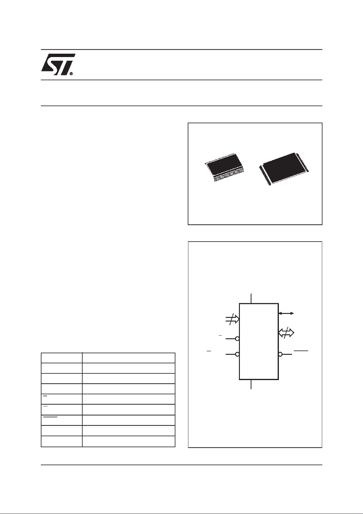
SO44 (M) TSOP48 (N)
12 x20 mm
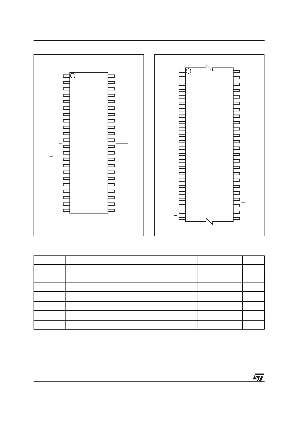
Figure 1. Logic Diagram
DESCRIPTION
The M27C320 is a 32 Mbit EPROM offered in the
OTP range (one time programmable). It is ideally
suited for microprocessor systems requiring large
data or program storage. It is organised as either
4 MWords of 8 bit or 2 MWords of 16 bit. The pinout is compatible with the 32 Mbit Mask ROM.
The M27C320 is offered in TSOP48 (12 x 20mm)
and SO44 packages.
Table 1. Signal Names
A0-A20 Address Inputs
Q0-Q7 Data Outputs
Q8-Q14 Data Outputs
Q15A–1 Data Output / Address Input
E Chip Enable
GV
PP
BYTE Byte-Wide Select
V
CC
V
SS
Output Enable / Program Supply
Supply Voltage
Ground
A0-A20
GV
PP
V
CC
21
Q15A–1
15
Q0-Q14
E
M27C320
BYTE
V
SS
AI02152
September 1998
This is preliminary information on a new product now in development or undergoing evaluation. Details are subject to change without notice.
1/15
Page 2
M27C320
Figure 2A. SO Pin Connections
NC A20
1
2
A7
A6
A5
A4
A3
A2
A1
A0
3
4
5
6
7
8
9
10
11
12
M27C320
E
13
14
15
16
A17 A8
V
SS
GV
PP
Q0
Q8
17Q1
Q9
18
19
Q10
Q3
20
21
Q11
44
43
42
41
40
39
38
37
36
35
34
33
32
31
30
29
28
27
26
25
24
2322
AI02153
A19A18
A9
A10
A11
A12
A13
A14
A15
A16
BYTE
V
SS
Q15A–1
Q7
Q14
Q6
Q13
Q5Q2
Q12
Q4
V
CC
Figure 2B. TSOP Pin Connections
BYTE
A16
A15
A14
A13
A12
A10
A9
A8
A19
V
SS
A20
A18
A17
A7
A6
A5
A4
A2
A1
A0
1
12
M27C320
13
24 25
E
48
37
36
AI02154
V
SS
V
SS
Q15A–1
Q7
Q14
Q6
Q13A11
Q5
Q12
Q4
V
CC
V
CC
V
SS
Q11
Q3
Q10
Q2
Q9
Q1
Q8A3
Q0
GV
PP
V
SS
V
SS
Warning: NC = Not Connected.
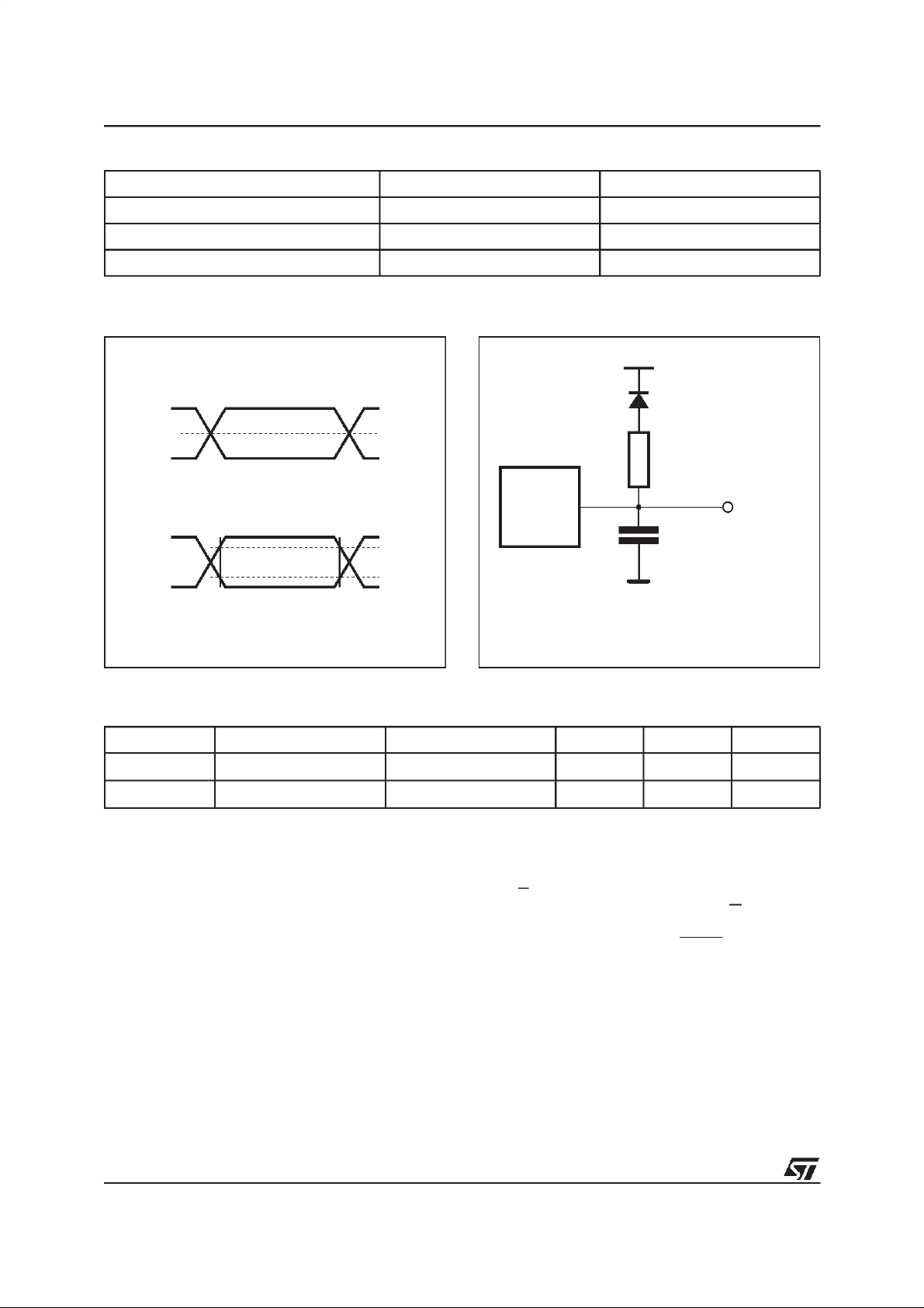
Table 2. Absolute Maximum Ratings
Symbol Parameter Value Unit
T
A
T
BIAS
T
STG
(2)
V
IO
V
CC
(2)
V
A9
V
PP
Note: 1. Except for the rating ”Operating Temperature Range”, stresses above those listedin the Table ”Absolute Maximum Ratings” may
2/15
cause permanent damage to the device. These are stress ratings only and operation of the device atthese or any other conditions
above those indicated in the Operating sections of this specification is not implied. Exposure to Absolute Maximum Rating conditions for extended periodsmay affect device reliability. Referalso to theSTMicroelectronics SUREProgram and other relevant quality documents.
2. Minimum DC voltage on Input or Output is –0.5V with possible undershoot to –2.0V for a period less than 20ns. Maximum DC
voltage on Output is V
3. Depends on range.
Ambient Operating Temperature
Temperature Under Bias –50 to 125 °C
Storage Temperature –65 to 150 °C
Input or Output Voltage (except A9) –2 to 7 V
Supply Voltage –2 to 7 V
A9 Voltage –2 to 13.5 V
Program Supply Voltage –2 to 14 V
+0.5V with possible overshoot to VCC+2V for a period less than 20ns.
CC
(1)
(3)
–40 to 125 °C
Page 3
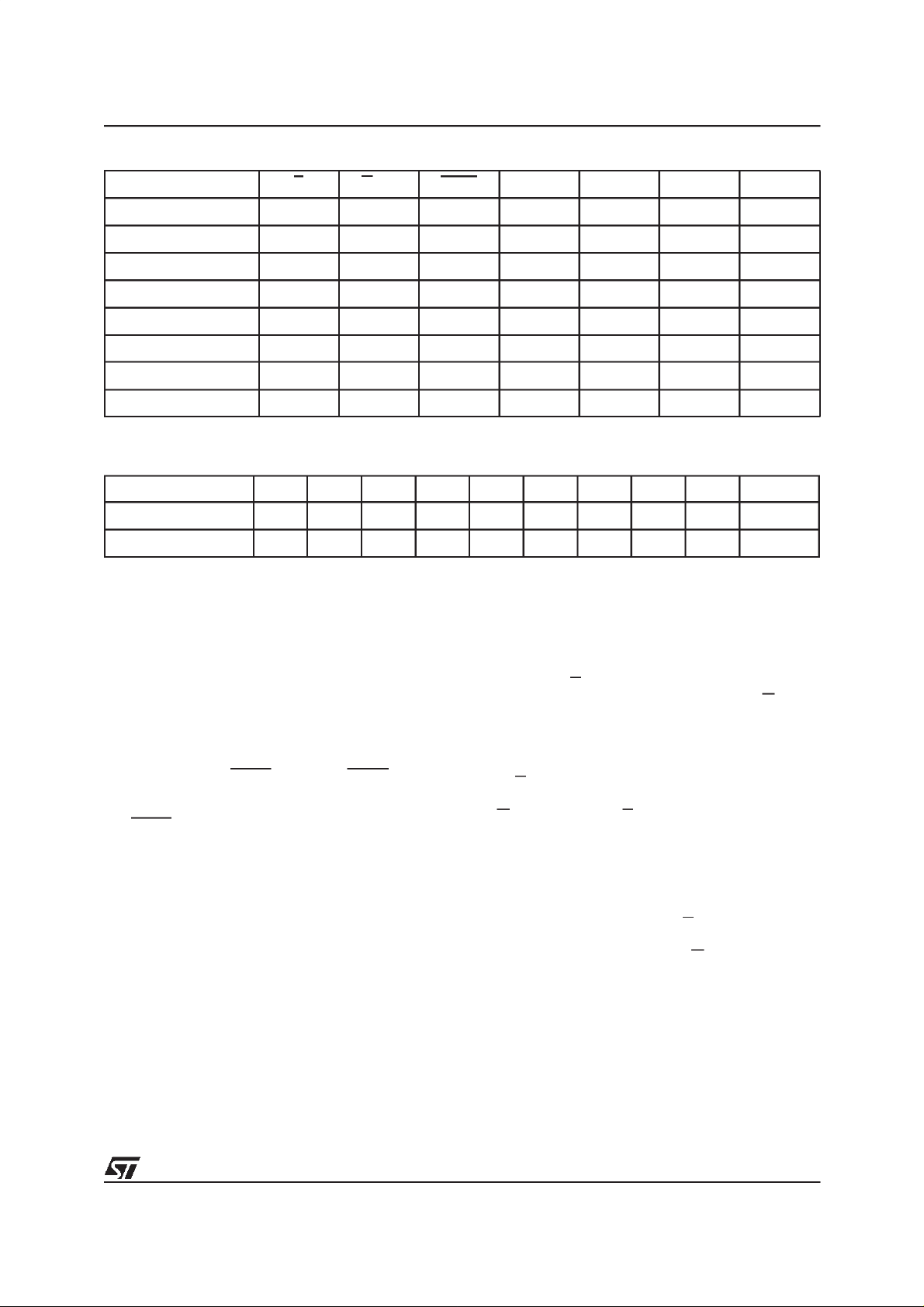
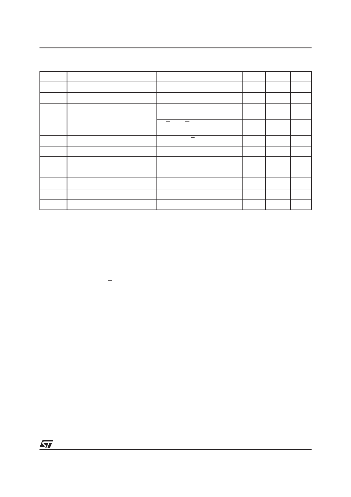
Table 3. Operating Modes
Mode E GV
Read Word-wide
Read Byte-wide Upper V
Read Byte-wide Lower
Output Disable
Program
Program Inhibit
Standby
Electronic Signature
Note: X = VIHor VIL,VID= 12V ± 0.5V.
V
V
V
V
Pulse V
IL
V
IH
V
IH
V
PP
IL
IL
IL
IL
IL
V
IL
V
IL
V
IL
V
IH
PP
V
PP
X X X Hi-Z Hi-Z Hi-Z
V
IL
BYTE A9 Q0-Q7 Q8-Q14 Q15A–1
V
IH
V
IL
V
IL
X X Hi-Z Hi-Z Hi-Z
V
IH
V
IH
V
IH
X Data Out Data Out Data Out
X Data Out Hi-Z V
X Data Out Hi-Z
X Data In Data In Data In
X Hi-Z Hi-Z Hi-Z
V
ID
Codes Codes Code
Table 4. Electronic Signature
Identifier A0 Q7 Q6 Q5 Q4 Q3 Q2 Q1 Q0 Hex Data
Manufacturer’s Code
Device Code V
Note: Outputs Q8-Q15 are set to ’0’.
V
IL
IH
00100000 20h
00110010 32h
M27C320
IH
V
IL
DEVICE OPERATION
The operatingmodes ofthe M27C320 are listed in
the OperatingModes Table.A single power supply
is required in the read mode. All inputs are TTL
compatible except for VPPand 12V on A9 for the
Electronic Signature.
Read Mode
The M27C320 has two organisations, Word-wide
and Byte-wide.The organisationis selected by the
signal level ontheBYTE pin. WhenBYTE is at V
IH
the Word-wide organisation is selected and the
Q15A–1 pin is used for Q15 Data Output. When
the BYTE pin is at VILthe Byte-wide organisation
is selected andthe Q15A–1 pin is used for the Address Input A–1. When the memory is logically regarded as 16 bit wide, but read in the Byte-wide
organisation, then with A–1 at VILthe lower 8 bits
of the 16 bit data are selected and with A–1at V
IH
the upper 8 bits of the 16 bit data are selected.
The M27C320 has two control functions, both of
which must be logically active in order to obtain
data at the outputs. In addition the Word-wide or
Byte-wide organisation must be selected.
Chip Enable (E) is thepower control andshould be
used fordevice selection.Output Enable (G) is the
output control and should be used to gate data to
the output pins independent of device selection.
Assuming that the addresses are stable, the address access time (t
from E to output (t
ELQV
output after a delay of t
) is equal to the delay
AVQV
). Data is available at the
from the falling edge
GLQV
of G, assuming that E has been low and the addresseshave beenstable for atleast t
AVQV-tGLQV
Standby Mode
The M27C320 has standby mode which reduces
the supply current from 50mA to 100µA. The
M27C320 is placedin the standby modeby applying aCMOS high signal to the Einput. Whenin the
standby mode, the outputs are in a high impedance state, independent of the G input.
.
3/15
Page 4
M27C320
Table 5. AC Measurement Conditions
High Speed Standard
Input Rise and Fall Times ≤ 10ns ≤ 20ns
Input Pulse Voltages 0 to 3V 0.4V to 2.4V
Input and Output Timing Ref. Voltages 1.5V 0.8V and 2V
Figure 3. Testing Input Output Waveform
High Speed
3V
1.5V
0V
Standard
2.4V
0.4V
Table 6. Capacitance
(1)
(TA=25°C, f = 1 MHz)
2.0V
0.8V
AI01822
Figure 4. AC Testing Load Circuit
1.3V
1N914
3.3kΩ
DEVICE
UNDER
TEST
C
L
CL= 30pF for High Speed
CL= 100pF for Standard
CLincludes JIG capacitance
Symbol Parameter Test Condition Min Max Unit
V
C
IN
C
OUT
Note: 1. Sampled only,not 100% tested.
Input Capacitance
Output Capacitance V
=0V
IN
=0V 12 pF
OUT
10 pF
OUT
AI01823B
Two Line Output Control
Because EPROMs are usually used in larger
memory arrays, this product features a 2 line control function which accommodates the use of multiple memory connection. The two line control
function allows:
a. the lowest possible memory power dissipation,
b. complete assurance that output bus contention
will not occur.
4/15
For the most efficient use of these two control
lines, Eshould be decoded and used astheprimary device selecting function, while G should be
made a common connection to all devices in the
array and connected to the READ line from the
system control bus. This ensures that all deselected memory devices are in their low power standby
mode and that the output pins are only active
when data is required from a particular memory
device.
Page 5
M27C320
Table 7. Read Mode DC Characteristics
(1)
(TA= 0 to 70 °C; VCC=5V±10%)
Symbol Parameter Test Condition Min Max Unit
I
I
I
CC
I
CC
I
CC
I
V
V
IH
V
V
Note: 1. VCCmust be applied simultaneously with or before VPPand removed simultaneously or after VPP.
Input Leakage Current
LI
Output Leakage Current
LO
Supply Current
1
Supply Current (Standby) TTL
2
Supply Current (Standby) CMOS
Program Current
PP
Input Low Voltage –0.3 0.8 V
IL
(2)
Input High Voltage 2
Output Low Voltage
OL
Output High Voltage TTL
OH
2. Maximum DC voltage on Output is V
CC
+0.5V.
E=V
E=V
0V ≤ V
IL
IL
0V ≤ V
,G=VIL,I
,G=VIL,I
E>VCC– 0.2V
I
IN
OUT
f = 8MHz
f = 5MHz
E=V
V
PP=VCC
I
= 2.1mA
OL
=–400µA
OH
≤ V
≤ V
IH
OUT
OUT
CC
CC
= 0mA,
= 0mA,
2.4 V
±1 µA
±10 µA
70 mA
50 mA
1mA
100 µA
10 µA
V
+1
CC
0.4 V
V
System Considerations
The power switching characteristics of Advanced
CMOS EPROMs require carefull decoupliing of
the suppliesto the devices. The supply current I
CC
has three segments of importance to the system
designer: the standby current, the active current
and the transient peaks that are produced by the
falling and rising edges of E.
The magnitude of the transient current peaks is
dependant on the capacititive and inductive loading of the device outputs. The associatedtransient
voltage peaks can be supressed by complying
with the two line output control and byproperly selected decoupling capacitors. It is recommended
that a 0.1µF ceramic capacitor is used on every
device between VCCand VSS. This should be a
high frequency type of low inherent inductance
and should be placed as close as possible to the
device. In addition, a 4.7µF electrolytic capacitor
should be used between VCCand VSSfor every
eight devices. This capacitor should be mounted
near the power supply connection point. The purpose of this capacitor is to overcome the voltage
drop caused by the inductive effects of PCB traces.
Programming
When delivered, allbits of the M27C320 arein the
’1’ state. Data is introduced by selectively programming ’0’s into the desired bit locations. Although only ’0’s will be programmed, both ’1’s and
’0’s can be present in the data word. The
M27C320 is in the programming mode when V
PP
input is at 12.5V, G is at VIHand Eis pulsedto VIL.
The data to be programmed isapplied to 16 bitsin
parallel to the data outputpins. Thelevels required
for the address and data inputs are TTL. VCCis
specified to be 6.25V ± 0.25V.
5/15
Page 6

M27C320
Table 8. Read Mode AC Characteristics
(1)
(TA= 0 to 70 °C; VCC=5V±10%)
M27C320
Symbol Alt Parameter Test Condition
t
AVQVtACC
t
BHQV
t
ELQV
t
GLQV
(2)
t
BLQZ
(2)
t
EHQZ
(2)
t
GHQZ
t
AXQX
t
BLQX
Note: 1. VCCmust be applied simultaneously with or before VPPand removed simultaneously or after V
2. Sampled only, not 100% tested.
Address Valid to Output
Valid
t
BYTE High to Output Valid
ST
Chip Enable Low to Output
t
CE
Valid
Output Enable Low to
t
OE
Output Valid
t
BYTE Low to Output Hi-Z
STD
Chip Enable High to Output
t
DF
Hi-Z
Output Enable High to
t
DF
Output Hi-Z
Address Transition to
t
OH
Output Transition
BYTE Low to Output
t
OH
Transition
E=V
E=V
G=V
E=V
E=V
G=V
E=V
E=V
E=V
,G=V
IL
,G=V
IL
IL
,G=V
IL
IL
,G=V
IL
,G=V
IL
IL
IL
IL
IL
IL
IL
IL
-80 -100 -120
Min Max Min Max Min Max
80 100 120 ns
80 100 120 ns
80 100 120 ns
40 50 60 ns
40 40 50 ns
0 40 0 40 0 50 ns
0 40 0 40 0 50 ns
555ns
555ns
Unit
PP
Figure 5. Word-Wide Read Mode AC Waveforms
A0-A20
E
GV
Q0-Q15
Note: BYTE = VIH.
PP
VALID
tAVQV
tGLQV
tELQV
VALID
tAXQX
tEHQZ
tGHQZ
Hi-Z
AI02207
6/15
Page 7

Figure 6. Byte-Wide Read Mode AC Waveforms
M27C320
A0-A20
E
GV
Q0-Q7
Note: BYTE = VIH.
PP
VALID
tAVQV
tGLQV
tELQV
Figure 7. BYTE Transition AC Waveforms
A0-A20
VALID
tAXQX
tEHQZ
tGHQZ
Hi-Z
AI02218
VALID
A–1
tAVQV
BYTE
Q0-Q7
tBLQX
Q8-Q15
tBLQZ
Note: Chip Enable (E) and Output Enable (G) = VIL.
VALID
Hi-Z
tAXQX
tBHQV
DATA OUT
DATA OUT
AI02219
7/15
Page 8

M27C320
Table 9. Programming Mode DC Characteristics
(1)
(TA=25°C; VCC= 6.25V ± 0.25V; VPP= 12V ± 0.25V)
Symbol Parameter Test Condition Min Max Unit
I
LI
I
CC
I
PP
V
V
V
OL
V
OH
V
Note: 1. VCCmust be applied simultaneously with or before VPPand removed simultaneously or after VPP.
Input Leakage Current
Supply Current 50 mA
Program Current
Input Low Voltage –0.3 0.8 V
IL
Input High Voltage 2.4 VCC+ 0.5 V
IH
Output Low Voltage
Output High Voltage TTL IOH= –2.5mA 3.5 V
A9 Voltage 11.5 12.5 V
ID
Table 10. MARGINMODE AC Characteristics
(1)
V
IL
I
OL
≤ VIN≤ V
E=V
IL
= 2.1mA
IH
±10 µA
50 mA
0.4 V
(TA=25°C; VCC= 6.25V ± 0.25V; VPP= 12V ± 0.25V)
Symbol Alt Parameter Test Condition Min Max Unit
t
A9HVPH
t
VPHEL
t
A10HEH
t
A10LEH
t
EXA10X
t
EXVPX
t
VPXA9X
Note: 1. VCCmust be applied simultaneously with or before VPPand removed simultaneously or after VPP.
t
t
t
AS10VA10
t
AS10VA10
t
AH10
t
t
VA9High to VPPHigh
AS9
VPSVPP
Chip Enable Transition to V
Chip Enable Transition to VPPTransition 2 µs
VPH
VPPTransition to VA9Transition
AH9
High to Chip Enable Low
High to Chip Enable High (Set)
Low to Chip Enable High (Reset)
Transition
A10
2 µs
2 µs
1 µs
1 µs
1 µs
2 µs
8/15
Page 9

M27C320
Table 11. ProgrammingMode AC Characteristics
(1)
(TA=25°C; VCC= 6.25V ± 0.25V; VPP= 12V ± 0.25V)
Symbol Alt Parameter TestCondition Min Max Unit
t
AVEL
t
QVEL
t
VCHEL
t
VPHEL
t
VPLVPH
t
ELEH
t
EHQX
t
EHVPX
t
VPLEL
t
ELQV
(2)
t
EHQZ
t
EHAX
Note: 1. VCCmust be applied simultaneously with or before VPPand removed simultaneously or after VPP.
2. Sampled only, not 100% tested.
t
t
t
VCS
t
OES
t
PRT
t
PW
t
t
OEH
t
t
t
DFP
t
Address Valid to Chip Enable Low 1 µs
AS
Input Valid to Chip Enable Low 1 µs
DS
VCCHigh to Chip Enable Low
VPPHigh to Chip Enable Low
2 µs
1 µs
VPPRise Time 50 ns
Chip Enable Program Pulse Width (Initial) 45 55 µs
Chip Enable High to Input Transition 2 µs
DH
Chip Enable High to VPPTransition
VPPLow to Chip Enable Low
VR
Chip Enable Low to Output Valid 1 µs
DV
2 µs
1 µs
Chip Enable High to Output Hi-Z 0 130 ns
Chip Enable High to Address Transition 0 ns
AH
Figure 8. MARGIN MODE AC Waveforms
V
CC
A8
A9
tA9HVPH tVPXA9X
GV
PP
E
A10 Set
A10 Reset
tVPHEL
tA10HEH
tA10LEH
tEXVPX
tEXA10X
AI00736B
Note: A8 High level = 5V; A9 High level = 12V.
9/15
Page 10

M27C320
Figure 9. Programmingand Verify Modes AC Waveforms
A0-A20
tAVEL
Q0-Q15
tQVEL
V
CC
tVCHEL
GV
PP
tVPHEL
E
Note: BYTE = VIH.
Figure 10. Programming Flowchart
NO
YES
VCC= 6.25V, VPP=
SET MARGIN MODE
++n
=25
FAIL
CHECK ALL WORDS
n=0
E=50µs Pulse
NO
VERIFY
Last
Addr
BYTE = VIH
1st: VCC=6V
2nd: VCC= 4.2V
12V
++ Addr
YES
NO
YES
VALID
DATA IN DATA OUT
tEHQX
tEHVPX tELQV
tVPLEL
tELEH
PROGRAM VERIFY
PRESTO III Programming Algorithm
The PRESTO III Programming Algorithm allows
the whole array to be programed with a guaranteed margin in a typical time of 100 seconds. Programming with PRESTO III consists of applying a
sequence of 50µs program pulses to each word
until a correct verify occurs (see Figure 10). During
programing and verify operation a MARGIN
MODE circuit is automatically activated to guarantee that each cell is programed with enough margin. No overprogram pulse is applied since the
verify in MARGIN MODE provides theneccessary
margin to each programmed cell.
Program Inhibit
Programming of multiple M27C320s in parallel
with differentdata is also easily accomplished.Except for E, all likeinputs including G of theparallel
M27C320 may becommon. A TTL low level pulse
applied to a M27C320’s E input and VPPat 12V,
will program that M27C320. A high level Einput inhibits the other M27C320s from being programmed.
Program Verify
A verify (read) should be performed on the programmed bitsto determinethat they were correct-
AI02220
ly programmed. The verify is accomplished with G
at VIL. Data should be verified with t
falling edge of E.
tEHAX
tEHQZ
AI02205
ELQV
after the
10/15
Page 11

M27C320
On-Board Programming
The M27C320 can be directly programmed in the
application circuit. See the relevant Application
Note AN620.
Electronic Signature
The Electronic Signature (ES) mode allows the
reading out of a binary code from an EPROM that
will identify its manufacturer and type. This mode
is intended for use by programming equipment to
automatically match the device to be programmed
with its corresponding programming algorithm.
The ES mode is functional in the 25°C ± 5°C ambient temperaturerange that is required when pro-
gramming the M27C320. To activate the ES
mode, the programming equipment must force
11.5V to 12.5V on address line A9 of the
M27C320, with VPP=VCC=5V. Two identifier bytes
may then be sequenced from the device outputs
by togglingaddress line A0 from VILtoVIH. Allother address lines must be held at VILduring Electronic Signature mode.
Byte 0 (A0=VIL) representsthe manufacturer code
and byte1 (A0=VIH) the device identifier code. For
the STMicroelectronicsM27C320, these two identifier bytes are given in Table 4 and can be readout on outputs Q0 to Q7.
11/15
Page 12

M27C320
Table 12. Ordering Information Scheme
Example: M27C320 -80 M 1
Device Type
Operating Voltage
C = 4.5V to 5.5V
Speed
-80 = 80 ns
-100 = 100 ns
-120 = 120 ns
Package
M = SO44
N = TSOP48: 12 x 20mm
Temperature Range
1 = –0 to 70 °C
For a list of available options (Speed, Package, etc...) or for further information on any aspect of this device, please contact the ST Sales Office nearest to you.
12/15
Page 13

M27C320
Table 13. SO44 - 44 lead Plastic Small Outline, 525 mils body width, Package Mechanical Data
Symb
A 2.42 2.62 0.095 0.103
A1 0.22 0.23 0.009 0.010
A2 2.25 2.35 0.089 0.093
B 0.50 0.020
C 0.10 0.25 0.004 0.010
D 28.10 28.30 1.106 1.114
E 13.20 13.40 0.520 0.528
e 1.27 – – 0.050 – –
H 15.90 16.10 0.626 0.634
L 0.80 – – 0.031 – –
α 3° ––3°––
N44 44
CP 0.10 0.004
Typ Min Max Typ Min Max
mm inches
Figure 11. SO44 - 44 lead Plastic Small Outline, 525 mils body width, Package Outline
A2
A
C
B
e
CP
D
N
E
H
1
LA1 α
SO-b
Drawing is not to scale.
13/15
Page 14

M27C320
Table 14. TSOP48 - 48 lead Plastic Thin Small Outline, 12 x 20mm, Package Mechanical Data
Symb
Typ Min Max Typ Min Max
A 1.20 0.047
A1 0.05 0.15 0.002 0.006
A2 0.95 1.05 0.037 0.041
B 0.17 0.27 0.007 0.011
C 0.10 0.21 0.004 0.008
D 19.80 20.20 0.780 0.795
D1 18.30 18.50 0.720 0.728
E 11.90 12.10 0.469 0.476
e 0.50 - - 0.020 - -
L 0.50 0.70 0.020 0.028
α 0° 5° 0° 5°
N48 48
CP 0.10 0.004
mm inches
Figure 12. TSOP48 - 48 lead Plastic Thin Small Outline, 12 x 20mm, ackage Outline
A2
1N
e
E
B
N/2
D1
D
DIE
A
CP
C
TSOP-a
Drawing is not to scale.
LA1 α
14/15
Page 15

M27C320
Information furnished is believed to be accurate and reliable. However, STMicroelectronics assumes no responsibility for the consequences
of useofsuch information nor for any infringement ofpatents orother rights of third partieswhich may result from itsuse. Nolicense is granted
by implication or otherwise under any patent or patent rights of STMicroelectronics. Specifications mentioned in this publication are subject
to change without notice. This publication supersedes and replaces allinformation previously supplied. STMicroelectronics products are not
authorized for use as critical components in lifesupport devices or systems without express written approval of STMicroelectronics.
The ST logo is registered trademark of STMicroelectronics
1998 STMicroelectronics - All Rights Reserved
All othernames are the property of their respective owners.
Australia - Brazil - Canada - China - France - Germany - Italy - Japan - Korea - Malaysia - Malta - Mexico - Morocco - The Netherlands -
Singapore - Spain - Sweden - Switzerland - Taiwan - Thailand - United Kingdom - U.S.A.
STMicroelectronics GROUP OF COMPANIES
http://www.st.com
15/15
 Loading...