

Page 1
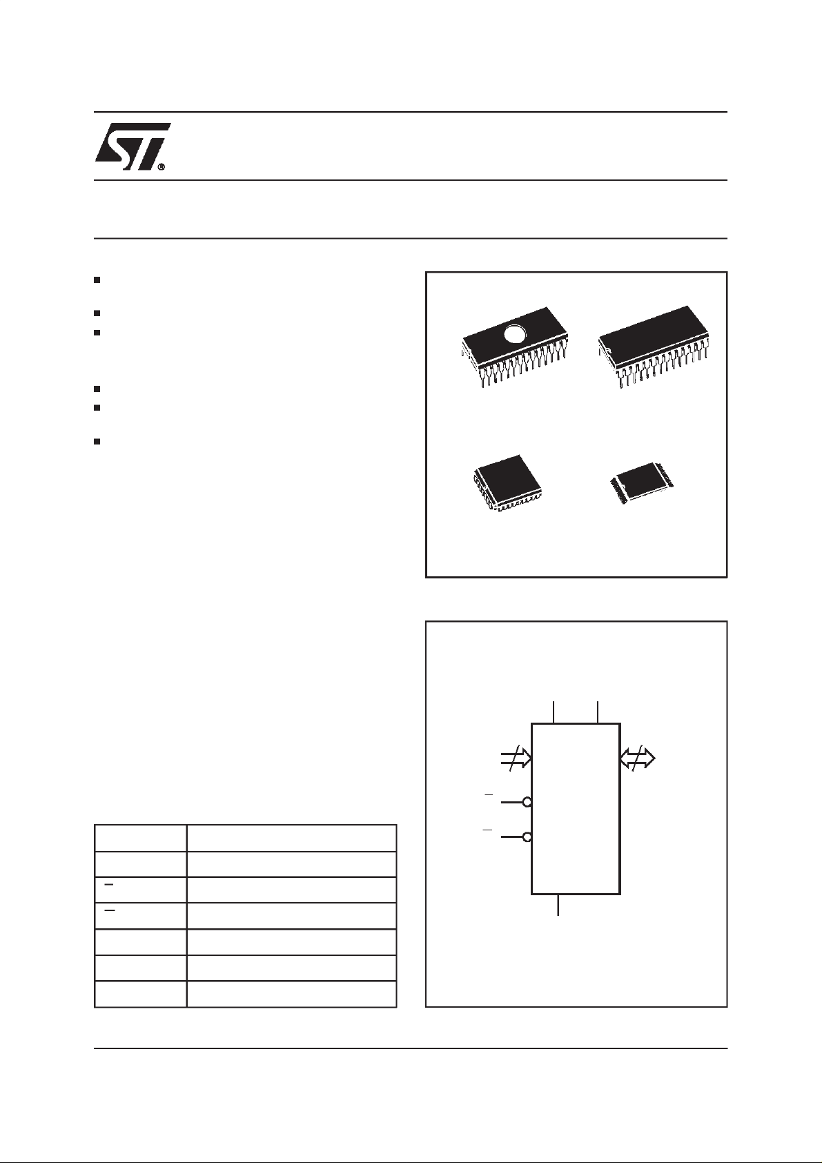
256 Kbit (32Kb x 8) UV EPROM and OTP EPROM
5V ± 10% SUPPLYVOLTAGEin READ
OPERATION
FASTACCESSTIME: 45ns
LOW POWERCONSUMPTION:
– ActiveCurrent 30mAat 5MHz
– StandbyCurrent 100µA
PROGRAMMING VOLTAGE:12.75V ± 0.25V
PROGRAMMINGTIME: 100µs/byte
(PRESTOII ALGORITHM)
ELECTRONICSIGNATURE
– ManufacturerCode:20h
– DeviceCode: 8Dh
28
1
FDIP28W (F)
M27C256B
28
1
PDIP28 (B)
DESCRIPTION
TheM27C256Bisa256 KbitEPROMofferedin the
two ranges UV (ultra violet erase) and OTP (one
time programmable). It is ideally suited for microprocessorsystems and is organizedas 32,768 by
8 bits.
The FDIP28W(window ceramicfrit-seal package)
has a transparent lid which allows the user to
expose the chipto ultravioletlight to erase the bit
pattern. A new pattern can then be written to the
deviceby followingthe programmingprocedure.
Forapplicationswhere the content isprogrammed
only one time and erasure is not required, the
M27C256B is offered in PDIP32, PLCC32 and
TSOP28(8 x 13.4mm) packages.
Table1. Signal Names
A0-A14 Address Inputs
Q0-Q7 Data Outputs
E Chip Enable
G Output Enable
V
PP
Program Supply
PLCC32 (C)
TSOP28 (N)
8 x 13.4mn
Figure1. Logic Diagram
V
15
A0-A14 Q0-Q7
E
G
V
CC
M27C256B
V
PP
SS
8
AI00755B
V
CC
V
SS
July 1998 1/15
Supply Voltage
Ground
Page 2
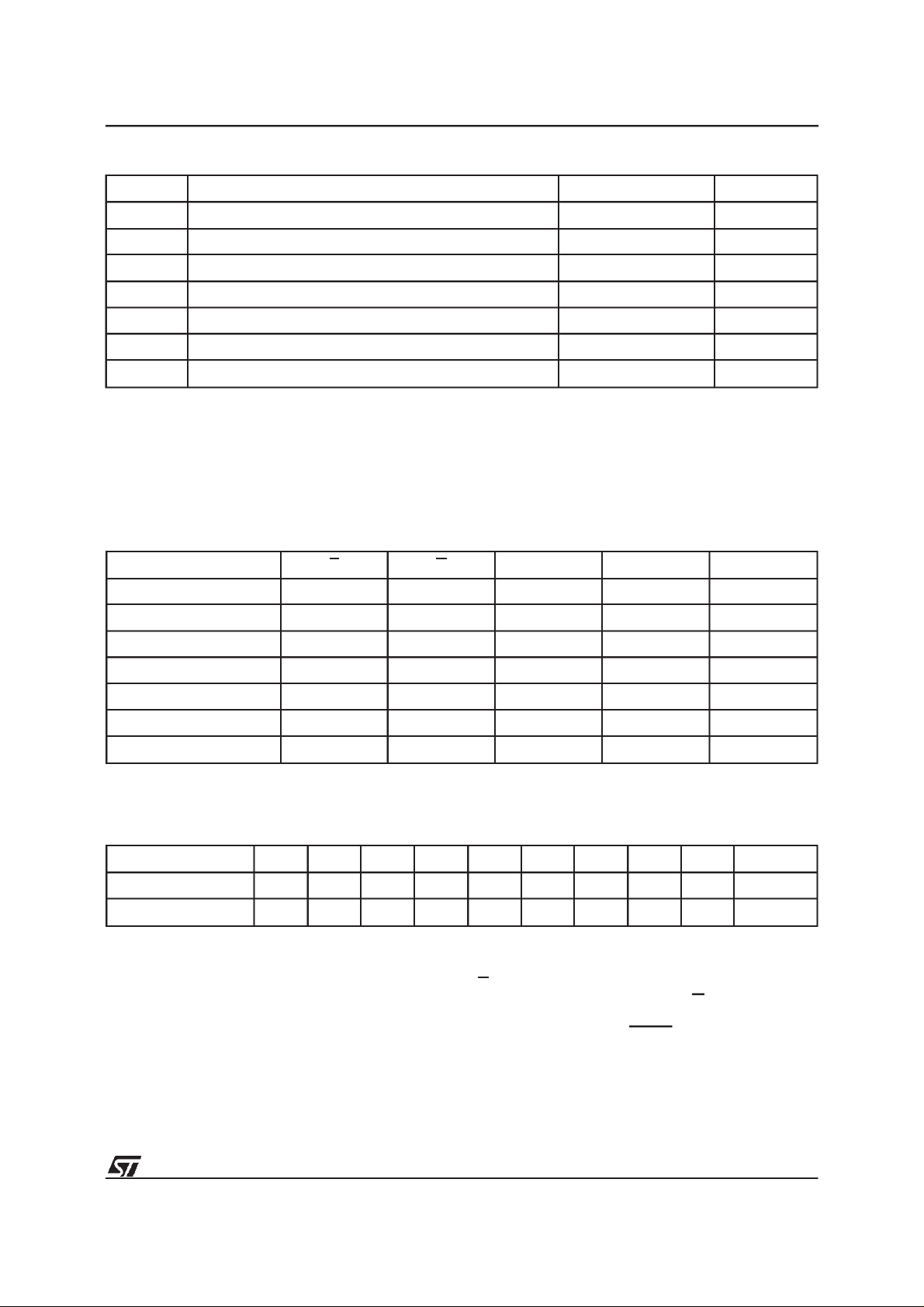
M27C256B
Figure2A. DIPPin Connections
V
PP
A12
A7
A6
A5
A4
A3
A2
A1
A0
Q0
Q2
SS
1
2
3
4
5
6
7
M27C256B
8
9
10
11
12
13
14
28
27
26
25
24
23
22
21
20
19
18
17
16
15
AI00756
V
CC
A14
A13
A8
A9
A11
G
A10
E
Q7
Q6
Q5Q1
Q4
Q3V
Figure2B. LCC PinConnections
PP
CC
A13
DU
32
DU
V
Q3
A14
Q4
25
Q5
A8
A9
A11
NC
G
A10
E
Q7
Q6
AI00757
V
A7
A12
A6
A5
A4
A3
A2
9
A1
A0
NC
Q0
Q1
Warning: NC = Not Connected, DU = Dont’t Use.
1
M27C256B
17
Q2
SS
V
Figure2C. TSOPPin Connections
G
A11
A13
A14
V
V
A12
A9
A8
CC
PP
A7
A6
A5
A4
A3
22
28
M27C256B
1
78
21
15
14
AI00614B
A10
E
Q7
Q6
Q5
Q4
Q3
V
SS
Q2
Q1
Q0
A0
A1
A2
DEVICEOPERATION
The operating modes of the M27C256B are listed
in the Operating Modes. A single power supply is
requiredinthereadmode. AllinputsareTTLlevels
exceptforV
and12V on A9for ElectronicSigna-
PP
ture.
Read Mode
The M27C256Bhas two control functions,both of
which must be logically active in order to obtain
data at the outputs.Chip Enable (E) is the power
control and should be used for device selection.
OutputEnable(G) is theoutputcontrol and should
be used to gate data to the output pins, independent of device selection. Assuming that the
addresses are stable, the address access time
)isequaltothedelayfromE tooutput(t
(t
AVQV
Datais available at the output after delay of t
ELQV
GLQV
from the falling edge of G, assuming that E has
been low and the addresses have been stable for
at leastt
AVQV-tGLQV
.
StandbyMode
The M27C256B has a standby mode which reducesthe supplycurrentfrom 30mAto 100µA.The
M27C256Bis placed in the standby mode by applyinga CMOShigh signal to the E input.When in
thestandbymode,theoutputs are ina highimpedance state,independentof theG input.
).
2/15
Page 3
M27C256B
Table2. AbsoluteMaximum Ratings
(1)
Symbol Parameter Value Unit
T
A
T
BIAS
T
STG
V
IO
V
CC
V
A9
V
PP
Notes: 1. Except for the rating ”Operating Temperature Range”, stresses above those listed in the Table ”Absolute Maximum Ratings”
2. Minimum DC voltage on Input or Output is –0.5V withpossible undershoot to –2.0V for a period less than 20ns. Maximum DC
3. Depends on range.
Ambient Operating Temperature
TemperatureUnder Bias –50 to 125
Storage Temperature –65 to 150
(2)
Input or Output Voltages(except A9) –2 to 7 V
Supply Voltage –2 to 7 V
(2)
A9 Voltage –2 to 13.5 V
Program SupplyVoltage –2 to 14 V
may cause permanent damage to the device. These are stress ratingsonly and operation of the device at these or any other
conditions above those indicated in the Operating sections of this specificationis not implied. Exposure to Absolute Maximum
Rating conditions for extended periods may affectdevice reliability. Refer also tothe STMicroelectronics SURE Program and other
relevant quality documents.
voltage on Output is V
+0.5V with possible overshoot to VCC+2V for a period less than20ns.
CC
(3)
–40 to 125
C
°
C
°
C
°
Table3. Operating Modes
Mode E G A9 V
Read V
Output Disable V
Program V
Verify V
Program Inhibit V
Standby V
Electronic Signature V
Note:X =VIHor VIL,VID= 12V±0.5V
IL
IL
Pulse V
IL
IH
IH
IH
IL
PP
V
IL
V
IH
IH
V
IL
V
IH
XVCCData Out
XVCCHi-Z
XVPPData In
XVPPData Out
XVPPHi-Z
XXVCCHi-Z
V
IL
V
ID
V
CC
Q0 - Q7
Codes
Table4. Electronic Signature
Identifier A0 Q7 Q6 Q5 Q4 Q3 Q2 Q1 Q0 Hex Data
Manufacturer’s Code V
Device Code V
IL
IH
Two Line OutputControl
BecauseEPROMsareusuallyusedin largermemory arrays, this product features a 2 line control
functionwhich accommodatesthe use of multiple
memory connection. The two line control function
allows:
a. the lowest possiblememory power dissipation,
b. complete assurancethat output bus contention
00100000 20h
10001101 8Dh
Forthe mostefficientuse of thesetwocontrollines,
E should be decoded and used as the primary
deviceselectingfunction, whileG shouldbe made
a common connection to all devices in the array
and connected to the READ line from the system
controlbus.Thisensuresthat all deselectedmemory devices are in their low power standby mode
and that the outputpins are only active when data
is desired from a particular memorydevice.
will not occur.
3/15
Page 4
M27C256B
Table5. AC MeasurementConditions
High Speed Standard
Input Rise and Fall Times
Input Pulse Voltages 0 to 3V 0.4V to 2.4V
Input and Output Timing Ref. Voltages 1.5V 0.8V and2V
≤
10ns
≤
20ns
Figure3. AC TestingInput Output Waveform
High Speed
3V
1.5V
0V
Standard
2.4V
0.4V
Table6. Capacitance
Symbol Parameter Test Condition Min Max Unit
C
IN
C
OUT
Note: 1. Sampled only, not 100% tested.
(1)
(TA=25°C, f =1 MHz)
Input Capacitance VIN=0V 6 pF
Output Capacitance V
2.0V
0.8V
AI01822
Figure4. AC TestingLoad Circuit
1.3V
1N914
3.3kΩ
DEVICE
UNDER
TEST
C
L
CL= 30pF for High Speed
CL= 100pFfor Standard
CLincludes JIG capacitance
=0V 12 pF
OUT
OUT
AI01823B
SystemConsiderations
The power switching characteristics of Advance
CMOS EPROMsrequire careful decoupling of the
devices. The supply current, I
, has three seg-
CC
ments that are of interest to thesystem designer:
the standby current level, the active current level,
and transient current peaks that are produced by
thefalling and risingedgesof E. Themagnitudeof
this transient current peaks is dependent on the
capacitiveandinductiveloadingofthe deviceat the
output.
4/15
The associated transient voltage peaks can be
suppressed by complying with the two line output
control and by properly selected decoupling capacitors. It is recommended that a 0.1µF ceramic
capacitor be used on every device between V
CC
andVSS. Thisshould bea highfrequencycapacitor
of low inherent inductance and should be placed
as close to the device as possible. In addition, a
4.7µF bulk electrolytic capacitor should be used
betweenV
and VSSforeveryeight devices.The
CC
bulk capacitor should be located near the power
supply connection point. The purpose of the bulk
capacitoris to overcome the voltage drop caused
by the inductiveeffects of PCB traces.
Page 5
M27C256B
Table7. Read Mode DC Characteristics
(1)
(TA=0 to 70°C, –40 to 85°C, –40 to 105°C or –40 to 125°C; VCC=5V±5% or 5V± 10%;VPP=VCC)
Symbol Parameter Test Condition Min Max Unit
I
LI
I
LO
I
CC
I
CC1
I
CC2
I
PP
V
V
IH
V
OL
V
OH
Notes: 1. VCCmust be applied simultaneouslywith or before VPPand removed simultaneously or after VPP.
Input Leakage Current 0V≤V
Output Leakage Current 0V≤V
Supply Current
E=V
= 0mA, f = 5MHz
I
OUT
Supply Current (Standby) TTL E = V
Supply Current(Standby) CMOS E > VCC– 0.2V 100
Program Current VPP=V
Input Low Voltage –0.3 0.8 V
IL
(2)
Input High Voltage 2 VCC+1 V
Output Low Voltage IOL= 2.1mA 0.4 V
Output High Voltage TTL IOH= –1mA 3.6 V
Output High Voltage CMOS I
2. Maximum DC voltage on Outputis V
CC
+0.5V.
OH
V
≤
IN
CC
V
≤
OUT
CC
,G=VIL,
IL
IH
CC
= –100µAV
– 0.7 V
CC
10
±
10
±
µ
µ
30 mA
1mA
µ
100
µ
A
A
A
A
Table8A. ReadMode AC Characteristics
(1)
(TA=0 to 70°C, –40 to 85°C, –40 to 105°C or –40 to 125°C; VCC=5V±5% or 5V± 10%;VPP=VCC)
M27C256B
Symbol Alt Parameter Test Condition
t
AVQVtACC
t
ELQV
t
GLQV
(2)
t
EHQZ
(2)
t
GHQZ
t
AXQX
Notes: 1. VCCmust be applied simultaneously with or before VPPand removed simultaneously or afterVPP.
2. Sampled only,not 100% tested.
3. In caseof 45ns speed see High Speed ACmeasurement conditions.
Address Validto
Output Valid
Chip Enable Low to
t
CE
Output Valid
Output Enable Low
t
OE
to Output Valid
Chip Enable High to
t
DF
Output Hi-Z
Output Enable High
t
DF
to Output Hi-Z
Address Transition to
t
OH
Output Transition
E=V
G=V
G=V
E=V
,G=V
IL
E=V
E=V
,G=V
IL
IL
IL
IL
IL
IL
IL
(3)
-45
-60 -70 -80
Min Max Min Max Min Max Min Max
45 60 70 80 ns
45 60 70 80 ns
25 30 35 40 ns
0 25 0 30 0 30 0 30 ns
0 25 0 30 0 30 0 30 ns
0000ns
Unit
5/15
Page 6

M27C256B
Table8B. ReadMode AC Characteristics
(1)
(TA=0 to 70°C, –40 to 85°C, –40 to 105°C or –40 to 125°C; VCC=5V±5% or 5V± 10%;VPP=VCC)
M27C256B
Symbol Alt Parameter TestCondition
-90 -10 -12 -15/-20/-25
Min Max Min Max Min Max Min Max
t
AVQVtACC
t
ELQV
t
GLQV
(2)
t
EHQZ
(2)
t
GHQZ
t
AXQX
Notes: 1. VCCmust be applied simultaneously with or before VPPand removed simultaneously or afterVPP.
2. Sampled only,not 100% tested.
Address Validto
Output Valid
Chip Enable Low to
t
CE
Output Valid
Output Enable Low to
t
OE
Output Valid
Chip Enable High to
t
DF
Output Hi-Z
Output Enable High
t
DF
to Output Hi-Z
Address Transition to
t
OH
Output Transition
E=V
E=V
,G=V
IL
G=V
E=V
G=V
E=V
,G=V
IL
IL
IL
IL
IL
IL
IL
90 100 120 150 ns
90 100 120 150 ns
40 50 60 65 ns
0 30 0 30 0 40 0 50 ns
0 30 0 30 0 40 0 50 ns
0000ns
Figure5. Read Mode ACWaveforms
Unit
A0-A14
E
G
Q0-Q7
VALID
tAVQV
tGLQV
tELQV
Programming
When delivered (and after each erasure for UV
EPROM), all bits of the M27C256B are in the ”1”
state. Data is introduced by selectively programming ”0”s into the desired bit locations. Although
only ”0”s will be programmed, both ”1”s and ”0”s
can be present in thedata word. The only way to
VALID
tAXQX
tEHQZ
tGHQZ
Hi-Z
AI00758B
changea ’0’toa ’1’isbydie expositionto ultraviolet
light (UV EPROM). The M27C256B is in the programmingmode when V
at V
and E is pulsed to VIL. The data to be
IH
inputis at12.75V,G is
PP
programmed is applied to 8 bits in parallel to the
data output pins. The levels required for the addressand data inputs areTTL. V
is specifiedto
CC
be 6.25 V ± 0.25V.
6/15
Page 7

M27C256B
Table9. ProgrammingMode DC Characteristics
(1)
(TA=25°C; VCC=6.25V ± 0.25V;VPP=12.75V ± 0.25V)
Symbol Parameter TestCondition Min Max Unit
I
LI
I
CC
I
PP
V
V
V
OL
V
OH
V
Note: 1. VCCmust be applied simultaneouslywith or before VPPand removed simultaneously or after VPP.
Input Leakage Current V
Supply Current 50 mA
Program Current E= V
Input Low Voltage –0.3 0.8 V
IL
Input High Voltage 2 VCC+ 0.5 V
IH
Output Low Voltage IOL= 2.1mA 0.4 V
Output High Voltage TTL IOH= –1mA 3.6 V
A9 Voltage 11.5 12.5 V
ID
Table10. ProgrammingMode AC Characteristics
V
V
≤
≤
IL
IN
IH
IL
(1)
10
±
50 mA
(TA=25°C; VCC=6.25V ± 0.25V;VPP=12.75V ± 0.25V)
Symbol Alt Parameter Test Condition Min Max Unit
t
AVEL
t
Address Valid to Chip Enable Low 2 µs
AS
A
µ
t
QVEL
t
VPHEL
t
VCHEL
t
ELEH
t
EHQX
t
QXGL
t
GLQV
t
GHQZ
t
GHAX
Note: 1. VCCmust be applied simultaneouslywith or before VPPand removed simultaneously or after VPP.
t
t
VPS
t
VCS
t
t
t
OES
t
t
DFP
t
Input Validto Chip Enable Low 2 µs
DS
VPPHigh to Chip Enable Low 2 µs
VCCHigh to Chip Enable Low 2 µs
Chip Enable Program Pulse Width 95 105 µs
PW
Chip Enable High to Input Transition 2 µs
DH
Input Transitionto Output Enable Low 2 µs
Output Enable Low to Output Valid 100 ns
OE
Output Enable High to Output Hi-Z 0 130 ns
Output Enable High to AddressTransition 0 ns
AH
7/15
Page 8

M27C256B
Figure6. Programmingand VerifyModes AC Waveforms
A0-A14
tAVEL
Q0-Q7
V
PP
V
CC
E
G
DATA IN DATA OUT
tQVEL
tVPHEL
tVCHEL
tELEH
Figure7. ProgrammingFlowchart
VCC= 6.25V, VPP= 12.75V
n=0
E = 100µs Pulse
NO
NO
VERIFY
YES
Last
NO
Addr
YES
CHECK ALL BYTES
1st: VCC=6V
2nd: VCC= 4.2V
++ Addr
YES
++n
=25
FAIL
VALID
tEHQX
tGLQV
tQXGL
PROGRAM VERIFY
PRESTOII ProgrammingAlgorithm
PRESTOII ProgrammingAlgorithmallows to programthe wholearray with a guaranteedmargin,in
a typical time of 3.5 seconds. Programming with
PRESTOII involvesthe applicationof a sequence
of100µsprogrampulsestoeachbyteuntilacorrect
verifyoccurs (see Figure 7). During programming
and verify operation, a MARGIN MODE circuit is
automatically activated in order to guarantee that
each cell is programmedwith enoughmargin. No
overprogram pulse is applied since the verify in
MARGIN MODE provides necessary margin to
each programmedcell.
ProgramInhibit
Programming of multiple M27C256Bs in parallel
with different data is also easily accomplished.
Except for E, all like inputs including G of the
parallel M27C256B may be common. ATTL low
level pulse applied to a M27C256B’sE input,with
at 12.75 V, will program that M27C256B. A
V
PP
high level E input inhibits the other M27C256Bs
frombeingprogrammed.
ProgramVerify
AI00760B
A verify (read) should be performed on the programmedbits todeterminethattheywere correctly
programmed. Theverifyis accomplishedwith Gat
, E at VIH,VPPat 12.75V and VCCat 6.25V.
V
IL
tGHQZ
tGHAX
AI00759
8/15
Page 9

M27C256B
On-BoardProgramming
TheM27C256Bcan bedirectly programmedin the
application circuit. See the relevant Application
NoteAN620.
ElectronicSignature
The Electronic Signature (ES) mode allows the
reading outof abinary code from an EPROMthat
will identify its manufacturerand type. This mode
is intended for use by programming equipment to
automaticallymatchthe deviceto be programmed
withits correspondingprogrammingalgorithm.The
ES mode is functionalin the 25°C ± 5°C ambient
temperaturerange that is required when programmingthe M27C256B.Toactivatethe ESmode,the
programmingequipmentmustforce11.5Vto 12.5V
on addressline A9 of the M27C256B, with V
V
= 5V. Two identifier bytes may then be se-
PP
CC
quenced from the device outputs by toggling addresslineA0fromV
must be held at V
mode. Byte 0 (A0=V
turercodeand byte1 (A0=V
toVIH. Allotheraddresslines
IL
during Electronic Signature
IL
) represents the manufac-
IL
) thedeviceidentifier
IH
code. For the STMicroelectronics M27C256B,
thesetwo identifier bytes are givenin Table4 and
canbe read-outon outputsQ0 to Q7.
ERASURE OPERATION(appliesfor UV EPROM)
The erasure characteristics of the M27C256B is
such that erasure begins when the cells are exposed to light with wavelengths shorter than approximately4000 Å.It shouldbe notedthatsunlight
and some type of fluorescent lamps have wavelengthsin the3000-4000Årange.Researchshows
that constant exposure to room level fluorescent
lighting could erasea typicalM27C256B in about
3 years, while it would take approximately1 week
to cause erasure when exposedto directsunlight.
If the M27C256B is to be exposed to these types
of lightingconditions for extendedperiods of time,
it is suggestedthat opaque labels be put over the
M27C256B window to prevent unintentional erasure.The recommendederasureprocedureforthe
=
M27C256B is exposure to short wave ultraviolet
light which haswavelength 2537Å.The integrated
dose(i.e. UVintensityx exposuretime)forerasure
should be a minimum of 15 W-sec/cm
sure time with this dosage is approximately15 to
20 minutes using an ultraviolet lamp with 12000
µW/cm
2
power rating. The M27C256B should be
placed within 2.5 cm (1 inch) of the lamp tubes
during the erasure. Some lamps have a filter on
their tubes which should be removed before erasure.
2
. The era-
9/15
Page 10

M27C256B
ORDERING INFORMATION SCHEME
Example: M27C256B -70 X C 1 TR
Speed
(1)
-45
-60 60 ns
-70 70 ns
-80 80 ns
-90 90 ns
-10 100 ns
-12 120 ns
-15 150 ns
-20 200 ns
-25 250 ns
Note: 1. High Speed,see AC Characteristics section for further information.
45 ns
V
Tolerance
CC
X ± 5%
blank
±
10%
Package
F FDIP28W
B PDIP28
C PLCC32
N TSOP28
8 x 13.4mm
Temperature Range
1 0 to 70 °C
6 –40 to 85°C
7 –40 to 105°C
3 –40 to 125°C
Option
X Additional
Burn-in
TR Tape& Reel
Packing
Fora listofavailableoptions(Speed,Package,etc...)or forfurtherinformationon anyaspectof thisdevice,
pleasecontact the STMicroelectronicsSales Officenearest to you.
10/15
Page 11

FDIP28W - 28 pin CeramicFrit-seal DIP, with window
M27C256B
Symb
A 5.71 0.225
A1 0.50 1.78 0.020 0.070
A2 3.90 5.08 0.154 0.200
B 0.40 0.55 0.016 0.022
B1 1.17 1.42 0.046 0.056
C 0.22 0.31 0.009 0.012
D 38.10 1.500
E 15.40 15.80 0.606 0.622
E1 13.05 13.36 0.514 0.526
e1 2.54 – – 0.100 – –
e3 33.02 – – 1.300 – –
eA 16.17 18.32 0.637 0.721
L 3.18 4.10 0.125 0.161
S 1.52 2.49 0.060 0.098
∅
α
N28 28
Typ Min Max Typ Min Max
7.11 – – 0.280 – –
mm inches
4
°
15
°
4
°
15
°
Drawing is not to scale.
A2
B1 B e
D2
D
S
N
1
A3A1A
L
α
C
eA
eB
∅
E1 E
FDIPW-a
11/15
Page 12

M27C256B
PDIP28 - 28 pin Plastic DIP, 600 mils width
Symb
Typ Min Max Typ Min Max
A – 5.08 – 0.200
A1 0.38 – 0.015 –
A2 3.56 4.06 0.140 0.160
B 0.38 0.51 0.015 0.020
B1 1.52 – – 0.060 – –
C 0.20 0.30 0.008 0.012
D 36.83 37.34 1.450 1.470
D2 33.02 – – 1.300 – –
E 15.24 – – 0.600 – –
E1 13.59 13.84 0.535 0.545
e1 2.54 – 0.100 – –
eA 14.99 – 0.590 – –
eB 15.24 17.78 0.600 0.700
L 3.18 3.43 0.125 0.135
S 1.78 2.08 0.070 0.082
α
N28 28
mm inches
0
°
10
°
0
°
10
°
Drawing is notto scale.
12/15
B1 B e1
D2
D
S
N
1
A2A1A
E1 E
L
α
C
eA
eB
PDIP
Page 13

PLCC32 - 32lead Plastic Leaded Chip Carrier- rectangular
M27C256B
Symb
Typ Min Max Typ Min Max
A 2.54 3.56 0.100 0.140
A1 1.52 2.41 0.060 0.095
A2 – 0.38 – 0.015
B 0.33 0.53 0.013 0.021
B1 0.66 0.81 0.026 0.032
D 12.32 12.57 0.485 0.495
D1 11.35 11.56 0.447 0.455
D2 9.91 10.92 0.390 0.430
E 14.86 15.11 0.585 0.595
E1 13.89 14.10 0.547 0.555
E2 12.45 13.46 0.490 0.530
e 1.27 – – 0.050 – –
F 0.00 0.25 0.000 0.010
R 0.89 – – 0.035 – –
N32 32
Nd 7 7
Ne 9 9
CP 0.10 0.004
mm inches
D
D1
1N
Ne E1 E
Nd
PLCC
Drawing is not to scale.
R
F
0.51 (.020)
1.14 (.045)
D2/E2
A1
A2
B1
e
B
A
CP
13/15
Page 14

M27C256B
TSOP28- 28 lead Plastic Thin Small Outline, 8 x 13.4mm
Symb
Typ Min Max Typ Min Max
A 1.00 1.25 0.039 0.049
A1 0.20 0.008
A2 0.95 1.05 0.037 0.041
B 0.30 0.012
C 0.10 0.21 0.004 0.008
D 13.10 13.70 0.516 0.539
D1 11.70 11.90 0.461 0.469
E 7.90 8.25 0.311 0.325
e 0.55 - - 0.022 - -
L 0.30 0.70 0.012 0.028
α
N28 28
CP 0.10 0.004
mm inches
0
°
5
°
0
°
5
°
Drawing is notto scale.
28
1
22
21
E
78
D1
D
DIE
TSOP-c
A2
e
B
A
CP
C
LA1 α
14/15
Page 15

M27C256B
Information furnished is believed to be accurate and reliable. However, STMicroelectronics assumes no responsibility for the consequences
ofuse ofsuch information nor for any infringement of patents or other rights of third parties which may resultfrom itsuse. No license is granted
by implicationor otherwiseunder any patent or patent rights of STMicroelectronics. Specifications mentioned in this publicationare subject to
change without notice. This publication supersedes and replaces all information previously supplied. STMicroelectronics products are not
authorized for use as criticalcomponents in life support devices or systems without express written approval of STMicroelectronics.
The ST logo is a registeredtrademark of STMicroelectronics
1998 STMicroelectronics - All Rights Reserved
Australia - Brazil - China - France - Germany -Italy - Japan - Korea - Malaysia - Malta - Mexico - Morocco - TheNetherlands -
Singapore - Spain - Sweden- Switzerland - Taiwan - Thailand - United Kingdom - U.S.A.
STMicroelectronics GROUP OF COMPANIES
15/15
 Loading...