

Page 1
查询M27C160-100F1供应商
16 Mbit (2Mb x 8 or 1Mb x 16) UV EPROM and OTP EPROM
■ 5V ± 10% SUPPLY VOLTAGE in READ
OPERATION
■ ACCESS TIME: 50ns
■ BYTE-WID E or WORD-WIDE
CONFIGURABLE
■ 16 Mbit MASK ROM REPLACEMENT
■ LOW P OWER CONSUMPTION
– Active Current 70mA at 8MHz
– Standby Current 100µA
■ PROGRAMMING VOLTAGE: 12.5V ± 0.25V
■ PROG RAMM ING T IME: 50µs/word
■ ELECTRONIC SIGNATURE
– Manufacturer Code: 20h
– Device Code: B1h
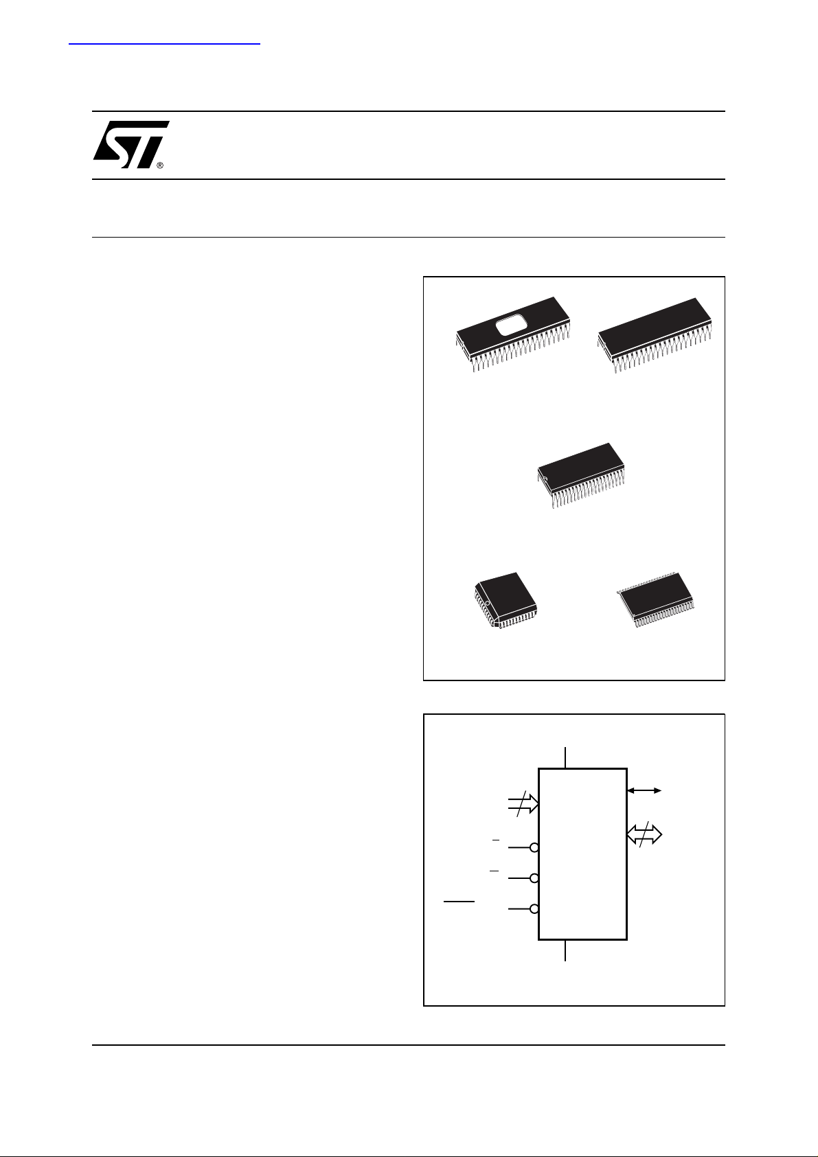
42
1
FDIP42W (F)
M27C160
42
1
PDIP42 (B)
42
1
SDIP42 (S)
DESCRIPTION
The M27C160 is a 16 Mbit EPROM offered in the
two ranges UV (ultra violet erase) and OTP ( one
time programmable). It is ideally suited for microprocessorsystemsrequiringlarge data or program
storage and is organised as either 2 Mb it words of
8 bit or 1 Mbit words of 16 bit. The pin-out is compatible with a 16 Mbit Mask ROM.
The FDIP42W (window ceramic frit-seal package)
has a transparent lid whi ch allows the user to expose the chip to ultraviolet light to erase the bit pattern. A new pattern can then be written rapidly to
the device by following the p rogramm ing procedure.
For applications where the content is programmed
only one time and erasure is not required, the
M27C160 is offered in PDIP42, SDIP42, PLCC44
and SO44 packages.
PLCC44 (K)
Figure 1. Logic Diagram
V
CC
20
A0-A19
BYTEV
E
G
PP
M27C160
V
SS
44
1
SO44 (M)
Q15A–1
15
Q0-Q14
AI00739B
1/19January 2002
Page 2
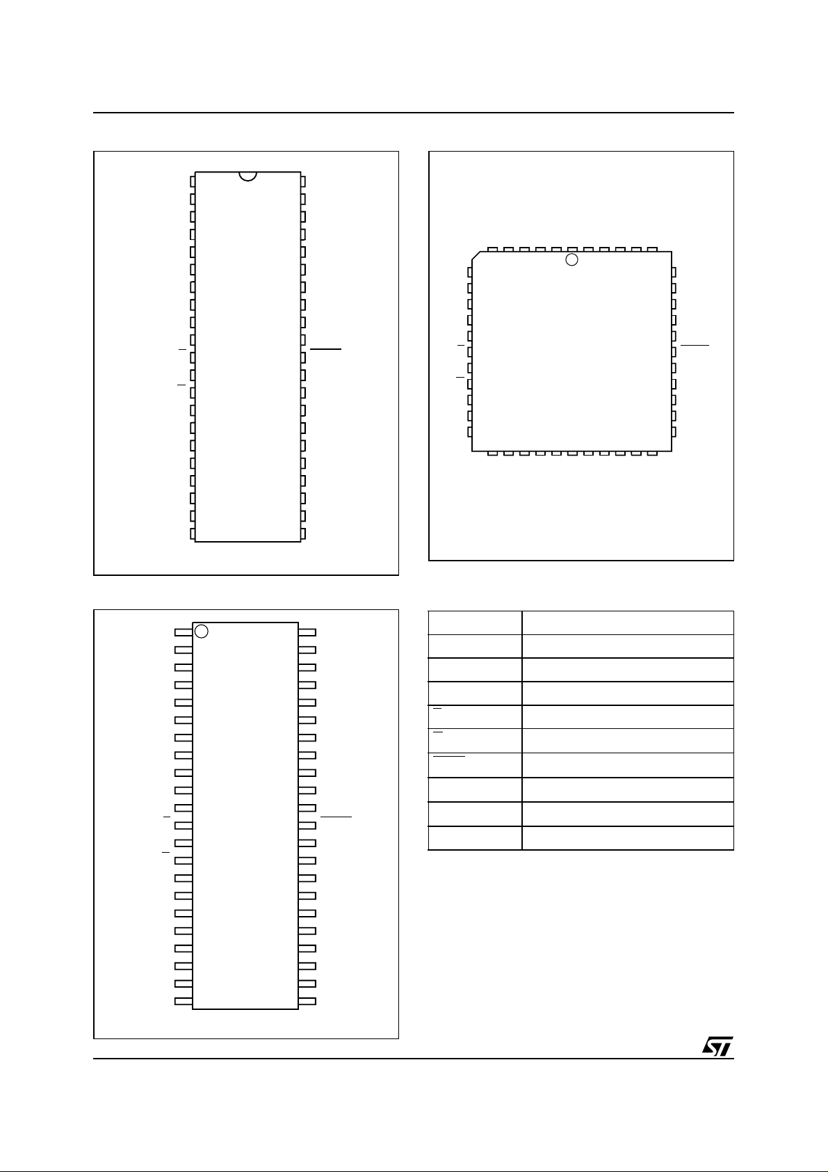
M27C160
Figure 2. DIP Connections
A18 A19
1
2
A7
3
4
A6
5
A5
A4
6
7
A3
A2
8
A1
9
10
A0
V
SS
Q0
Q8
Q1
Q9
Q10
Q3
Q11
E
G
11
12
13
14
15
16
17
18
19
20
21
M27C160
42
41
40
39
38
37
36
35
34
33
32
31
30
29
28
27
26
25
24
23
22
AI00740
A8A17
A9
A10
A11
A12
A13
A14
A15
A16
BYTEV
V
SS
Q15A-1
Q7
Q14
Q6
Q13
Q5Q2
Q12
Q4
V
CC
PP
Figure 3. PLCC Connections
A18
A17
V
1
M27C160
23
Q3
NC
Q11
SS
44
A19
CC
V
A8
Q4
A9
Q12
A10
Q5
A7
A5
A6
A4
A3
A2
A1 A15
A0
E
12
V
SS
Q0
Q8
Q1
Q9
Q2
Q10
A11
34
Q13
A12
A13
A14
A16
BYTEV
V
SS
Q15A–1G
Q7
Q14
Q6
AI03012
PP
Figure 4. SO Connections
NC NC
A17 A8
V
SS
Q0
Q8
Q9
Q10
Q3
Q11
A7
A6
A5
A4
A3
A2
A1
A0
1
2
3
4
5
6
7
8
9
10
11
M27C160
12
E
13
14
G
15
16
17Q1
18
19
20
21
44
43
42
41
40
39
38
37
36
35
34
33
32
31
30
29
28
27
26
25
24
2322
AI01264
A19A18
A9
A10
A11
A12
A13
A14
A15
A16
BYTEV
V
SS
Q15A-1
Q7
Q14
Q6
Q13
Q5Q2
Q12
Q4
V
CC
PP
Table 1. Signal Names
A0-A19 Address Inputs
Q0-Q7 Data Outputs
Q8-Q14 Data Outputs
Q15A–1 Data Output / Address Input
E
G
BYTE
V
PP
V
CC
V
SS
NC Not Connected Internally
Chip Enable
Output Enable
Byte Mode / Program Supply
Supply Voltage
Ground
2/19
Page 3
M27C160
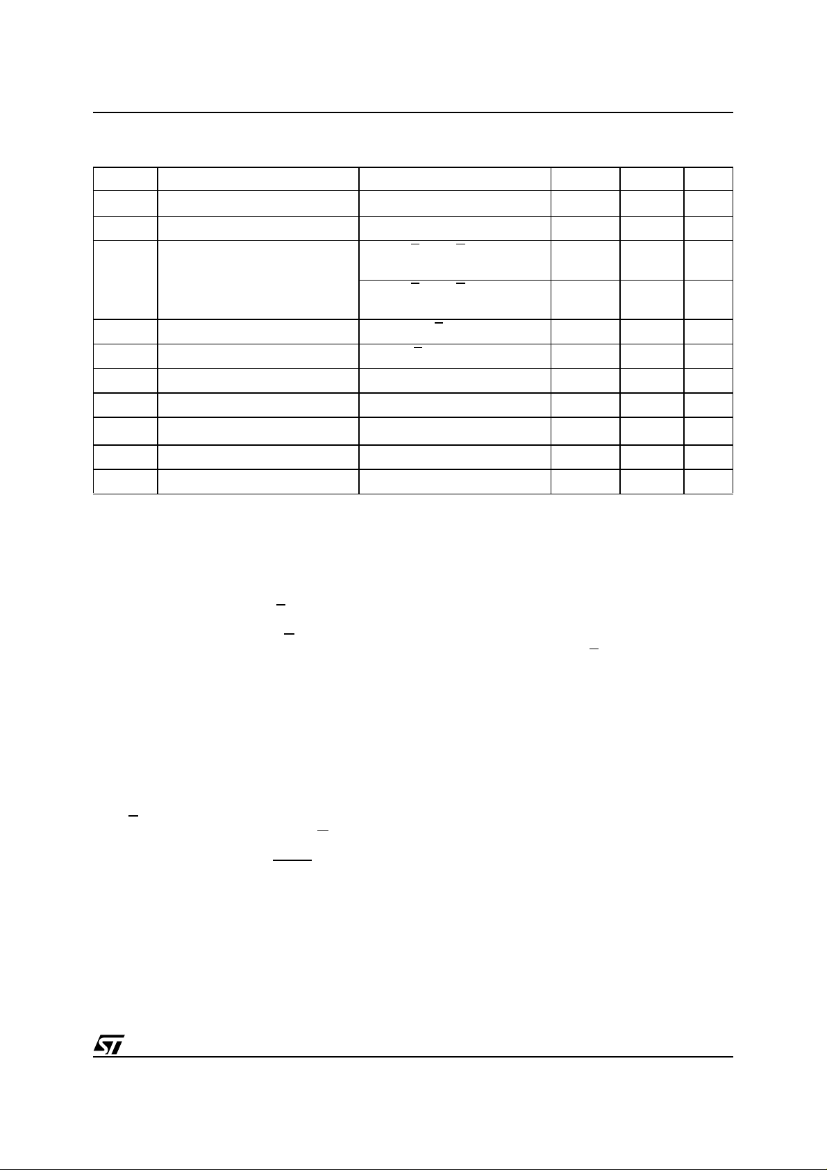
Table 2. Absolute Maximum Ratings
(1)
Symbol Parameter Value Unit
T
A Ambient Operating Temperature
T
BIAS
T
STG
(2)
V
IO
V
CC
(2)
V
A9
V
PP
Note: 1. Except for the rating "Operating Temperature Range", stresses above those listed in the Table "Absolute Maximum Ratings" may
cause permanent damage to the device. These are stress ratings only and operation of the device at these or any other conditions
above those indicated in the Operating sections of this specification is not implied. Exposure to Absolute Maximum Rating conditionsfor extended periods may affectdevice reliability. Referalsoto the STMicroelectronics SUREProgramandother relevant quality documents.
2. Minimum DC voltage on Input or Output is –0.5V with possible undershoot to –2.0V for a period less than 20ns. Maximum DC
voltage on Output is V
3. Depends on range.
Temperature Under Bias –50 to 125 °C
Storage Temperature –65 to 150 °C
Input or Output Voltage (except A9) –2 to 7 V
Supply Voltage –2 to 7 V
A9 Voltage –2 to 13.5 V
Program Supply Voltage –2 to 14 V
+0.5VwithpossibleovershoottoVCC+2V for a period less than 20ns.
CC
(3)
–40 to 125 °C
Table 3. Operating Modes
Mode E
Read Word-wide
Read Byte-wide Upper
Read Byte-wide Lower
Output Disable
Program
V
Verify
Program Inhibit
Standby
Electronic Signature
Note: X = VIHor VIL,VID= 12V ± 0.5V.
V
IL
V
IL
V
IL
V
IL
Pulse V
IL
V
IH
V
IH
V
IH
V
IL
G
V
V
V
V
V
V
X X X Hi-Z Hi-Z Hi-Z
V
BYTEV
PP
IL
IL
IL
IH
IH
IL
IH
IL
V
IH
V
IL
V
IL
X X Hi-Z Hi-Z Hi-Z
V
PP
V
PP
V
PP
V
IH
A9 Q15A–1 Q8-Q14 Q7-Q0
X Data Out Data Out Data Out
X
X
V
IH
V
IL
Hi-Z Data Out
Hi-Z Data Out
X Data In Data In Data In
X Data Out Data Out Data Out
X Hi-Z Hi-Z Hi-Z
V
ID
Code Codes Codes
Table 4. Electronic Signature
Identifier A0 Q7 Q6 Q5 Q4 Q3 Q2 Q1 Q0 Hex Data
Manufacturer’s Code
Device Code
Note: Outputs Q15-Q8 are set to '0'.
V
V
IL
IH
00100000 20h
10110001 B1h
3/19
Page 4
M27C160
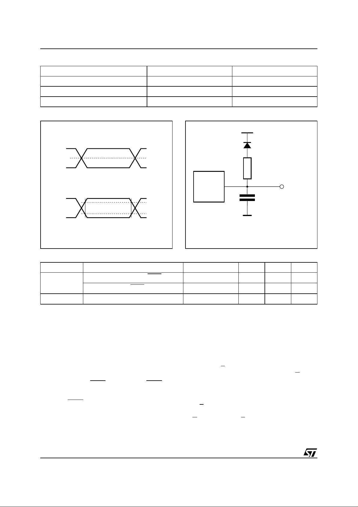
Table 5. AC M easurement Conditions
High Speed Standard
Input Rise and Fall Times ≤ 10ns ≤ 20ns
Input Pulse Voltages 0 to 3V 0.4V to 2.4V
Input and Output Timing Ref. Voltages 1.5V 0.8V and 2V
Figure 5. AC Testing Input Output Waveform
High Speed
3V
1.5V
0V
Standard
2.4V
0.4V
Table 6. Capacitance
Symbol Parameter Test Condition Min Max Unit
C
IN
C
OUT
Note: 1. Sampled only, not 100% tested.
(1)
(TA=25°C,f=1MHz)
Input Capacitance (except BYTEVPP)V
Input Capacitance (BYTE
Output Capacitance
2.0V
0.8V
AI01822
VPP)V
Figure 6. AC Testing Load Circuit
1.3V
1N914
3.3kΩ
DEVICE
UNDER
TEST
CL
CL = 30pF for High Speed
CL = 100pF for Standard
CL includes JIG capacitance
V
IN
IN
OUT
=0V
=0V
=0V
10 pF
120 pF
12 pF
OUT
AI01823B
DEVICE OPERATION
The operating modes of the M27C160 are listed in
the Operating Modes Table. A single power supply
is required in the read mode. All inputs are TTL
compatible except for V
and 12V on A9 for the
PP
Electronic Signature.
Read Mode
The M27C160 has two organisations, Word-wide
and Byte-wide. The organisation isselected by the
signal level on the BYTE
VPPpin. When BYTEV
PP
is at VIHthe Word-wide organisation is selected
and the Q15A–1 pin is used for Q15 Data Output.
When the BYTE
VPPpin is at VILthe Byte-wide organisation is selected and the Q15A–1 pin is used
for the Address In put A–1. When the memory is
logically regarded as 16 bit wide, but read in the
Byte-wide organisation, then with A–1 at V
4/19
the
IL
lower 8 bits of the 16 bit data are s elected and with
A–1 at V
the upper 8 bits of the 16 bit data are
IH
selected.
The M27C160 has tw o control func ti ons , both of
which mus t be logically active in order to obtain
data at the outputs. In addition the Word-wide or
Byte- wide organisation must be selected.
ChipEnable (E
used for device selection. Output Enable (G
) is the power control and should be
)isthe
output control and s hould be used to gate data to
the output pins independent of device selection.
Assuming that the addresses are st able, the address access time (t
from E
to output (t
ELQV
output after a delay of t
of G
, assuming that E has been low and the ad-
dresses have been s tab le for at least t
) is equal to the delay
AVQV
). Data is available at the
from the falling edge
GLQV
AVQV-tGLQV
.
Page 5
M27C160
Table 7. Read Mode DC Characteristics
(1)
(TA=0to70°Cor–40to85°C;VCC= 5V ± 5% or 5V ± 10%; VPP=VCC)
Symbol Parameter Test Condition Min Max Unit
I
I
LO
I
CC
I
CC1
I
CC2
I
PP
V
V
IH
V
V
Note: 1. VCCmust be applied simultaneously with or before VPPand removed simultaneously or after VPP.
Input Leakage Current
LI
Output Leakage Current
Supply Current
Supply Current (Standby) TTL
Supply Current (Standby) CMOS
Program Current
Input Low Voltage –0.3 0.8 V
IL
(2)
Input High Voltage 2
Output Low Voltage
OL
Output High Voltage TTL
OH
2. Maximum DC voltage on Output is V
CC
+0.5V.
I
OUT
I
OUT
0V ≤ V
0V ≤ V
E
E
E
I
OH
≤ V
IN
CC
≤ V
OUT
=VIL,G=VIL,
= 0mA, f = 8MHz
=VIL,G=VIL,
= 0mA, f = 5MHz
E
>VCC– 0.2V
V
PP=VCC
I
= 2.1mA
OL
= –400µA
=V
CC
IH
2.4 V
±1 µA
±10 µA
70 mA
50 mA
1mA
100 µA
10 µA
V
+1
CC
0.4 V
V
Standby Mode
The M27C160 has a standby mode which reduces
the active current from 50mA to 100µA. The
M27C160 is placed in the standby mode by applying a CMOS high sig nal to the E
input. When in the
standby mode, the outputs are in a high impedance state, independent of the G
input.
Two Line Output Control
Because EPROMs are usually used in larger
memory arrays, this product features a 2 line control function which accommodates the use of multiple memory connection. The two line control
function allows:
a. the lowest possible memory power dissipation,
b. complete assurance that output bus contention
will not occur.
For the most efficient use of thes e two control
lines, E
ry device selecting function, while G
should be decoded and us ed as theprima-
should be
made a common connection to all devices in the
array and connected to the READ
line from the
system control bus. This ensures that all des elected memory devices are in their low power standby
mode and that the out put pins are only active
when data is required from a partic ular me mory
device.
System Considerations
The power switching characteristics of Advanced
CMOS EPROMs r equire careful decoupling of the
supplies to the de vice s. The supply current I
CC
has three segments of i mportance to the system
designer: t he standby current, the active current
and the transient peaks that a re produced by the
falling and rising edges of E
.
The magnitude of the transient current peak s is
dependent on the c apacitive and i nduc ti ve loading
of the device outputs. The associated trans ient
voltage peaks can be suppressed by compl ying
with th e two line output control and by properly selected decou pling capacitors. It is recommended
that a 0.1µF ceramic capacitor is used on every
device between V
and VSS. This should be a
CC
high frequency type of low inherent inductance
and should be placed as close as possible to the
device. In addition, a 4 .7µ F electrolytic c apacitor
should be used bet ween V
and VSSfor every
CC
eight devices.
This capacitor s hould be mounted near the power
supply connection point. The purpose of this capacitor is to overcome the v olt age drop caused by
the inductive effects of PCB traces.
5/19
Page 6
M27C160
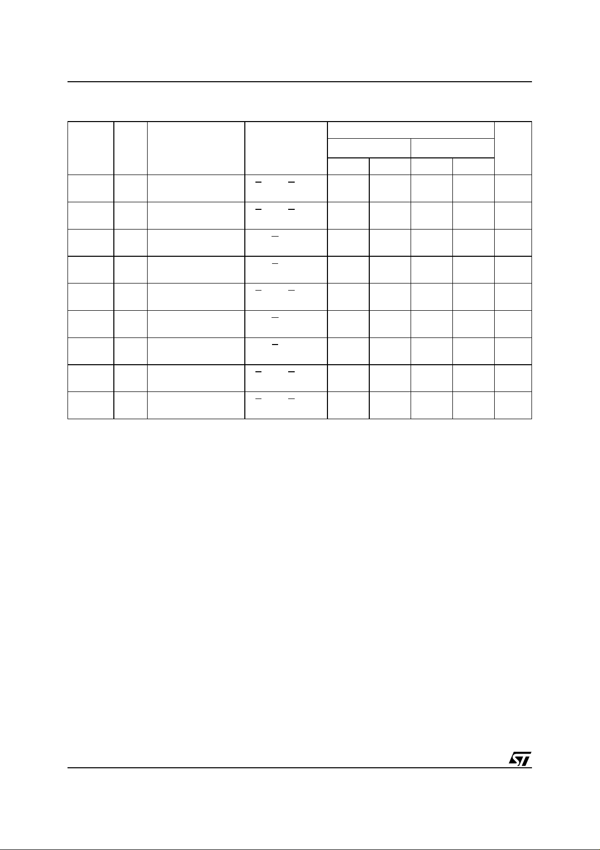
Table 8. Read Mode AC Characteristics
(1)
(TA=0to70°Cor–40to85°C;VCC= 5V ± 5% or 5V ± 10%; VPP=VCC)
M27C160
Symbol Alt Parameter Test Condition
Min Max Min Max
Address Valid to
(2)
(2)
(2)
t
ACC
Output Valid
BYTE High to Output
t
ST
Valid
Chip Enable Low to
t
CE
Output Valid
Output Enable Low to
t
OE
Output Valid
BYTE Low to Output
t
STD
Hi-Z
Chip Enable High to
t
DF
Output Hi-Z
Output Enable High to
t
DF
OutputHi-Z
Address Transition to
t
OH
Output Transition
BYTE Low to
t
OH
Output Transition
t
AVQV
t
BHQV
t
ELQV
t
GLQV
t
BLQZ
t
EHQZ
t
GHQZ
t
AXQX
t
BLQX
Note: 1. VCCmust be applied simultaneously with or before VPPand removed simultaneously or after V
2. Sampled only, not 100% tested.
3. Speed obtained with High Speed AC measurement conditions.
=VIL,G=V
E
=VIL,G=V
E
=V
G
=V
E
=VIL,G=V
E
=V
G
=V
E
=VIL,G=V
E
=VIL,G=V
E
IL
IL
IL
IL
IL
IL
IL
IL
IL
(3)
-50
50 70 ns
50 70 ns
50 70 ns
30 35 ns
30 30 ns
0 25 0 25 ns
0 25 0 25 ns
55ns
55ns
PP.
-70
(3)
Unit
6/19
Page 7

M27C160
Table 9. Read Mode AC Characteristics
(1)
(TA=0to70°Cor–40to85°C;VCC= 5V ± 5% or 5V ± 10%; VPP=VCC)
M27C160
Symbol Alt Parameter Test Condition
Min Max Min Max Min Max
t
AVQVtACC
t
BHQV
t
ELQV
t
GLQV
(2)
t
BLQZ
(2)
t
EHQZ
(2)
t
GHQZ
t
AXQX
Address Valid to
Output Valid
BYTE High to
t
ST
Output Valid
Chip Enable Low to
t
CE
Output Valid
Output Enable Low
t
OE
to Output Valid
BYTE Low to Output
t
STD
Hi-Z
Chip Enable High to
t
DF
Output Hi-Z
Output Enable High
t
DF
to OutputHi-Z
Address Transition
t
OH
to Output Transition
=VIL,G=V
E
=VIL,G=V
E
=V
G
=V
E
=VIL,G=V
E
=V
G
=V
E
=VIL,G=V
E
IL
IL
IL
IL
IL
IL
IL
IL
90 100 120 ns
90 100 120 ns
90 100 120 ns
45 50 60 ns
30 40 50 ns
030040050ns
030040050ns
555ns
Unit-90 -100 -120/-150
t
BLQX
Note: 1. VCCmust be applied simultaneously with or before VPPand removed simultaneously or after V
2. Sampled only, not 100% tested.
3. Speed obtained with High Speed AC measurement conditions.
BYTE Low to
t
OH
Output Transition
=VIL,G=V
E
555ns
IL
Figure 7. Wo rd-Wide Read Mode AC Waveforms
A0-A19
E
G
Q0-Q15
tAVQV
tELQV
VALID
tAXQX
tGLQV
VALID
tEHQZ
tGHQZ
PP.
Hi-Z
AI00741B
Note: BYTEVPP=VIH.
7/19
Page 8

M27C160
Figure 8. Byte-Wide Read Mode AC Waveforms
A–1,A0-A19
E
G
Q0-Q7
Note: BYTEVPP=VIL.
VALID
tAVQV
tGLQV
tELQV
Figure 9. BYTE T ran sition AC Waveforms
A0-A19
VALID
tAXQX
tEHQZ
tGHQZ
Hi-Z
AI00742B
VALID
A–1
tAVQV
BYTEV
PP
Q0-Q7
tBLQX
Q8-Q15
tBLQZ
Note: Chip Enable (E) and Output Enable (G)=VIL.
8/19
VALID
Hi-Z
tAXQX
tBHQV
DATA OUT
DATA OUT
AI00743C
Page 9

M27C160
Table 10. Progr am m ing Mode DC Characteristics
(1)
(TA=25°C;VCC= 6.25V ± 0.25V; VPP= 12.5V ± 0.25V)
Symbol Parameter Test Condition Min Max Unit
I
I
CC
I
PP
V
V
V
V
OH
V
Note: 1. VCCmust be applied simultaneously with or before VPPand removed simultaneously or after VPP.
Input Leakage Current
LI
Supply Current 50 mA
Program Current
Input Low Voltage –0.3 0.8 V
IL
Input High Voltage 2.4
IH
Output Low Voltage
OL
Output High Voltage TTL
A9 Voltage 11.5 12.5 V
ID
Table 11. Progr am m ing Mode AC Characteristics
0 ≤ V
I
OL
I
OH
(1)
E
≤ V
IN
CC
=V
IL
= 2.1mA
= –2.5mA
±1 µA
50 mA
V
+0.5
CC
0.4 V
3.5 V
(TA=25°C;VCC= 6.25V ± 0.25V; VPP= 12.5V ± 0.25V)
Symbol Alt Parameter Test Condition Min Max Unit
t
AVEL
t
QVEL
t
VPHAV
t
VCHAV
t
ELEH
t
EHQX
t
QXGL
t
GLQV
(2)
t
GHQZ
t
GHAX
Note: 1. VCCmust be applied simultaneously with or before VPPand removed simultaneously or after VPP.
2. Sampled only, not 100% tested.
t
t
DS
t
VPS
t
VCS
t
PW
t
DH
t
OES
t
OE
t
DFP
t
AH
Address Valid to Chip Enable Low 2 µs
AS
Input Valid to Chip Enable Low 2 µs
VPPHigh to Address Valid
VCCHigh to Address Valid
2µs
2µs
Chip Enable Program Pulse Width 45 55 µs
Chip Enable High to Input Transition 2 µs
Input Transition to Output Enable Low 2 µs
Output Enable Low to Output Valid 120 ns
Output Enable High to Output Hi-Z 0 130 ns
Output Enable High to Address
Transition
0ns
V
Programming
When delivered (and after each erasure for UV
EPROM), all bits of the M27C160 are in the '1'
state. Data i s introduced by selectively programming '0's into the desired bit locations. Al tho ugh
only '0's will be programmed, both '1's and '0's can
be present in the data wo rd. The only way to
change a '0' to a'1' is by die exposure to ultrav iolet
light (UV E P R OM). T he M27C160 is in t he programming mode when V
at V
and E is pulsed to VIL.Thedatatobepro-
IH
input is at 12.5V, G is
PP
grammed is applied to16 bitsin parallelto t he data
output pins. The levels required for the address
and data inputs are TTL. V
is specified to be
CC
6.25V ± 0.25V.
9/19
Page 10

M27C160
Figure 10. Programming and V erify Modes AC Waveforms
A0-A19
Q0-Q15
BYTEV
PP
tVPHAV
V
CC
tVCHAV
E
G
Figure 11. Programming Flowchart
VCC = 6.25V, VPP = 12.5V
n = 0
E = 50µs Pulse
NO
NO
VERIFY
YES
Last
NO
Addr
YES
CHECK ALL WORDS
BYTEVPP =V
1st: VCC = 6V
2nd: VCC = 4.2V
IH
++ Addr
YES
++n
= 25
FAIL
VALID
tAVEL
DATA IN DATA OUT
tQVEL
tELEH
PROGRAM VERIFY
tEHQX
tQXGL
PRESTO III Programming Algorithm
The PRESTO III Programming Algorithm allows
the whole array to be program ed with a guaranteed margin in a ty pical time of 52.5 seconds. Programming with PRESTO III consists of applying a
sequence of 50µs program pulses to each word
until a correct verify occurs (see Figure 11).During
programing and verify operation a MARGIN
MODE circuit is automatically activated to guarantee that each cell is programed with enough margin. No overprogram pulse is applied since the
verify in MARGIN MODE provides the necessary
margin to each programmed cell.
Program Inhibit
Programming of multiple M27C160s in parallel
with different data is al s o easily accomplished. Except for E
, all like inputs including G of the parallel
M27C160 may be common. A TTL low level pulse
applied to a M27C160's E
will program that M27C160. Ahigh level E
hibits the other M27C160s from being programmed.
Program Verify
A v erify (read) should be performed on the programmed bits to determine that they were correct-
AI01044B
ly programmed. The verify is accomplished with E
at VIHand G at VIL,VPPat 12.5V and VCCat
6.25V.
tGLQV
tGHQZ
tGHAX
AI00744
input and VPPat 12.5V,
input in-
10/19
Page 11

M27C160
Electronic Signature
The Elec tronic Signature (ES) mode allows the
reading out of a binary code from an EPROM that
will id entify its manufacturer and type. This mode
is intended for use by programming equipment to
automatically match the device to be programmed
with its corresponding program ming algorithm.
The ES mode is functional in the 25°C ± 5°C ambient temperature range that is required when programming the M27C160. To ac tivate the ES
mode, the programming equipment must forc e
11.5V to 12.5V on address line A9 of the
M27C160, with V
=VCC= 5V. Two ident ifier
PP
bytes may then be sequenced from the device outputsby toggling addres s line A0 from V
other address li nes mus t be held at V
Electronic Signature mode. Byte 0 (A 0 = V
toVIH.All
IL
during
IL
) rep-
IL
resents the manufacturer code and byte 1
(A0 = V
) the device identifier code. For the ST-
IH
Microelectronics M27C160, these two identifier
bytes are given in Table 4 and can be read-out on
outputs Q7 to Q0.
ERASURE OPERATION (applies to UV EPROM)
The erasure characteristics of t he M27C160 is
such that erasure begins when the cells are exposed to light with wavelengths shorter than approximately 4000 Å. It sh ould be noted that
sunlight and some type of flu ores ce nt lamps have
wavelengths in the 3000-4000 Å range . Research
shows that constant exposure to room level fluorescent lighting could erase a typical M27C160 in
about 3 years, while it would take approximately 1
week to cause erasure when exposed to direct
sunlight. If the M27C160 is to be exposed t o these
types of lighting conditions for extended periods of
time, it issuggested that opaque labels be put over
the M27C160 window toprevent unintentional erasure. The recommended erasure procedure for
M27C160 is exposure to short wave ultraviolet
light which has a wavelength of 2537 Å. The integrated dose (i.e. U V intensity x exposure t im e) for
erasure s hould be a minimum of 30 W-sec/cm
The erasure time with this dosage is approximately 3 0 to 40 minutes using an ultraviolet lamp with
12000 µ W/cm
2
power rating. The M27C160
should be placed within 2.5cm (1 inch) of the lamp
tubes during the erasure.Some lamps have a filter
on their tubes which should be removed before
erasure.
2.
11/19
Page 12

M27C160
Table 12. Ordering Information Scheme
Example: M27C160 -70 X M 1 TR
Device Type
M27
Supply Voltage
C=5V
Device Function
160 = 16 Mbit (2mb x 8 or 1Mb x 16)
Speed
(1)
=50ns
-50
(1)
=70ns
-70
-90 = 90 ns
-100 = 100 ns
-120 = 120 ns
-150 = 150 ns
Tolerance
V
CC
blank = ± 10%
X=±5%
Package
F = FDIP42W
B = PDIP42
S = SDIP42
K = PLCC44
M = SO44
Temperature Range
1 = 0 to 70 °C
6 = –40 to 85 °C
Options
TR = Tape & Reel Packing
Note: 1. High Speed, see AC Characteristics section for further information.
For a list of available options (Speed, Package, etc...) or for further information on any aspect of this device, please contact the STMicroelectronics S ales Office nearest to you.
12/19
Page 13

M27C160
Table 13. Revision History
Date Version Revision Details
January 1999 -01 First Issue
20-Sep-00 -02 AN620 Reference removed
19-Jul-01 -03 SDIP42 package added
17-Jan-02 -04 50ns speed class added, SO44 package mechanical data and drawing clarified
13/19
Page 14

M27C160
Table 14. FDIP42W - 42 pin Ceramic Frit-seal DIP, with window, Package Mechanical Data
Symbol
A 5.72 0.225
A1 0.51 1.40 0.020 0.055
A2 3.91 4.57 0.154 0.180
A3 3.89 4.50 0.153 0.177
B 0.41 0.56 0.016 0.022
B1 1.45 – – 0.057 – –
C 0.23 0.30 0.009 0.012
D 54.41 54.86 2.142 2.160
D2 50.80 – – 2.000 – –
E 15.24 – – 0.600 – –
E1 14.50 14.90 0.571 0.587
e 2.54 – – 0.100 – –
eA 14.99 – – 0.590 – –
eB 16.18 18.03 0.637 0.710
L 3.18 0.125
S 1.52 2.49 0.060 0.098
K 9.40 – – 0.370 – –
K1 11.43 – – 0.450 – –
α 4° 11° 4° 11°
N42 42
Typ Min Max Typ Min Max
mm inches
Figure 12. FDIP42W - 42 pin Cerami c Frit-seal DIP, with window, Package Outline
A2
B1 B e1
A3
A1AL
α
C
eA
D2
eB
D
S
N
E1 E
K
1
Drawing is not to scale.
K1
FDIPW-b
14/19
Page 15

M27C160
Table 15. PDIP 42 - 42 pin Plas tic Dual In Line, 600 mils width, Package Mechanical Data
Symbol
A – 5.08 – 0.200
A1 0.25 – 0.010 –
A2 3.56 4.06 0.140 0.160
B 0.38 0.53 0.015 0.021
B1 1.27 1.65 0.050 0.065
C 0.20 0.36 0.008 0.014
D 52.20 52.71 2.055 2.075
D2 50.80 – – 2.000 – –
E 15.24 – – 0.600 – –
E1 13.59 13.84 0.535 0.545
e1 2.54 – – 0.100 – –
eA 14.99 – – 0.590 – –
eB 15.24 17.78 0.600 0.700
L 3.18 3.43 0.125 0.135
S 0.86 1.37 0.034 0.054
α 0° 10° 0° 10°
N42 42
Typ Min Max Typ Min Max
mm inches
Figure 13. PDIP42 - 42 pin Plastic Dual In Line, 600 mils width, Package Outline
A2
A1AL
B1 B e1
D2
α
C
eA
eB
D
S
N
E1 E
1
Drawing is not to scale.
PDIP
15/19
Page 16

M27C160
Table 16. SDIP 42 - 42 pin Shrink Plastic DIP, 600 mils width, Package Mechanical Data
Symbol
Typ Min Max Typ Min Max
A 5.08 0.200
A1 0.51 0.020
A2 3.81 3.05 4.57 0.150 0.120 0.180
b 0.46 0.38 0.56 0.018 0.015 0.022
b2 1.02 0.89 1.14 0.040 0.035 0.045
c 0.25 0.23 0.38 0.010 0.009 0.015
D 36.83 36.58 37.08 1.450 1.440 1.460
e 1.78 – – 0.070 – –
E 15.24 16.00 0.600 0.630
E1 13.72 12.70 14.48 0.540 0.500 0.570
eA 15.24 – – 0.600 – –
eB 18.54 0.730
L 3.30 2.54 3.56 0.130 0.100 0.140
S 0.64 0.025
millimeters inches
N42 42
Figure 14. SDIP42 - 42 pin Sh rink Plastic DIP, 600 mils width, Packag e Outline
A2
A1AL
b2 b e
D2
c
eA
eB
D
S
N
E1 E
1
SDIP
Drawing is not to scale.
16/19
Page 17

Table 17. PLCC44 - 44 lead Plas tic Leaded Chip Carrier, Package Mechanical Data
mm inches
Symbol
Typ Min Max Typ Min Max
A 4.20 4.70 0.165 0.185
A1 2.29 3.04 0.090 0.120
A2 – 0.51 – 0.020
B 0.33 0.53 0.013 0.021
B1 0.66 0.81 0.026 0.032
D 17.40 17.65 0.685 0.695
D1 16.51 16.66 0.650 0.656
D2 14.99 16.00 0.590 0.630
E 17.40 17.65 0.685 0.695
E1 16.51 16.66 0.650 0.656
E2 14.99 16.00 0.590 0.630
e 1.27 – – 0.050 – –
F 0.00 0.25 0.000 0.010
R 0.89 – – 0.035 – –
M27C160
N44 44
CP 0.10 0.004
Figure 15. PLCC44 - 44 lead Plastic Leaded Chip Carrier, Package Ou t line
D
D1
1 N
Ne E1 E
A2
F
D2/E2
A1
B
0.51 (.020)
1.14 (.045)
PLCC
Nd
R
CP
A
B1
e
Drawing is not to scale.
17/19
Page 18

M27C160
Table 18. SO44 - 44 lead Plastic Small Outl ine, 525 mils body width, Package Mechanical Data
millimeters inches
Symbol Typ Min Max Typ Min Max
A 2.80 0.1102
A1 0.10 0.0039
A2 2.30 2.20 2.40 0.0906 0.0866 0.0945
b 0.40 0.35 0.50 0.0157 0.0138 0.0197
C 0.15 0.10 0.20 0.0059 0.0039 0.0079
CP 0.08 0.0030
D 28.20 28.00 28.40 1.1102 1.1024 1.1181
E 13.30 13.20 13.50 0.5236 0.5197 0.5315
e 1.27 – – 0.0500 – –
HE 16.00 15.75 16.25 0.6299 0.6201 0.6398
L 0.80 0.0315
N44 44
α 8° 8°
Figure 16. SO44 - 44 lead Pl astic Small Outline, 525 mils body width, Package Outline
A2
A
C
b
e
CP
D
N
E
EH
1
Drawing is not to scale.
LA1 α
SO-d
18/19
Page 19

M27C160
Information furnished is believed to be accurate and reliable. However, STMicroelectronics assumes no responsibility for the consequences
of use of such information nor for any infringementof patents or other rights of third parties which may result from its use. No license is granted
by implication or otherwise under any patent or patent rights of STMicroelectronics. Specifications mentioned in this publication are subject
to change without notice. This publication supersedes and replaces all information previously supplied. STMicroelectronics products are not
authorized for use as critical components in life support devices or systems without express written approval of STMicroelectronics.
The ST logo is registered trademark of STMicroelectronics
All other names are the property of their respective owners
© 2002 STMicroelectronics - All Rights Reserved
Australia - Brazil - Canada - China - Finland - France - Germany - Hong Kong - India - Israel - Italy - Japan - Malaysia - Malta -
Morocco - Singapore - Spain - Sweden - Switzerland - United Kingdom - United States
STMicroelectronics GROUP OF COMPANIES
www.st.com
19/19
 Loading...