

Page 1
1 Mbit (64Kb x16) UV EPROM and OTP EPROM
5V ± 10%SUPPLYVOLTAGEin READ
OPERATION
FASTACCESSTIME: 35ns
LOW POWERCONSUMPTION:
– Active Current 35mAat 5MHz
– StandbyCurrent 100µA
PROGRAMMINGVOLTAGE:12.75V ± 0.25V
PROGRAMMINGTIME: 100µs/byte (typical)
ELECTRONICSIGNATURE
– ManufacturerCode: 0020h
– Device Code: 008Ch
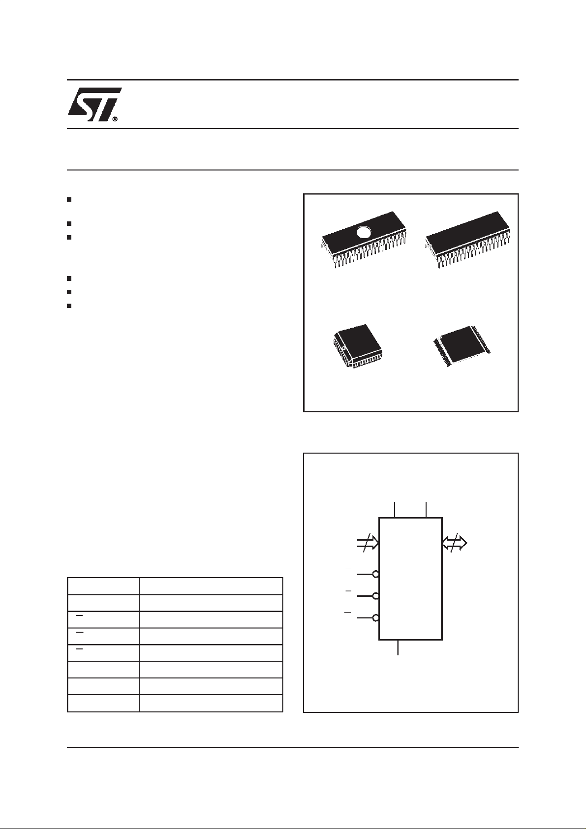
DESCRIPTION
The M27C1024 is a 1 MbitEPROM offered in the
two ranges UV (ultra violet erase) and OTP (one
time programmable). It is ideally suited for microprocessorsystemsrequiringlargedata or program
storage and is organized as 65,536 words of 16
bits.
The FDIP40W(window ceramic frit-seal package)
has a transparent lid which allows the user to
expose the chip to ultraviolet light to erase the bit
pattern. A new pattern can then be written to the
deviceby followingthe programming procedure.
For application where the content is programmed
only one time and erasure is not required, the
M27C1024 is offered in PDIP40, PLCC44 and
TSOP40(10 x 14mm) packages.
40
1
FDIP40W (F)
PLCC44 (C) TSOP40 (N)
Figure1. Logic Diagram
V
CC
16
A0-A15
M27C1024
40
1
PDIP40 (B)
10 x 14mm
V
PP
16
Q0-Q15
Table1. Signal Names
A0-A15 Address Inputs
Q0-Q15 Data Outputs
E Chip Enable
G Output Enable
P Program
V
PP
V
CC
V
SS
September 1998 1/15
Program Supply
Supply Voltage
Ground
P
E
G
M27C1024
V
SS
AI00702B
Page 2
M27C1024
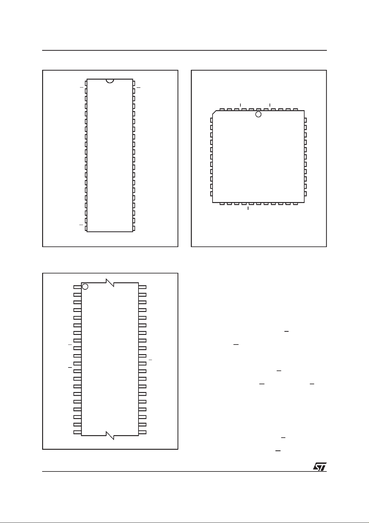
Figure2A. DIP Pin Connections
V
PP
Q15
Q14
Q13
Q12
Q11
Q10
Q9
Q8
V
SS
Q7
Q6
Q5
Q4
Q3
Q2
Q0
1
2
3
4
5
6
7
8
9
10
M27C1024
11
12
13
14
15
16
17
18
19
40
39
38
37
36
35
34
33
32
31
30
29
28
27
26
25
24
23
22
2120
AI00703
V
CC
PE
NC
A15
A14
A13
A12
A11
A10
A9
V
SS
A8
A7
A6
A5
A4
A3
A2Q1
A1
A0G
Figure2B. LCC Pin Connections
Q15
Q13
Q14
Q12
Q11
Q10
Q9 A10
Q8
V
SS
NC
Q6
Q5
Q4
12
Q3
Q2
M27C1024
Q1
Q0
CC
NC
VPPE
V
1
44
23
G
A0
NC
P
A1
NC
A2
A15
A3
A14
34
A4
A13
A12
A11
A9
V
SS
NC
A8Q7
A7
A6
A5
AI00704
Warning: NC = Not Connected.
Figure2C. TSOPPin Connections
A9
1
A10
A11
A12 A6
A13 A5
A14
A15
NC
P
V
CC
V
DQ15
DQ14
DQ13
DQ12 DQ4
DQ11 DQ5
DQ10
DQ9
DQ8
Warning: NC = Not Connected.
10
11
PP
E
20 21
M27C1024
(Normal)
40
31
30
AI01582
V
SS
A8
A7
A4
A3
A2
A1
A0
G
DQ0
DQ1
DQ2
DQ3
DQ6
DQ7
V
SS
Warning: NC = Not Connected.
DEVICEOPERATION
The modes of operations of the M27C1024 are
listedin theOperatingModestable.Asingle power
supplyis required in the read mode. All inputsare
TTL levels except for Vpp and 12V on A9 for
ElectronicSignature.
Read Mode
The M27C1024 has two control functions,both of
which must be logically active in order to obtain
data at the outputs. Chip Enable(E) is the power
control and should be used for device selection.
OutputEnable(G) is the outputcontroland should
be used to gate data to the output pins, independent of device selection. Assuming that the
addresses are stable, the address access time
)isequaltothedelayfromEtooutput(t
(t
AVQV
Data is available at the output after a delayof t
ELQV
OE
from the falling edge of G, assuming that E has
been low and the addresses have been stable for
at least t
AVQV-tGLQV
.
StandbyMode
The M27C1024 has a standby mode which reducestheactive current from 35mAto 100µA.
The M27C1024 is placed in the standby mode by
applyinga TTLhigh signal to theE input. When in
thestandbymode, theoutputsare ina highimpedance state,independentof the G input.
).
2/15
Page 3
M27C1024
Table2. AbsoluteMaximum Ratings
(1)
Symbol Parameter Value Unit
T
A
T
BIAS
T
STG
V
IO
V
CC
V
A9
V
PP
Notes: 1. Except for therating ”Operating Temperature Range”, stresses above those listed in the Table ”AbsoluteMaximum Ratings”
2. Minimum DC voltage on Input or Output is –0.5V with possible undershoot to –2.0V for a periodlessthan 20ns. Maximum DC
3. Depends on range.
Ambient Operating Temperature
Temperature Under Bias –50 to125
Storage Temperature –65 to150 °C
(2)
Input or Output Voltages (except A9) –2 to7 V
Supply Voltage –2 to7 V
(2)
A9 Voltage –2 to13.5 V
Program Supply Voltage –2 to14 V
may cause permanentdamage to thedevice. These are stress ratings only and operationof the device at these or any other
conditions above those indicated in the Operating sections of this specification is not implied.Exposure to Absolute Maximum
Rating conditions for extended periods may affect device reliability.Refer also to the STMicroelectronics SURE Program and other
relevant qualitydocuments.
voltage on Output is V
+0.5Vwith possible overshoot toVCC+2V for a periodless than 20ns.
CC
(3)
–40 to125 °C
°
C
Table3. Operating Modes
Mode E G P A9 V
Read V
Output Disable V
Program V
Verify V
Program Inhibit V
Standby V
Electronic Signature V
Note: X= VIHor VIL,VID= 12V ±0.5V
PP
IL
IL
IL
IL
IH
IH
IL
V
IL
V
IH
XV
V
IL
XXXVPPHi-Z
XXXV
V
IL
V
IH
XXV
Pulse X V
IL
V
IH
V
IH
XV
CC
CC
or V
or V
PP
SS
SS
XVPPData Output
or V
CC
SS
V
ID
V
CC
Q0 - Q15
Data Output
Hi-Z
Data Input
Hi-Z
Codes
Table4. ElectronicSignature
Identifier A0 Q7 Q6 Q5 Q4 Q3 Q2 Q1 Q0 Hex Data
Manufacturer’s Code V
Device Code V
Note: Outputs Q8-Q15 are set to ’0’.
IL
IH
00100000 20h
100011008Ch
3/15
Page 4
M27C1024
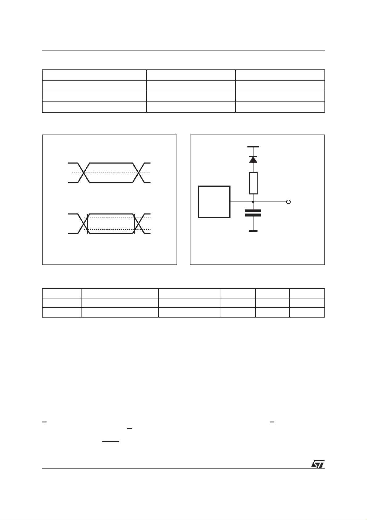
Table5. AC Measurement Conditions
High Speed Standard
Input Rise and Fall Times
Input Pulse Voltages 0 to 3V 0.4V to 2.4V
Input and Output Timing Ref. Voltages 1.5V 0.8V and 2V
≤
10ns
≤
20ns
Figure3. AC TestingInput Output Waveform
High Speed
3V
1.5V
0V
Standard
2.4V
0.4V
Table6. Capacitance
Symbol Parameter Test Condition Min Max Unit
C
IN
C
OUT
Note: 1. Sampled only, not 100% tested.
Input Capacitance VIN=0V 6 pF
Output Capacitance V
(1)
(TA=25°C, f = 1 MHz)
2.0V
0.8V
AI01822
Figure4. AC TestingLoad Circuit
1.3V
1N914
3.3kΩ
DEVICE
UNDER
TEST
C
L
CL= 30pF for High Speed
CL= 100pF for Standard
CLincludes JIGcapacitance
=0V 12 pF
OUT
OUT
AI01823B
Two Line Output Control
BecauseEPROMs areusuallyusedinlargermemory arrays, this product features a 2 line control
functionwhich accommodates the use of multiple
memory connection. The two line control function
allows:
a. the lowest possiblememory powerdissipation,
b. complete assurancethat output bus contention
will not occur.
Forthemostefficientuseofthesetwocontrollines,
E should be decoded and used as the primary
deviceselectingfunction,whileG should be made
a common connection to all devices in the array
and connected to the READline from the system
4/15
controlbus.Thisensuresthat all deselectedmemory devices are in their low power standby mode
and that the output pins are only active when data
is requiredfrom a particular memory device.
SystemConsiderations
The power switching characteristics of Advanced
CMOSEPROMs require careful decoupling of the
devices. The supply current, I
, has three seg-
CC
mentsthat are of interestto the system designer :
the standby current level, the active current level,
and transient current peaks that are producedby
thefalling and rising edges ofE. Themagnitudeof
transientcurrentpeaksisdependentonthecapacitive and inductive loading of the device at the
output.
Page 5
M27C1024
Table7. Read Mode DC Characteristics
(1)
(TA=0 to 70 °C, –40 to 85 °C; –40 to 105 °C or –40 to 125 °C; VCC=5V±5% or 5V ± 10%; VPP=VCC)
Symbol Parameter Test Condition Min Max Unit
I
LI
I
LO
I
CC
I
CC1
I
CC2
I
PP
V
IL
V
IH
V
OL
V
OH
Notes: 1. VCCmust be applied simultaneouslywith or before VPPand removed simultaneously with or afterV
2. Maximum DC voltage on Output is VCC+0.5V.
Input Leakage Current 0V ≤ VIN≤ V
Output Leakage Current 0V≤V
Supply Current
E=V
= 0mA, f = 5MHz
I
OUT
Supply Current (Standby) TTL E= V
≤
OUT
,G=VIL,
IL
IH
CC
V
CC
Supply Current (Standby) CMOS E > VCC–0.2V 100 µA
Program Current VPP=V
CC
Input Low Voltage –0.3 0.8 V
(2)
Input High Voltage 2 VCC+1 V
Output Low Voltage IOL= 2.1mA 0.4 V
Output High VoltageTTL IOH= –400µA 2.4 V
Output High VoltageCMOS I
= –100µAV
OH
CC
– 0.7 V
PP.
±10 µA
10
±
A
µ
35 mA
1mA
100
A
µ
Table8A. ReadModeAC Characteristics
(1)
(TA=0 to 70 °C, –40 to 85 °C; –40 to 105 °C or –40 to 125 °C; VCC=5V±5% or 5V ± 10%; VPP=VCC)
M27C1024
Symbol Alt Parameter Test Condition
-35
(3)
-45
Min Max Min Max Min Max
t
t
AVQV
t
ELQV
t
GLQV
(2)
t
EHQZ
(2)
t
GHQZ
t
AXQX
Notes: 1. VCCmust be applied simultaneouslywith or before VPPand removed simultaneously with or afterV
2. Sampled only, not 100% tested.
3. Speed obtainedwith High Speed AC measurementconditions.
Address Valid to Output Valid E = VIL,G=V
ACC
tCEChip Enable Low to Output Valid G = V
tOEOutput Enable Low to Output Valid E = V
tDFChip Enable High to Output Hi-Z G = V
tDFOutput Enable High to Output Hi-Z E = V
Address Transition to Output
t
OH
Transition
E=V
,G=VIL000ns
IL
IL
IL
IL
IL
IL
35 45 55 ns
35 45 55 ns
20 25 30 ns
030030030ns
030030030ns
(3)
PP.
-55
Unit
(3)
5/15
Page 6

M27C1024
Table8B. ReadModeAC Characteristics
(1)
(TA=0 to 70 °C, –40 to 85 °C; –40 to 105 °C or –40 to 125 °C; VCC=5V±5% or 5V ± 10%; VPP=VCC)
M27C1024
Symbol Alt Parameter Test Condition
-70 -80/-90
-10/-12/
-15/-20
Unit
Min Max Min Max Min Max
t
t
AVQV
t
ELQV
t
GLQV
(2)
t
EHQZ
(2)
t
GHQZ
t
AXQX
Notes: 1. VCCmust be applied simultaneouslywith or before VPPand removed simultaneously with or afterV
2. Sampled only, not 100% tested.
Address Valid to Output Valid E = VIL,G=V
ACC
tCEChip Enable Low to Output Valid G = V
tOEOutput Enable Low to Output Valid E = V
tDFChip Enable High to Output Hi-Z G = V
tDFOutput Enable High to Output Hi-Z E = V
Address Transition to Output
t
OH
Transition
,G=VIL000ns
E=V
IL
IL
IL
IL
IL
IL
70 80 100 ns
70 80 100 ns
35 40 50 ns
0 30 0 30 0 30 ns
0 30 0 30 0 30 ns
PP.
Figure5. Read Mode AC Waveforms
A0-A15
E
G
Q0-Q15
tAVQV
tELQV
VALID
tGLQV
VALID
tAXQX
tEHQZ
tGHQZ
Hi-Z
AI00705B
6/15
Page 7

M27C1024
Table9. ProgrammingMode DC Characteristics
(1)
(TA=25°C; VCC=6.25V ± 0.25V;VPP=12.75V± 0.25V)
Symbol Parameter Test Condition Min Max Unit
I
LI
I
CC
I
PP
V
IL
V
IH
V
OL
V
OH
V
ID
Note: 1. VCCmust be applied simultaneouslywith or before VPPand removed simultaneously with or afterVPP.
Input Leakage Current 0≤V
Supply Current 50 mA
Program Current E = V
Input Low Voltage –0.3 0.8 V
Input High Voltage 2 VCC+ 0.5 V
Output Low Voltage IOL= 2.1mA 0.4 V
Output High VoltageTTL IOH= –400µA 2.4 V
A9 Voltage 11.5 12.5 V
Table10. ProgrammingMode AC Characteristics
(1)
V
≤
IN
IH
IL
10
±
50 mA
(TA=25°C; VCC=6.25V ± 0.25V;VPP=12.75V± 0.25V)
Symbol Alt Parameter TestCondition Min Max Unit
t
AVPL
t
AS
Address Valid to Program Low 2
A
µ
s
µ
t
QVPL
t
VPHPL
t
VCHPL
t
ELPL
t
PLPH
t
PHQX
t
QXGL
t
GLQV
(2)
t
GHQZ
t
GHAX
Notes: 1. VCCmust be applied simultaneouslywith or before VPPand removed simultaneously with or afterVPP.
2. Sampled only, not 100% tested.
t
t
VPS
t
VCS
t
CES
t
PW
t
t
OES
t
t
DFP
t
DS
DH
OE
AH
Input Validto Program Low 2
VPPHigh to Program Low 2
VCCHigh to Program Low 2
Chip Enable Low to Program Low 2
Program Pulse Width 95 105
Program High to Input Transition 2
Input Transition to Output Enable
Low
2
Output Enable Low to Output Valid 100 ns
Output Enable High to Output Hi-Z 0 130 ns
Output Enable High to Address
Transition
0ns
s
µ
s
µ
s
µ
s
µ
s
µ
s
µ
s
µ
7/15
Page 8

M27C1024
Figure6. Programmingand VerifyModes AC Waveforms
A0-A15
Q0-Q15
V
PP
V
CC
E
P
G
VALID
tAVPL
DATA IN DATA OUT
tQVPL
tVPHPL
tVCHPL
tELPL
tPLPH
PROGRAM VERIFY
tPHQX
tQXGL
tGLQV
tGHQZ
tGHAX
AI00706
DEVICEOPERATION
(cont’d)
The associated transient voltage peaks can be
suppressed by complying with thetwo line output
control and by properly selected decoupling capacitors. It is recommended that a 0.1µF ceramic
capacitor be used on every device between V
CC
andVSS. Thisshouldbea highfrequencycapacitor
of low inherent inductance and should be placed
as close to the device as possible. In addition, a
4.7µF bulk electrolytic capacitor should be used
betweenVcc and V
for everyeight devices. The
SS
bulk capacitor should be located near the power
supply connectionpoint. The purpose of the bulk
capacitoris to overcome the voltage drop caused
by the inductive effects of PCB traces.
Programming
Whendelivered(and aftereach ’1’serasureforUV
EPROM), all bits of the M27C1024 are in the ’1’
state. Data is introduced by selectively programming ’0’s into the desired bit locations. Although
only’0’s willbe programmed,both’1’s and’0’s can
8/15
be present in the data word. The only way to
changea ’0’to a ’1’is by die exposureto ultraviolet
light (UV EPROM). The M27C1024 is in the programmingmode when V
at V
and P is pulsed to VIL. The data to be
IL
inputis at 12.75V,E is
PP
programmedis applied to 16 bits in parallel to the
data output pins. The levels required for the addressand data inputs are TTL. V
be 6.25V ±
0.25V.
is specifiedto
CC
PRESTOII ProgrammingAlgorithm
PRESTO II Programming Algorithm allows programming of the whole array with a guaranteed
margin,in a typical time of 6.5 seconds.Programming with PRESTO II consists of applying a sequenceof100µsprogrampulsestoeachworduntil
a correct verify occurs (see Figure 7). During programmingand verify operation,a MARGINMODE
circuitisautomaticallyactivatedin orderto guarantee that each cell is programmed with enough
margin. Nooverprogrampulseisappliedsincethe
verifyin MARGIN MODEprovidesnecessarymargin to each programmedcell.
Page 9

M27C1024
Figure7. ProgrammingFlowchart
VCC= 6.25V, VPP= 12.75V
n=0
P = 100µs Pulse
NO
NO
VERIFY
YES
Last
NO
Addr
YES
CHECK ALL WORDS
1st: VCC=6V
2nd: VCC= 4.2V
++ Addr
AI00707C
YES
++n
=25
FAIL
ProgramInhibit
Programming of multiple M27C1024s in parallel
with different data is also easily accomplished.
Except for E, all like inputs including G of the
parallel M27C1024 may be common. A TTL low
level pulse applied to a M27C1024’sP input, with
E low and V
at 12.75V, will program that
PP
M27C1024. A high level E input inhibits theother
M27C1024sfrom being programmed.
ProgramVerify
A verify (read) should be performed on the programmedbitsto determinethattheywerecorrectly
programmed. The verify is accomplished with E
and G at V
, P at VIH,VPPat 12.75Vand VCCat
IL
6.25V.
On-BoardProgramming
TheM27C1024canbe directlyprogrammedin the
application circuit. See the relevant Application
NoteAN620.
ElectronicSignature
The Electronic Signature (ES) mode allows the
readingout of a binarycode from an EPROMthat
will identify its manufacturerand type. This mode
is intendedfor use by programmingequipment to
automaticallymatch the deviceto be programmed
withitscorrespondingprogrammingalgorithm.The
ES mode is functional in the 25°C± 5°Cambient
temperaturerange that is required whenprogrammingthe M27C1024.ToactivatetheESmode, the
programmingequipmentmustforce11.5Vto12.5V
on address line A9 of the M27C1024 with V
V
= 5V. Two identifier bytes may then be se-
CC
PP
quenced from the device outputs by toggling addresslineA0from V
must be held at V
mode. Byte 0 (A0=V
turercodeandbyte 1(A0=V
toVIH. Allotheraddresslines
IL
during Electronic Signature
IL
) represents the manufac-
IL
) thedeviceidentifier
IH
code. For the STMicroelectronics M27C1024,
thesetwo iden-tifier bytesare given in Table4 and
canbe read-out on outputsQ0 to Q7.
ERASUREOPERATION(appliesto UV EPROM)
The erasure characteristics of the M27C1024 is
such that erasure begins when the cells are exposed to light with wavelengths shorter than approximately4000 Å.It shouldbenotedthatsunlight
and some type of fluorescent lamps have wavelengthsinthe3000-4000Årange.Researchshows
that constant exposure to room level fluorescent
lightingcoulderase a typicalM27C1024 in about3
years,while it would take approximately1 weekto
cause erasure when exposed to direct sunlight. If
the M27C1024 is tobe exposed to thesetypes of
lighting conditions for extended periods of time, it
is suggested that opaque labels be put over the
M27C1024 window to prevent unintentional erasure.Therecommendederasureprocedureforthe
M27C1024 is exposure to short wave ultraviolet
lightwhich haswavelength2537Å. Theintegrated
dose(i.e. UVintensityxexposuretime)forerasure
should be a minimum of 15 W-sec/cm
2
. The erasure time with this dosage is approximately15 to
20 minutes using an ultraviolet lamp with
12000 µW/cm
2
power rating. The M27C1024
shouldbe placedwithin 2.5 cm (1inch) of thelamp
tubesduringthe erasure.Somelamps havea filter
on their tubes which should be removed before
erasure.
=
9/15
Page 10

M27C1024
ORDERING INFORMATION SCHEME
Example: M27C1024 -12 X C 1 X
Speed
(1)
-35
-45
-55
(1)
(1)
35ns
45ns
55ns
-70 70ns
-80 80ns
V
blank
X
Tolerance
CC
±
±
10%
5%
Package
F FDIP40W
B PDIP40
C PLCC44
N TSOP40
10 x 14mm
Temperature Range
1 0 to 70°C
6 –40 to 85°C
7 –40 to 105°C
3 –40 to 125°C
Option
X Additional
Burn-in
TR Tape& Reel
Packing
-90 90ns
-10 100ns
-12 120ns
-15 150ns
-20 200ns
-10 100ns
Note: 1. High Speed, see AC Characteristics section for furtherinformation.
Fora listof availableoptions(Speed,Package,etc...)orforfurtherinformationonanyaspectof thisdevice,
pleasecontact the STMicroelectronicsSales Officenearest to you.
10/15
Page 11

FDIP40W - 40 pin Ceramic Frit-sealDIP,with window
M27C1024
Symb
A 5.72 0.225
A1 0.51 1.40 0.020 0.055
A2 3.91 4.57 0.154 0.180
A3 3.89 4.50 0.153 0.177
B 0.41 0.56 0.016 0.022
B1 1.45 – – 0.057 – –
C 0.23 0.30 0.009 0.012
D 51.79 52.60 2.039 2.071
D2 48.26 – – 1.900 – –
E 15.24 – – 0.600 – –
E1 13.06 13.36 0.514 0.526
e 2.54 – – 0.100 – –
eA 14.99 – – 1.900 – –
eB 16.18 18.03 0.637 0.710
L 3.18 0.125
S 1.52 2.49 0.060 0.098
∅ 8.13 – – 0.320 – –
α 4° 11° 4° 11°
N40 40
Typ Min Max Typ Min Max
mm inches
Drawing isnot to scale.
A2
B1 B e
D2
D
S
N
1
A3A1A
L
α
C
eA
eB
∅
E1 E
FDIPW-a
11/15
Page 12

M27C1024
PDIP40 - 40 pin Plastic DIP,600 mils width
Symb
Typ Min Max Typ Min Max
A 4.45 – – 0.175 – –
A1 0.64 0.38 – 0.025 0.015 –
A2 3.56 3.91 0.140 0.154
B 0.38 0.53 0.015 0.021
B1 1.14 1.78 0.045 0.070
C 0.20 0.31 0.008 0.012
D 51.78 52.58 2.039 2.070
D2 48.26 – – 1.900 – –
E 14.80 16.26 0.583 0.640
E1 13.46 13.99 0.530 0.551
e1 2.54 – – 0.100 – –
eA 15.24 – – 0.600 –
eB 15.24 17.78 0.600 0.700
L 3.05 3.81 0.120 0.150
S 1.52 2.29 0.060 0.090
α
N40 40
mm inches
0
°
15
°
0É 15
°
Drawing isnot to scale.
12/15
B1 B e1
D2
D
S
N
1
A2A1A
E1 E
L
α
C
eA
eB
PDIP
Page 13

PLCC44 - 44 lead Plastic Leaded Chip Carrier,square
M27C1024
Symb
Typ Min Max Typ Min Max
A 4.20 4.70 0.165 0.185
A1 2.29 3.04 0.090 0.120
B 0.33 0.53 0.013 0.021
B1 0.66 0.81 0.026 0.032
D 17.40 17.65 0.685 0.695
D1 16.51 16.66 0.650 0.656
D2 14.99 16.00 0.590 0.630
E 17.40 17.65 0.685 0.695
E1 16.51 16.66 0.650 0.656
E2 14.99 16.00 0.590 0.630
e 1.27 – – 0.050 – –
j 0.89 – – 0.035 – –
N44 44
CP 0.10 0.004
mm inches
D
D1
1N
Ne E1 E
Nd
PLCC
Drawing isnot to scale.
R
F
0.51 (.020)
1.14 (.045)
D2/E2
A1
A2
B1
e
B
A
CP
13/15
Page 14

M27C1024
TSOP40- 40 lead Plastic Thin Small Outline, 10 x 14mm
Symb
Typ Min Max Typ Min Max
A 1.20 0.047
A1 0.05 0.15 0.002 0.006
A2 0.95 1.05 0.037 0.041
B 0.17 0.27 0.007 0.011
C 0.10 0.21 0.004 0.008
D 13.80 14.20 0.543 0.559
D1 12.30 12.50 0.484 0.492
E 9.90 10.10 0.390 0.398
e 0.50 – – 0.020 – –
L 0.50 0.70 0.020 0.028
α
N40 40
CP 0.10 0.004
mm inches
0
°
5
°
0
°
5
°
Drawing isnot to scale.
1N
E
N/2
D1
D
DIE
TSOP-a
A2
e
B
A
CP
C
LA1 α
14/15
Page 15

M27C1024
Information furnished is believed to be accurate and reliable. However, STMicroelectronics assumes no responsibility forthe consequences
ofuse of such informationnorfor anyinfringement of patents or other rights of third parties which may resultfrom itsuse. Nolicense is granted
by implicationor otherwise under any patent or patent rights of STMicroelectronics. Specificationsmentionedin this publication are subject to
change without notice. This publication supersedes and replaces all information previously supplied. STMicroelectronics products are not
authorized for use as critical components in lifesupport devices or systems without express written approval of STMicroelectronics.
The ST logoisa registered trademark of STMicroelectronics
1998 STMicroelectronics - All Rights Reserved
Australia - Brazil - Canada - China - France - Germany - Italy - Japan - Korea - Malaysia- Malta - Mexico - Morocco - TheNetherlands -
Singapore - Spain - Sweden - Switzerland - Taiwan - Thailand - United Kingdom - U.S.A.
STMicroelectronics GROUP OF COMPANIES
15/15
 Loading...