

Datasheet M27512-F6, M27512-F1, M27512-3F6, M27512-3F1, M27512-2F1 Datasheet (SGS Thomson Microelectronics)
...Page 1
1/11
NOT FOR NEW DESIGN
November 2000
This is information on a product still in production but not recommended for new designs.
M27512
NMOS 512 K bit (6 4Kb x 8) UV EPROM
■ FAST ACCESS TIME: 200ns
■ EXTENDED TEMPERATURE RANGE
■ SINGLE 5V SUPPLY VOLTAGE
■ LOW STANDBY CURRENT: 40mA max
■ TTL COMPATIBLE DURING READ and
PROGRAM
■ FAST PROGRAMMING ALGORITHM
■ ELECTRONIC SIGNATURE
■ PROGRAMMING VOLTAGE: 12V
DESCRIPTION
The M27512 is a 524,288 bit UV erasable and
electrically programmable memory EPRO M. It is
organized as 65,536 words by 8 bits.
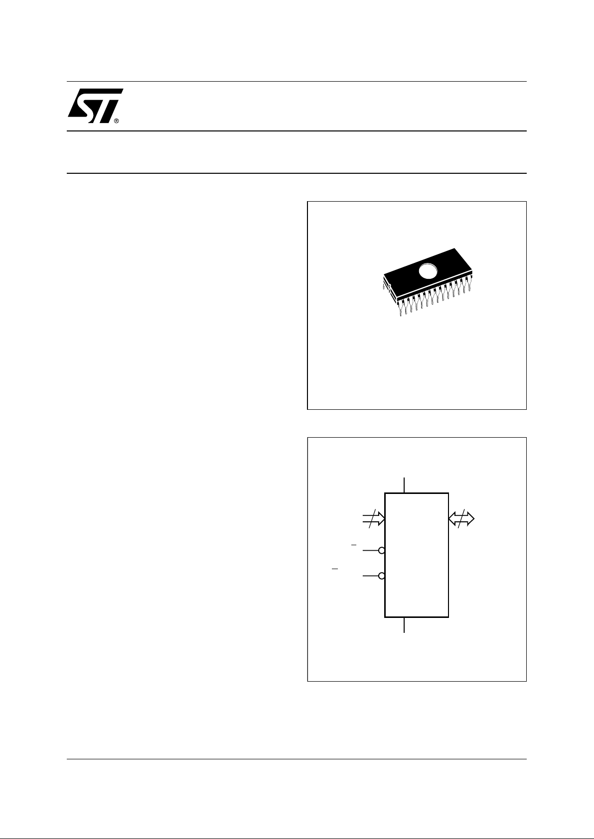
The M27512 is housed in a 28 Pin Window Ceramic Frit-Seal Dual-in-Line package. The transparent lid allows the user to expose the chip to
ultraviolet light to erase the bit pattern. A new pattern can then be written to the device by following
the programming procedure.
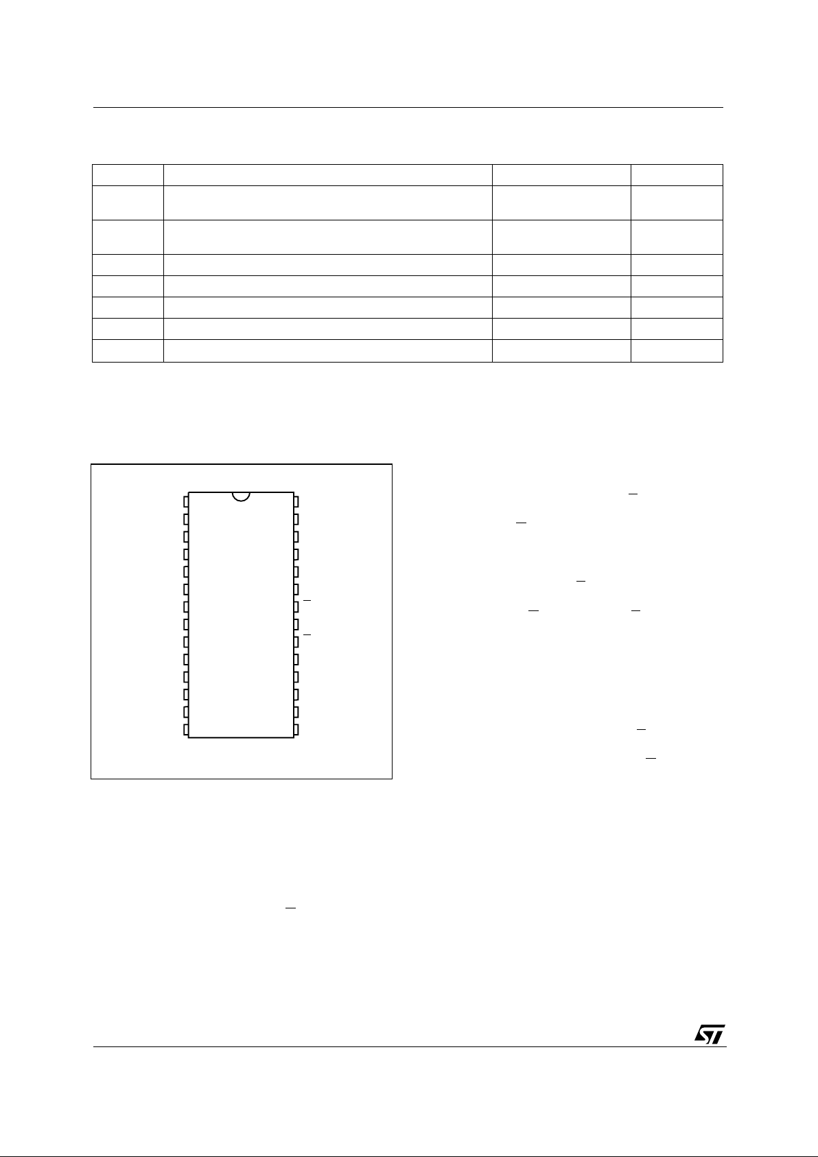
Figure 1. Logic Diagram
AI00765B
16
Q0-Q7
V
CC
M27512
GV
PP
V
SS
8
A0-A15
E
1
28
FDIP28W (F)
Page 2
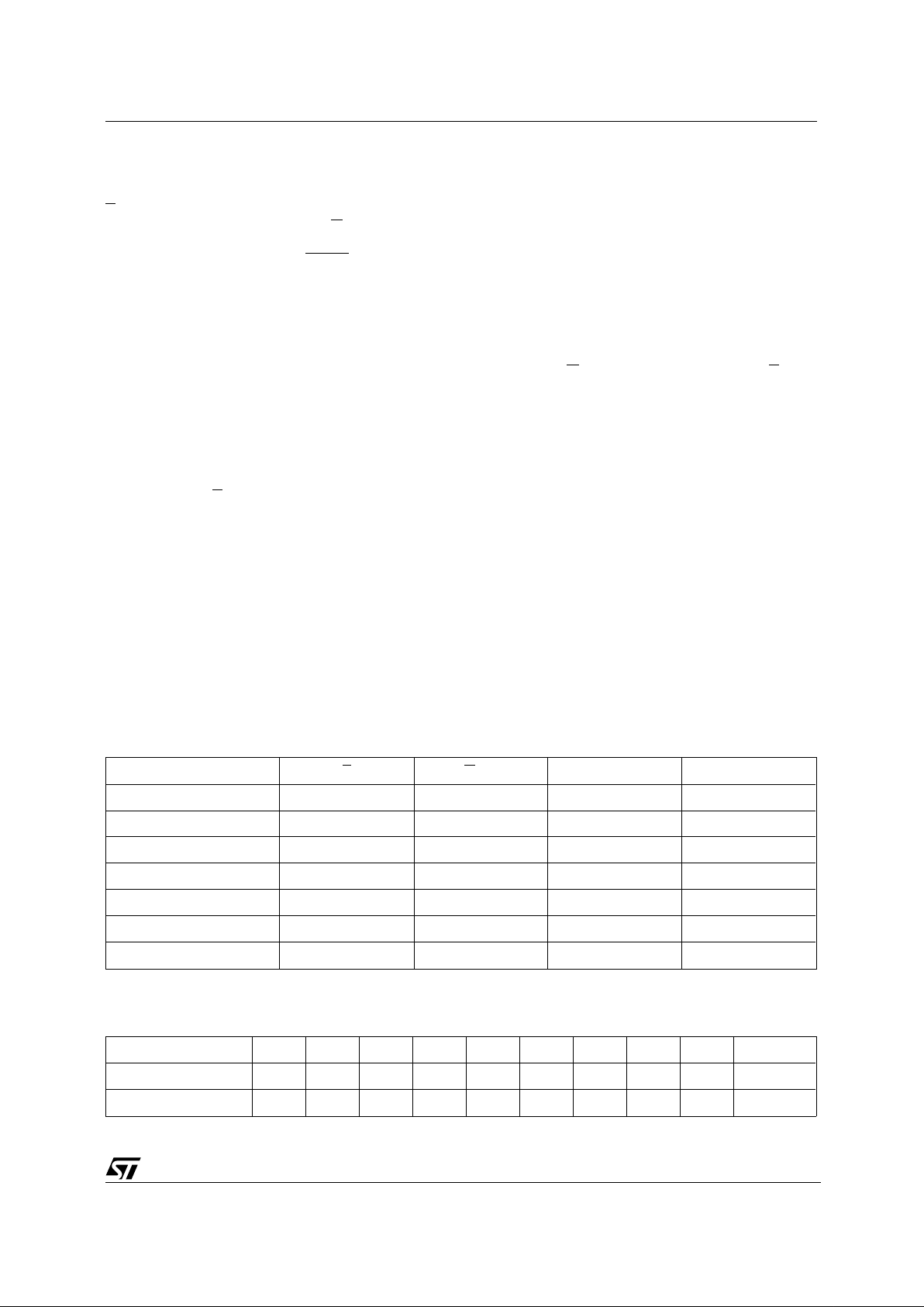
A1
A0
Q0
A7
A4
A3
A2
A6
A5
A13
A10
A8
A9
Q7
A14
A11
GV
PP
E
Q5Q1
Q2
Q3V
SS
Q4
Q6
A12
A15 V
CC
AI00766
M27512
8
1
2
3
4
5
6
7
9
10
11
12
13
14
16
15
28
27
26
25
24
23
22
21
20
19
18
17
Figure 2. DIP Pin Co n nect ion s
Symbol Parameter Value Unit
T
A
Ambient Operating T empera ture
Grade 1
Grade 6
0 to 70
–40 to 85
°C
T
BIAS
Temperature Under Bias
Grade 1
Grade 6
–10 to 80
–50 to 95
°C
T
STG
Storage Temperature –65 to 125 °C
V
IO
Input or Output Voltages –0.6 to 6.5 V
V
CC
Supply Voltage –0.6 to 6.5 V
V
A9
A9 Voltage –0.6 to 13.5 V
V
PP
Program Supply –0.6 to 14 V
Note: Except for the rating "Operating Temperature Range", st resses above t hose listed in t he Ta ble "Absolute Max imum R atings" may c ause
permanent damage to the device. These are stress ratings only and operation of the device at these or any other conditions above those
indicated in the Operating sections of this specification is not implied. Exposure to Absolute Maximum Ratin g conditions for extended periods
may affect device reliability. Refer also to the STMicroelectronics SURE Program and other relevant quality document.
Table 2. Absol ute Maxim u m Ratin g s
DEVICE OPERATION
The six modes of operations of the M27512 are
listed in the Operating Modes table. A single 5V
power supply is required in the read mode. All
inputs are TTL levels except for
GVPP and 12V on
A9 for Electronic Signature.
Read Mode
The M27512 has two control functions, both of
which must be logically active in order to obtain
data at the outputs. Chip Enable (
E) is the power
control and should be used for device selection.
Output Enable (
G) is the output control and should
be used to gate data to the output pins, independent of device selection. Assuming that the
addresses are s table, address access time (t
AVQV
)
is equal to the delay from
E to output (t
ELQV
). Data
is available at the out puts after d elay of t
GLQV
from
the falling edge of
G, assuming that E has been low
and the addresses have been stable for at least
t
AVQ V-tGLQV
.
Stand by Mod e
The M27512 has a standby mode which reduces
the maximum active power current f rom 125m A to
40mA. The M27512 is placed in the standby mod e
by applying a TTL high signal to the
E input. Wh en
in the standby mode, the outputs are in a high
impedance state, independent of the
GVPP input.
Two Line Output Control
Because EPROM s are usually used in larger memory arrays, the product features a 2 line control
function which accommodates the use of multiple
memory connection. The two line control function
allows :
a. the lowest possible memory power dissipation,
b. complete assurance that output bus c ontent io n
will not occur.
M27512
2/11
Page 3
For the most efficient us e of these two control lines,
E should be decoded and used as the primary
device selecting function, while
GVPP should be
made a common connection to all devices in the
array and connected to the
READ line from the
system control bus. This ensures that all deselected memory devices are in their low power
standby mode and that the output pins are only
active when data is r equired from a particular memory device.
System Considerati on s
The power switching characteristics of fast
EPROMs require careful decoupling of the devices.
The supply current, I
CC
, has three segments that
are of interes t to the s ystem designer : the s tandby
current level, the active c urrent level, and t ransient
current peaks that are produced by the falling and
rising edges of
E. The magnitude of the transient
current peaks is dependent on the capacitive and
inductive loading of the device at the output. The
associated transient voltage peaks can be suppressed by complying with the two line output
control and by properly selected decoupling capacitors. It is recommenced that a 1µF ceramic
capacitor be used on every device between V
CC
and VSS. This should be a high frequency capacitor
of low inherent inductance and should be placed
as close to the device as possible. In addition, a
4.7µF bulk electrolytic capacitor should be used
between V
CC
and VSS for every eight devices. Th e
bulk capacitor should be located near the power
supply connection point. The purpose of the bulk
capacitor is to overcome the voltage drop caused
by the inductive effects of PC B trac es.
Programming
When delivered, and after each erasure, all bits of
the M27512 are in the “1" stat e. Data is intr oduce d
by selectively programming ”0s" into the desired bit
locations. Although only “0s” will be programmed,
both “1s” and “0s” can be present in the dat a word.
The only way to change a “0" to a ”1" is by ultraviolet
light erasure. The M27512 is in the programming
mode when
GVPP input is at 12.5V and E is at
TTL-low. The data to be programmed is applied 8
bits in parallel to the data output pins. The levels
required for the address and data inputs are TTL.
The M27512 can us e PRESTO P rogramming Algorithm that drastically reduces the programming
time (typically less than 50 seconds). Never theless
to achieve compatibility with all programming
equipment, the standard Fast Programming Algorithm may also be used.
Fast Prog rammi ng Alg or ithm
Fast Programming Algorithm rapidly programs
M27512 EPROMs using an efficient and reliable
method suited to the production programming environment. Programming reliability is also ens ured
as the incremental program margin of each byte is
continually monitored to determine when it has
been successfully program med. A flowc hart of the
M27512 Fast Programming Algorithm is shown in
Figure 8.
Mode E GV
PP
A9 Q0 - Q7
Read V
IL
V
IL
X Data Out
Output Disable V
IL
V
IH
X Hi-Z
Program V
IL
Pulse V
PP
X Data In
Verify V
IH
V
IL
X Data Out
Program Inhibit V
IH
V
PP
X Hi-Z
Standby V
IH
X X Hi-Z
Electronic Signature V
IL
V
IL
V
ID
Codes
Note: X = VIH or VIL, VID = 12V ± 0.5%.
Table 3. Operating Modes
Identifier A0 Q7 Q6 Q5 Q4 Q3 Q2 Q1 Q0 Hex Data
Manufacturer’s Code V
IL
00100000 20h
Device Code V
IH
00001101 0Dh
T a b le 4. Electro ni c Sig n atu r e
DEVICE OPERATION (cont’d)
M27512
3/11
Page 4
AI00827
2.4V
0.45V
2.0V
0.8V
Figure 3. AC T est ing Input Ou tput Waveform s
Input Rise and Fall Times ≤ 20ns
Input Pulse Voltages 0.45V to 2.4V
Input and Output Timing Ref. Voltages 0.8V to 2.0V
AC MEASUREMENT CONDITIONS
AI00828
1.3V
OUT
CL = 100pF
CL includes JIG capacitance
3.3kΩ
1N914
DEVICE
UNDER
TEST
Figure 4. AC Testing L oad Circui t
Note that Output Hi-Z is defined as the point where data
is no longer driven.
Symbol Parameter Test Condition Min Max Unit
C
IN
Input Capacitance VIN = 0V 6 pF
C
OUT
Output Capacitance V
OUT
= 0V 12 pF
Note: 1. Sampled only, not 100% tested.
T able 5. Capacitance
(1)
(TA = 25 °C, f = 1 MHz )
AI00735
tAXQX
tEHQZ
DATA OUT
A0-A15
E
G
Q0-Q7
tAVQV
tGHQZ
tGLQV
tELQV
VALID
Hi-Z
Figure 5. Read Mode AC Wav efo rm s
M27512
4/11
Page 5

Symbol Alt Parameter
Test
Condition
M27512
Unit
-2, -20 blank, -2 5 -3
Min Max Min Max Min Max
t
AVQV
t
ACC
Address Valid to Output Valid
E = VIL,
G = V
IL
200 250 300 ns
t
ELQV
t
CE
Chip Enable Low to Output Valid G = V
IL
200 250 300 ns
t
GLQV
t
OE
Output Enable Low to Output Valid E = V
IL
75 100 120 ns
t
EHQZ
(2)
t
DF
Chip Enable High to Output Hi-Z G = V
IL
0 55 0 60 0 105 ns
t
GHQZ
(2)
t
DF
Output Enable High to Output Hi-Z E = V
IL
0 55 0 60 0 105 ns
t
AXQX
t
OH
Address Transition to Output
Transition
E = VIL,
G = V
IL
000 ns
Notes: 1. VCC must be applied simult aneously with or before VPP and removed simultaneously or after VPP.
2. Sampled only, not 100% tested.
T ab le 7. Read Mod e AC Charact eristi cs
(1)
(TA = 0 to 70 °C or –40 to 85 °C; VCC = 5V ± 5% or 5V ± 10%; VPP = VCC)
Symbol Parameter Test Condition Min Max Unit
I
LI
Input Leakage Current 0 ≤ VIN ≤ V
CC
±10 µA
I
LO
Output Leakage Current V
OUT
= V
CC
±10 µA
I
CC
Supply Current E = VIL, G = VIL 125 mA
I
CC1
Supply Current (Standby) E = V
IH
40 mA
V
IL
Input Low Voltage –0.1 0.8 V
V
IH
Input High Voltage 2 VCC + 1 V
V
OL
Output Low Voltage IOL = 2.1mA 0.45 V
V
OH
Output High Voltage IOH = –400µA 2.4 V
Note: 1. VCC must be applied simult aneously with or before VPP and removed simultaneously or after VPP.
T ab le 6. Read Mode DC Characteristi cs
(1)
(TA = 0 to 70 °C or –40 to 85 °C; VCC = 5V ± 5% or 5V ± 10%; VPP = VCC)
Symbol Parameter Test Condition Min Max Unit
I
LI
Input Leakage Current VIL ≤ VIN ≤ V
IH
±10 µA
I
CC
Supply Current 150 mA
I
PP
Program Current E = V
IL
50 mA
V
IL
Input Low Voltage –0.1 0.8 V
V
IH
Input High Voltage 2 VCC + 1 V
V
OL
Output Low Voltage IOL = 2.1mA 0.45 V
V
OH
Output High Voltage IOH = –400µA 2.4 V
V
ID
A9 Voltage 11.5 12.5 V
Note: 1. VCC must be applied simult aneously with or before VPP and removed simultaneously or after VPP.
T ab le 8. Program ming Mode DC Char acterist ics
(1)
(TA = 25 °C; VCC = 6.25V ± 0.25V; VPP = 12.75V ± 0.25V )
M27512
5/11
Page 6

Symbol Alt Parameter Test Condition Min Max Unit
t
AVEL
t
AS
Address Valid to Chip Enable
Low
2 µs
t
QVEL
t
DS
Input Valid to Chip Enable Low 2 µs
t
VCHEL
t
VCS
VCC High to Chip Enable Low 2 µs
t
VPHEL
t
OES
VPP High to Chip Enable Low 2 µs
t
VPLVPH
t
PRT
VPP Rise Time 50 ns
t
ELEH
t
PW
Chip Enable Program Pulse
Width (Initial)
Note 2 0.95 1.05 ms
t
ELEH
t
OPW
Chip Enable Program Pulse
Width (Overprogram)
Note 3 2.85 78.75 ms
t
EHQX
t
DH
Chip Enable High to Input
Transition
2 µs
t
EHVPX
t
OEH
Chip Enable High to V
PP
Transition
2 µs
t
VPLEL
t
VR
VPP Low to Chip Enable Low 2 µs
t
ELQV
t
DV
Chip Enable Low to Output
Valid
1 µs
t
EHQZ
(4)
t
DF
Chip Enable High to Output HiZ
0 130 ns
t
EHAX
t
AH
Chip Enable High to Address
Transition
0ns
Notes. 1. VCC must be applied simultaneously with or before VPP and removed simultaneously or after VPP.
2. The Initial Program Pulse width tolerance is 1 ms ± 5%.
3. The length of the Over-program Pulse varies from 2.85 ms to 78.95 ms, depending on the multiplication value of the iteration counter.
4. Sampled only , n ot 100% tested.
T ab le 10. Program min g Mo de AC C haract eristi cs
(1)
(TA = 25 °C; VCC = 6.25V ± 0.25V; VPP = 12.75V ± 0.25V )
Symbol Alt Parameter Test Condition Min Max Unit
t
A9HVPH
t
AS9
VA9 High to VPP High 2 µs
t
VPHEL
t
VPS
VPP High to Chip Enable Low 2 µs
t
A10HEH
t
AS10
VA10 High to Chip Enable
High (Set)
1 µs
t
A10LEH
t
AS10
VA10 Low to Chip Enable High
(Reset)
1 µs
t
EXA10X
t
AH10
Chip Enable Transition to
VA10 Transition
1 µs
t
EXVPX
t
VPH
Chip Enable Transition to V
PP
Transition
2 µs
t
VPXA9X
t
AH9
VPP Transition to VA9
Transition
2 µs
Note: 1. VCC must be applied simultaneously with or before VPP and removed simultaneously or after VPP.
Tab le 9. MARGIN MO DE AC Ch aracteri stics
(1)
(TA = 25 °C; VCC = 6.25V ± 0.25V; VPP = 12.75V ± 0.25V )
M27512
6/11
Page 7

AI00736B
tA9HVPH tVPXA9X
A8
E
GV
PP
A10 Set
V
CC
tVPHEL
tA10LEH
tEXVPX
tA10HEH
A9
A10 Reset
tEXA10X
Figure 6. MARGIN MO DE AC W aveform
AI00737
tVPLEL
PROGRAM
DATA IN
A0-A15
E
GV
PP
Q0-Q7
DATA OUT
tAVEL
tQVEL
tVCHEL
tVPHEL
tEHQX
tEHVPX
tELEH
tELQV
tEHAX
tEHQZ
VERIFY
VALID
V
CC
Figure 7. Programmi ng and Verify Modes AC Wavefo rm s
Note: A8 High level = 5V; A9 High level = 12V .
M27512
7/11
Page 8

AI00774B
n = 1
Last
Addr
VERIFY
E = 1ms Pulse
++n
> 25
++ Addr
VCC = 6V, VPP = 12.5V
FAIL
CHECK ALL BYTES
VCC = 5V, VPP = 5V
YES
NO
YES
NO
YES
NO
E = 3ms Pulse by n
Figure 8. Fast Programming Flowchart
AI00773B
n = 0
Last
Addr
VERIFY
E = 500µs Pulse
++n
= 25
++ Addr
VCC = 6.25V, VPP = 12.75V
FAIL
CHECK ALL BYTES
VCC = 5V, VPP = 5V
YES
NO
YES
NO
YES
NO
SET MARGIN MODE
RESET MARGIN MODE
Figure 9. PRESTO Programming Flowchart
DEVICE OPERATION (cont’d)
The Fast Programming A lgorithm utilizes two dif ferent pulse types : initial and overprogram. The duration of the i nitial
E pulse(s) is 1ms, which will then
be followed by a longer overprogram pulse of length
3ms by n (n is an iteration counter and is equal to
the number of the initial one millisecond pulses
applied to a particular M27512 location), before a
correct verify occurs. Up to 25 one-millisecond
pulses per byte are provided for before the over
program pulse is applied.
The entire sequence of program pulses is performed at V
CC
= 6V and GVPP = 12.5V (byte verifi-
cations at V
CC
= 6V and GVPP = VIL). When the Fast
Programming cycle has been completed, all bytes
should be compared to the original data with
V
CC
= 5V.
PRESTO Programming Algorithm
PRESTO Programming Algorithm allows to program the whole array with a guaranted margin, in
a typical time of less than 50 seconds (to be compared with 283 seconds for the Fast algorithm).
This can be achieved with the STMicroelectronics
M27512 due to several design innovations described in the next paragraph that improves programming efficien cy and brings adequate margin
for reliability. Before starting the programming the
internal MARGIN MODE circuit is set in order to
guarantee that each cell is programmed with
enough margin.
Then a sequence of 500µs program pulses are
applied to each byte until a correct verify occurs.
No overprogram pulses are applied since the verif y
in MARGIN MODE prov ides th e necessary margin
to each programmed cell.
Program Inhibit
Programming of multiple M2751 2s in parallel with
different data is also easily accomplished. Except
for
E, all like inputs (including GVPP) of the parallel
M27512 may be common. A TTL low level pulse
applied to a M27512’s
E input, with GVpp at 12.5V,
will program that M27512. A high level
E input
inhibits the other M27512s from being programmed.
Program Verify
A verify (read) should be performed on the programmed bits to determine that they were cor rectly
programmed. The verify is accomplished with
GV
pp
and E at VIL. Data should be verified tDV after the
falling edge of
E.
M27512
8/11
Page 9

Electronic Signature
The Electronic Signature mode allows the reading
out of a binary code from an EPROM that will
identify its manufacturer and type. This mode is
intended for use by programming equipment to
automatically matc h the devic e to be pr ogramm e d
with its corresponding programming algorithm.
This mode is functional i n the 25 °C ± 5 °C ambient
temperature ran ge that is required w h en programming the M27512. To activate this mode, the programming equipment must f orce 1 1.5V to 12.5V on
address line A9 of the M27512. T wo identifier bytes
may then be sequenced from the device out puts by
toggling address line A0 from V
IL
to VIH. All other
address lines m ust be held at V
IL
during Electronic
Signature mode, except for A14 and A15 which
should be high. Byte 0 (A0 = V
IL
) represents the
manufacturer code and byte 1 (A0 = V
IH
) the device
identifier code.
ERASU RE O PER A T ION (ap plies to UV EPRO M)
The erasure characteristic of the M27512 is such
that erasure begins when the cells are exposed to
light with wavelengths shorter than approximately
4000 Å. It should be noted that sunlight and some
type of fluorescent lamps have wavelengt hs in t he
3000-4000 Å range. Researc h shows that cons tant
exposure to room level fluore scent lighting could
erase a typical M27512 in about 3 years, while it
would take approximately 1 week to cause erasur e
when expose to direct sunlight . If the M27512 is t o
be exposed to these types of lighting conditions for
extended periods of time, it is suggested that
opaque labels be put over the M27512 window to
prevent unintentional erasure. The recommended
erasure procedure for the M27512 is exposure to
short wave ultraviolet light which has wavelength
2537 Å.
The integrated dose (i.e. UV intensity x exposure
time) for erasure should be a minimum of 15
W-sec/cm
2
. The erasure time with this dosage is
approximately 15 to 20 minut es using an ultraviolet
lamp with 12000 µW/cm
2
power rating. The
M27512 should be placed within 2.5 cm (1 inch) of
the lamp tubes during the erasure. Some lamps
have a filter on their tubes which should be removed before erasure.
Speed and VCC Tolerance
-2 200 ns, 5V ±5%
blank 250 ns, 5V ±5%
-3 300 ns, 5V ±5%
-20 200 ns, 5V ±10%
-25 250 ns, 5V ±10%
Package
F FDIP28W
Temperature Range
1 0 to 70 °C
6 –40 to 85 °C
Example: M27512 -2 F 1
ORDERING INFORMATION SCHEME
For a list of available options (S peed, V
CC
T olerance, Package, etc ) refer to the curr ent Memory Shortfor m
catalogue.
For further inform ation on any aspect of this device, please cont act STMicroelectronics Sales Office nearest
to you.
M27512
9/11
Page 10

FDIPW-a
A2
A1AL
B1 B e1
D
S
E1 E
N
1
Cα
eA
e3
∅
Symb
mm inches
Typ Min Max Typ Min Max
A 5.71 0.225
A1 0.50 1.78 0.020 0.070
A2 3.90 5.08 0.154 0.200
B 0.40 0.55 0.016 0.022
B1 1.17 1.42 0.046 0.056
C 0.22 0.31 0.009 0.012
D 38.10 1.500
E 15.40 15.80 0.606 0.622
E1 13.05 13.36 0.514 0.526
e1 2.54 – – 0.100 – –
e3 33.02 – – 1.300 – –
eA 16.17 18.32 0.637 0.721
L 3.18 4.10 0.125 0.161
S 1.52 2.49 0.060 0.098
∅ 7.11 – – 0.280 – –
α 4° 15° 4° 15°
N28 28
Drawing is not to scale
FDIP28W - 28 pin Ceramic Frit-seal DIP, with window
M27512
10/11
Page 11

11/11
M27512
Information furnished is believed to be accurate and reliable. However, STMicroelectronics assumes no responsibility for the consequences
of use of such information nor for any infringement of patents or other rights of third parties which may result from its use. No license is granted
by implic ation or otherwise under any patent or patent rights of STMi croelectr onics. Specifications mentioned in thi s publicati on are subject
to change without notice. This publication supersedes and replaces all information previously supplied. STMicroelectronics products are not
authorized for use as cri tical comp onents in life support dev i ces or systems wi t hout express written ap proval of STMi croelect ro nics.
The ST log o i s registered trademark of STMicroelectronics
All other nam es are the pro perty of their respectiv e owners
2000 STMi croelectr oni cs - All Rig hts Reserv ed
STMicroelectronics GROUP OF COMPANIES
Australi a - B razil - China - Finland - F rance - Germ any - Hong Kon g - India - Italy - Japan - Mala ysia - Malta - Morocco -
Singapor e - Spain - Swede n - S wi tzerland - United Kingdom - U.S.A .
www.st.com
 Loading...